EP3676838B1 - Reaktion auf leistungsverlust - Google Patents
Reaktion auf leistungsverlust Download PDFInfo
- Publication number
- EP3676838B1 EP3676838B1 EP18851275.0A EP18851275A EP3676838B1 EP 3676838 B1 EP3676838 B1 EP 3676838B1 EP 18851275 A EP18851275 A EP 18851275A EP 3676838 B1 EP3676838 B1 EP 3676838B1
- Authority
- EP
- European Patent Office
- Prior art keywords
- memory cell
- voltage
- level
- logic
- control signal
- Prior art date
- Legal status (The legal status is an assumption and is not a legal conclusion. Google has not performed a legal analysis and makes no representation as to the accuracy of the status listed.)
- Active
Links
Images






Classifications
-
- G—PHYSICS
- G11—INFORMATION STORAGE
- G11C—STATIC STORES
- G11C11/00—Digital stores characterised by the use of particular electric or magnetic storage elements; Storage elements therefor
- G11C11/21—Digital stores characterised by the use of particular electric or magnetic storage elements; Storage elements therefor using electric elements
- G11C11/34—Digital stores characterised by the use of particular electric or magnetic storage elements; Storage elements therefor using electric elements using semiconductor devices
- G11C11/40—Digital stores characterised by the use of particular electric or magnetic storage elements; Storage elements therefor using electric elements using semiconductor devices using transistors
- G11C11/41—Digital stores characterised by the use of particular electric or magnetic storage elements; Storage elements therefor using electric elements using semiconductor devices using transistors forming static cells with positive feedback, i.e. cells not needing refreshing or charge regeneration, e.g. bistable multivibrator or Schmitt trigger
- G11C11/413—Auxiliary circuits, e.g. for addressing, decoding, driving, writing, sensing, timing or power reduction
-
- G—PHYSICS
- G11—INFORMATION STORAGE
- G11C—STATIC STORES
- G11C5/00—Details of stores covered by group G11C11/00
- G11C5/005—Circuit means for protection against loss of information of semiconductor storage devices
-
- G—PHYSICS
- G11—INFORMATION STORAGE
- G11C—STATIC STORES
- G11C16/00—Erasable programmable read-only memories
- G11C16/02—Erasable programmable read-only memories electrically programmable
- G11C16/06—Auxiliary circuits, e.g. for writing into memory
- G11C16/34—Determination of programming status, e.g. threshold voltage, overprogramming or underprogramming, retention
- G11C16/3418—Disturbance prevention or evaluation; Refreshing of disturbed memory data
-
- G—PHYSICS
- G11—INFORMATION STORAGE
- G11C—STATIC STORES
- G11C11/00—Digital stores characterised by the use of particular electric or magnetic storage elements; Storage elements therefor
- G11C11/21—Digital stores characterised by the use of particular electric or magnetic storage elements; Storage elements therefor using electric elements
- G11C11/34—Digital stores characterised by the use of particular electric or magnetic storage elements; Storage elements therefor using electric elements using semiconductor devices
- G11C11/40—Digital stores characterised by the use of particular electric or magnetic storage elements; Storage elements therefor using electric elements using semiconductor devices using transistors
- G11C11/41—Digital stores characterised by the use of particular electric or magnetic storage elements; Storage elements therefor using electric elements using semiconductor devices using transistors forming static cells with positive feedback, i.e. cells not needing refreshing or charge regeneration, e.g. bistable multivibrator or Schmitt trigger
- G11C11/412—Digital stores characterised by the use of particular electric or magnetic storage elements; Storage elements therefor using electric elements using semiconductor devices using transistors forming static cells with positive feedback, i.e. cells not needing refreshing or charge regeneration, e.g. bistable multivibrator or Schmitt trigger using field-effect transistors only
- G11C11/4125—Cells incorporating circuit means for protecting against loss of information
-
- G—PHYSICS
- G11—INFORMATION STORAGE
- G11C—STATIC STORES
- G11C14/00—Digital stores characterised by arrangements of cells having volatile and non-volatile storage properties for back-up when the power is down
- G11C14/0054—Digital stores characterised by arrangements of cells having volatile and non-volatile storage properties for back-up when the power is down in which the volatile element is a SRAM cell
- G11C14/0063—Digital stores characterised by arrangements of cells having volatile and non-volatile storage properties for back-up when the power is down in which the volatile element is a SRAM cell and the nonvolatile element is an EEPROM element, e.g. a floating gate or MNOS transistor
-
- G—PHYSICS
- G11—INFORMATION STORAGE
- G11C—STATIC STORES
- G11C16/00—Erasable programmable read-only memories
- G11C16/02—Erasable programmable read-only memories electrically programmable
- G11C16/06—Auxiliary circuits, e.g. for writing into memory
- G11C16/08—Address circuits; Decoders; Word-line control circuits
-
- G—PHYSICS
- G11—INFORMATION STORAGE
- G11C—STATIC STORES
- G11C16/00—Erasable programmable read-only memories
- G11C16/02—Erasable programmable read-only memories electrically programmable
- G11C16/06—Auxiliary circuits, e.g. for writing into memory
- G11C16/10—Programming or data input circuits
-
- G—PHYSICS
- G11—INFORMATION STORAGE
- G11C—STATIC STORES
- G11C16/00—Erasable programmable read-only memories
- G11C16/02—Erasable programmable read-only memories electrically programmable
- G11C16/06—Auxiliary circuits, e.g. for writing into memory
- G11C16/22—Safety or protection circuits preventing unauthorised or accidental access to memory cells
- G11C16/225—Preventing erasure, programming or reading when power supply voltages are outside the required ranges
-
- G—PHYSICS
- G11—INFORMATION STORAGE
- G11C—STATIC STORES
- G11C16/00—Erasable programmable read-only memories
- G11C16/02—Erasable programmable read-only memories electrically programmable
- G11C16/06—Auxiliary circuits, e.g. for writing into memory
- G11C16/30—Power supply circuits
-
- G—PHYSICS
- G11—INFORMATION STORAGE
- G11C—STATIC STORES
- G11C5/00—Details of stores covered by group G11C11/00
- G11C5/14—Power supply arrangements, e.g. power down, chip selection or deselection, layout of wirings or power grids, or multiple supply levels
- G11C5/143—Detection of memory cassette insertion or removal; Continuity checks of supply or ground lines; Detection of supply variations, interruptions or levels ; Switching between alternative supplies
-
- G—PHYSICS
- G11—INFORMATION STORAGE
- G11C—STATIC STORES
- G11C16/00—Erasable programmable read-only memories
- G11C16/02—Erasable programmable read-only memories electrically programmable
- G11C16/04—Erasable programmable read-only memories electrically programmable using variable threshold transistors, e.g. FAMOS
-
- G—PHYSICS
- G11—INFORMATION STORAGE
- G11C—STATIC STORES
- G11C16/00—Erasable programmable read-only memories
- G11C16/02—Erasable programmable read-only memories electrically programmable
- G11C16/04—Erasable programmable read-only memories electrically programmable using variable threshold transistors, e.g. FAMOS
- G11C16/0483—Erasable programmable read-only memories electrically programmable using variable threshold transistors, e.g. FAMOS comprising cells having several storage transistors connected in series
-
- G—PHYSICS
- G11—INFORMATION STORAGE
- G11C—STATIC STORES
- G11C16/00—Erasable programmable read-only memories
- G11C16/02—Erasable programmable read-only memories electrically programmable
- G11C16/06—Auxiliary circuits, e.g. for writing into memory
- G11C16/26—Sensing or reading circuits; Data output circuits
Definitions
- the present disclosure relates generally to memory and, in particular, the present disclosure relates to methods to respond to power loss in an apparatus.
- RAM random-access memory
- ROM read only memory
- DRAM dynamic random access memory
- SDRAM synchronous dynamic random access memory
- flash memory flash memory
- Flash memory has developed into a popular source of non-volatile memory for a wide range of electronic applications. Flash memory typically use a one-transistor memory cell that allows for high memory densities, high reliability, and low power consumption. Changes in threshold voltage (Vt) of the memory cells, through programming (which is often referred to as writing) of charge storage structures (e.g., floating gates or charge traps) or other physical phenomena (e.g., phase change or polarization), determine the data state (e.g., data value) of each memory cell.
- Vt threshold voltage
- flash memory and other non-volatile memory include personal computers, personal digital assistants (PDAs), digital cameras, digital media players, digital recorders, games, appliances, vehicles, wireless devices, mobile telephones, and removable memory modules, and the uses for non-volatile memory continue to expand.
- PDAs personal digital assistants
- flash memory and other non-volatile memory include personal computers, personal digital assistants (PDAs), digital cameras, digital media players, digital recorders, games, appliances, vehicles, wireless devices, mobile telephones, and removable memory modules, and the uses for non-volatile memory continue to expand.
- a NAND flash memory is a common type of flash memory device, so called for the logical form in which the basic memory cell configuration is arranged.
- the array of memory cells for NAND flash memory is arranged such that the control gate of each memory cell of a row of the array is connected together to form an access line, such as a word line.
- Columns of the array include strings (often termed NAND strings) of memory cells connected together in series between a pair of select gates, e.g., a source select transistor and a drain select transistor.
- Each source select transistor may be connected to a source, while each drain select transistor may be connected to a data line, such as column bit line.
- Variations using more than one select gate between a string of memory cells and the source, and/or between the string of memory cells and the data line, are known.
- memory cells may generally be programmed as what are often termed single-level cells (SLC) or multiple-level cells (MLC).
- SLC may use a single memory cell to represent one digit (e.g., bit) of data.
- a Vt of 2.5V might indicate a programmed memory cell (e.g., representing a logical 0) while a Vt of - 0.5V might indicate an erased cell (e.g., representing a logical 1).
- the erased state in SLC might be represented by any threshold voltage less than or equal to 0V, while the programmed data state might be represented by any threshold voltage greater than 0V.
- MLC uses more than two Vt ranges, where each Vt range indicates a different data state.
- a margin e.g., a certain number of volts
- Multiple-level cells can take advantage of the analog nature of traditional non-volatile memory cells by assigning a bit pattern to a specific Vt range.
- MLC typically uses a memory cell to represent one data state of a binary number of data states (e.g., 4, 8, 16, ...)
- a memory cell operated as MLC may be used to represent a non-binary number of data states. For example, where the MLC uses three Vt ranges, two memory cells might be used to collectively represent one of eight data states.
- a first digit e.g., a least significant bit (LSB), often referred to as lower page (LP) data
- LSB least significant bit
- LP lower page
- a second digit e.g., a most significant bit (MSB), often referred to as upper page (UP) data
- MSB most significant bit
- UP upper page
- eight-level MLC may represent a bit pattern of three bits, including a first digit, e.g., a least significant bit (LSB) or lower page (LP) data; a second digit, e.g., upper page (UP) data; and a third digit, e.g., a most significant bit (MSB) or extra page (XP) data.
- LSB least significant bit
- LP lower page
- UP upper page
- MSB most significant bit
- XP extra page
- the LP data and the UP data may be programmed to the memory cells in a first pass, resulting in four threshold voltage ranges, followed by the XP data (and, possibly, reprogramming of the UP data) in a second pass, resulting in eight threshold voltage ranges.
- programming typically utilizes an iterative process of applying a programming pulse to a memory cell and verifying if that memory cell has reached its desired data state in response to that programming pulse, and repeating that iterative process until that memory cell passes the verification. Once a memory cell passes the verification, it may be inhibited from further programming.
- the iterative process can be repeated with changing (e.g., increasing) voltage levels of the programming pulse until each memory cell selected for the programming operation has reached its respective desired data state, or some failure is declared, e.g., reaching a maximum number of allowed programming pulses during the programming operation.
- prior or lower page bit information is typically stored in a latch or other volatile storage device, such as a latch of a sensing device. In some cases, this information may be read from the memory cells prior to beginning the subsequent pass. If a memory device is powered down abruptly during the subsequent programming pass, or otherwise loses power in an uncontrolled manner, e.g., asynchronous power loss, this lower page data may be lost.
- US 2016/019964 describes a memory device that combines a volatile memory cell and a non-volatile memory cell.
- US 2013/294161 describes a static random-access memory (SRAM)-based non-volatile random-access memory cell structure and array for a fast write speed and low write and read voltage.
- SRAM static random-access memory
- semiconductor used herein can refer to, for example, a layer of material, a wafer, or a substrate, and includes any base semiconductor structure.
- semiconductor is to be understood as including silicon-on-sapphire (SOS) technology, silicon-on-insulator (SOI) technology, thin film transistor (TFT) technology, doped and undoped semiconductors, epitaxial layers of a silicon supported by a base semiconductor structure, as well as other semiconductor structures well known to one skilled in the art.
- SOS silicon-on-sapphire
- SOI silicon-on-insulator
- TFT thin film transistor
- doped and undoped semiconductors epitaxial layers of a silicon supported by a base semiconductor structure, as well as other semiconductor structures well known to one skilled in the art.
- previous process steps may have been utilized to form regions/junctions in the base semiconductor structure, and the term semiconductor can include the underlying layers containing such regions/junctions.
- conductive as used herein, as well as its various related forms, e.g., conduct, conductively, conducting, conduction, conductivity, etc., refers to electrically conductive unless otherwise apparent from the context.
- connecting as used herein, as well as its various related forms, e.g., connect, connected, connection, etc., refers to electrically connecting unless otherwise apparent from the context.
- the present disclosure may facilitate preservation of prior (e.g., lower) page data if a power loss event is indicated during programming of a subsequent (e.g., upper) page of data.
- the present disclosure utilizes a differential storage device having associated logic to initiate (e.g., automatically initiate) backup of the prior page data in response to an indication that a power loss has occurred. Due to its differential nature, determining the data state of the differential storage device may be facilitated with only minor changes in threshold voltage. As such, a verify operation may be unnecessary following programming. Furthermore, programming times might be shortened compared to programming of a typical array of memory cells. It may thus be possible to obtain sufficient programming of the differential storage devices without the need for an added hold-up capacitance or other energy storage device as is typically used to recover from a power loss event.
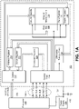
- Figure 1A is a simplified block diagram of a first apparatus, in the form of a memory (e.g., memory device) 100, in communication with a second apparatus, in the form of a processor 130, and a third apparatus, in the form of a power supply 136, as part of a fourth apparatus, in the form of an electronic system.
- the power supply 136 may be external to an electronic system containing the processor 130 and the memory device 100.
- Some examples of electronic systems include personal computers, personal digital assistants (PDAs), digital cameras, digital media players, digital recorders, games, appliances, vehicles, wireless devices, mobile telephones, removable memory modules and the like.
- the processor 130 e.g., a controller external to the memory device 100, may represent a memory controller or other external host device.
- Memory device 100 includes an array of memory cells 104 logically arranged in rows and columns. Memory cells of a logical row are typically connected to the same access line (commonly referred to as a word line) while memory cells of a logical column are typically selectively connected to the same data line (commonly referred to as a bit line). A single access line may be associated with more than one logical row of memory cells and a single data line may be associated with more than one logical column. Memory cells (not shown in Figure 1A ) of at least a portion of array of memory cells 104 are arranged in strings of series-connected memory cells.
- a row decode circuitry 108 and a column decode circuitry 110 are provided to decode address signals. Address signals are received and decoded to access the array of memory cells 104, e.g., for programming operations, read operations, erase operations, etc.
- Memory device 100 also includes input/output (I/O) control circuitry 112 to manage input of commands, addresses and data to the memory device 100 as well as output of data and status information from the memory device 100.
- An address register 114 is in communication with I/O control circuitry 112 and row decode circuitry 108 and column decode circuitry 110 to latch the address signals prior to decoding.
- a command register 124 is in communication with I/O control circuitry 112 and control logic 116 to latch incoming commands.
- a controller such as an internal controller (e.g., control logic 116), controls access to the array of memory cells 104 in response to the commands and generates status information for the external processor 130, i.e., control logic 116 may be configured to perform operations (e.g., backup and restore operations).
- the control logic 116 is in communication with row decode circuitry 108 and column decode circuitry 110 to control the row decode circuitry 108 and column decode circuitry 110 in response to the addresses.
- Control logic 116 is also in communication with a cache register 118 and data register 120.
- Cache register 118 latches data, either incoming or outgoing, as directed by control logic 116 to temporarily store data while the array of memory cells 104 is busy writing or reading, respectively, other data.
- data is passed from the cache register 118 to the data register 120 for transfer to the array of memory cells 104; then new data is latched in the cache register 118 from the I/O control circuitry 112.
- a status register 122 is in communication with I/O control circuitry 112 and control logic 116 to latch the status information for output to the processor 130.
- Control logic 116 is further in communication with a differential storage array 140 .
- the differential storage array 140 may further be in communication with the cache register 118, for example, for receiving an indication of a data value (e.g., a value of a digit of data) stored in a memory cell of the array of memory cells 104, or for providing an indication of a data value to store to a memory cell of the array of memory cells 104.
- the differential storage array 140 may contain one or more differential storage devices (not shown in Figure 1A ).
- the differential storage array 140 may include a respective differential storage device for each memory cell of a logical page of memory cells selected for a programming operation (e.g., a single programming operation) on the array of memory cells 104, times a number of digits of data to previously stored to each of the memory cells of the logical page of memory cells.
- a programming operation e.g., a single programming operation
- this may include one differential storage device to facilitate storage of the lower page data for each respective memory cell of the logical page of memory cells if power is lost during programming of the upper page data.
- this may include two differential storage devices to facilitate storage of the lower and upper page data for each respective memory cell of the logical page of memory cells if power is lost during programming of the extra page data.
- Memory device 100 receives control signals at control logic 116 from processor 130 over a control link 132.
- the control signals may include at least a chip enable CE#, a command latch enable CLE, an address latch enable ALE, a write enable WE#, and a write protect WP#. Additional control signals (not shown) may be further received over control link 132 depending upon the nature of the memory device 100.
- Memory device 100 receives command signals (which represent commands), address signals (which represent addresses), and data signals (which represent data) from processor 130 over a multiplexed input/output (I/O) bus 134 and outputs data to processor 130 over I/O bus 134.
- I/O input/output
- the commands are received over input/output (I/O) pins [7:0] of I/O bus 134 at I/O control circuitry 112 and are written into command register 124.
- the addresses are received over input/output (I/O) pins [7:0] of bus 134 at I/O control circuitry 112 and are written into address register 114.
- the data are received over input/output (I/O) pins [7:0] for an 8-bit device or input/output (I/O) pins [15:0] for a 16-bit device at I/O control circuitry 112 and are written into cache register 118.
- the data are subsequently written into data register 120 for programming the array of memory cells 104.
- cache register 118 may be omitted, and the data are written directly into data register 120. Data are also output over input/output (I/O) pins [7:0] for an 8-bit device or input/output (I/O) pins [15:0] for a 16-bit device.
- I/O input/output
- Power supply 136 may represent any combination of circuitry for providing power to memory device 100 and/or processor 130.
- power supply 136 might include a stand-alone power supply (e.g., a battery), a line-connected power supply (e.g., a switched-mode power supply common in desktop computers and servers or an AC adapter common for portable electronic devices), or a combination of the two.
- Power is typically received from the power supply 136 using two or more voltage supply nodes 137, such as a supply voltage node (e.g., Vcc) and a reference voltage node (e.g., Vss or ground). It is not uncommon for a power supply 136 to provide more than two voltage supply nodes 137.
- a common standard for switched-mode power supplies ATX (Advanced Technology eXtended) 2.x, provides, using a 28-pin connection, four voltage supply nodes (or pins) at +3.3V, five voltage supply nodes at +5V, four voltage supply nodes at +12V, one voltage supply node at 12V, and ten voltage supply nodes at a reference voltage (e.g., 0V).
- the ATX 2.x standard further provides a power-on node for activating the foregoing voltage supply nodes when it is pulled to ground by an external circuit, a standby voltage supply node driven to +5V regardless of whether the other voltage supply nodes are being driven to their respective voltage levels (which can be used to power the external circuit responsible for pulling the power-on node to ground), and a power-good node for indicating when the other voltage supply nodes are stabilized at their respective voltages.
- the remaining pin of the ATX 2.x 28-pin standard may be undefined.
- Memory device 100 and processor 130 may utilize differing combinations of voltage supply nodes 137 from power supply 136 depending upon their respective power needs. For simplicity, distribution of power from the voltage supply nodes 137 to components within the memory device 100 is not depicted.
- the voltage supply nodes 137 may have an inherent or added energy storage device, such as capacitance 138, e.g., a hold-up capacitance, that can provide power to the memory device 100, and optionally to the processor 130, for some finite amount of time in the case of failure or removal of the power supply 136. Sizing of the capacitance 138 can be readily determined based on the power requirements of at least the memory device 100 for the operations described herein. While the energy storage device is depicted as the capacitance 138 in examples herein, the capacitance 138 could alternatively represent a battery. Furthermore, while the capacitance 138 is depicted to be external to the memory device 100, it could alternatively be an internal component of the memory device 100.
- capacitance 138 e.g., a hold-up capacitance
- I/O pins are described in accordance with popular conventions for receipt and output of the various signals, it is noted that other combinations or numbers of I/O pins may be used.
- a given processor 130 may be in communication with one or more memory devices 100, e.g., dies.
- Figure 1B is a simplified block diagram of an apparatus in the form of a memory module 101 in communication with a host 150 as part of an electronic system. Memory devices 100, processor 130, control link 132, I/O bus 134, power supply 136, voltage supply nodes 137 and capacitance 138 may be as described with reference to Figure 1A . For simplicity, distribution of power from the voltage supply nodes 137 to the memory devices 100 and processor 130 within the memory module 101 is not depicted. Although memory module (e.g., package) 101 of Figure 1B is depicted with four memory devices 100 (e.g., dies), memory module 101 could have some other number of one or more memory devices 100.
- processor 130 e.g., a memory controller
- communication between the host 150 and the processor 130 may involve different communication links than those used between the processor 130 and the memory devices 100.
- the memory module 101 may be an Embedded MultiMediaCard (eMMC) of a solid state drive (SSD).
- eMMC Embedded MultiMediaCard
- SSD solid state drive
- communication with an eMMC may include a data link 152 for transfer of data (e.g., an 8-bit link), a command link 154 for transfer of commands and device initialization, and a clock link 156 providing a clock signal for synchronizing the transfers on the data link 152 and command link 154.
- the processor 130 may handle many activities autonomously, such as power-loss detection, error correction, management of defective blocks, wear leveling and address translation.
- Figure 2A is a schematic of a portion of an array of memory cells 200A as used in a memory of the type described with reference to Figure 1A , e.g., as a portion of array of memory cells 104.
- Memory array 200A includes access lines, such as word lines 202o to 202 N , and a data line, such as bit line 204.
- the word lines 202 may be connected to global access lines (e.g., global word lines), not shown in Figure 2A , in a many-to-one relationship.
- Memory array 200A may be formed over a semiconductor that, for example, may be conductively doped to have a conductivity type, such as a p-type conductivity, e.g., to form a p-well, or an n-type conductivity, e.g., to form an n-well.
- a conductivity type such as a p-type conductivity, e.g., to form a p-well, or an n-type conductivity, e.g., to form an n-well.
- Memory array 200A are arranged in rows (each corresponding to a word line 202) and columns (each corresponding to a bit line 204). Each column includes a string of series-connected memory cells, such as one of NAND strings 206o to 206 M . Each NAND string 206 might be connected (e.g., selectively connected) to a common source 216 and might include memory cells 208o to 208 N . The memory cells 208 represent non-volatile memory cells for storage of data.
- each NAND string 206 might be connected in series between a select gate 210 (e.g., a field-effect transistor), such as one of the select gates 210 0 to 210 M (e.g., that may be source select transistors, commonly referred to as select gate source), and a select gate 212 (e.g., a field-effect transistor), such as one of the select gates 212o to 212 M (e.g., that may be drain select transistors, commonly referred to as select gate drain).
- Select gates 210 0 to 210 M might be commonly connected to a select line 214, such as a source select line
- select gates 212o to 212 M might be commonly connected to a select line 215, such as a drain select line.
- the select gates 210 and 212 may utilize a structure similar to (e.g., the same as) the memory cells 208.
- the select gates 210 and 212 might represent a plurality of select gates connected in series, with each select gate in series configured to receive a same or independent control signal.
- each select gate 210 might be connected to common source 216.
- the drain of each select gate 210 might be connected to a memory cell 208 0 of the corresponding NAND string 206.
- the drain of select gate 210 0 might be connected to memory cell 208 0 of the corresponding NAND string 206 0 . Therefore, each select gate 210 might be configured to selectively connect a corresponding NAND string 206 to common source 216.
- a control gate of each select gate 210 might be connected to select line 214.
- each select gate 212 might be connected to the bit line 204 for the corresponding NAND string 206.
- the drain of select gate 212o might be connected to the bit line 204o for the corresponding NAND string 206 0 .
- the source of each select gate 212 might be connected to a memory cell 208 N of the corresponding NAND string 206.
- the source of select gate 212o might be connected to memory cell 208 N of the corresponding NAND string 206 0 . Therefore, each select gate 212 might be configured to selectively connect a corresponding NAND string 206 to the common bit line 204.
- a control gate of each select gate 212 might be connected to select line 215.
- the memory array in Figure 2A might be a three-dimensional memory array, e.g., where NAND strings 206 may extend substantially perpendicular to a plane containing the common source 216 and to a plane containing a plurality of bit lines 204 that may be substantially parallel to the plane containing the common source 216.
- Typical construction of memory cells 208 includes a data-storage structure 234 (e.g., a floating gate, charge trap, etc.) that can determine a data state of the memory cell (e.g., through changes in threshold voltage), and a control gate 236, as shown in Figure 2A .
- the data-storage structure 234 may include both conductive and dielectric structures while the control gate 236 is generally formed of one or more conductive materials.
- memory cells 208 may further have a defined source 230 and a defined drain 232.
- Memory cells 208 have their control gates 236 connected to (and in some cases form) a word line 202.
- a column of the memory cells 208 may be a NAND string 206 or a plurality of NAND strings 206 selectively connected to a given bit line 204.
- a row of the memory cells 208 may be memory cells 208 commonly connected to a given word line 202.
- a row of memory cells 208 can, but need not, include all memory cells 208 commonly connected to a given word line 202. Rows of memory cells 208 may often be divided into one or more groups of physical pages of memory cells 208, and physical pages of memory cells 208 often include every other memory cell 208 commonly connected to a given word line 202.
- memory cells 208 commonly connected to word line 202 N and selectively connected to even bit lines 204 may be one physical page of memory cells 208 (e.g., even memory cells) while memory cells 208 commonly connected to word line 202 N and selectively connected to odd bit lines 204 (e.g., bit lines 204i, 204 3 , 204 5 , etc.) may be another physical page of memory cells 208 (e.g., odd memory cells).
- bit lines 204 3 -204 5 are not explicitly depicted in Figure 2A , it is apparent from the figure that the bit lines 204 of the array of memory cells 200A may be numbered consecutively from bit line 204o to bit line 204 M .
- Other groupings of memory cells 208 commonly connected to a given word line 202 may also define a physical page of memory cells 208. For certain memory devices, all memory cells commonly connected to a given word line might be deemed a physical page of memory cells. The portion of a physical page of memory cells (which could still be the entire row) that is read during a single read operation or programmed during a single programming operation (e.g., an upper or lower page of memory cells) might be deemed a logical page of memory cells.
- a block of memory cells may include those memory cells that are configured to be erased together, such as all memory cells connected to word lines 202 0 -202 N (e.g., all NAND strings 206 sharing common word lines 202).
- an elevated voltage e.g., 25V
- a reference voltage e.g., Vss or ground
- a reference to a page of memory cells herein refers to the memory cells of a logical page of memory cells.
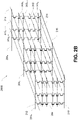
- Figure 2B is another schematic of a portion of an array of memory cells 200B as could be used in a memory of the type described with reference to Figures 1A , e.g., as a portion of array of memory cells 104. Like numbered elements in Figure 2B correspond to the description as provided with respect to Figure 2A .
- Figure 2B provides additional detail of one example of a three-dimensional NAND memory array structure.
- the three-dimensional NAND memory array 200B may incorporate vertical structures which may include semiconductor pillars where a portion of a pillar may act as a channel region of the memory cells of NAND strings 206.
- the NAND strings 206 may be each selectively connected to a bit line 204 0 -204 M by a select transistor 212 (e.g., that may be drain select transistors, commonly referred to as select gate drain) and to a common source 216 by a select transistor 210 (e.g., that may be source select transistors, commonly referred to as select gate source).
- Multiple NAND strings 206 might be selectively connected to the same bit line 204.
- Subsets of NAND strings 206 can be connected to their respective bit lines 204 by biasing the select lines 215 0 -215 L to selectively activate particular select transistors 212 each between a NAND string 206 and a bit line 204.
- the select transistors 210 can be activated by biasing the select line 214.
- Each word line 202 may be connected to multiple rows of memory cells of the memory array 200B. Rows of memory cells that are commonly connected to each other by a particular word line 202 may collectively be referred to as tiers.
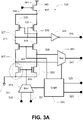
- FIG 3A is a schematic of a differential storage device 300.
- the differential storage includes a first non-volatile memory cell 301 and a second non-volatile memory cell 303 connected in parallel.
- Each of the non-volatile memory cells 301/303 may have a structure of the type described with reference to the memory cells 208 of Figure 2A , e.g., each non-volatile memory cell 301/303 may include a field-effect transistor (e.g., an n-type field effect transistor or nFET) having a data-storage structure that can determine a data state of that memory cell through changes in threshold voltage.
- a field-effect transistor e.g., an n-type field effect transistor or nFET
- the gate (e.g., control gate) of the non-volatile memory cell 301 is connected to the gate (e.g., control gate) of the non-volatile memory cell 303.
- the non-volatile memory cell 301 is connected in series between a node 307 and a voltage node 317, such as a reference voltage node configured to receive a reference voltage such as Vss, ground or 0V, for example.
- the non-volatile memory cell 303 is connected in series between a node 309 and the voltage node 317.
- the non-volatile memory cell 301 may have a first source/drain connected to the voltage node 317 and a second source/drain connected to the node 307, while the non-volatile memory cell 303 may have a first source/drain connected to the voltage node 317 and a second source/drain connected to the node 309.
- the differential storage device 300 may facilitate storing a digit (e.g., bit) of data determined in response to a difference in current flow through each of the non-volatile memory cells 301/303 of the pair of gate-connected non-volatile memory cells.
- the differential storage device 300 includes an isolation gate (e.g., nFET) 311 having a first source/drain connected to the node 307 and a second source/drain connected to the node 327, and an isolation gate (e.g., nFET) 313 having a first source/drain connected to the node 309 and a second source/drain connected to the node 329.
- the gate (e.g., control gate) of the nFET 311 may be connected to the gate (e.g., control gate) of the nFET 313.
- the differential storage device 300 may further include a p-type field-effect transistor (pFET) 333 having a first source/drain connected to the node 327 and a second source/drain connected to the node 337, and a pFET 335 having a first source/drain connected to the node 329 and a second source/drain connected to the node 337.
- the gate (e.g., control gate) of the pFET 333 may be connected to the node 329 while the gate (e.g., control gate) of the pFET 335 may be connected to the node 327.
- the differential storage device 300 may further include a pFET 341 having a first source/drain connected to the node 337 and a second source/drain connected to the voltage node 349.
- the voltage node 349 may be configured to receive a supply voltage, such as Vcc or other voltage greater than the voltage level of the voltage node 317.
- the supply voltage may be a voltage (e.g., one of the voltages) used to access the array of memory cells.
- the gate (e.g., control gate) of the pFET 341 may be connected to the control signal node 339.
- the differential storage device 300 may further include an output buffer, such as inverter 331.
- the inverter 331 has an input connected to the node 327, and an output connected to the buffer output node 345.
- the differential storage device may further include a multiplexer 315 and a multiplexer 343.
- the multiplexer 315 may be connected to receive a plurality of voltage signals, such as voltage signals received from voltage signal nodes 319 and 321.
- the voltage signal node 319 may be configured to receive a first voltage, such as a read voltage, and the voltage signal node 321 may be configured to receive a second voltage, such as a program voltage.
- the output of the multiplexer 315 may be connected to the gates of the non-volatile memory cells 301 and 303.
- the multiplexer 343 may be configured to receive a voltage signal, such as a voltage signal from voltage signal node 347.
- the voltage signal node 347 may be configured to receive a voltage, e.g., a drain voltage configured to enable programming of one of the non-volatile memory cells 301 or 303 as described below.
- the differential storage device 300 may further include logic 305 for access of the differential storage device 300.
- the logic 305 may be responsive to a plurality of control signals, such as control signals received from control signal nodes 323 and 325.
- Control signal node 323 may be configured to receive one or more control signals indicative of a data value (e.g., a digit of data) of a memory cell.
- the data value of the memory cell may represent one page (e.g., one digit) of data of an MLC memory cell. For example, during programming of an upper page of data to a memory cell configured to store two pages of data, the data value of the lower page of data may be stored (e.g., in a cache register or other temporary storage location).
- the control signal node 323 may be configured to receive a control signal indicative of the data value of the lower page of data, and may further be configured to receive a control signal that is a complement of the control signal indicative of the data value of the lower page of data.
- Control signal node 325 may be configured to receive one or more control signals indicative of whether a power fail is indicated.
- the control signal node 325 may be configured to receive a control signal indicative of whether a power fail is indicated, and may further be configured to receive a control signal that is a complement of the control signal indicative of whether a power fail is indicated.
- the logic 305 may further be responsive to one or more other control signals.
- the multiplexer 315 may be responsive to one or more control signals from the logic 305 to select one of its input voltage signals to apply to the gates of the non-volatile memory cells 301 and 303.
- the multiplexer 343 may be responsive to one or more control signals from the logic 305 to apply its received voltage to a select one of the nodes 307 and 309 for application to the second source/drain of the non-volatile memory cell 301 or the second source/drain of the non-volatile memory cell 303, respectively.
- the logic 305 may further be configured to provide a control signal to the gates of the nFETs 311 and 313 to selectively activate nFETS 311 and 313, such as during a read operation on the differential storage device 300, or deactivate nFETs 311 and 313, such as during a programming operation on one of the non-volatile memory cells 301 or 303.
- the differential storage device 300 it can be seen that if the non-volatile memory cell 301 is unprogrammed (e.g., having a threshold voltage at an initial value) and the non-volatile memory cell 303 is programmed (e.g., having a threshold voltage greater than the initial value), the unprogrammed non-volatile memory cell 301 may be activated in response to a voltage level applied to its gate while the programmed non-volatile memory cell 303 may remain deactivated in response to that same voltage level. By activating the nFETs 311 and 313, and activating the pFET 341, current may flow through the non-volatile memory cell 301 while the non-volatile memory cell 303 may inhibit such current flow.
- the node 327 will have a logic low level, thus activating the pFET 335. This will bring node 329 to a logic high level, thus deactivating the pFET 333 and maintaining the node 327 at the logic low level.
- the buffer output node 345 may have a logic high level as a result.
- the non-volatile memory cell 301 is programmed and the non-volatile memory cell 303 is unprogrammed, activating the nFETs 311 and 313, and activating the pFET 341, may result in current flow through the non-volatile memory cell 303 while the non-volatile memory cell 301 may inhibit such current flow.
- the node 329 will have a logic low level, thus activating the pFET 33. This will bring node 327 to a logic high level, thus deactivating the pFET 333 and maintaining the node 327 at the logic high level.
- the buffer output node 345 may have a logic low level as a result.
- the nFETs 311 and 313 are deactivated to isolate the non-volatile memory cells 301 and 303 from the pFETs 333 and 335.
- the voltage level of the voltage signal node 321 is applied to the gates of both non-volatile memory cells 301 and 303, while the voltage level of the voltage signal node 347 is applied to the second source/drain of the non-volatile memory cell 301 or 303 selected for programming.
- the voltage level of the voltage signal node 321 may be about 15V while the voltage level of the voltage signal node 347 may be about 5V.
- the non-volatile memory cells 301 and 303 would both be activated, the non-volatile memory cell 301 or 303 receiving the voltage level of the voltage signal node 321 at its second source/drain (e.g., at node 307 or 309, respectively) would be conducting current to the voltage node 317 and charge carriers (e.g., electrons) could tunnel or otherwise be injected into the data-storage node of that non-volatile memory cell.
- the remaining non-volatile memory cell 301 or 303 would have its second source/drain connected to the voltage node 317, and may not experience an increase of electrons in its data-storage node, such that it would remain in its initial (e.g., erased) state.
- the non-volatile memory cells 301 and 303 might optionally be formed in an isolated well structure 302, e.g., a semiconductor structure isolated from bodies of remaining transistors of the differential storage device 300.
- the bodies of the non-volatile memory cells 301 and 303 might be biased at an erase voltage, e.g., 20V, while the control gates of the non-volatile memory cells 301 and 303 are biased at a lower voltage expected to remove charge from data-storage structures of the non-volatile memory cells 301 and 303, e.g., Vss. This could facilitate erasure of the non-volatile memory cells 301 and 303 while mitigating detrimental effect on remaining components of the differential storage device 300.
- non-volatile memory cells 301 and 303 of the differential storage device 300 are depicted as distinct devices, non-volatile memory cells may utilize structures similar to (e.g., the same as) the NAND strings shown in Figure 2A .
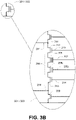
- Figure 3B is a schematic of an alternate structure that could be used as a non-volatile memory cell 301 or 303 of the differential storage device 300. As shown in Figure 3B , the non-volatile memory cell 301 or 303 may be represented as a NAND string 206.
- the NAND string 206 could be modified to include only one memory cell 208 between the select gates 210 and 212, or it could include additional memory cells 208 in series.
- the output of the multiplexer 315 might be applied to only one of the word lines 202, or it might be applied to more than one, and possibly all, of the word lines 202 such that multiple memory cells 208 in series may act as a single non-volatile memory cell 301 or 303.
- isolation gates e.g., nFETs
- the NAND string 206 could be isolated from remaining circuitry of the differential storage device 300.
- the non-volatile memory cell 301 or 303 could be erased using the same mechanisms discussed with respect to Figure 2A .
- the logic 305 could be modified accordingly to activate the nFETs 351 and 353 whenever access to the non-volatile memory cells 301 or 303 is desired.
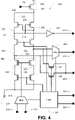
- Figure 4 is a schematic of a differential storage device 400.
- the differential storage device 400 may differ from the differential storage device 300 in the addition of isolation gates (e.g., nFETs) 461 and 463, and pFETs 465 and 467.
- the nFET 461 is connected in series between the non-volatile memory cell 301 and the voltage node 317, while the nFET 463 is connected in series between the non-volatile memory cell 303 and the voltage node 317.
- the nFETs 461 and 463 have their gates (e.g., control gates) connected together, and are responsive to control signals from the logic 305.
- the pFET 465 has a first source/drain connected to the node 307 and a second source/drain connected to the voltage signal node 469.
- the pFET 467 has a first source/drain connected to the node 309 and a second source/drain connected to the voltage signal node 469.
- the pFETs 465 and 467 have their gates (e.g., control gates) connected together, and are responsive to control signals from the logic 305.
- the voltage signal node 469 may be configured to receive an erase voltage.
- the erase voltage may be some voltage level that is higher than the voltage level of the voltage signal node 319 that when both are applied to nodes 307/309 and the gates of the non-volatile memory cells 301/303, respectively, and the nFETs 461 and 463 are deactivated (e.g., to float the remaining source/drain of each non-volatile memory cell 301/303), the voltage drop from the channel of the non-volatile memory cells 301/303 to the gates of the non-volatile memory cells 301/303 is sufficient to remove charge from the data-storage structure of the non-volatile memory cells 301/303.
- the erase voltage could be applied (e.g., selectively applied) to the voltage signal node 347 such that the multiplexer 343 could be used to selectively apply the erase voltage to a single node 307 or 309 to erase only the non-volatile memory cell 303 or 303 that had previously been programmed. This might be useful in mitigating any issues of over erasing a memory cell. Note that during an erase operation on the differential storage device 400, the nFETs 311 and 313 may also be deactivated.
- the multiplexer 315 might be configured to have a third input connected to the voltage node 317, such that a reference voltage (e.g., Vss, ground or 0V) could be applied to the gates of the non-volatile memory cells 301 and 303, which might facilitate a reduction in the voltage level of the erase voltage relative to using the voltage level of the voltage signal node 319.
- a reference voltage e.g., Vss, ground or 0V
- FIG. 5 is a schematic of a differential storage device 500.
- the differential storage device 500 may differ from the differential storage device 300 in the replacement of the multiplexer 343 with a switch 343' such that only one of the nodes 307 and 309 is selectively connected to the voltage signal node 347.
- the pFETs 333' and 335' may have differing W/L ratios or otherwise configured to have different conductance at a particular gate voltage.
- the W/L ratio of the pFET 335' may be greater than the W/L ratio of the pFET 333', such that its conductance at a particular gate voltage is less than the conductance of the pFET 333'.
- a default logic level of the node 327 may be a logic low level if both non-volatile memory cells 301 and 303 are unprogrammed, and a logic high level if the non-volatile memory cell 301 is programmed. Programming and erasing of the non-volatile memory cell 301 in this example can be performed as discussed with reference to Figures 3A , 3B and 4 , with any apparent modifications in structure as discussed with reference to Figures 3B or 4 .
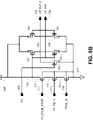
- Figures 6A-6E collectively depict a schematic of a specific implementation of a differential storage device of the type described with reference to Figure 3A .
- the nFETs 311 and 313 may be high-voltage nFETs sufficient to protect the pFETs 333 and 335 from the voltages utilized during programming and/or erasing of the non-volatile memory cells 301 and 303.
- the inverter 331 may include a pFET 671 and an nFET 673 connected in series between the node 337 and the voltage node 317.
- the non-volatile memory cell 301 might have a first source/drain connected to the voltage node 704 and a second source/drain connected to the node 307, while the non-volatile memory cell 303 might have a first source/drain connected to the voltage node 704 and a second source/drain connected to the node 309.
- the voltage node 704 might be configured to receive the voltage V_SRC, which may be a same voltage as received by the voltage node 317.
- the bodies of the non-volatile memory cells 301 and 303 may be connected to the voltage node 702, which might represent the isolated well structure 302 of Figure 3A , configured to receive the voltage V_ATUB.
- the voltage V ATUB may be a same voltage as received by the voltage node 317 during programming or reading the differential storage device, and may be an erase voltage, e.g., 20V, during an erase operation on the non-volatile memory cells 301 and 303.
- the multiplexer 315 may include pFETs (e.g., high-voltage pFETs) 683 and 685 connected in series between the voltage nodes 319 and 321.
- the gate of the pFET 683 may be connected to the control signal node 687 to receive a control signal DIS_VREF from the logic 305 of Figure 3A
- the gate of the pFET 685 may be connected to the control signal node 689 to receive a control signal DIS_VPP from the logic 305 of Figure 3A .
- the voltage node 319 may be the output of a voltage divider including nFETs 691, 693 and 695 connected in series between the voltage node 349 (e.g., selectively connected through pFET 341) and the voltage node 317.
- the nFET 695 may be a non-volatile memory cell 695 to permit adjustment of the voltage level of the voltage node 319.
- the voltage level of the voltage node 319 may be adjusted to a level sufficient to activate an unprogrammed non-volatile memory cell 301 or 303, and insufficient to activate a programmed non-volatile memory cell 301 or 303.
- the multiplexer 343 may include pFETs (e.g., high-voltage pFETs) 675 and 677, each connected in series between the voltage signal node 347 and their respective node 307 or 309.
- the gate of the pFET 675 may be connected to the control signal node 679 to receive a control signal PROG_A_N from the logic 305 of Figure 3A
- the gate of the pFET 677 may be connected to the control signal node 681 to receive a control signal PROG_ ⁇ _N from the logic 305 of Figure 3A .
- the pFETs 675 and 677 of the multiplexer 343 might instead be nFETs, e.g., high-voltage nFETs.
- the differential storage device of Figures 6A-6E may further include nFETs 697 and 701, and pFETs 699 and 703.
- the nFETs 697 and 701 are each connected in series with the pFETs 699 and 703 between the voltage node 349 and the voltage node 317, and are connected in parallel with each other.
- the control gates of the nFET 697 and the pFET 699 are each connected to the control signal node 705 to receive a control signal PROG_A, and the control gates of the nFET 701 and the pFET 703 are each connected to the control signal node 707 to receive a control signal PROG B.
- the nFETs 697 and 701, and the pFETs 699 and 703, may form a portion of the logic 305 of Figure 3A .
- Figure 6B depicts a portion of the differential storage device that may provide such decoupling.
- the differential storage device may further include nFETs 717, 719 and 721 connected in series between a voltage node 349' and a voltage node 317'.
- the voltage node 349' may be the same as the voltage node 349 of Figure 6A or otherwise configured to receive the same voltage level.
- the voltage node 317' may be the same as the voltage node 317 of Figure 6A or otherwise configured to receive the same voltage level.
- the gate of the nFET 717 is connected to the control signal node 711 to receive a control signal LP DQ N VALID
- the gate of the nFET 719 is connected to the control signal node 713 to receive a control signal LP_DQ_N
- the gate of the nFET 721 is connected to the control signal node 715 to receive a control signal PF_AIL_N.
- the control signal LP _DQ_N_VALID may have a logic high level when the data value of the prior page data to be stored by the differential storage device is valid
- the control signal LP_DQ_N may represent the complement of the data value of the prior page data
- the control signal PFAIL_N may have a logic high level to indicate a normal power level.
- Each of these control signals might be received from the control logic 116 of Figure 1A , for example.
- the nFETs 725 and 731, and the pFETs 727 and 729 may form a latch configured as a pair of cross-coupled inverters between the voltage node 349' and the voltage node 317', having an input (e.g., the gates of the nFET 725 and the pFET 727) connected to node 741.
- the input of the latch is further connected to node 745 between the nFET 731 and the pFET 729.
- the node 743 between the nFET 725 and the pFET 727 is connected to the gates of the nFET 731 and the pFET 729, as well as the output node 737, providing a control signal LP_BUF_N that may be representative of the complement of the data value of the prior page data.
- the node 745 is connected to the output node 739, providing a control signal LP_BUF that may be representative of the data value of the prior page data.
- An nFET 723 might be connected between the node 743 and the voltage node 317' for selectively precharging the latch, e.g., setting the output node 737 to a logic low level and the output node 739 to a logic high level.
- the nFET 723 may have its gate connected to the control signal node to receive a control signal PC, indicative of whether such a precharge is desired, and may be received from the control logic 116 of Figure 1A .
- Figure 6C depicts a level shifter of the differential storage device that may be a portion of the logic 305 of Figure 3A , and may be configured to generate an output control signal having a voltage level of the voltage node 777, e.g., configured to receive a voltage VCC_VDRAIN.
- VCC_VDRAIN may be selected to have a voltage level sufficient to program a non-volatile memory cell 301 or 303 when applied to its drain as previously described.
- the level shifter of Figure 6C may be a portion of the logic 305 of Figure 3A .
- pFET 751, nFET 753 and nFET 755 are connected in series between the voltage node 349" and a voltage node 317".
- the voltage node 349" may be the same as the voltage node 349 of Figure 6A or otherwise configured to receive the same voltage level.
- the voltage node 317" may be the same as the voltage node 317 of Figure 6A or otherwise configured to receive the same voltage level.
- the gate of the pFET 751 is connected to the control signal node 749 to receive a control signal PC_N
- the gate of the nFET 753 is connected to the control signal node 737 to receive the control signal LP_BUF_N
- the gate of the nFET 755 is connected to the control signal node 747 to receive a control signal PFAIL.
- the control signal PC_N may be the complement of the control signal PC
- the control signal PFAIL may be the complement of the control signal PFAIL_N, e.g., having a logic high level to indicate a power loss, and each of these control signals might be received from the control logic 116 of Figure 1A , for example.
- the control signals PFAIL and PFAIL_N might be output signals of a voltage level detection circuit of the control logic 116 that are often used to detect when a supply voltage , such as Vcc, falls below some minimum threshold value.
- a supply voltage Vcc may have a specification calling for a nominal value of 3.3V, with a desired (e.g., acceptable) range of 2.7V-3.6V.
- a voltage detection circuit might be configured to generate the control signal PFAIL having a logic high level if the voltage level of Vcc falls below some threshold value (e.g., some minimum threshold value), such as 2.5V for this example.
- some threshold value e.g., some minimum threshold value
- Adjustments to the threshold value might be warranted to permit operation of a differential storage device without connection to an auxiliary energy storage device.
- the threshold value might be increased, and may be increased to some level within the desired range of threshold voltages, e.g., within the range of 2.7V-3.6V in this example. While this might result in unnecessary programming of the differential storage device in response to a dip in power, the non-volatile memory cells of the differential storage device could be erased if the supply voltage returned to its nominal value.
- the level shifter of Figure 6C may further include an nFET (e.g., high-voltage nFET) 757 having a first source/drain connected to a source/drain between the pFET 751 and the nFET 753.
- the level shifter of Figure 6C may further include an nFET (e.g., high-voltage nFET) 763 and a pFET (e.g., high-voltage pFET) 761 connected in series between the voltage node 777 and the voltage node 317".
- the nFET 763 and pFET 761 have their gates connected to a second source/drain of the nFET 757, and to a source/drain of the pFET (e.g., high-voltage pFET) 759 having a second source/drain connected to the voltage node 777.
- a source/drain of the pFET e.g., high-voltage pFET
- the level shifter of Figure 6C may further include an nFET (e.g., high-voltage nFET) 767 and a pFET (e.g., high-voltage pFET) 765 connected in series between the voltage node 777 and the voltage node 317".
- the nFET 763 and pFET 761 have their gates connected to the node 769 and to the gate of the pFET 759.
- the node 769 is connected to the control signal node 705 to provide the control signal PROG A
- the node 771 is connected to the control signal node 681 to provide the control signal PROG_A_N, e.g., the complement of the control signal PROG A.
- Figure 6D depicts another level shifter of the differential storage device that may be a portion of the logic 305 of Figure 3A , and may be configured to generate an output control signal having the voltage level VCC_VDRAIN.
- the structure of Figure 6D is depicted to be the same as the structure of Figure 6C , and will thus only with respect to the differences between the inputs and outputs.
- the level shifter of Figure 6D is configured to receive the control signal LP_BUF from control signal node 739.
- the level shifter of Figure 6D provides the control signals PROG_B and PROG_B_N at control signal nodes 707 and 679, respectively.
- the control signal PROG_B is generally the complement of the control signal PROG A
- the control signal PROG_B_N is generally the complement of the control signal PROG B.
- the level shifter of Figure 6D may be a portion of the logic 305 of Figure 3A .
- Figure 6E depicts another level shifter of the differential storage device that may be a portion of the logic 305 of Figure 3A , and may be configured to generate an output control signal having the voltage level VCC_VPP.
- the structure of Figure 6E is depicted to be the same as the structure of Figure 6C , and will thus only with respect to the differences between the inputs and outputs.
- the level shifter of Figure 6D is configured to receive the voltage level of the voltage node 783 (e.g., at the gate of the nFET 753).
- the voltage node 783 may be configured to receive the same voltage level as the voltage node 349 of Figure 6A .
- the level shifter of Figure 6E instead of providing the control signals PROG A and PROG_A_N at control signal nodes 705 and 681, respectively, the level shifter of Figure 6E provides the control signals DIS_VREF and DIS_VPP at control signal nodes 687 and 689, respectively.
- the control signal DIS_VPP is generally the complement of the control signal DIS_VREF.
- the level shifter of Figure 6E may be a portion of the logic 305 of Figure 3A .
- Table 1 may illustrate representative values of the various control signals of Figures 6A-6E during normal operation and when a power loss is detected.
- "0” represents a logic low level
- "1” represents a logic high level
- "X” represents "do not care” values of the logic levels.
- the level shifters of Figures 6C-6E will generate (e.g., automatically generate) values of the control signals PROG_A, PROG_A_N, PROG B, PROG_B_N, DIS VREF and DIS_VPP representative of the values of the control signals LP_BUF and LP_BUF_N indicative of the data value of the prior page data to be stored.
- the nFETs 311 and 313 will be deactivated in response to connecting their gates to the voltage node 317, the voltage VCC_VDRAIN will be applied to a select one of the nodes 307 or 309, and the voltage VCC_VPP will be applied to the gates of the non-volatile memory cells 301 and 303.
- the non-volatile memory cell 301 or 303 receiving the voltage VCC_VDRAIN at its second source/drain while its first source/drain is connected to the voltage node 317 and its gate is connected to receive the voltage VCC_VPP will be expected to accumulate charge on its data-storage structure, thus increasing its threshold voltage.
- Figure 7 is a flowchart of a method of operating a memory containing a differential storage device.
- information indicative of a data value stored in a particular memory cell is obtained.
- the information may be indicative of a data value of a prior (e.g., lower) page of data stored in a memory cell that is intended to undergo a programming operation to further store a subsequent (e.g., upper) page of data to that memory cell.
- the information indicative of the data value may be obtained directly from a data source, such as a cache register of a memory device, or it may be decoupled from the data source and stored in a latch, for example.
- the information indicative of the data value may be represented by one or more control signals.
- a first digit (e.g., bit) of data may be programmed to the memory cell prior to programming its second digit (e.g., bit) of data.
- the second digit of data e.g., bit
- the information indicative of the data value stored in the particular memory cell may be obtained by reading the first digit of data from the particular memory cell prior to performing the programming operation to store the second digit of data. Alternatively, the information indicative of the data value stored in the particular memory cell may still be available from the prior programming operation.
- additional data is programmed to the particular memory cell.
- the subsequent page (e.g., second digit) of data may be programmed to the memory cell.
- one memory cell of a pair of gate-connected non-volatile memory cells of a differential storage device may be programmed responsive to the information indicative of the data value stored in the particular memory cell.
- the prior page data of each memory cell of that logical page of memory cells may be stored to the pair of gate-connected non-volatile memory cells of their respective differential storage device in the event of a power loss.
- storing the prior page data of a memory cell to a pair of gate-connected non-volatile memory cells does not necessarily require programming of a memory cell of that pair of gate-connected non-volatile memory cells, e.g., where one data value is indicated by the programming of one of the memory cells, and the other data value is indicated by the lack of programming either of the memory cells.
- the voltage nodes of the differential storage device may be devoid of connection to an auxiliary energy storage device.
Landscapes
- Engineering & Computer Science (AREA)
- Microelectronics & Electronic Packaging (AREA)
- Computer Hardware Design (AREA)
- Computer Security & Cryptography (AREA)
- Power Engineering (AREA)
- Read Only Memory (AREA)
Claims (15)
- Gerät, umfassend:ein Array aus nichtflüchtigen Speicherzellen (104); undeine Differenzspeichervorrichtung (300, 400, 500), die so konfiguriert ist, dass sie Informationen empfängt, die einen Datenwert angeben, der in einer bestimmten Speicherzelle (208) des Arrays aus nichtflüchtigen Speicherzellen (104) gespeichert ist, die für eine Programmieroperation ausgewählt ist, die der Differenzspeichervorrichtung (300, 400, 500), umfassend:eine erste nichtflüchtige Speicherzelle (301), die zwischen einem ersten Isolationsgate (311) und einem ersten Spannungsknoten (317, 704) verbunden ist, der so konfiguriert ist, dass er einen ersten Spannungspegel empfängt;eine zweite nichtflüchtige Speicherzelle (303), die zwischen einem zweiten Isolationsgate (313) und einem ersten Spannungsknoten (317, 704) verbunden ist, wobei ein Gate der zweiten nichtflüchtigen Speicherzelle (303) mit einem Gate der ersten nichtflüchtigen Speicherzelle (301) verbunden ist;einen zweiten Spannungsknoten (349), der dazu konfiguriert ist, einen zweiten Spannungspegel zu empfangen, der höher als der erste Spannungspegel ist, wobei der zweite Spannungsknoten (349) selektiv mit dem ersten Isolationsgate (311) verbunden ist und selektiv mit dem zweiten Isolationsgate (313) verbunden ist, wobei das erste Isolationsgate (311) zwischen dem zweiten Spannungsknoten (349) und der ersten nichtflüchtigen Speicherzelle (301) liegt und wobei das zweite Isolationsgate (313) zwischen dem zweiten Spannungsknoten (349) und der zweiten nichtflüchtigen Speicherzelle (303) liegt; undLogik (305), die auf eine Angabe eines Leistungsverlusts für das Gerät und die Informationen reagiert, die den in der bestimmten Speicherzelle (208) gespeicherten Datenwert angeben;wobei die Logik (305) so konfiguriert ist, um zu bewirken, dass das erste Isolationsgate (311) und das zweite Isolationsgate (313) als Reaktion auf die Angabe eines Leistungsverlusts an das Gerät mit einem bestimmten Logikpegel unabhängig von einem Logikpegel der Informationen, die den in der bestimmten Speicherzelle (208) gespeicherten Datenwert angeben, deaktiviert werden;wobei die Logik (305) ferner konfiguriert ist, um zu bewirken, dass ein dritter Spannungspegel, der höher als der zweite Spannungspegel ist, an Gates der ersten nichtflüchtigen Speicherzelle (301) und der zweiten nichtflüchtigen Speicherzelle (303) angelegt wird, als Reaktion auf die Angabe eines Leistungsverlusts an das Gerät, das ihren bestimmten Logikpegel aufweist, unabhängig des Logikpegels der Informationen, die den in der bestimmten Speicherzelle (208) gespeicherten Datenwert angeben;wobei die Logik (305) ferner konfiguriert ist, um zu bewirken, dass ein vierter Spannungspegel, der niedriger als der dritte Spannungspegel und höher als der zweite Spannungspegel ist, an einen Knoten (307) zwischen der ersten nichtflüchtigen Speicherzelle (301) und dem ersten Isolationsgate (311) angelegt wird, als Reaktion auf die Angabe eines Leistungsverlusts an das Gerät mit seinem bestimmten Logikpegel und die Informationen, die den in der bestimmten Speicherzelle (208) gespeicherten Datenwert angeben, einen bestimmten Logikpegel aufweisen; undwobei die Logik (305) ferner konfiguriert ist, um zu bewirken, dass der erste Spannungspegel an den Knoten (307) zwischen der ersten nichtflüchtigen Speicherzelle (301) und dem ersten Isolationsgate (311) angelegt wird, als Reaktion auf die Angabe eines Leistungsverlusts an das Gerät mit seinem bestimmten Logikpegel und die Informationen, die den in der bestimmten Speicherzelle (208) gespeicherten Datenwert angeben, einen Logikpegel unterschiedlich als sein bestimmter Logikpegel aufweisen.
- Gerät nach Anspruch 1, ferner umfassend:
eine jeweilige Differenzspeichervorrichtung (300, 400, 500) für jede verbleibende Speicherzelle des Arrays von nichtflüchtigen Speicherzellen (104), die für die Programmieroperation ausgewählt wurden. - Gerät nach Anspruch 2, wobei die bestimmte Speicherzelle ( 208 ) und für jede verbleibende Speicherzelle ( 208 ) des Arrays von nichtflüchtigen Speicherzellen ( 104 ), die für die Programmieroperation ausgewählt wurden, gemeinsam eine logische Seite von Speicherzellen (208) des Arrays aus nichtflüchtigen Speicherzellen (104) umfassen.
- Gerät nach Anspruch 2, wobei jede jeweilige Differentialspeichervorrichtung (300, 400, 500) umfasst:eine erste nichtflüchtige Speicherzelle (301), die zwischen einem ersten Isolationsgate (311) und dem ersten Spannungsknoten (317, 704) verbunden ist;eine zweite nichtflüchtige Speicherzelle (303), die zwischen einem zweiten Isolationsgate (313) und einem ersten Spannungsknoten (317, 704) verbunden ist, wobei ein Gate der zweiten nichtflüchtigen Speicherzelle (303) mit einem Gate der ersten nichtflüchtigen Speicherzelle (301) verbunden ist;einen zweiten Spannungsknoten (349), der dazu konfiguriert ist, einen zweiten Spannungspegel zu empfangen, der höher als der erste Spannungspegel ist, wobei der zweite Spannungsknoten (349) selektiv mit dem ersten Isolationsgate (311) verbunden ist und selektiv mit dem zweiten Isolationsgate (313) verbunden ist, wobei das erste Isolationsgate (311) zwischen dem zweiten Spannungsknoten (349) und der ersten nichtflüchtigen Speicherzelle (301) liegt und wobei das zweite Isolationsgate (313) zwischen dem zweiten Spannungsknoten (349) und der zweiten nichtflüchtigen Speicherzelle (303) liegt; undLogik (305), die auf die Angabe eines Leistungsverlusts an das Gerät und Informationen reagiert, die einen in seiner jeweiligen Speicherzelle (208) gespeicherten Datenwert angeben;wobei die Logik (305) so konfiguriert ist, um zu bewirken, dass das erste Isolationsgate (311) und das zweite Isolationsgate (313) als Reaktion auf die Angabe eines Leistungsverlusts an das Gerät mit seinem bestimmten Logikpegel unabhängig von einem Logikpegel der Informationen, die den in der bestimmten Speicherzelle (208) gespeicherten Datenwert angeben, deaktiviert werden;wobei die Logik (305) ferner konfiguriert ist, um zu bewirken, dass der dritte Spannungspegel an Gates der ersten nichtflüchtigen Speicherzelle (301) und der zweiten nichtflüchtigen Speicherzelle (303) angelegt wird, als Reaktion auf die Angabe eines Leistungsverlusts an das Gerät mit seinem bestimmten Logikpegel unabhängig von dem Logikpegel der Informationen, die den in seiner jeweiligen Speicherzelle (208) gespeicherten Datenwert angeben;wobei die Logik (305) ferner konfiguriert ist, um zu bewirken, dass der vierte Spannungspegel an einen Knoten (307) zwischen der ersten nichtflüchtigen Speicherzelle (301) und dem ersten Isolationsgate (311) angelegt wird, als Reaktion auf die Angabe eines Leistungsverlusts an das Gerät mit seinem bestimmten Logikpegel und die Informationen, die den in der bestimmten Speicherzelle (208) gespeicherten Datenwert angeben, einen bestimmten Logikpegel aufweisen; undwobei die Logik (305) ferner konfiguriert ist, um zu bewirken, dass der erste Spannungspegel an den Knoten (307) zwischen der ersten nichtflüchtigen Speicherzelle (301) und dem ersten Isolationsgate (311) angelegt wird, als Reaktion auf die Angabe eines Leistungsverlusts an das Gerät mit seinem bestimmten Logikpegel und die Informationen, die den in der bestimmten Speicherzelle (208) gespeicherten Datenwert angeben, einen Logikpegel unterschiedlich als sein bestimmter Logikpegel aufweisen.
- Gerät nach Anspruch 1, wobei die Angabe eines Leistungsverlusts an das Gerät eine Angabe eines Leistungsverlusts für einen Abschnitt des Geräts umfasst, der das Array aus nichtflüchtigen Speicherzellen (104) enthält.
- Gerät nach Anspruch 1, wobei die Logik (305) ferner konfiguriert ist um:zu veranlassen, dass der vierte Spannungspegel an einen Knoten (309) zwischen der zweiten nichtflüchtigen Speicherzelle (303) und dem zweiten Isolationsgate (313) angelegt wird, als Reaktion auf die Angabe eines Leistungsverlusts an das Gerät mit ihrer speziellen Logik Pegel und die Informationen, die den in der bestimmten Speicherzelle (208) gespeicherten Datenwert angeben, den bestimmten Logikpegel unterschiedlich als sein bestimmter Logikpegel aufweisen; undzu veranlassen, dass der erste Spannungspegel an den Knoten (309) zwischen der zweiten nichtflüchtigen Speicherzelle (303) und dem zweiten Isolationsgate (313) angelegt wird, als Reaktion auf die Angabe eines Leistungsverlusts an das Gerät mit seinem bestimmten Logikpegel und die Informationen, die den in der bestimmten Speicherzelle (208) gespeicherten Datenwert mit seinem bestimmten Logikpegel angeben.
- Gerät nach Anspruch 1, wobei das Gerät ein Fahrzeug ist.
- Gerätnach Anspruch 1, wobei die Logik (305), die auf die Angabe eines Leistungsverlusts an das Gerät reagiert, umfasst, dass die Logik auf komplementäre Steuersignale reagiert, die einen Spannungspegel einer Versorgungsspannung relativ zu einem Schwellenwert angeben und wobei die Logik, die auf die Informationen reagiert, die den in der bestimmten Speicherzelle (208) gespeicherten Datenwert angeben, die Logik umfasst, die auf komplementäre Steuersignale reagiert, die einen Logikpegel des in der bestimmten Speicherzelle gespeicherten Datenwerts angeben.
- Gerät nach Anspruch 1, wobei die Logik (305) ferner auf ein oder mehrere zusätzliche Steuersignale reagiert.
- Gerät nach Anspruch 1, wobei der Knoten (307) zwischen der ersten nichtflüchtigen Speicherzelle (301) und dem ersten Isolationsgate (311) ein erster Knoten (307) ist, wobei ein zweiter Knoten (309) zwischen dem zweiten Isolationsgate (313) und der zweiten nichtflüchtigen Speicherzelle (303) in Reihe verbunden ist, wobei die Angabe eines Leistungsverlusts an das Gerät mit einem bestimmten Logikpegel Informationen umfasst, die einen Spannungspegel einer Versorgungsspannung relativ zu einem Schwellenwert angeben, der angibt, dass der Spannungspegel der Versorgungsspannung niedriger als ein Schwellenwert ist, wobei die Versorgungsspannung für den Zugriff auf das Array aus nichtflüchtigen Speicherzellen (104) verwendet wird und wobei die Logik (305) umfasst:einen ersten Pegelumsetzer zum Erzeugen eines ersten Steuersignals und eines zweiten Steuersignals mit komplementären Logikpegeln als Reaktion auf die Informationen, die den Spannungspegel der Versorgungsspannung relativ zu dem Schwellwert angeben, und auf die Informationen, die den Datenwert einer Datenstelle von in der bestimmten Speicherzelle (208) gespeicherten Daten angeben;einen zweiten Pegelumsetzer zum Erzeugen eines dritten Steuersignals und eines vierten Steuersignals mit komplementären Logikpegeln als Reaktion auf die Informationen, die den Spannungspegel der Versorgungsspannung relativ zu dem Schwellenwert angeben, und auf die Informationen, die den Datenwert einer Datenstelle von in der bestimmten Speicherzelle (208) gespeicherten Daten angeben;einen dritten Pegelumsetzer zum Erzeugen eines fünften Steuersignals und eines sechsten Steuersignals mit komplementären Logikpegeln als Reaktion auf die Informationen, die den Spannungspegel der Versorgungsspannung relativ zu dem Schwellenwert angeben;wobei, wenn die Informationen, die den Spannungspegel der Versorgungsspannung relativ zu dem Schwellenwert angeben, angeben, dass der Spannungspegel der Versorgungsspannung höher als der Schwellenwert ist, das erste Steuersignal, das dritte Steuersignal und das fünfte Steuersignal jeweils einen ersten Logikpegel aufweisen und das zweite Steuersignal, das vierte Steuersignal und das sechste Steuersignal jeweils einen zweiten Logikpegel, der sich von dem ersten Logikpegel unterscheidet, aufweisen;wobei, wenn die Informationen, die den Spannungspegel der Versorgungsspannung relativ zu dem Schwellwert angeben, angeben, dass der Spannungspegel der Versorgungsspannung niedriger als der Schwellwert ist, und die Informationen, die den Datenwert der in der bestimmten Speicherzelle (208) gespeicherten Datenstelle angeben, angeben, dass der Datenwert der Datenstelle einen bestimmten Logikpegel aufweist, das zweite Steuersignal, das dritte Steuersignal und das sechste Steuersignal jeweils den ersten Logikpegel ausweisen und das erste Steuersignal, das vierte Steuersignal und das fünfte Steuersignal jeweils den zweiten Logikpegel aufweisen;wobei, wenn die Informationen, die den Spannungspegel der Versorgungsspannung relativ zu dem Schwellenwert angeben, angeben, dass der Spannungspegel der Versorgungsspannung niedriger als der Schwellenwert ist, und die Informationen, die den Datenwert der in der bestimmten Speicherzelle (208) gespeicherten Datenstelle angeben, angeben, dass der Datenwert der Datenstelle einen unterschiedlichen Logikpegel aufweist, das erste Steuersignal, das vierte Steuersignal und das sechste Steuersignal jeweils den ersten Logikpegel aufweisen, und das zweite Steuersignal, das dritte Steuersignal und das fünfte Steuersignal jeweils den zweiten Logikpegel aufweisen;wobei das erste Isolationsgate (311) und das zweite Isolationsgate (313) konfiguriert sind, um eine Gate-Spannung mit dem ersten Spannungspegel zu empfangen, wenn entweder das erste Steuersignal oder das dritte Steuersignal den zweiten Logikpegel aufwiest, und um eine Gate-Spannung mit dem zweiten Spannungspegel zu empfangen, wenn sowohl das erste Steuersignal als auch das dritte Steuersignal den ersten Logikpegel aufweisen;wobei die erste nichtflüchtige Speicherzelle (301) und die zweite nichtflüchtige Speicherzelle (303) dazu konfiguriert sind, eine Gate-Spannung mit einem fünften Spannungspegel zwischen dem ersten Spannungspegel und dem zweiten Spannungspegel zu empfangen, wenn das fünfte Steuersignal den ersten Logikpegel aufweist, und um eine Gate-Spannung mit dem dritten Spannungspegel zu empfangen, wenn das sechste Steuersignal den ersten Logikpegel aufweist;wobei der erste Knoten (307) so konfiguriert ist, dass er den vierten Spannungspegel empfängt, wenn das zweite Steuersignal den ersten Logikpegel aufweist; undwobei der zweite Knoten (309) konfiguriert ist, den vierten Spannungspegel zu empfangen, wenn das vierte Steuersignal den ersten Logikpegel aufweist.
- Gerät nach Anspruch 10, ferner umfassend:
einen ersten Multiplexer (343) mit einem Eingang (347), der zum Empfangen des vierten Spannungspegels konfiguriert ist, wobei der erste Multiplexer (343) auf das zweite Steuersignal und das vierte Steuersignal reagiert, um selektiv entweder den ersten Knoten (307) oder den zweiten Knoten (309) mit seinem Eingang (347) zu verbinden. - Gerät nach Anspruch 11, ferner umfassend:
einen zweiten Multiplexer (315) mit einem ersten Eingang (321), der zum Empfangen des dritten Spannungspegels konfiguriert ist, und einem zweiten Eingang (319), der zum Empfangen des fünften Spannungspegels konfiguriert ist, wobei der zweite Multiplexer (315) auf das fünfte Steuersignal und das sechste Steuersignal reagiert, um selektiv entweder den ersten Eingang (321) oder den zweiten Eingang (319) mit dem Gate jeder der ersten nichtflüchtigen Speicherzelle (301) und der zweiten nichtflüchtigen Speicherzelle (303) zu verbinden. - Gerät nach Anspruch 10, wobei der erste Logikpegel ein logisch niedriger Pegel ist und der zweite logische Pegel ein logisch hoher Pegel ist.
- Gerät nach Anspruch 13, wobei der bestimmte Logikpegel der erste Logikpegel ist und der unterschiedliche Logikpegel der zweite Logikpegel ist.
- Gerät nach Anspruch 10, wobei der zweite Spannungspegel ein Spannungspegel der Versorgungsspannung ist.
Applications Claiming Priority (2)
| Application Number | Priority Date | Filing Date | Title |
|---|---|---|---|
| US15/691,824 US10192626B1 (en) | 2017-08-31 | 2017-08-31 | Responding to power loss |
| PCT/US2018/043859 WO2019045921A1 (en) | 2017-08-31 | 2018-07-26 | RESPONSE TO LOSS OF POWER |
Publications (3)
| Publication Number | Publication Date |
|---|---|
| EP3676838A1 EP3676838A1 (de) | 2020-07-08 |
| EP3676838A4 EP3676838A4 (de) | 2021-05-19 |
| EP3676838B1 true EP3676838B1 (de) | 2022-11-23 |
Family
ID=65032700
Family Applications (1)
| Application Number | Title | Priority Date | Filing Date |
|---|---|---|---|
| EP18851275.0A Active EP3676838B1 (de) | 2017-08-31 | 2018-07-26 | Reaktion auf leistungsverlust |
Country Status (5)
| Country | Link |
|---|---|
| US (5) | US10192626B1 (de) |
| EP (1) | EP3676838B1 (de) |
| KR (1) | KR102316910B1 (de) |
| CN (1) | CN111095414B (de) |
| WO (1) | WO2019045921A1 (de) |
Families Citing this family (7)
| Publication number | Priority date | Publication date | Assignee | Title |
|---|---|---|---|---|
| US10373694B2 (en) * | 2017-08-31 | 2019-08-06 | Micron Technology, Inc. | Responding to power loss |
| US10192626B1 (en) * | 2017-08-31 | 2019-01-29 | Micro Technology, Inc. | Responding to power loss |
| US10468088B2 (en) | 2017-12-15 | 2019-11-05 | International Business Machines Corporation | Redundant voltage regulator for memory devices |
| JP6887457B2 (ja) * | 2019-03-01 | 2021-06-16 | 力晶積成電子製造股▲ふん▼有限公司Powerchip Semiconductor Manufacturing Corporation | 基準電圧発生回路及び不揮発性半導体記憶装置 |
| US12154634B2 (en) * | 2022-02-18 | 2024-11-26 | Infineon Technologies LLC | Data path circuit and method |
| US11929121B2 (en) * | 2022-03-09 | 2024-03-12 | Micron Technology, Inc. | Storing one data value by programming a first memory cell and a second memory cell |
| CN120895063B (zh) * | 2025-07-21 | 2026-03-31 | 深圳市华智胜科技有限公司 | 垂直堆叠多层电荷陷阱的三维闪存存储器阵列系统 |
Family Cites Families (55)
| Publication number | Priority date | Publication date | Assignee | Title |
|---|---|---|---|---|
| DE4342821C1 (de) | 1993-12-15 | 1994-12-15 | Sgs Thomson Microelectronics | Elektronische Speicherschaltung |
| US5914895A (en) | 1997-09-10 | 1999-06-22 | Cypress Semiconductor Corp. | Non-volatile random access memory and methods for making and configuring same |
| US6414873B1 (en) | 2001-03-16 | 2002-07-02 | Simtek Corporation | nvSRAM with multiple non-volatile memory cells for each SRAM memory cell |
| US6965524B2 (en) | 2002-03-19 | 2005-11-15 | O2Ic, Inc. | Non-volatile static random access memory |
| KR101066938B1 (ko) | 2003-06-17 | 2011-09-23 | 엔엑스피 비 브이 | 메모리 장치, 재구성 가능한 프로그래밍가능 논리 장치 및 fpga |
| JP2005064427A (ja) | 2003-08-20 | 2005-03-10 | Elpida Memory Inc | 不揮発性ランダムアクセスメモリおよびその製造方法 |
| KR100545212B1 (ko) | 2003-12-26 | 2006-01-24 | 동부아남반도체 주식회사 | 적층산화막 구조를 갖는 비휘발성 메모리소자 및 이를이용한 비휘발성 sram |
| US7283390B2 (en) | 2004-04-21 | 2007-10-16 | Impinj, Inc. | Hybrid non-volatile memory |
| US7164608B2 (en) | 2004-07-28 | 2007-01-16 | Aplus Flash Technology, Inc. | NVRAM memory cell architecture that integrates conventional SRAM and flash cells |
| KR100645044B1 (ko) * | 2004-09-17 | 2006-11-10 | 삼성전자주식회사 | 높은 신뢰도를 갖는 불 휘발성 메모리 장치의 프로그램 방법 |
| US7395452B2 (en) | 2004-09-24 | 2008-07-01 | Microsoft Corporation | Method and system for improved reliability in storage devices |
| JP4619367B2 (ja) | 2004-10-26 | 2011-01-26 | スパンション エルエルシー | 不揮発性記憶装置 |
| KR100682218B1 (ko) | 2005-05-30 | 2007-02-12 | 주식회사 하이닉스반도체 | 비휘발성 반도체 메모리 장치 |
| DE102005030142B3 (de) | 2005-06-28 | 2006-12-21 | Infineon Technologies Ag | Bistabile Kippstufe mit nichtflüchtiger Zustandsspeicherung |
| US7280397B2 (en) | 2005-07-11 | 2007-10-09 | Sandisk 3D Llc | Three-dimensional non-volatile SRAM incorporating thin-film device layer |
| US7369437B2 (en) * | 2005-12-16 | 2008-05-06 | Sandisk Corporation | System for reading non-volatile storage with efficient setup |
| US7606084B2 (en) * | 2006-06-19 | 2009-10-20 | Sandisk Corporation | Programming differently sized margins and sensing with compensations at select states for improved read operations in non-volatile memory |
| US7457155B2 (en) * | 2006-08-31 | 2008-11-25 | Micron Technology, Inc. | Non-volatile memory device and method having bit-state assignments selected to minimize signal coupling |
| US7760540B2 (en) | 2006-12-22 | 2010-07-20 | Cypress Semiconductor Corporation | Combination SRAM and NVSRAM semiconductor memory array |
| US7518916B2 (en) | 2006-12-22 | 2009-04-14 | Cypress Semiconductor Corporation | Method and apparatus to program both sides of a non-volatile static random access memory |
| US20080151654A1 (en) | 2006-12-22 | 2008-06-26 | Allan James D | Method and apparatus to implement a reset function in a non-volatile static random access memory |
| US7710776B2 (en) | 2006-12-27 | 2010-05-04 | Cypress Semiconductor Corporation | Method for on chip sensing of SONOS VT window in non-volatile static random access memory |
| US8817536B2 (en) | 2007-03-22 | 2014-08-26 | Cypress Semiconductor Corporation | Current controlled recall schema |
| US8516172B1 (en) * | 2007-08-30 | 2013-08-20 | Virident Systems, Inc. | Methods for early write termination and power failure with non-volatile memory |
| US7782674B2 (en) * | 2007-10-18 | 2010-08-24 | Micron Technology, Inc. | Sensing of memory cells in NAND flash |
| US7633798B2 (en) * | 2007-11-21 | 2009-12-15 | Micron Technology, Inc. | M+N bit programming and M+L bit read for M bit memory cells |
| US8194438B2 (en) | 2009-02-12 | 2012-06-05 | Seagate Technology Llc | nvSRAM having variable magnetic resistors |
| US8018768B2 (en) | 2009-08-18 | 2011-09-13 | United Microelectronics Corp. | Non-volatile static random access memory (NVSRAM) device |
| US8560765B2 (en) * | 2009-09-08 | 2013-10-15 | Lsi Corporation | Systems and methods for variable level use of a multi-level flash memory |
| US8824186B2 (en) | 2010-06-09 | 2014-09-02 | Radiant Technologies, Inc. | Embedded non-volatile memory circuit for implementing logic functions across periods of power disruption |
| WO2012001917A1 (ja) * | 2010-06-29 | 2012-01-05 | パナソニック株式会社 | 不揮発性記憶システム、メモリシステム用の電源回路、フラッシュメモリ、フラッシュメモリコントローラ、および不揮発性半導体記憶装置 |
| US8341500B2 (en) | 2010-08-31 | 2012-12-25 | Apple Inc. | Detecting corrupted data for a system having non-volatile memory |
| US8270224B2 (en) * | 2010-09-29 | 2012-09-18 | Micron Technology, Inc. | Voltage discharge circuits and methods |
| JP5886128B2 (ja) | 2011-05-13 | 2016-03-16 | 株式会社半導体エネルギー研究所 | 半導体装置 |
| US20130294161A1 (en) | 2012-05-07 | 2013-11-07 | Aplus Flash Technology, Inc. | Low-voltage fast-write nvsram cell |
| US20140082406A1 (en) * | 2012-09-18 | 2014-03-20 | Sandisk Technologies Inc. | Data protection through power loss prediction |
| JP5556873B2 (ja) | 2012-10-19 | 2014-07-23 | 株式会社フローディア | 不揮発性半導体記憶装置 |
| US8947122B2 (en) | 2013-01-14 | 2015-02-03 | Cypress Semiconductor Corporation | Non-volatile latch structures with small area for FPGA |
| US9043668B2 (en) * | 2013-02-08 | 2015-05-26 | Seagate Technology Llc | Using ECC data for write deduplication processing |
| US9575844B2 (en) * | 2013-03-15 | 2017-02-21 | Skyera, Llc | Mass storage device and method of operating the same to back up data stored in volatile memory |
| US8929163B2 (en) | 2013-03-15 | 2015-01-06 | Micron Technology, Inc. | Input buffer apparatuses and methods |
| FR3008534B1 (fr) | 2013-07-09 | 2019-06-28 | Stmicroelectronics (Rousset) Sas | Procede de gestion du fonctionnement d'un dispositif de memoire associant un plan-memoire du type sram et un plan memoire du type non volatil, et dispositif de memoire correspondant |
| US9368182B2 (en) | 2013-12-09 | 2016-06-14 | Fraunhofer-Gesellschaft Zur Foerderung Der Angewandten Forschung E.V. | Memory cell |
| US9129665B2 (en) * | 2013-12-17 | 2015-09-08 | Sandisk Enterprise Ip Llc | Dynamic brownout adjustment in a storage device |
| US8886877B1 (en) * | 2014-05-15 | 2014-11-11 | Sandisk Technologies Inc. | In-situ block folding for nonvolatile memory |
| US9697897B2 (en) * | 2014-07-15 | 2017-07-04 | Nxp Usa, Inc. | Memory device with combined non-volatile memory (NVM) and volatile memory |
| US9728278B2 (en) * | 2014-10-24 | 2017-08-08 | Micron Technology, Inc. | Threshold voltage margin analysis |
| JP6547306B2 (ja) | 2015-01-27 | 2019-07-24 | 富士ゼロックス株式会社 | 情報処理装置、データ退避方法およびプログラム |
| US9933955B1 (en) * | 2015-03-05 | 2018-04-03 | Western Digital Technologies, Inc. | Power safe write buffer for data storage device |
| US9514816B1 (en) | 2015-06-15 | 2016-12-06 | Cypress Semiconductor Corporation | Non-volatile static RAM and method of operation thereof |
| US10061694B2 (en) | 2015-09-07 | 2018-08-28 | Toshiba Memory Corporation | Memory system and method for controlling non-volatile memory |
| US10121551B1 (en) * | 2017-08-31 | 2018-11-06 | Micron Technology, Inc. | Detecting power loss in NAND memory devices |
| US10192626B1 (en) * | 2017-08-31 | 2019-01-29 | Micro Technology, Inc. | Responding to power loss |
| US10373694B2 (en) * | 2017-08-31 | 2019-08-06 | Micron Technology, Inc. | Responding to power loss |
| US10607702B1 (en) * | 2018-12-03 | 2020-03-31 | Micron Technology, Inc. | Responding to power loss |
-
2017
- 2017-08-31 US US15/691,824 patent/US10192626B1/en active Active
-
2018
- 2018-07-26 KR KR1020207005645A patent/KR102316910B1/ko active Active
- 2018-07-26 EP EP18851275.0A patent/EP3676838B1/de active Active
- 2018-07-26 WO PCT/US2018/043859 patent/WO2019045921A1/en not_active Ceased
- 2018-07-26 CN CN201880056009.0A patent/CN111095414B/zh active Active
- 2018-12-17 US US16/222,160 patent/US10388388B2/en active Active
-
2019
- 2019-07-01 US US16/458,640 patent/US10803964B2/en active Active
-
2020
- 2020-08-31 US US17/007,235 patent/US11017868B2/en active Active
-
2021
- 2021-04-14 US US17/230,382 patent/US11322211B2/en active Active
Also Published As
| Publication number | Publication date |
|---|---|
| KR102316910B1 (ko) | 2021-10-26 |
| EP3676838A1 (de) | 2020-07-08 |
| US11017868B2 (en) | 2021-05-25 |
| US10192626B1 (en) | 2019-01-29 |
| US20190122739A1 (en) | 2019-04-25 |
| US10388388B2 (en) | 2019-08-20 |
| US20210233595A1 (en) | 2021-07-29 |
| US20190325972A1 (en) | 2019-10-24 |
| US10803964B2 (en) | 2020-10-13 |
| US20200402595A1 (en) | 2020-12-24 |
| US11322211B2 (en) | 2022-05-03 |
| CN111095414B (zh) | 2023-12-08 |
| WO2019045921A1 (en) | 2019-03-07 |
| KR20200024340A (ko) | 2020-03-06 |
| CN111095414A (zh) | 2020-05-01 |
| EP3676838A4 (de) | 2021-05-19 |
Similar Documents
| Publication | Publication Date | Title |
|---|---|---|
| US10748624B2 (en) | Apparatus configured to respond to power loss | |
| US11322211B2 (en) | Memory devices having a differential storage device | |
| US10706912B2 (en) | Memories configured to control discharge of a control gate voltage of a transistor connected between a data line and a common source | |
| CN111179982B (zh) | 用于在对存储器单元执行存取操作之后将控制栅极放电的设备及方法 | |
| US11538535B2 (en) | Apparatus for rapid data destruction | |
| CN111052246A (zh) | 用于对存储器进行编程的方法和设备 | |
| US10762971B2 (en) | Responding to power loss | |
| CN112447243B (zh) | 存储器及操作存储器的方法 |
Legal Events
| Date | Code | Title | Description |
|---|---|---|---|
| STAA | Information on the status of an ep patent application or granted ep patent |
Free format text: STATUS: THE INTERNATIONAL PUBLICATION HAS BEEN MADE |
|
| PUAI | Public reference made under article 153(3) epc to a published international application that has entered the european phase |
Free format text: ORIGINAL CODE: 0009012 |
|
| STAA | Information on the status of an ep patent application or granted ep patent |
Free format text: STATUS: REQUEST FOR EXAMINATION WAS MADE |
|
| 17P | Request for examination filed |
Effective date: 20200127 |
|
| AK | Designated contracting states |
Kind code of ref document: A1 Designated state(s): AL AT BE BG CH CY CZ DE DK EE ES FI FR GB GR HR HU IE IS IT LI LT LU LV MC MK MT NL NO PL PT RO RS SE SI SK SM TR |
|
| AX | Request for extension of the european patent |
Extension state: BA ME |
|
| DAV | Request for validation of the european patent (deleted) | ||
| DAX | Request for extension of the european patent (deleted) | ||
| REG | Reference to a national code |
Ref country code: DE Ref legal event code: R079 Ref document number: 602018043471 Country of ref document: DE Free format text: PREVIOUS MAIN CLASS: G11C0011413000 Ipc: G11C0014000000 |
|
| A4 | Supplementary search report drawn up and despatched |
Effective date: 20210421 |
|
| RIC1 | Information provided on ipc code assigned before grant |
Ipc: G11C 14/00 20060101AFI20210415BHEP Ipc: G11C 11/413 20060101ALI20210415BHEP Ipc: G11C 5/00 20060101ALI20210415BHEP Ipc: G11C 11/412 20060101ALI20210415BHEP |
|
| GRAP | Despatch of communication of intention to grant a patent |
Free format text: ORIGINAL CODE: EPIDOSNIGR1 |
|
| STAA | Information on the status of an ep patent application or granted ep patent |
Free format text: STATUS: GRANT OF PATENT IS INTENDED |
|
| INTG | Intention to grant announced |
Effective date: 20220622 |
|
| GRAS | Grant fee paid |
Free format text: ORIGINAL CODE: EPIDOSNIGR3 |
|
| GRAA | (expected) grant |
Free format text: ORIGINAL CODE: 0009210 |
|
| STAA | Information on the status of an ep patent application or granted ep patent |
Free format text: STATUS: THE PATENT HAS BEEN GRANTED |
|
| AK | Designated contracting states |
Kind code of ref document: B1 Designated state(s): AL AT BE BG CH CY CZ DE DK EE ES FI FR GB GR HR HU IE IS IT LI LT LU LV MC MK MT NL NO PL PT RO RS SE SI SK SM TR |
|
| REG | Reference to a national code |
Ref country code: GB Ref legal event code: FG4D |
|
| REG | Reference to a national code |
Ref country code: CH Ref legal event code: EP |
|
| REG | Reference to a national code |
Ref country code: AT Ref legal event code: REF Ref document number: 1533648 Country of ref document: AT Kind code of ref document: T Effective date: 20221215 Ref country code: DE Ref legal event code: R096 Ref document number: 602018043471 Country of ref document: DE |
|
| REG | Reference to a national code |
Ref country code: IE Ref legal event code: FG4D |
|
| REG | Reference to a national code |
Ref country code: LT Ref legal event code: MG9D |
|
| REG | Reference to a national code |
Ref country code: NL Ref legal event code: MP Effective date: 20221123 |
|
| REG | Reference to a national code |
Ref country code: AT Ref legal event code: MK05 Ref document number: 1533648 Country of ref document: AT Kind code of ref document: T Effective date: 20221123 |
|
| PG25 | Lapsed in a contracting state [announced via postgrant information from national office to epo] |
Ref country code: SE Free format text: LAPSE BECAUSE OF FAILURE TO SUBMIT A TRANSLATION OF THE DESCRIPTION OR TO PAY THE FEE WITHIN THE PRESCRIBED TIME-LIMIT Effective date: 20221123 Ref country code: PT Free format text: LAPSE BECAUSE OF FAILURE TO SUBMIT A TRANSLATION OF THE DESCRIPTION OR TO PAY THE FEE WITHIN THE PRESCRIBED TIME-LIMIT Effective date: 20230323 Ref country code: NO Free format text: LAPSE BECAUSE OF FAILURE TO SUBMIT A TRANSLATION OF THE DESCRIPTION OR TO PAY THE FEE WITHIN THE PRESCRIBED TIME-LIMIT Effective date: 20230223 Ref country code: LT Free format text: LAPSE BECAUSE OF FAILURE TO SUBMIT A TRANSLATION OF THE DESCRIPTION OR TO PAY THE FEE WITHIN THE PRESCRIBED TIME-LIMIT Effective date: 20221123 Ref country code: FI Free format text: LAPSE BECAUSE OF FAILURE TO SUBMIT A TRANSLATION OF THE DESCRIPTION OR TO PAY THE FEE WITHIN THE PRESCRIBED TIME-LIMIT Effective date: 20221123 Ref country code: ES Free format text: LAPSE BECAUSE OF FAILURE TO SUBMIT A TRANSLATION OF THE DESCRIPTION OR TO PAY THE FEE WITHIN THE PRESCRIBED TIME-LIMIT Effective date: 20221123 Ref country code: AT Free format text: LAPSE BECAUSE OF FAILURE TO SUBMIT A TRANSLATION OF THE DESCRIPTION OR TO PAY THE FEE WITHIN THE PRESCRIBED TIME-LIMIT Effective date: 20221123 |
|
| PG25 | Lapsed in a contracting state [announced via postgrant information from national office to epo] |
Ref country code: RS Free format text: LAPSE BECAUSE OF FAILURE TO SUBMIT A TRANSLATION OF THE DESCRIPTION OR TO PAY THE FEE WITHIN THE PRESCRIBED TIME-LIMIT Effective date: 20221123 Ref country code: PL Free format text: LAPSE BECAUSE OF FAILURE TO SUBMIT A TRANSLATION OF THE DESCRIPTION OR TO PAY THE FEE WITHIN THE PRESCRIBED TIME-LIMIT Effective date: 20221123 Ref country code: LV Free format text: LAPSE BECAUSE OF FAILURE TO SUBMIT A TRANSLATION OF THE DESCRIPTION OR TO PAY THE FEE WITHIN THE PRESCRIBED TIME-LIMIT Effective date: 20221123 Ref country code: IS Free format text: LAPSE BECAUSE OF FAILURE TO SUBMIT A TRANSLATION OF THE DESCRIPTION OR TO PAY THE FEE WITHIN THE PRESCRIBED TIME-LIMIT Effective date: 20230323 Ref country code: HR Free format text: LAPSE BECAUSE OF FAILURE TO SUBMIT A TRANSLATION OF THE DESCRIPTION OR TO PAY THE FEE WITHIN THE PRESCRIBED TIME-LIMIT Effective date: 20221123 Ref country code: GR Free format text: LAPSE BECAUSE OF FAILURE TO SUBMIT A TRANSLATION OF THE DESCRIPTION OR TO PAY THE FEE WITHIN THE PRESCRIBED TIME-LIMIT Effective date: 20230224 |
|
| PG25 | Lapsed in a contracting state [announced via postgrant information from national office to epo] |
Ref country code: NL Free format text: LAPSE BECAUSE OF FAILURE TO SUBMIT A TRANSLATION OF THE DESCRIPTION OR TO PAY THE FEE WITHIN THE PRESCRIBED TIME-LIMIT Effective date: 20221123 |
|
| PG25 | Lapsed in a contracting state [announced via postgrant information from national office to epo] |
Ref country code: SM Free format text: LAPSE BECAUSE OF FAILURE TO SUBMIT A TRANSLATION OF THE DESCRIPTION OR TO PAY THE FEE WITHIN THE PRESCRIBED TIME-LIMIT Effective date: 20221123 Ref country code: RO Free format text: LAPSE BECAUSE OF FAILURE TO SUBMIT A TRANSLATION OF THE DESCRIPTION OR TO PAY THE FEE WITHIN THE PRESCRIBED TIME-LIMIT Effective date: 20221123 Ref country code: EE Free format text: LAPSE BECAUSE OF FAILURE TO SUBMIT A TRANSLATION OF THE DESCRIPTION OR TO PAY THE FEE WITHIN THE PRESCRIBED TIME-LIMIT Effective date: 20221123 Ref country code: DK Free format text: LAPSE BECAUSE OF FAILURE TO SUBMIT A TRANSLATION OF THE DESCRIPTION OR TO PAY THE FEE WITHIN THE PRESCRIBED TIME-LIMIT Effective date: 20221123 Ref country code: CZ Free format text: LAPSE BECAUSE OF FAILURE TO SUBMIT A TRANSLATION OF THE DESCRIPTION OR TO PAY THE FEE WITHIN THE PRESCRIBED TIME-LIMIT Effective date: 20221123 |
|
| REG | Reference to a national code |
Ref country code: DE Ref legal event code: R097 Ref document number: 602018043471 Country of ref document: DE |
|
| PG25 | Lapsed in a contracting state [announced via postgrant information from national office to epo] |
Ref country code: SK Free format text: LAPSE BECAUSE OF FAILURE TO SUBMIT A TRANSLATION OF THE DESCRIPTION OR TO PAY THE FEE WITHIN THE PRESCRIBED TIME-LIMIT Effective date: 20221123 Ref country code: AL Free format text: LAPSE BECAUSE OF FAILURE TO SUBMIT A TRANSLATION OF THE DESCRIPTION OR TO PAY THE FEE WITHIN THE PRESCRIBED TIME-LIMIT Effective date: 20221123 |
|
| PLBE | No opposition filed within time limit |
Free format text: ORIGINAL CODE: 0009261 |
|
| STAA | Information on the status of an ep patent application or granted ep patent |
Free format text: STATUS: NO OPPOSITION FILED WITHIN TIME LIMIT |
|
| 26N | No opposition filed |
Effective date: 20230824 |
|
| PG25 | Lapsed in a contracting state [announced via postgrant information from national office to epo] |
Ref country code: SI Free format text: LAPSE BECAUSE OF FAILURE TO SUBMIT A TRANSLATION OF THE DESCRIPTION OR TO PAY THE FEE WITHIN THE PRESCRIBED TIME-LIMIT Effective date: 20221123 |
|
| PG25 | Lapsed in a contracting state [announced via postgrant information from national office to epo] |
Ref country code: MC Free format text: LAPSE BECAUSE OF FAILURE TO SUBMIT A TRANSLATION OF THE DESCRIPTION OR TO PAY THE FEE WITHIN THE PRESCRIBED TIME-LIMIT Effective date: 20221123 |
|
| PG25 | Lapsed in a contracting state [announced via postgrant information from national office to epo] |
Ref country code: MC Free format text: LAPSE BECAUSE OF FAILURE TO SUBMIT A TRANSLATION OF THE DESCRIPTION OR TO PAY THE FEE WITHIN THE PRESCRIBED TIME-LIMIT Effective date: 20221123 |
|
| REG | Reference to a national code |
Ref country code: CH Ref legal event code: PL |
|
| REG | Reference to a national code |
Ref country code: BE Ref legal event code: MM Effective date: 20230731 |
|
| PG25 | Lapsed in a contracting state [announced via postgrant information from national office to epo] |
Ref country code: LU Free format text: LAPSE BECAUSE OF NON-PAYMENT OF DUE FEES Effective date: 20230726 |
|
| PG25 | Lapsed in a contracting state [announced via postgrant information from national office to epo] |
Ref country code: LU Free format text: LAPSE BECAUSE OF NON-PAYMENT OF DUE FEES Effective date: 20230726 |
|
| REG | Reference to a national code |
Ref country code: IE Ref legal event code: MM4A |
|
| PG25 | Lapsed in a contracting state [announced via postgrant information from national office to epo] |
Ref country code: CH Free format text: LAPSE BECAUSE OF NON-PAYMENT OF DUE FEES Effective date: 20230731 |
|
| PG25 | Lapsed in a contracting state [announced via postgrant information from national office to epo] |
Ref country code: IT Free format text: LAPSE BECAUSE OF FAILURE TO SUBMIT A TRANSLATION OF THE DESCRIPTION OR TO PAY THE FEE WITHIN THE PRESCRIBED TIME-LIMIT Effective date: 20221123 Ref country code: BE Free format text: LAPSE BECAUSE OF NON-PAYMENT OF DUE FEES Effective date: 20230731 |
|
| PG25 | Lapsed in a contracting state [announced via postgrant information from national office to epo] |
Ref country code: IE Free format text: LAPSE BECAUSE OF NON-PAYMENT OF DUE FEES Effective date: 20230726 |
|
| PG25 | Lapsed in a contracting state [announced via postgrant information from national office to epo] |
Ref country code: IE Free format text: LAPSE BECAUSE OF NON-PAYMENT OF DUE FEES Effective date: 20230726 |
|
| PG25 | Lapsed in a contracting state [announced via postgrant information from national office to epo] |
Ref country code: BG Free format text: LAPSE BECAUSE OF FAILURE TO SUBMIT A TRANSLATION OF THE DESCRIPTION OR TO PAY THE FEE WITHIN THE PRESCRIBED TIME-LIMIT Effective date: 20221123 |
|
| PG25 | Lapsed in a contracting state [announced via postgrant information from national office to epo] |
Ref country code: BG Free format text: LAPSE BECAUSE OF FAILURE TO SUBMIT A TRANSLATION OF THE DESCRIPTION OR TO PAY THE FEE WITHIN THE PRESCRIBED TIME-LIMIT Effective date: 20221123 |
|
| PG25 | Lapsed in a contracting state [announced via postgrant information from national office to epo] |
Ref country code: CY Free format text: LAPSE BECAUSE OF FAILURE TO SUBMIT A TRANSLATION OF THE DESCRIPTION OR TO PAY THE FEE WITHIN THE PRESCRIBED TIME-LIMIT; INVALID AB INITIO Effective date: 20180726 |
|
| PG25 | Lapsed in a contracting state [announced via postgrant information from national office to epo] |
Ref country code: HU Free format text: LAPSE BECAUSE OF FAILURE TO SUBMIT A TRANSLATION OF THE DESCRIPTION OR TO PAY THE FEE WITHIN THE PRESCRIBED TIME-LIMIT; INVALID AB INITIO Effective date: 20180726 |
|
| PGFP | Annual fee paid to national office [announced via postgrant information from national office to epo] |
Ref country code: DE Payment date: 20250728 Year of fee payment: 8 |
|
| PGFP | Annual fee paid to national office [announced via postgrant information from national office to epo] |
Ref country code: GB Payment date: 20250722 Year of fee payment: 8 |
|
| PGFP | Annual fee paid to national office [announced via postgrant information from national office to epo] |
Ref country code: FR Payment date: 20250725 Year of fee payment: 8 |
|
| PG25 | Lapsed in a contracting state [announced via postgrant information from national office to epo] |
Ref country code: TR Free format text: LAPSE BECAUSE OF FAILURE TO SUBMIT A TRANSLATION OF THE DESCRIPTION OR TO PAY THE FEE WITHIN THE PRESCRIBED TIME-LIMIT Effective date: 20221123 |