EP3676907B1 - Coupleur radiofréquence (rf) - Google Patents
Coupleur radiofréquence (rf) Download PDFInfo
- Publication number
- EP3676907B1 EP3676907B1 EP18752978.9A EP18752978A EP3676907B1 EP 3676907 B1 EP3676907 B1 EP 3676907B1 EP 18752978 A EP18752978 A EP 18752978A EP 3676907 B1 EP3676907 B1 EP 3676907B1
- Authority
- EP
- European Patent Office
- Prior art keywords
- coupler
- pair
- coupling
- strip conductors
- electrically conductive
- Prior art date
- Legal status (The legal status is an assumption and is not a legal conclusion. Google has not performed a legal analysis and makes no representation as to the accuracy of the status listed.)
- Active
Links
Images















Classifications
-
- H—ELECTRICITY
- H01—ELECTRIC ELEMENTS
- H01P—WAVEGUIDES; RESONATORS, LINES, OR OTHER DEVICES OF THE WAVEGUIDE TYPE
- H01P5/00—Coupling devices of the waveguide type
- H01P5/12—Coupling devices having more than two ports
- H01P5/16—Conjugate devices, i.e. devices having at least one port decoupled from one other port
- H01P5/18—Conjugate devices, i.e. devices having at least one port decoupled from one other port consisting of two coupled guides, e.g. directional couplers
- H01P5/184—Conjugate devices, i.e. devices having at least one port decoupled from one other port consisting of two coupled guides, e.g. directional couplers the guides being strip lines or microstrips
-
- H—ELECTRICITY
- H01—ELECTRIC ELEMENTS
- H01P—WAVEGUIDES; RESONATORS, LINES, OR OTHER DEVICES OF THE WAVEGUIDE TYPE
- H01P5/00—Coupling devices of the waveguide type
- H01P5/12—Coupling devices having more than two ports
- H01P5/16—Conjugate devices, i.e. devices having at least one port decoupled from one other port
- H01P5/18—Conjugate devices, i.e. devices having at least one port decoupled from one other port consisting of two coupled guides, e.g. directional couplers
- H01P5/184—Conjugate devices, i.e. devices having at least one port decoupled from one other port consisting of two coupled guides, e.g. directional couplers the guides being strip lines or microstrips
- H01P5/185—Edge coupled lines
-
- H—ELECTRICITY
- H01—ELECTRIC ELEMENTS
- H01P—WAVEGUIDES; RESONATORS, LINES, OR OTHER DEVICES OF THE WAVEGUIDE TYPE
- H01P5/00—Coupling devices of the waveguide type
- H01P5/12—Coupling devices having more than two ports
- H01P5/16—Conjugate devices, i.e. devices having at least one port decoupled from one other port
- H01P5/18—Conjugate devices, i.e. devices having at least one port decoupled from one other port consisting of two coupled guides, e.g. directional couplers
- H01P5/184—Conjugate devices, i.e. devices having at least one port decoupled from one other port consisting of two coupled guides, e.g. directional couplers the guides being strip lines or microstrips
- H01P5/187—Broadside coupled lines
Definitions
- This disclosure relates generally to radio frequency (RF) couplers and more particularly to compact RF couplers.
- RF radio frequency
- Radio Frequency (RF) couplers are four port or input/output RF devices and have a wide range of applications.
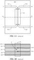
- One type of coupler is a quadrature coupler shown in FIGS. 1A and 1B to include: a pair of strip conductors SC1, SC2 physically separated one from the other by a dielectric board B1 and disposed between a pair of ground plane conductors GP1, GP2 formed on the upper surfaces of a corresponding one of a pair of dielectric boards B2 and B3, respectively, as shown. More particularly, each one of the pair of strip conductors SC1, SC2 has an input port I1, I2, respectively, coupled to a pair of output ports O1, O2, respectively, through an electromagnetic coupling region CR.
- the electromagnetic coupling region CR is a region where a portion of the strip conductors SR1 SR2, in this configuration, vertically overlay one another and are separated by a vertical gap G. It is in this electromagnetic coupling region CR that radio frequency energy passing through the strip conductors SC1, SC2 is coupled between the pair of strip conductors SC1, SC2 by electromagnetically passing through the gap G. It is noted that the opposing ends of strip conductor SC1 are connected to the input port I1 and the output port O1, respectively, while the opposing ends of the strip conductor SC 2 are connected to the input port I2 and the output port O2, respectively as shown.
- one portion of an input signal fed input port I1 passes to output port O1 and another portion of the input signal at input port I1 is coupled by the electromagnetic coupling region CR to both output ports O1 and O2; output port O2 typically being connected to a matched load, not shown.
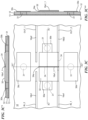
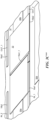
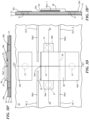
- the above described coupler is sometimes referred to as an overlay coupler; another type of coupler is a broadside coupler ( FIGS. 1C and 1D where instead of the electromagnetic coupling region CR being a pair of overlaying strip conductors, as in FIGS.
- the pair of strip conductors SC1, SC2 are on the same surface of a common dielectric board Ba and the portions of the strip conductors SC1, SC2 in the electromagnetic coupling region CR are in a side by side arrangement and are separated by a horizontal gap G.
- the pair of strip conductors SC1, SC2 are physically separated one from the other by a dielectric boards Ba and B1
- radio frequency energy is electromagnetically coupled between the strip conductors SC1, SC2 by electromagnet energy passing between them through the gap G.
- Couplers Design of Compact Multilevel Folded-Line RF Couplers by Stettaluri et al., IEEE TRANSACTIONS ON MICROWAVE THEORY AND TECHNIQUES, VOL. 47, NO. 12, DECEMBER 1999, pages 2331-2339 ; and COMPACT MULTI-LEVEL FOLDED COUPLED LINE RF COUPLERS, Settaluri et al., 1999 IEEE MTT-S Digest pages 1721-1724 .
- a narrow-band overcoupled directional coupler in multilayer package is known from US5742210 .
- Multilayer microwave couplers using vertically-connected transmission line structures are known from US6208220B1 .
- a multi-layered bi-directional coupler is known from US5576669 .
- an RF coupler as defined by claim 1.
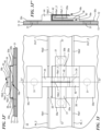
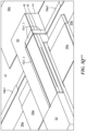
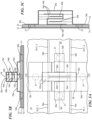
- a structure 10 is shown to include a dielectric substrate 12, having a ground plane conductor 13 on the bottom surface thereof and an RF coupler 14, here for example, a quadrature coupler, formed on an upper surface of the structure 10, at least in part, by additive manufacturing in a manner to be described in connection with FIGS. 3A-3T .
- the structure 10 includes: (A) a pair of strip conductors 16a, 16b, which together with the ground plane conductor 13 and the dielectric substrate 12, provide a pair of microstrip transmission lines 16a, 16b having a pair of input ports IN_1, IN_2, respectively at one end thereof and having output ports OUT_1, OUT_2, respectively, at the opposite ends thereof, as shown; and (B) an RF coupler 14 providing an electromagnetic coupling region 18 for coupling: a portion of an input signal input port IN_1 to output port OUT_1 and another portion of the input signal at input port IN_1 to output port OUT_2; and one portion of an input signal at input port IN_2 to the output port OUT_2 and another portion of the input signal at input port IN_2 to the output port OUT_1.
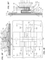
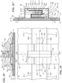
- the electromagnetic coupling region 18 of the RF coupler 18 comprises a plurality of, here for example three, serially connected, vertically stacked, coupling sections 18a, 18b, and 18c; shown more clearly in FIGS. 2B and 2C .
- Each one of the coupling sections 18a, 18b and 18c includes adjacent portions of the pair of strip conductors 16a, 16b, disposed in an overlaying relationship in a vertical plane, and separated by a dielectric gap, G, the gap, G, forming an electromagnetic coupling region between the adjacent portions of the pair of strip conductors.
- the RF coupler 18 includes two, horizontally disposed, electrically conductive layers 20a, 20b, each one of the electrically conductive layers 20a and 20c being disposed between a corresponding pair of the vertically stacked coupling sections 18a, 18b and 18c, as shown. More particularly, conductive layer 20a is disposed between coupling sections 18a and 18b and conductive layer 20b is disposed between coupling sections 18b and 18c.
- An electrically conductive layer 20c and 20d provides an upper or top cover for the RF coupler 14, and electrically conductive layer 20d provides sides for the RF coupler 14; it being noted that the electrically conductive layers 20a-20 are electrically interconnected one to the other and are electrically connected to conductive pads 30a-30; such conductive pads 30a-30d being electrically connected to the ground plane conductor 13 by electrically conductive vias 31 passing vertically through the substrate 12.
- conductive layer 20a provides electromagnetic shielding between the coupling sections 18a and 18b and electrically conductive layer 20b provides electromagnetic shielding between the coupling sections 18b and 18c.
- the RF coupler 14 includes the additional electrically conductive layer 20c is disposed over an upper most one of the serially connected, vertically stacked, coupling sections 18a-18c; here coupling section 18c, as shown to contribute to electromagnetic shielding for the RF coupler.
- Electrically conductive layer 20d is connected to conductive layers 20a-20c to provide an electrically conductive shield on all four sides of the vertically stacked, coupling sections 18a-18c; portions of conductive layers 20c being on opposite sides of one another and portions of layer 20d being on being on opposite sides of one another.
- the plurality of electrically conductive layers, 20a-20d is electrically interconnected to form an electrical shield 22 around the coupling sections 18a-18c.
- various conductive layers 20a-20d and portions of the strip conductors 16a, 16b of the RF coupler 18 are separated (electrically insulated) one from the other by various dielectric layers 32, 38, 40, 42, 44, 46, 48, 50, 52, and 54, to be described below in connection with FIG. 3A-3T .
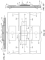
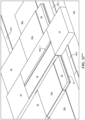
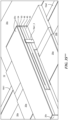
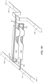
- FIG. 4 is a perspective sketch of portions of the coupler of FIG. 2A with dielectric layers thereof being removed and a portion of one of the electrically conductive layers thereof partially broken away for simplicity in understanding the orientation of other shown portions of the coupler.
- the upper surface of the substrate 12, with the ground plane conductor 13 on the bottom thereof, has a pattern of conductive elements formed thereon for example by etching a sheet of conductive material or by a 3D printing or additive manufacturing, to form: ground plane conductive pads 30a, 30b, 30c and 30d connected to the ground plane conductor 13 ( FIG. 2A ) by electrically conductive vias 31, as indicated; portions 16a 1 of the strip conductors 16a; portions 16a 2 of the strip conductors 16a; portions 16b 1 of the strip conductors 16b; and portions 16b 2 of the strip conductors 16b.
- a dielectric layer 32 is 3D printed over the area of the surface of the substrate 12 where the coupling region 18 is to be formed; a portion of the dielectric layer 32 being disposed on portions 34 of the portions 16b 2 of the strip conductor 16b, as shown; it being noted that an end portion 34a of the portion 16b 2 of the strip conductor 16b remaining uncovered by the dielectric layer 32.
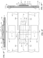
- a conductive strip portions 16a1_1 of strip conductor 16a are printed on a vertical edge of the dielectric layer 32 and up and onto the surface of the dielectric layer 32 to connect conductive strip portions 16a1 to portion 16a1_1; it being noted that conductive strip portions 16a1_1 is printed vertically over the portion 34 of strip conductive 16b2 ( FIG. 3A ) but separated by portions of the dielectric layer 32 ( FIG. 3B ) layer thereby forming the coupling section 18a; it being again noted that end portion 34a of the portion 16b 2 of the strip conductor 16b, remains uncovered by the dielectric layer 32.
- a dielectric layer 38 is 3D printed over the first coupling section 18a leaving an outer edge 16a1_1a of conductive strip portion 16a1_1 exposed; it being remember that end portion 34a of the portions 16b 2 of the strip conductor 16b remain uncovered by the dielectric layer 32.
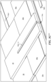
- conductive layer 20a is printed onto the top of dielectric layer 38 and over the sides (vertical edges of) the dielectric layers 32 and 38 onto the pads 30a, 30b, as shown.
- a dielectric layer 40 is printed over portions of the conductive layer 20a on the upper surface while leaving side portions 20a of layer 20a exposed, as shown.
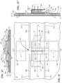
- conductive layer 16a1_2 is printed onto the surface of dielectric layer 40 and over the outer, vertical edges of dielectric layers 38 and 40 and onto edge 16a1_1a to connect the conductive layer 16a1_1 to conductive layer 16a1_2.
- a dielectric layer 42 is printed over the conductive layer 16a1_2 and over the vertical side of such conductive layer 16a1_2, as shown. It is noted that end 16a1_2a of strip 16a1_2 is left exposed as shown.
- a conductive strip 16b2_1 is printed over dielectric 42 and aligned vertically over conductive strip 16a1_2 to form the second coupling section18b; it being noted that such conductive material 16b2_1 is printed over the portions of the dielectric layer both on the upper surface and side of the structure shown in FIG. 3I ′′′ with a portion of the conductive strip 16b2_1 being printed on the edge portion 34a of the portion 34 of strip conductor 16b2 thereby connecting strip conductor 16b2_1 strip conductor 16b2 serially connecting coupling section 18a to coupling section 18b. It is noted that end 16a2_1a of strip conductor 16a2_1 remains exposed by both the strip conductor 16b2_1 and the dielectric layer 42.
- a dielectric layer 44 is printed to fill a space 45 ( FIG. 3I ) on the surface next to previously printed sections of substrate 12, as shown.
- This dielectric layer 44 should be printed to same height of the dielectric layers next to it to form a level dielectric surface for subsequent processing of the coupling region.
- a dielectric layer 46 is printed on the structure shown in FIG. 3J thus formed leaving ends 16a1_2a and 16b2_1a of strip conductors 16a1_2 and 16b2_1 , respectively, exposed, as shown.
- the conductive layer 20b is printed on top of the middle portion of dielectric layer 46, as shown.
- a dielectric layer 48 is printed on the surface of the structure shown in FIG. 3L thus formed over conductive layer 20b, as shown.
- a conductive strip 16b1_2 is printed on the end of strip conductor 16b1, up and along the sides of dielectric layers 44, 46 and 48 along the upper surface of dielectric layer 48 and then down the sides of dielectric layers 48 and 46 to connect with the end 16b2_1a of strip conductor 16b2_1, as shown.
- a dielectric layer 50 is printed on top of the structure shown in FIG. 3N over the portion of strip conductor 16b2_1 on the upper surface of dielectric layer 48 and over the portion of the strip conductor 16b2_1 along the sides of dielectric layers 48 and 46, as shown.
- a conductive strip 16a1_3 is printed on the edge 16a1_2a of strip conductor 16a1_2, along the vertical sides of dielectric layer 50 along the upper, horizontal surface of dielectric layer 50 vertically aligned over the strip conductor 16b2_1 on the surface of dielectric layer 48, forming the third coupling section 18c, and then down the sides of dielectric layers 50, 48, 46 and 44 to connect with the end of strip conductor 16a2 which is on the surface of the substrate 12, as shown.
- a dielectric layer 52 is printed to fill space 51 ( FIG. 3P ) to provide a level surface as across the coupling region being formed, as shown.
- dielectric layer 54 is printed as shown to cover both the horizontal portion and vertical portion of the strip conductor 16a1_3 on the top and vertical sides of the structure shown in FIG. 3Q while exposing strip conductors 16a1, 16b1, 16a2 and 16b2, as shown.
- the conductive layer 20c is printed on the upper surface and vertical sides of the structure as shown in FIG. 3S and onto conductive pads 30c and 30d, as shown.
- a conductive layer 20d is printed on the upper surface of and a pair of opposing sides of the structure shown in FIG. 3S and onto conductive pads 30a and 30b and onto edges of layers 20a, 20b, connecting to conductive pads 30a, 30b, as shown thereby completing shield 22 for the coupler 10.
- the conductive pads 30a-30d may be connected to the ground plane by conductive vias 31, passing through the substrate or by printing a conductor around sides of the substrate between the conductive pads 30a-30d and the ground plane.
- the conductive layers are here printed with any suitable conductive ink and the dielectric layers may be printed with any suitable dielectric ink.
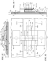
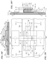
- the electromagnetic coupling region 18' includes a plurality, here for example, three electromagnetic coupling sections 18a'-18c'. More particularly, electromagnetic coupling region 18' comprises a plurality of, here for example three, serially connected, vertically stacked, coupling sections 18a', 18b', and 18c'.
- each one of the coupling sections 18a', 18b' and 18c' includes adjacent portions of the pair of strip conductors 16'a, 16'b, having portions thereof disposed in a side-by-side relationship in a horizontal plane in each of the coupling sections.
- the portions of the strip conductors 16a, 16b in each pair in the coupling sections 18a', 18b' and 18c' are separated by a dielectric gap, G', here the gap G' is disposed in a horizontal, the gap, G', in the forming an electromagnetic coupling region between the adjacent portions of the pair of strip conductors 16a, 16b.
- the RF coupler 10' includes two, horizontally disposed, electrically conductive layers 20a, 20b, each one of the electrically conductive layers 20a and 20c being disposed between a corresponding pair of the vertically stacked coupling sections 18a', 18b' and 18c', as shown. More particularly, conductive layer 20a is disposed between coupling sections 18a' and 18b' and conductive layer 20b is disposed between coupling sections 18b' and 18c'.
- An electrically conductive layer 20c and 20d provides an upper or top cover for the RF coupler 14', and electrically conductive layer 20d provides sides for the RF coupler 14'; it being noted that the electrically conductive layers 20a-20d are electrically interconnected one to the other and are electrically connected to conductive pads 30a-30d; such conductive pads 30a-30d being electrically connected to the ground plane conductor 13 by electrically conductive vias 31 passing vertically through the substrate 12 n connection with hybrid coupler 10, FIG. 2A to provide the electrostatically conductive shield 22 around the coupling sections 18a'-18c' as described in FIG. 2A .
- the strip conductor 16a' includes serially connected conductive layers 16a' 1 through layer 16a'5 and strip conductor 16b' layer 16a' includes serially connected conductive layers 16b'1 through layer 16b'5.
- the coupler 10' is formed by 3D printing or additive manufacture by the following material deposition sequence: Strip conductor layers 16'a1 and 16b' 1; dielectric layer DL1; conductive layer 20a; dielectric layer DL2; strip conductors layers 16'a2, 16b'2 ; strip conductor layers 16a'3, 16b'3 (connecting strip conductors layers 16'a1, 16b'1 to strip conductor layers 16a'2, 16b'2, respectively); dielectric layer DL 3; dielectric layer DL4; conductive layer 20b; dielectric layer DL5; strip conductor layers 16a'4, 16b'4; strip conductor layers 16a'5, 16b'5 (connecting strip conductor layers 16a'4, 16b'4 to strip conductor layers 16a'2, 16b'2, respectively); dielectric layer DL6; dielectric layer DL 7; conductive layer 20c;; and conductive layer 20d (connecting conductive layers 20a, 20b and 20c and also connecting such conductive layers 20a, 20b and 20c to
Landscapes
- Shielding Devices Or Components To Electric Or Magnetic Fields (AREA)
- Waveguide Connection Structure (AREA)
- Waveguides (AREA)
Claims (4)
- Coupleur RF (14) comprenant :
une paire de bandes conductrices diélectriquement séparées (16a, b), la paire de bandes conductrices diélectriquement séparées ayant une région de couplage (18), la région de couplage comprenant :une pluralité de sections de couplage (18a-c) empilées verticalement, connectées en série, chacune des sections de couplage comprenant une partie de la paire de bandes conductrices séparées par un espace diélectrique, l'espace formant une région de couplage électromagnétique entre la partie du paire de bandes conductrices ;une pluralité de couches électriquement conductrices (20a, b), chacune des couches électriquement conductrices étant disposée entre une paire de sections de couplage empilées verticalement ;une couche électriquement conductrice supplémentaire disposée sur la partie supérieure des sections de couplage empilées verticalement connectées en série ; et caractérisé en ce que la couche électriquement conductrice supplémentaire se trouve sur les côtés des sections de couplage empilées verticalement, et dans lequel la pluralité de couches électriquement conductrices et la couche électriquement conductrice supplémentaire sont électriquement interconnectées pour former un blindage électrique autour des sections de couplage. - Coupleur RF selon la revendication 1, dans lequel la paire de bandes conductrices dans chacune des sections de couplage est disposée côte à côte dans un plan horizontal.
- Coupleur RF selon la revendication 1, dans lequel la paire de bandes conductrices dans chacune des sections de couplage est disposée dans une relation verticale superposée.
- Coupleur RF, comprenant :une paire de ports d'entrée ;une paire de ports de sortie ;une région de couplage pour coupler :une partie d'un signal d'entrée transmise à un premier des ports d'entrée vers un premier des ports de sortie et une autre partie du signal d'entrée transmise au premier des ports d'entrée vers un second des ports de sortie ; etune partie d'un signal d'entrée transmise à un second des ports d'entrée vers un second des ports de sortie et une autre partie du signal d'entrée transmise au second des ports d'entrée vers le premier des ports de sortie ;dans lequel la région de couplage comprend le coupleur RF énoncé dans l'une quelconque des revendications 1 à 3.
Applications Claiming Priority (2)
| Application Number | Priority Date | Filing Date | Title |
|---|---|---|---|
| US15/693,743 US10511076B2 (en) | 2017-09-01 | 2017-09-01 | RF coupler including vertically stacked coupling sections having conductive layers disposed between the coupling sections and the coupler including a surrounding electric shield |
| PCT/US2018/043858 WO2019045920A1 (fr) | 2017-09-01 | 2018-07-26 | Coupleur radiofréquence (rf) |
Publications (2)
| Publication Number | Publication Date |
|---|---|
| EP3676907A1 EP3676907A1 (fr) | 2020-07-08 |
| EP3676907B1 true EP3676907B1 (fr) | 2024-07-17 |
Family
ID=63165531
Family Applications (1)
| Application Number | Title | Priority Date | Filing Date |
|---|---|---|---|
| EP18752978.9A Active EP3676907B1 (fr) | 2017-09-01 | 2018-07-26 | Coupleur radiofréquence (rf) |
Country Status (7)
| Country | Link |
|---|---|
| US (1) | US10511076B2 (fr) |
| EP (1) | EP3676907B1 (fr) |
| JP (1) | JP6968986B2 (fr) |
| KR (1) | KR102360415B1 (fr) |
| ES (1) | ES2985793T3 (fr) |
| PL (1) | PL3676907T3 (fr) |
| WO (1) | WO2019045920A1 (fr) |
Families Citing this family (1)
| Publication number | Priority date | Publication date | Assignee | Title |
|---|---|---|---|---|
| US11177547B1 (en) | 2020-05-05 | 2021-11-16 | Raytheon Company | Three-dimensional branch line coupler |
Family Cites Families (6)
| Publication number | Priority date | Publication date | Assignee | Title |
|---|---|---|---|---|
| US3506932A (en) | 1968-02-28 | 1970-04-14 | Bell Telephone Labor Inc | Quadrature hybrid coupler |
| FR2635920B1 (fr) * | 1988-08-30 | 1990-10-12 | Thomson Csf | Procede de fabrication d'une zone de connexion pour un circuit hyperfrequence de type triplaque et circuit ainsi obtenu |
| JP2817487B2 (ja) * | 1991-12-09 | 1998-10-30 | 株式会社村田製作所 | チップ型方向性結合器 |
| US5576669A (en) | 1995-04-28 | 1996-11-19 | Motorola, Inc. | Multi-layered bi-directional coupler |
| US5742210A (en) | 1997-02-12 | 1998-04-21 | Motorola Inc. | Narrow-band overcoupled directional coupler in multilayer package |
| US6208220B1 (en) * | 1999-06-11 | 2001-03-27 | Merrimac Industries, Inc. | Multilayer microwave couplers using vertically-connected transmission line structures |
-
2017
- 2017-09-01 US US15/693,743 patent/US10511076B2/en active Active
-
2018
- 2018-07-26 JP JP2020512407A patent/JP6968986B2/ja active Active
- 2018-07-26 EP EP18752978.9A patent/EP3676907B1/fr active Active
- 2018-07-26 ES ES18752978T patent/ES2985793T3/es active Active
- 2018-07-26 PL PL18752978.9T patent/PL3676907T3/pl unknown
- 2018-07-26 KR KR1020197037339A patent/KR102360415B1/ko active Active
- 2018-07-26 WO PCT/US2018/043858 patent/WO2019045920A1/fr not_active Ceased
Also Published As
| Publication number | Publication date |
|---|---|
| WO2019045920A1 (fr) | 2019-03-07 |
| US10511076B2 (en) | 2019-12-17 |
| KR102360415B1 (ko) | 2022-02-08 |
| JP6968986B2 (ja) | 2021-11-24 |
| JP2020532907A (ja) | 2020-11-12 |
| EP3676907A1 (fr) | 2020-07-08 |
| PL3676907T3 (pl) | 2024-09-23 |
| ES2985793T3 (es) | 2024-11-07 |
| US20190074567A1 (en) | 2019-03-07 |
| KR20200004889A (ko) | 2020-01-14 |
Similar Documents
| Publication | Publication Date | Title |
|---|---|---|
| US6097260A (en) | Distributed ground pads for shielding cross-overs of mutually overlapping stripline signal transmission networks | |
| EP2232641B1 (fr) | Module d'alimentation d'antenne | |
| JP2817487B2 (ja) | チップ型方向性結合器 | |
| US4647878A (en) | Coaxial shielded directional microwave coupler | |
| KR940006510B1 (ko) | 저온 소성 세라믹에 의한 스트립라인 차폐 구조물 | |
| US6765298B2 (en) | Substrate pads with reduced impedance mismatch and methods to fabricate substrate pads | |
| EP0978896B1 (fr) | Ligne de transmission et résonateur du type de ligne de transmission | |
| GB2246922A (en) | Delay line device | |
| EP3828924B1 (fr) | Structure d'interconnexion verticale d'un substrat multicouche | |
| US8106721B2 (en) | Multilayer complementary-conducting-strip transmission line structure with plural interlaced signal lines and mesh ground planes | |
| US6756860B2 (en) | Dual band coupler | |
| IL146912A (en) | Electrical transmission arrangement | |
| JP4198912B2 (ja) | 対称ストリップラインと非対称ストリップラインの間の遷移構造 | |
| US8154364B2 (en) | High-frequency transmission line having ground surface patterns with a plurality of notches therein | |
| KR102040790B1 (ko) | 무선통신용 연성회로기판 | |
| JPS58117701A (ja) | 高周波ストリツプ線路 | |
| KR102360415B1 (ko) | 무선 주파수(rf) 커플러 | |
| US20100301962A1 (en) | Composite balun | |
| KR102428983B1 (ko) | 도파관 | |
| US7525397B2 (en) | Stripline directional coupler having a wide coupling gap | |
| KR102454812B1 (ko) | 다층형 방향성 커플러 | |
| WO2023133750A1 (fr) | Transitions carte à carte à bande ultra-large pour lignes de transmission rf à ligne-ruban | |
| JP4471281B2 (ja) | 積層型高周波回路基板 | |
| KR20050029928A (ko) | 적층형 세라믹 커플러 | |
| EP1198860B1 (fr) | Systeme de transmission electrique |
Legal Events
| Date | Code | Title | Description |
|---|---|---|---|
| STAA | Information on the status of an ep patent application or granted ep patent |
Free format text: STATUS: UNKNOWN |
|
| STAA | Information on the status of an ep patent application or granted ep patent |
Free format text: STATUS: THE INTERNATIONAL PUBLICATION HAS BEEN MADE |
|
| PUAI | Public reference made under article 153(3) epc to a published international application that has entered the european phase |
Free format text: ORIGINAL CODE: 0009012 |
|
| STAA | Information on the status of an ep patent application or granted ep patent |
Free format text: STATUS: REQUEST FOR EXAMINATION WAS MADE |
|
| 17P | Request for examination filed |
Effective date: 20200107 |
|
| AK | Designated contracting states |
Kind code of ref document: A1 Designated state(s): AL AT BE BG CH CY CZ DE DK EE ES FI FR GB GR HR HU IE IS IT LI LT LU LV MC MK MT NL NO PL PT RO RS SE SI SK SM TR |
|
| AX | Request for extension of the european patent |
Extension state: BA ME |
|
| DAV | Request for validation of the european patent (deleted) | ||
| DAX | Request for extension of the european patent (deleted) | ||
| STAA | Information on the status of an ep patent application or granted ep patent |
Free format text: STATUS: EXAMINATION IS IN PROGRESS |
|
| 17Q | First examination report despatched |
Effective date: 20220218 |
|
| GRAP | Despatch of communication of intention to grant a patent |
Free format text: ORIGINAL CODE: EPIDOSNIGR1 |
|
| STAA | Information on the status of an ep patent application or granted ep patent |
Free format text: STATUS: GRANT OF PATENT IS INTENDED |
|
| INTG | Intention to grant announced |
Effective date: 20240108 |
|
| GRAJ | Information related to disapproval of communication of intention to grant by the applicant or resumption of examination proceedings by the epo deleted |
Free format text: ORIGINAL CODE: EPIDOSDIGR1 |
|
| STAA | Information on the status of an ep patent application or granted ep patent |
Free format text: STATUS: EXAMINATION IS IN PROGRESS |
|
| GRAP | Despatch of communication of intention to grant a patent |
Free format text: ORIGINAL CODE: EPIDOSNIGR1 |
|
| STAA | Information on the status of an ep patent application or granted ep patent |
Free format text: STATUS: GRANT OF PATENT IS INTENDED |
|
| INTC | Intention to grant announced (deleted) | ||
| GRAS | Grant fee paid |
Free format text: ORIGINAL CODE: EPIDOSNIGR3 |
|
| GRAA | (expected) grant |
Free format text: ORIGINAL CODE: 0009210 |
|
| STAA | Information on the status of an ep patent application or granted ep patent |
Free format text: STATUS: THE PATENT HAS BEEN GRANTED |
|
| INTG | Intention to grant announced |
Effective date: 20240522 |
|
| AK | Designated contracting states |
Kind code of ref document: B1 Designated state(s): AL AT BE BG CH CY CZ DE DK EE ES FI FR GB GR HR HU IE IS IT LI LT LU LV MC MK MT NL NO PL PT RO RS SE SI SK SM TR |
|
| REG | Reference to a national code |
Ref country code: CH Ref legal event code: EP |
|
| REG | Reference to a national code |
Ref country code: DE Ref legal event code: R096 Ref document number: 602018071864 Country of ref document: DE |
|
| REG | Reference to a national code |
Ref country code: IE Ref legal event code: FG4D |
|
| REG | Reference to a national code |
Ref country code: ES Ref legal event code: FG2A Ref document number: 2985793 Country of ref document: ES Kind code of ref document: T3 Effective date: 20241107 |
|
| REG | Reference to a national code |
Ref country code: LT Ref legal event code: MG9D |
|
| REG | Reference to a national code |
Ref country code: NL Ref legal event code: MP Effective date: 20240717 |
|
| PG25 | Lapsed in a contracting state [announced via postgrant information from national office to epo] |
Ref country code: PT Free format text: LAPSE BECAUSE OF FAILURE TO SUBMIT A TRANSLATION OF THE DESCRIPTION OR TO PAY THE FEE WITHIN THE PRESCRIBED TIME-LIMIT Effective date: 20241118 |
|
| REG | Reference to a national code |
Ref country code: AT Ref legal event code: MK05 Ref document number: 1705017 Country of ref document: AT Kind code of ref document: T Effective date: 20240717 |
|
| PG25 | Lapsed in a contracting state [announced via postgrant information from national office to epo] |
Ref country code: NL Free format text: LAPSE BECAUSE OF FAILURE TO SUBMIT A TRANSLATION OF THE DESCRIPTION OR TO PAY THE FEE WITHIN THE PRESCRIBED TIME-LIMIT Effective date: 20240717 |
|
| PG25 | Lapsed in a contracting state [announced via postgrant information from national office to epo] |
Ref country code: PT Free format text: LAPSE BECAUSE OF FAILURE TO SUBMIT A TRANSLATION OF THE DESCRIPTION OR TO PAY THE FEE WITHIN THE PRESCRIBED TIME-LIMIT Effective date: 20241118 Ref country code: NL Free format text: LAPSE BECAUSE OF FAILURE TO SUBMIT A TRANSLATION OF THE DESCRIPTION OR TO PAY THE FEE WITHIN THE PRESCRIBED TIME-LIMIT Effective date: 20240717 |
|
| PG25 | Lapsed in a contracting state [announced via postgrant information from national office to epo] |
Ref country code: NO Free format text: LAPSE BECAUSE OF FAILURE TO SUBMIT A TRANSLATION OF THE DESCRIPTION OR TO PAY THE FEE WITHIN THE PRESCRIBED TIME-LIMIT Effective date: 20241017 |
|
| PG25 | Lapsed in a contracting state [announced via postgrant information from national office to epo] |
Ref country code: GR Free format text: LAPSE BECAUSE OF FAILURE TO SUBMIT A TRANSLATION OF THE DESCRIPTION OR TO PAY THE FEE WITHIN THE PRESCRIBED TIME-LIMIT Effective date: 20241018 Ref country code: FI Free format text: LAPSE BECAUSE OF FAILURE TO SUBMIT A TRANSLATION OF THE DESCRIPTION OR TO PAY THE FEE WITHIN THE PRESCRIBED TIME-LIMIT Effective date: 20240717 |
|
| PG25 | Lapsed in a contracting state [announced via postgrant information from national office to epo] |
Ref country code: BG Free format text: LAPSE BECAUSE OF FAILURE TO SUBMIT A TRANSLATION OF THE DESCRIPTION OR TO PAY THE FEE WITHIN THE PRESCRIBED TIME-LIMIT Effective date: 20240717 |
|
| PG25 | Lapsed in a contracting state [announced via postgrant information from national office to epo] |
Ref country code: LV Free format text: LAPSE BECAUSE OF FAILURE TO SUBMIT A TRANSLATION OF THE DESCRIPTION OR TO PAY THE FEE WITHIN THE PRESCRIBED TIME-LIMIT Effective date: 20240717 |
|
| PG25 | Lapsed in a contracting state [announced via postgrant information from national office to epo] |
Ref country code: IS Free format text: LAPSE BECAUSE OF FAILURE TO SUBMIT A TRANSLATION OF THE DESCRIPTION OR TO PAY THE FEE WITHIN THE PRESCRIBED TIME-LIMIT Effective date: 20241117 Ref country code: AT Free format text: LAPSE BECAUSE OF FAILURE TO SUBMIT A TRANSLATION OF THE DESCRIPTION OR TO PAY THE FEE WITHIN THE PRESCRIBED TIME-LIMIT Effective date: 20240717 |
|
| PG25 | Lapsed in a contracting state [announced via postgrant information from national office to epo] |
Ref country code: HR Free format text: LAPSE BECAUSE OF FAILURE TO SUBMIT A TRANSLATION OF THE DESCRIPTION OR TO PAY THE FEE WITHIN THE PRESCRIBED TIME-LIMIT Effective date: 20240717 |
|
| PG25 | Lapsed in a contracting state [announced via postgrant information from national office to epo] |
Ref country code: RS Free format text: LAPSE BECAUSE OF FAILURE TO SUBMIT A TRANSLATION OF THE DESCRIPTION OR TO PAY THE FEE WITHIN THE PRESCRIBED TIME-LIMIT Effective date: 20241017 |
|
| PG25 | Lapsed in a contracting state [announced via postgrant information from national office to epo] |
Ref country code: RS Free format text: LAPSE BECAUSE OF FAILURE TO SUBMIT A TRANSLATION OF THE DESCRIPTION OR TO PAY THE FEE WITHIN THE PRESCRIBED TIME-LIMIT Effective date: 20241017 Ref country code: NO Free format text: LAPSE BECAUSE OF FAILURE TO SUBMIT A TRANSLATION OF THE DESCRIPTION OR TO PAY THE FEE WITHIN THE PRESCRIBED TIME-LIMIT Effective date: 20241017 Ref country code: LV Free format text: LAPSE BECAUSE OF FAILURE TO SUBMIT A TRANSLATION OF THE DESCRIPTION OR TO PAY THE FEE WITHIN THE PRESCRIBED TIME-LIMIT Effective date: 20240717 Ref country code: IS Free format text: LAPSE BECAUSE OF FAILURE TO SUBMIT A TRANSLATION OF THE DESCRIPTION OR TO PAY THE FEE WITHIN THE PRESCRIBED TIME-LIMIT Effective date: 20241117 Ref country code: HR Free format text: LAPSE BECAUSE OF FAILURE TO SUBMIT A TRANSLATION OF THE DESCRIPTION OR TO PAY THE FEE WITHIN THE PRESCRIBED TIME-LIMIT Effective date: 20240717 Ref country code: GR Free format text: LAPSE BECAUSE OF FAILURE TO SUBMIT A TRANSLATION OF THE DESCRIPTION OR TO PAY THE FEE WITHIN THE PRESCRIBED TIME-LIMIT Effective date: 20241018 Ref country code: FI Free format text: LAPSE BECAUSE OF FAILURE TO SUBMIT A TRANSLATION OF THE DESCRIPTION OR TO PAY THE FEE WITHIN THE PRESCRIBED TIME-LIMIT Effective date: 20240717 Ref country code: BG Free format text: LAPSE BECAUSE OF FAILURE TO SUBMIT A TRANSLATION OF THE DESCRIPTION OR TO PAY THE FEE WITHIN THE PRESCRIBED TIME-LIMIT Effective date: 20240717 Ref country code: AT Free format text: LAPSE BECAUSE OF FAILURE TO SUBMIT A TRANSLATION OF THE DESCRIPTION OR TO PAY THE FEE WITHIN THE PRESCRIBED TIME-LIMIT Effective date: 20240717 |
|
| REG | Reference to a national code |
Ref country code: CH Ref legal event code: PL |
|
| PG25 | Lapsed in a contracting state [announced via postgrant information from national office to epo] |
Ref country code: LU Free format text: LAPSE BECAUSE OF NON-PAYMENT OF DUE FEES Effective date: 20240726 |
|
| PG25 | Lapsed in a contracting state [announced via postgrant information from national office to epo] |
Ref country code: LU Free format text: LAPSE BECAUSE OF NON-PAYMENT OF DUE FEES Effective date: 20240726 |
|
| PG25 | Lapsed in a contracting state [announced via postgrant information from national office to epo] |
Ref country code: DK Free format text: LAPSE BECAUSE OF FAILURE TO SUBMIT A TRANSLATION OF THE DESCRIPTION OR TO PAY THE FEE WITHIN THE PRESCRIBED TIME-LIMIT Effective date: 20240717 Ref country code: RO Free format text: LAPSE BECAUSE OF FAILURE TO SUBMIT A TRANSLATION OF THE DESCRIPTION OR TO PAY THE FEE WITHIN THE PRESCRIBED TIME-LIMIT Effective date: 20240717 Ref country code: SM Free format text: LAPSE BECAUSE OF FAILURE TO SUBMIT A TRANSLATION OF THE DESCRIPTION OR TO PAY THE FEE WITHIN THE PRESCRIBED TIME-LIMIT Effective date: 20240717 |
|
| REG | Reference to a national code |
Ref country code: DE Ref legal event code: R097 Ref document number: 602018071864 Country of ref document: DE |
|
| PG25 | Lapsed in a contracting state [announced via postgrant information from national office to epo] |
Ref country code: BE Free format text: LAPSE BECAUSE OF NON-PAYMENT OF DUE FEES Effective date: 20240731 Ref country code: MC Free format text: LAPSE BECAUSE OF FAILURE TO SUBMIT A TRANSLATION OF THE DESCRIPTION OR TO PAY THE FEE WITHIN THE PRESCRIBED TIME-LIMIT Effective date: 20240717 Ref country code: CH Free format text: LAPSE BECAUSE OF NON-PAYMENT OF DUE FEES Effective date: 20240731 Ref country code: EE Free format text: LAPSE BECAUSE OF FAILURE TO SUBMIT A TRANSLATION OF THE DESCRIPTION OR TO PAY THE FEE WITHIN THE PRESCRIBED TIME-LIMIT Effective date: 20240717 |
|
| PG25 | Lapsed in a contracting state [announced via postgrant information from national office to epo] |
Ref country code: CZ Free format text: LAPSE BECAUSE OF FAILURE TO SUBMIT A TRANSLATION OF THE DESCRIPTION OR TO PAY THE FEE WITHIN THE PRESCRIBED TIME-LIMIT Effective date: 20240717 |
|
| PG25 | Lapsed in a contracting state [announced via postgrant information from national office to epo] |
Ref country code: SK Free format text: LAPSE BECAUSE OF FAILURE TO SUBMIT A TRANSLATION OF THE DESCRIPTION OR TO PAY THE FEE WITHIN THE PRESCRIBED TIME-LIMIT Effective date: 20240717 |
|
| PLBE | No opposition filed within time limit |
Free format text: ORIGINAL CODE: 0009261 |
|
| STAA | Information on the status of an ep patent application or granted ep patent |
Free format text: STATUS: NO OPPOSITION FILED WITHIN TIME LIMIT |
|
| REG | Reference to a national code |
Ref country code: BE Ref legal event code: MM Effective date: 20240731 |
|
| 26N | No opposition filed |
Effective date: 20250422 |
|
| PGFP | Annual fee paid to national office [announced via postgrant information from national office to epo] |
Ref country code: PL Payment date: 20250625 Year of fee payment: 8 |
|
| PGFP | Annual fee paid to national office [announced via postgrant information from national office to epo] |
Ref country code: GB Payment date: 20250619 Year of fee payment: 8 |
|
| PGFP | Annual fee paid to national office [announced via postgrant information from national office to epo] |
Ref country code: FR Payment date: 20250620 Year of fee payment: 8 |
|
| PG25 | Lapsed in a contracting state [announced via postgrant information from national office to epo] |
Ref country code: IE Free format text: LAPSE BECAUSE OF NON-PAYMENT OF DUE FEES Effective date: 20240726 |
|
| PG25 | Lapsed in a contracting state [announced via postgrant information from national office to epo] |
Ref country code: SE Free format text: LAPSE BECAUSE OF FAILURE TO SUBMIT A TRANSLATION OF THE DESCRIPTION OR TO PAY THE FEE WITHIN THE PRESCRIBED TIME-LIMIT Effective date: 20240717 |
|
| PGFP | Annual fee paid to national office [announced via postgrant information from national office to epo] |
Ref country code: ES Payment date: 20250801 Year of fee payment: 8 |
|
| PGFP | Annual fee paid to national office [announced via postgrant information from national office to epo] |
Ref country code: DE Payment date: 20250620 Year of fee payment: 8 |
|
| PG25 | Lapsed in a contracting state [announced via postgrant information from national office to epo] |
Ref country code: IT Free format text: LAPSE BECAUSE OF NON-PAYMENT OF DUE FEES Effective date: 20240726 |
|
| PG25 | Lapsed in a contracting state [announced via postgrant information from national office to epo] |
Ref country code: CY Free format text: LAPSE BECAUSE OF FAILURE TO SUBMIT A TRANSLATION OF THE DESCRIPTION OR TO PAY THE FEE WITHIN THE PRESCRIBED TIME-LIMIT; INVALID AB INITIO Effective date: 20180726 |
|
| PG25 | Lapsed in a contracting state [announced via postgrant information from national office to epo] |
Ref country code: HU Free format text: LAPSE BECAUSE OF FAILURE TO SUBMIT A TRANSLATION OF THE DESCRIPTION OR TO PAY THE FEE WITHIN THE PRESCRIBED TIME-LIMIT; INVALID AB INITIO Effective date: 20180726 |
|
| PG25 | Lapsed in a contracting state [announced via postgrant information from national office to epo] |
Ref country code: IT Free format text: LAPSE BECAUSE OF NON-PAYMENT OF DUE FEES Effective date: 20240726 |
|
| PGFP | Annual fee paid to national office [announced via postgrant information from national office to epo] |
Ref country code: IT Payment date: 20250619 Year of fee payment: 8 |
|
| PGRI | Patent reinstated in contracting state [announced from national office to epo] |
Ref country code: IT Effective date: 20241202 |