EP3677606B1 - Polymère, composition de revêtement le comprenant, et dispositif électroluminescent organique l'utilisant - Google Patents
Polymère, composition de revêtement le comprenant, et dispositif électroluminescent organique l'utilisant Download PDFInfo
- Publication number
- EP3677606B1 EP3677606B1 EP19743508.4A EP19743508A EP3677606B1 EP 3677606 B1 EP3677606 B1 EP 3677606B1 EP 19743508 A EP19743508 A EP 19743508A EP 3677606 B1 EP3677606 B1 EP 3677606B1
- Authority
- EP
- European Patent Office
- Prior art keywords
- group
- substituted
- unsubstituted
- polymer
- light emitting
- Prior art date
- Legal status (The legal status is an assumption and is not a legal conclusion. Google has not performed a legal analysis and makes no representation as to the accuracy of the status listed.)
- Active
Links
Images


Classifications
-
- C—CHEMISTRY; METALLURGY
- C08—ORGANIC MACROMOLECULAR COMPOUNDS; THEIR PREPARATION OR CHEMICAL WORKING-UP; COMPOSITIONS BASED THEREON
- C08F—MACROMOLECULAR COMPOUNDS OBTAINED BY REACTIONS ONLY INVOLVING CARBON-TO-CARBON UNSATURATED BONDS
- C08F212/00—Copolymers of compounds having one or more unsaturated aliphatic radicals, each having only one carbon-to-carbon double bond, and at least one being terminated by an aromatic carbocyclic ring
- C08F212/02—Monomers containing only one unsaturated aliphatic radical
- C08F212/32—Monomers containing only one unsaturated aliphatic radical containing two or more rings
-
- C—CHEMISTRY; METALLURGY
- C08—ORGANIC MACROMOLECULAR COMPOUNDS; THEIR PREPARATION OR CHEMICAL WORKING-UP; COMPOSITIONS BASED THEREON
- C08F—MACROMOLECULAR COMPOUNDS OBTAINED BY REACTIONS ONLY INVOLVING CARBON-TO-CARBON UNSATURATED BONDS
- C08F212/00—Copolymers of compounds having one or more unsaturated aliphatic radicals, each having only one carbon-to-carbon double bond, and at least one being terminated by an aromatic carbocyclic ring
- C08F212/02—Monomers containing only one unsaturated aliphatic radical
- C08F212/04—Monomers containing only one unsaturated aliphatic radical containing one ring
- C08F212/14—Monomers containing only one unsaturated aliphatic radical containing one ring substituted by heteroatoms or groups containing heteroatoms
- C08F212/22—Oxygen
-
- C—CHEMISTRY; METALLURGY
- C08—ORGANIC MACROMOLECULAR COMPOUNDS; THEIR PREPARATION OR CHEMICAL WORKING-UP; COMPOSITIONS BASED THEREON
- C08F—MACROMOLECULAR COMPOUNDS OBTAINED BY REACTIONS ONLY INVOLVING CARBON-TO-CARBON UNSATURATED BONDS
- C08F212/00—Copolymers of compounds having one or more unsaturated aliphatic radicals, each having only one carbon-to-carbon double bond, and at least one being terminated by an aromatic carbocyclic ring
- C08F212/02—Monomers containing only one unsaturated aliphatic radical
- C08F212/04—Monomers containing only one unsaturated aliphatic radical containing one ring
- C08F212/14—Monomers containing only one unsaturated aliphatic radical containing one ring substituted by heteroatoms or groups containing heteroatoms
- C08F212/22—Oxygen
- C08F212/24—Phenols or alcohols
-
- C—CHEMISTRY; METALLURGY
- C08—ORGANIC MACROMOLECULAR COMPOUNDS; THEIR PREPARATION OR CHEMICAL WORKING-UP; COMPOSITIONS BASED THEREON
- C08F—MACROMOLECULAR COMPOUNDS OBTAINED BY REACTIONS ONLY INVOLVING CARBON-TO-CARBON UNSATURATED BONDS
- C08F212/00—Copolymers of compounds having one or more unsaturated aliphatic radicals, each having only one carbon-to-carbon double bond, and at least one being terminated by an aromatic carbocyclic ring
- C08F212/02—Monomers containing only one unsaturated aliphatic radical
- C08F212/04—Monomers containing only one unsaturated aliphatic radical containing one ring
- C08F212/14—Monomers containing only one unsaturated aliphatic radical containing one ring substituted by heteroatoms or groups containing heteroatoms
- C08F212/26—Nitrogen
-
- C—CHEMISTRY; METALLURGY
- C09—DYES; PAINTS; POLISHES; NATURAL RESINS; ADHESIVES; COMPOSITIONS NOT OTHERWISE PROVIDED FOR; APPLICATIONS OF MATERIALS NOT OTHERWISE PROVIDED FOR
- C09D—COATING COMPOSITIONS, e.g. PAINTS, VARNISHES OR LACQUERS; FILLING PASTES; CHEMICAL PAINT OR INK REMOVERS; INKS; CORRECTING FLUIDS; WOODSTAINS; PASTES OR SOLIDS FOR COLOURING OR PRINTING; USE OF MATERIALS THEREFOR
- C09D125/00—Coating compositions based on homopolymers or copolymers of compounds having one or more unsaturated aliphatic radicals, each having only one carbon-to-carbon double bond, and at least one being terminated by an aromatic carbocyclic ring; Coating compositions based on derivatives of such polymers
- C09D125/18—Homopolymers or copolymers of aromatic monomers containing elements other than carbon and hydrogen
-
- C—CHEMISTRY; METALLURGY
- C09—DYES; PAINTS; POLISHES; NATURAL RESINS; ADHESIVES; COMPOSITIONS NOT OTHERWISE PROVIDED FOR; APPLICATIONS OF MATERIALS NOT OTHERWISE PROVIDED FOR
- C09K—MATERIALS FOR MISCELLANEOUS APPLICATIONS, NOT PROVIDED FOR ELSEWHERE
- C09K11/00—Luminescent materials, e.g. electroluminescent or chemiluminescent
- C09K11/06—Luminescent materials, e.g. electroluminescent or chemiluminescent containing organic luminescent materials
-
- H—ELECTRICITY
- H10—SEMICONDUCTOR DEVICES; ELECTRIC SOLID-STATE DEVICES NOT OTHERWISE PROVIDED FOR
- H10K—ORGANIC ELECTRIC SOLID-STATE DEVICES
- H10K85/00—Organic materials used in the body or electrodes of devices covered by this subclass
- H10K85/10—Organic polymers or oligomers
- H10K85/111—Organic polymers or oligomers comprising aromatic, heteroaromatic, or aryl chains, e.g. polyaniline, polyphenylene or polyphenylene vinylene
- H10K85/115—Polyfluorene; Derivatives thereof
-
- H—ELECTRICITY
- H10—SEMICONDUCTOR DEVICES; ELECTRIC SOLID-STATE DEVICES NOT OTHERWISE PROVIDED FOR
- H10K—ORGANIC ELECTRIC SOLID-STATE DEVICES
- H10K85/00—Organic materials used in the body or electrodes of devices covered by this subclass
- H10K85/10—Organic polymers or oligomers
- H10K85/141—Organic polymers or oligomers comprising aliphatic or olefinic chains, e.g. poly N-vinylcarbazol, PVC or PTFE
-
- H—ELECTRICITY
- H10—SEMICONDUCTOR DEVICES; ELECTRIC SOLID-STATE DEVICES NOT OTHERWISE PROVIDED FOR
- H10K—ORGANIC ELECTRIC SOLID-STATE DEVICES
- H10K85/00—Organic materials used in the body or electrodes of devices covered by this subclass
- H10K85/10—Organic polymers or oligomers
- H10K85/151—Copolymers
-
- C—CHEMISTRY; METALLURGY
- C09—DYES; PAINTS; POLISHES; NATURAL RESINS; ADHESIVES; COMPOSITIONS NOT OTHERWISE PROVIDED FOR; APPLICATIONS OF MATERIALS NOT OTHERWISE PROVIDED FOR
- C09K—MATERIALS FOR MISCELLANEOUS APPLICATIONS, NOT PROVIDED FOR ELSEWHERE
- C09K2211/00—Chemical nature of organic luminescent or tenebrescent compounds
- C09K2211/14—Macromolecular compounds
- C09K2211/1408—Carbocyclic compounds
- C09K2211/1433—Carbocyclic compounds bridged by heteroatoms, e.g. N, P, Si or B
-
- H—ELECTRICITY
- H10—SEMICONDUCTOR DEVICES; ELECTRIC SOLID-STATE DEVICES NOT OTHERWISE PROVIDED FOR
- H10K—ORGANIC ELECTRIC SOLID-STATE DEVICES
- H10K50/00—Organic light-emitting devices
- H10K50/10—OLEDs or polymer light-emitting diodes [PLED]
- H10K50/14—Carrier transporting layers
- H10K50/15—Hole transporting layers
-
- H—ELECTRICITY
- H10—SEMICONDUCTOR DEVICES; ELECTRIC SOLID-STATE DEVICES NOT OTHERWISE PROVIDED FOR
- H10K—ORGANIC ELECTRIC SOLID-STATE DEVICES
- H10K50/00—Organic light-emitting devices
- H10K50/10—OLEDs or polymer light-emitting diodes [PLED]
- H10K50/14—Carrier transporting layers
- H10K50/15—Hole transporting layers
- H10K50/155—Hole transporting layers comprising dopants
-
- H—ELECTRICITY
- H10—SEMICONDUCTOR DEVICES; ELECTRIC SOLID-STATE DEVICES NOT OTHERWISE PROVIDED FOR
- H10K—ORGANIC ELECTRIC SOLID-STATE DEVICES
- H10K50/00—Organic light-emitting devices
- H10K50/10—OLEDs or polymer light-emitting diodes [PLED]
- H10K50/17—Carrier injection layers
-
- H—ELECTRICITY
- H10—SEMICONDUCTOR DEVICES; ELECTRIC SOLID-STATE DEVICES NOT OTHERWISE PROVIDED FOR
- H10K—ORGANIC ELECTRIC SOLID-STATE DEVICES
- H10K50/00—Organic light-emitting devices
- H10K50/10—OLEDs or polymer light-emitting diodes [PLED]
- H10K50/17—Carrier injection layers
- H10K50/171—Electron injection layers
-
- H—ELECTRICITY
- H10—SEMICONDUCTOR DEVICES; ELECTRIC SOLID-STATE DEVICES NOT OTHERWISE PROVIDED FOR
- H10K—ORGANIC ELECTRIC SOLID-STATE DEVICES
- H10K85/00—Organic materials used in the body or electrodes of devices covered by this subclass
- H10K85/60—Organic compounds having low molecular weight
- H10K85/631—Amine compounds having at least two aryl rest on at least one amine-nitrogen atom, e.g. triphenylamine
Definitions
- the present specification relates to a polymer, a coating composition including the polymer, and an organic light emitting device formed using the same.
- An organic light emission phenomenon is one of examples converting a current to visible light by an internal process of specific organic molecules.
- a principle of an organic light emission phenomenon is as follows. When an organic material layer is placed between an anode and a cathode and a current is applied between the two electrodes, electrons and holes are injected to the organic material layer from the cathode and the anode, respectively. The holes and the electrons injected to the organic material layer recombine to form excitons, and light emits when these excitons fall back to the ground state.
- An organic light emitting device using such a principle may be generally formed with a cathode, an anode, and an organic material layer placed therebetween, for example, an organic material layer including a hole injection layer, a hole transfer layer, a light emitting layer and an electron transfer layer.
- Materials used in an organic light emitting device are mostly pure organic materials or complex compounds in which organic materials and metals form complexes, and may be divided into hole injection materials, hole transfer materials, light emitting materials, electron transfer materials, electron injection materials and the like depending on the application.
- organic materials having a p-type property that is, organic materials readily oxidized and having an electrochemically stable state when oxidized
- organic materials having an n-type property that is, organic materials readily reduced and having an electrochemically stable state when reduced, are generally used.
- materials having both a p-type property and an n-type property that is, materials having a stable form in both oxidized and reduced states, are preferred, and materials having high light emission efficiency converting, when excitons are formed, the excitons to light are preferred.
- materials used in an organic light emitting device additionally have properties as follows.
- materials used in an organic light emitting device preferably have excellent thermal stability. This is due to joule heat produced by charge migration in the organic light emitting device.
- N,N'-di(1-naphthyl)-N,N'-diphenyl-(1,1'-biphenyl)-4,4'-diamine (NPB) normally used as a hole transfer layer material currently has a glass transition temperature of 100°C or lower, and has a problem in that it is difficult to use in organic light emitting devices requiring a high current.
- Poly(3,4-ethylenedioxythiophene):poly(styrenesulfonate) (PEDOT:PSS) currently used as a hole transfer material in an organic light emitting device manufactured using a solution coating method has a lower LUMO energy level compared to a LUMO energy level of organic materials used as a light emitting layer material, and therefore, has a problem in manufacturing an organic light emitting device with high efficiency and long lifetime.
- materials used in an organic light emitting device need to have excellent chemical stability, charge mobility, and interface property with electrodes or adjacent layers.
- materials used in an organic light emitting device need to undergo less material deformation caused by moisture or oxygen.
- the materials need to maximize exciton formation through balancing hole and electron density in a light emitting layer of the organic light emitting device.
- the materials also need to improve an interface with electrodes including metals or metal oxides.
- materials used in an organic light emitting device for a solution process additionally need to have properties as follows.
- a storable homogeneous solution needs to be formed.
- Commercialized materials for a deposition process have favorable crystallinity, and are not well-dissolved in a solution, or crystals are readily caught when forming a solution. Therefore, a concentration gradient of the solution may change depending on the storage time or possibility of forming a defective device is high.
- layers going through a solution process need to have solvent and material tolerance for other layers.
- materials capable of forming a self-crosslinked polymer on a substrate through heat treatment or ultraviolet (UV) irradiation after introducing a curing group and solution coating such as N4,N4'-di(naphthalen-1-yl)-N4,N4'-bis(4-vinylphenyl)biphenyl-4,4'-diamine (VNPB) or forming a polymer having sufficient tolerance for a next process are preferred, and materials capable of having solvent tolerance by itself such as hexaazatriphenylene hexacarbonitrile (HATCN) are also preferred.
- UV ultraviolet
- Arylamine-based monomers generally used in an organic light emitting device (OLED) do not have tolerance for a solvent of a next process by themselves, and therefore, arylamine-based monomer compounds usable in an OLED device for a solution process need to have a curing group introduced thereto.
- the present specification is directed to providing a polymer usable in an organic light emitting device for a solution process, a coating composition including the same, and an organic light emitting device formed using the same.
- One embodiment of the present specification provides a polymer including a unit represented by the following Chemical Formula 1; and a unit represented by the following Chemical Formula 2.
- Chemical Formulae 1 and 2 are examples of Chemical Formulae 1 and 2
- Another embodiment of the present specification provides a coating composition including the polymer described above.
- Still another embodiment of the present specification provides an organic light emitting device including a first electrode; a second electrode provided opposite to the first electrode; and one or more organic material layers provided between the first electrode and the second electrode, wherein one or more layers of the organic material layers include a cured material of the coating composition described above.
- a polymer according to one embodiment of the present specification includes a functional group polymerized by heat or light, and when providing sufficient heat or light after forming a film, tolerance for a solvent for a process is developed, and the compound according to one embodiment of the present specification is not washed away or film properties are not changed, and a reproducible organic light emitting device can be manufactured.
- An aryl group (Ar1) directly attached to number 9 carbon of fluorene and a proper spacer between a curing group and the fluorene are capable of controlling a glass transition temperature, a melting point and solubility by inhibiting interactions between molecules, and therefore, this derivative can be used as a material of an organic material layer of an organic light emitting device, and is capable of providing low driving voltage, high light emission efficiency and long lifetime properties.
- this derivative can be used as a material of an organic material layer of an organic light emitting device, and is capable of providing low driving voltage, high light emission efficiency and long lifetime properties.
- solubility increases leading to advantages of widening a range of solvent selection when manufacturing an ink of a solution process, and lowering a melting point and a curing temperature.
- a description of a certain member being placed "on" another member includes not only a case of the one member adjoining the another member but a case of still another member being present between the two members.
- the term "combination thereof" included in a Markush-type expression means a mixture or a combination of one or more selected from the group consisting of constituents described in the Markush-type expression, and means including one or more selected from the group consisting of the constituents.
- One embodiment of the present specification provides a polymer including a unit represented by Chemical Formula 1 and a unit represented by Chemical Formula 2.
- the unit represented by Chemical Formula 1 is a unit derived from a compound in which an amine group bonds to both side benzene rings of the fluorene, and a vinyl group bonds to the number 9 position.
- Y of Chemical Formula 1 represents a long branch-type linker, and in this case, excellent solubility for an organic solvent is obtained.
- the unit represented by Chemical Formula 1 is a unit in which the compound at the number 9 position of the fluorene is asymmetric, and compared to a symmetric unit, is capable of reducing a problem of crystal precipitation during a solution process by reducing interactions between molecules, and is effective in preparing various derivatives.
- the polymer according to one embodiment of the present specification has the main chain and the arylamine part separated due to vinyl condensation, and therefore, performance of a reproducible device may be identified. Since a polymer that does not go through vinyl condensation and has an arylamine group as the main chain is a completely conjugated polymer, electron or hole flow may be too high or balanced charge transfer may not be suitable. In addition, the content of the arylamine in the main chain varies depending on the polymer length, and therefore, the molecular weight may not be reproducibly controlled causing a problem of significantly changing device performance.
- the unit represented by Chemical Formula 2 is a unit derived from a compound having a curing group and a vinyl group.
- a polymer that does not include an additional curing group like Chemical Formula 2 may not exhibit sufficient solvent tolerance, however, the polymer of the present disclosure may form crosslinkage through heat treatment due to the additional curing group included in Chemical Formula 2, and is effective in exhibiting sufficient solvent tolerance.
- a "curing group” may mean a reactive substituent crosslinking compounds by being exposed to heat and/or light.
- the crosslinkage may be produced while linking radicals produced by decomposing carbon-carbon multiple bonds or cyclic structures through heat treatment or light irradiation.
- the curing group is any one of the following structures.
- R10 to R13 are the same as or different from each other and each independently hydrogen, or a substituted or unsubstituted alkyl group, and a wave mark means a site bonding to L3.
- substitution in the present specification means a hydrogen atom bonding to a carbon atom of a compound is changed to another substituent.
- the position of substitution is not limited as long as it is a position at which the hydrogen atom is substituted, that is, a position at which a substituent can substitute, and when two or more substituents substitute, the two or more substituents may be the same as or different from each other.
- substituted or unsubstituted in the present specification means being substituted with one or more substituents selected from the group consisting of hydrogen; deuterium; a halogen group; an alkyl group; a cycloalkyl group; an alkoxy group; an aryl group; an amine group; and an arylamine group or being unsubstituted, or being substituted with a substituent linking two or more substituents among the substituents illustrated above or being unsubstituted.
- examples of the halogen group may include fluorine, chlorine, bromine or iodine.
- the alkyl group may be linear, branched or cyclic, and although not particularly limited thereto, the number of carbon atoms is preferably from 1 to 50. Specific examples thereof may include methyl, ethyl, propyl, n-propyl, isopropyl, butyl, n-butyl, isobutyl, tert-butyl, sec-butyl, 1-methyl-butyl, 1-ethyl-butyl, pentyl, n-pentyl, isopentyl, neopentyl, tert-pentyl, hexyl, n-hexyl, 1-methylpentyl, 2-methylpentyl, 4-methyl-2-pentyl, 3,3-dimethylbutyl, 2-ethylbutyl, heptyl, n-heptyl, 1-methylhexyl, cyclopropyl, cyclobutyl, cyclopent
- the alkyl group may be substituted with an aryl group or a heteroaryl group to function as an arylalkyl group or a heteroarylalkyl group.
- the aryl group and the heterocyclic group may be selected from among examples of an aryl group or a heterocyclic group to describe later.
- the length of the alkyl group does not affect a conjugation length of the compound, and may affect the use of the compound in an organic light emitting device, for example, the use of a vacuum deposition method or a solution coating method.
- the cycloalkyl group is not particularly limited, but preferably has 3 to 60 carbon atoms, and specific examples thereof may include cyclopropyl, cyclobutyl, cyclopentyl, 3-methylcyclopentyl, 2,3-dimethylcyclopentyl, cyclohexyl, 3-methylcyclohexyl, 4-methylcyclohexyl, 2,3-dimethylcyclohexyl, 3,4,5-trimethylcyclohexyl, 4-tert-butylcyclohexyl, cycloheptyl, cyclooctyl and the like, but are not limited thereto.
- the alkoxy group may be linear, branched or cyclic.
- the number of carbon atoms of the alkoxy group is not particularly limited, but is preferably from 1 to 30. Specific examples thereof may include methoxy, ethoxy, n-propoxy, isopropoxy, i-propyloxy, n-butoxy, isobutoxy, tert-butoxy, sec-butoxy, n-pentyloxy, neopentyloxy, isopentyloxy, n-hexyloxy, 3,3-dimethylbutyloxy, 2-ethylbutyloxy, n-octyloxy, n-nonyloxy, n-decyloxy, benzyloxy, p-methylbenzyloxy and the like, but are not limited thereto.
- the aryl group is a monocyclic aryl group in the present specification
- the number of carbon atoms is not particularly limited, but is preferably from 6 to 25.
- Specific examples of the monocyclic aryl group may include a phenyl group, a biphenyl group, a terphenyl group, a quaterphenyl group and the like, but are not limited thereto.
- the number of carbon atoms is not particularly limited, but is preferably from 10 to 30.
- Specific examples of the polycyclic aryl group may include a naphthyl group, an anthracenyl group, a phenanthryl group, a pyrenyl group, a perylenyl group, a chrysenyl group, a fluorenyl group and the like, but are not limited thereto.
- the fluorene group may be substituted, and adjacent substituents may bond to each other to form a ring.
- the aryl group may be substituted with an alkyl group to function as an arylalkyl group.
- the alkyl group may be selected from among the examples described above.
- the number of carbon atoms of the amine group is not particularly limited, but is preferably from 1 to 30.
- the amine group may be substituted with the above-described alkyl group, aryl group, heterocyclic group, alkenyl group, cycloalkyl group, a combination thereof and the like, and specific examples of the amine group may include a methylamine group, a dimethylamine group, an ethylamine group, a diethylamine group, a phenylamine group, a naphthylamine group, a biphenylamine group, an anthracenylamine group, a 9-methyl-anthracenylamine group, a diphenylamine group, a phenylnaphthylamine group, a ditolylamine group, a phenyltolylamine group, a triphenylamine group and the like, but are not limited thereto.
- examples of the arylamine group include a substituted or unsubstituted monoarylamine group, a substituted or unsubstituted diarylamine group, or a substituted or unsubstituted triarylamine group.
- the aryl group in the arylamine group may be a monocyclic aryl group or a polycyclic aryl group.
- the arylamine group including two or more aryl groups may include monocyclic aryl groups, polycyclic aryl groups, or both monocyclic aryl groups and polycyclic aryl groups.
- the aryl group in the arylamine group may be selected from among the examples of the aryl group described above.
- arylamine group may include phenylamine, naphthylamine, biphenylamine, anthracenylamine, 3-methyl-phenylamine, 4-methyl-naphthylamine, 2-methyl-biphenylamine, 9-methyl-anthracenylamine, a diphenylamine group, a phenylnaphthylamine group, a ditolylamine group, a phenyltolylamine group, carbazole, a triphenylamine group and the like, but are not limited thereto.
- the alkylene group means an alkyl group having two bonding sites, that is, a divalent group. Descriptions on the alkyl group provided above may be applied thereto except for those that are each divalent.
- alkyleneoxy group means alkylene-O-, and herein, the alkylene is the same as the alkylene group described above.
- the arylene group means an aryl group having two bonding sites, that is, a divalent group. Descriptions on the aryl group provided above may be applied thereto except for those that are each divalent.
- an "adjacent" group may mean a substituent substituting an atom directly linked to an atom substituted by the corresponding substituent, a substituent sterically most closely positioned to the corresponding substituent, or another substituent substituting an atom substituted by the corresponding substituent.
- two substituents substituting ortho positions in a benzene ring, and two substituents substituting the same carbon in an aliphatic ring may be interpreted as groups "adjacent" to each other.
- Ar1 to Ar5 are the same as or different from each other, and each independently a substituted or unsubstituted phenyl group; a substituted or unsubstituted biphenyl group; or a substituted or unsubstituted fluorene group.
- Ar1 to Ar5 are the same as or different from each other, and each independently a phenyl group unsubstituted or substituted with an arylamine group; a biphenyl group unsubstituted or substituted with an arylamine group; or a fluorene group unsubstituted or substituted with an alkyl group.
- Ar1 is a substituted or unsubstituted phenyl group; or a substituted or unsubstituted biphenyl group.
- Ar1 is a phenyl group unsubstituted or substituted with a halogen group or an alkyl group.
- Ar1 is a phenyl group unsubstituted or substituted with F, a methyl group, a butyl group or a hexyl group.
- Ar1 is a phenyl group unsubstituted or substituted with F, a methyl group, a tert-butyl group or a hexyl group.
- Ar2 to Ar5 are the same as or different from each other, and each independently a substituted or unsubstituted phenyl group; a substituted or unsubstituted biphenyl group; or a substituted or unsubstituted fluorene group, or Ar2 and Ar3 bond to form a substituted or unsubstituted carbazole ring, and Ar4 and Ar5 bond to form a substituted or unsubstituted carbazole group.
- Ar2 to Ar5 are the same as or different from each other, and each independently a phenyl group unsubstituted or substituted with an arylamine group; a biphenyl group unsubstituted or substituted with an arylamine group; or a fluorene group unsubstituted or substituted with an alkyl group, or Ar2 and Ar3 bond to form a carbazole ring, and Ar4 and Ar5 bond to form a carbazole group.
- Ar2 to Ar5 are the same as or different from each other, and each independently a phenyl group unsubstituted or substituted with a diphenylamine group; a biphenyl group unsubstituted or substituted with a diphenylamine group; or a fluorene group unsubstituted or substituted with a methyl group, or Ar2 and Ar3 bond to form a carbazole ring, and Ar4 and Ar5 bond to form a carbazole group.
- L1 and L2 are the same as or different from each other, and each independently a direct bond; a substituted or unsubstituted phenylene group; or a substituted or unsubstituted biphenylylene group.
- L1 and L2 are the same as or different from each other, and each independently a direct bond; or a substituted or unsubstituted phenylene group.
- L1 and L2 are the same as or different from each other, and each independently a direct bond; or a phenylene group.
- L1 and L2 are the same as each other, and are a direct bond; or a phenylene group.
- L1 and L2 are a phenylene group.
- L1 and L2 when L1 and L2 is a linker (phenylene), solubility may be controlled, and since a resonance structure becomes larger compared to when L1 and L2 are a direct bond, the HOMO level may be controlled.
- Y is selected from among the following structural formulae.
- R and R' are the same as or different from each other, and each independently a substituted or unsubstituted alkylene group.
- R and R' are the same as or different from each other, and each independently an alkylene group.
- R and R' are the same as or different from each other, and each independently an alkylene group having 1 to 6 carbon atoms.
- R and R' are the same as or different from each other, and each independently a methylene group; an ethylene group; a propylene group; a butylene group; a pentylene group; or a hexylene group.
- Y is selected from among the following structural formulae.
- L3 is a direct bond; a phenylene group unsubstituted or substituted with one, two or more substituents selected from the group consisting of an alkyl group, an alkoxy group and an arylamine group; or a divalent arylamine group.
- L3 is a direct bond; a phenylene group unsubstituted or substituted with one, two or more substituents selected from the group consisting of a methyl group, an ethyl group, a propyl group, a butyl group, a butoxy group, a methoxy group, a hexyloxy group and a phenylamine group; or a divalent diphenylamine group.
- the curing group is selected from among the following structural formulae.
- R10 to R13 are the same as or different from each other and each independently hydrogen, or a substituted or unsubstituted alkyl group, a wave mark means a site bonding to L3.
- the curing group is 1,2-dihydrocyclobutabenzene; or oxetane unsubstituted or substituted with an alkyl group.
- the curing group is or
- the structure is not damaged during a vinyl polymerization process (radical initiation reaction using azobisisobutyronitrile (AIBN)), and there is an advantage in that a crosslinked polymer may be formed by starting curing when applying heat afterward, and the polymer is advantageous for a solution produces due to high tolerance.
- AIBN azobisisobutyronitrile
- the vinyl group when introducing a curing group that is not a curing group initiated by a radical initiator such as vinyl in addition to the cyclobutabenzene or the oxetane, the vinyl group may be introduced through post modification after polymerizing the unit of Chemical Formula 1 and the unit of Chemical Formula 2.
- R1 and R2 are hydrogen.
- R3 to R8 are the same as or different from each other, and each independently hydrogen; a substituted or unsubstituted ethyl group; a substituted or unsubstituted propyl group; or a substituted or unsubstituted butyl group.
- R3 to R8 are hydrogen.
- the compound including the unit represented by Chemical Formula 1 and the unit represented by Chemical Formula 2 may have a number average molecular weight of 1,000 g/mol to 300,000 g/mol. Specifically, the number average molecular weight may be from 2,000 g/mol to 10,0000 g/mol.
- the molecular weight is analyzed using a GPC apparatus.
- PL mixed Bx2 is used, and as the solvent, tetrahydrofuran (THF) (filtered with 0.45 mm when used).
- THF tetrahydrofuran
- a flow rate of 1.0 mL/min and a sample concentration of 1 mg/mL are used in the measurement.
- 100 mL of the sample is injected, and the column temperature is set at 40°C.
- the detector an Agilent RI detector is used, and the standard is set using polystyrene (PS). Data processing is conducted through the ChemStation program.
- n is 0.6 ⁇ n ⁇ 1, m is 0 ⁇ m ⁇ 0.4, and preferably, n is 0.8, and m is 0.2.
- n is 0.6 or greater, a ratio of a portion exhibiting device properties increases, which is effective in decreasing a driving voltage of the device, and in increasing efficiency and lifetime.
- n 0.8
- m 0.2
- the unit represented by Chemical Formula 1 and the unit represented by Chemical Formula 2 are a random polymer or a block polymer.
- the polymer including the unit represented by Chemical Formula 1 and the unit represented by Chemical Formula 2 is selected from among the following structural formulae.
- an end group of the polymer is hydrogen, a substituted or unsubstituted alkyl group, or a substituted or unsubstituted aryl group.
- an end group of the polymer is an alkyl group unsubstituted or substituted with an alkyl group or a nitrile group; or an aryl group.
- an end group of the polymer is a methyl group unsubstituted or substituted with a methyl group or a nitrile group; or a phenyl group.
- the polymer according to one embodiment of the present application may be prepared using preparation methods to describe later.
- the polymer including the unit represented by Chemical Formula 1 and the unit represented by Chemical Formula 2 may be prepared as in the following Reaction Formula 1.
- Substituents may bond using methods known in the art, and types, positions or the number of the substituents may vary depending on technologies known in the art.
- the coating composition includes the polymer and a solvent.
- the coating composition may be a liquid phase.
- the "liquid phase” means in a liquid state at room temperature and atmospheric pressure.
- examples of the solvent may include chlorine-based solvents such as chloroform, methylene chloride, 1,2-dichloroethane, 1,1,2-trichloroethane, chlorobenzene or o-dichlorobenzene; ether-based solvents such as tetrahydrofuran or dioxane; aromatic hydrocarbon-based solvents such as toluene, xylene, trimethylbenzene or mesitylene; aliphatic hydrocarbon-based solvents such as cyclohexane, methylcyclohexane, n-pentane, n-hexane, n-heptane, n-octane, n-nonane or n-decane; ketone-based solvents such as acetone, methyl ethyl ketone or cyclohexanone; ester-based solvents such as ethyl acetate, butyl acetate
- the solvent may be used either alone as one type, or as a mixture mixing two or more solvent types.
- the solvent preferably has a boiling point of 40°C to 250°C and more preferably 60°C to 230°C, however, the boiling point is not limited thereto.
- viscosity of the single or mixed solvent is preferably from 1 CP to 10 CP and more preferably from 3 CP to 8 CP, but is not limited thereto.
- the polymer including the unit represented by Chemical Formula 1 and the unit represented by Chemical Formula 2 in the coating composition preferably has a concentration of 0.1 wt/v% to 20 wt/v% and more preferably 0.5 wt/v% to 5 wt/v%, however, the concentration is not limited thereto.
- the coating composition may further include one, two or more types of additives selected from the group consisting of thermal polymerization initiators and photopolymerization initiators.
- thermal polymerization initiator may include peroxides such as methyl ethyl ketone peroxide, methyl isobutyl ketone peroxide, acetylacetone peroxide, methylcyclohexanone peroxide, cyclohexanone peroxide, isobutyryl peroxide, 2,4-dichlorobenzoyl peroxide, bis-3,5,5-trimethyl hexanoyl peroxide, lauryl peroxide, benzoyl peroxide, p-chlorobenzoyl peroxide, dicumyl peroxide, 2,5-dimethyl-2,5-(t-butyloxy)-hexane, 1,3-bis(t-butylperoxy-isopropyl)benzene, t-butyl cumyl peroxide, di-t-butyl peroxide, 2,5-dimethyl-2,5-(di-t-butylperoxy)hexane
- the photopolymerization initiator may include acetophenone-based or ketal-based photopolymerization initiators such as diethoxyacetophenone, 2,2-dimethoxy-1,2-diphenyl ethan-1-one, 1-hydroxy-cyclohexyl-phenyl-ketone, 4-(2-hydroxyethoxy)phenyl-(2-hydroxy-2-propyl)ketone, 2-benzyl-2-dimethylamino-1-(4-morpholinophenyl)butanone-1,2-hydroxy-2-methyl-1-phenylpropan-1-one, 2-methyl-2-morpholino(4-methylthiophenyl)propan-1-one or 1-phenyl-1,2-propanedion-2-(o-ethoxycarbonyl)oxime; benzoin ether-based photopolymerization initiators such as benzoin, benzoin methyl ether, benzoin ethyl ether, benzoin isobutyl ether or benzoin isopropy
- those having a photopolymerization facilitating effect may be used either alone or together with the photopolymerization initiator.
- examples thereof may include triethanolamine, methyldiethanolamine, ethyl 4-dimethylaminobenzoate, isoamyl 4-dimethylaminobenzoate, (2-dimethylamino)ethyl benzoate, 4,4'-dimethylaminobenzophenone and the like, but are not limited thereto.
- Another embodiment of the present specification provides an organic light emitting device formed using the coating composition.
- the organic light emitting device includes a first electrode; a second electrode; and one or more organic material layers provided between the first electrode and the second electrode, and one or more layers of the organic material layers are formed using the coating composition including the polymer including the unit represented by Chemical Formula 1 and the unit represented by Chemical Formula 2.
- the organic material layer formed using the coating composition including the polymer including the unit represented by Chemical Formula 1 and the unit represented by Chemical Formula 2 has a thickness of 10 nm to 100 nm and more preferably 20 nm to 50 nm.
- the organic material layer formed using the coating composition is a hole transfer layer, a hole injection layer, or a layer carrying out hole transfer and hole injection at the same time.
- the coating composition further includes a p-doping material.
- the p-doping material includes F 4 TCNQ; or a boron anion.
- the p-doping material includes F 4 TCNQ; or a boron anion, and the boron anion includes a halogen group.
- the p-doping material includes F 4 TCNQ; or a boron anion, and the boron anion includes F.
- the p-doping material is selected from among the following structural formulae.
- the organic light emitting device further includes one, two or more layers selected from the group consisting of a hole injection layer, a hole transfer layer, an electron transfer layer, an electron injection layer, an electron blocking layer and a hole blocking layer.
- the first electrode is a cathode
- the second electrode is an anode
- the first electrode is an anode
- the second electrode is a cathode
- the organic light emitting device may be an organic light emitting device having a structure in which an anode, one or more organic material layers and a cathode are consecutively laminated on a substrate (normal type).
- the organic light emitting device may be an organic light emitting device having a structure in a reverse direction in which a cathode, one or more organic material layers and an anode are consecutively laminated on a substrate (inverted type).
- the organic material layer of the organic light emitting device of the present specification may be formed in a single layer structure, but may also be formed in a multilayer structure in which two or more organic material layers are laminated.
- the organic light emitting device of the present disclosure may have a structure including a hole injection layer, a hole transfer layer, a light emitting layer, an electron transfer layer, an electron injection layer and the like as the organic material layer.
- the structure of the organic light emitting device is not limited thereto, and may include a smaller number of organic material layers.
- FIG. 1 a structure of the organic light emitting device according to one embodiment of the present specification is illustrated in FIG. 1 .
- FIG. 1 illustrates a structure of the organic light emitting device in which an anode (201), a hole injection layer (301), a hole transfer layer (401), a light emitting layer (501), an electron injection and transfer layer (601) and a cathode (701) are consecutively laminated on a substrate (101).
- the hole injection layer (301), the hole transfer layer (401) or the light emitting layer (501) is formed using the coating composition including the polymer including the unit represented by Chemical Formula 1 and the unit represented by Chemical Formula 2.
- FIG. 1 illustrates the organic light emitting device, however, the organic light emitting device is not limited thereto.
- the organic material layers may be formed with materials that are the same as or different from each other.
- the organic light emitting device of the present specification may be manufactured using materials and methods known in the art, except that one or more layers of the organic material layers are formed using the coating composition including the compound.
- the organic light emitting device of the present specification may be manufactured by consecutively laminating an anode, an organic material layer and a cathode on a substrate.
- the organic light emitting device may be manufactured by forming an anode on a substrate by depositing a metal, a metal oxide having conductivity, or an alloy thereof using a physical vapor deposition (PVD) method such as sputtering or e-beam evaporation, forming an organic material layer including a hole injection layer, a hole transfer layer, a light emitting layer and an electron transfer layer thereon, and then depositing a material capable of being used as a cathode thereon.
- PVD physical vapor deposition
- the organic light emitting device may also be manufactured by consecutively depositing a cathode material, an organic material layer and an anode material on a substrate.
- Another embodiment of the present specification provides a method for manufacturing an organic light emitting device formed using the coating composition.
- the method for manufacturing an organic light emitting device includes preparing a substrate; forming a cathode or an anode on the substrate; forming one or more organic material layers on the cathode or the anode; and forming an anode or a cathode on the organic material layer, wherein one or more layers of the organic material layers are formed using the coating composition.
- the organic material layer formed using the coating composition is formed using spin coating.
- the organic material layer formed using the coating composition is formed using a printing method.
- examples of the printing method include inkjet printing, nozzle printing, offset printing, transfer printing, screen printing or the like, but are not limited thereto.
- the coating composition according to one embodiment of the present specification is suited for a solution process due to its structural properties and may be formed using a printing method, and therefore, is economically effective in terms of time and costs when manufacturing a device.
- the forming of an organic material layer formed using the coating composition includes coating the coating composition on the cathode or the anode; and heat treating or light treating the coated coating composition.
- the time of heat treating the organic material layer formed using the coating composition is preferably within 1 hour and more preferably within 30 minutes.
- the atmosphere of heat treating the organic material layer formed using the coating composition is preferably inert gas such as argon or nitrogen.
- an organic material layer including a thin-filmed structure by a plurality of the fluorene groups included in the coating composition forming crosslinkage may be provided.
- being dissolved by a solvent deposited on a surface of the organic material layer formed using the coating composition, or being morphologically affected or decomposed may be prevented.
- the organic material layer formed using the coating composition is formed including the heat treatment or the light treatment, resistance for the solvent increases, and multiple layers may be formed by repeatedly performing solution deposition and crosslinking methods, and as a result, lifetime properties of a device may be enhanced by increasing stability.
- the coating composition including the compound may use a coating composition mixed to a polymer binder and dispersed.
- the polymer binder those that do not extremely inhibit charge transfer are preferred, and those that do not have strong absorption for visible light are preferably used.
- the polymer binder may include poly(N-vinylcarbazole), polyaniline and derivatives thereof, polythiophene and derivatives thereof, poly(p-phenylenevinylene) and derivatives thereof, poly(2,5-thienylenevinylene) and derivatives thereof, polycarbonate, polyacrylate, polymethyl acrylate, polymethyl methacrylate, polystyrene, polyvinyl chloride, polysiloxane and the like.
- the compound may be included alone in the organic material layer, thin-filming may be conducted through heat treating of light treating a coating composition including the compound, or a copolymer may be included using a coating composition mixed with other monomers. In addition, a copolymer or a mixture may be included using a coating composition mixed with other polymers.
- anode material materials having large work function are normally preferred so that hole injection to an organic material layer is smooth.
- the anode material capable of being used in the present disclosure include metals such as vanadium, chromium, copper, zinc and gold, or alloys thereof; metal oxides such as zinc oxide, indium oxide, indium tin oxide (ITO) and indium zinc oxide (IZO); combinations of metals and oxides such as ZnO:Al or SnO 2 :Sb; conductive polymers such as poly(3-methylthiophene), poly[3,4-(ethylene-1,2-dioxy)thiophene] (PEDOT), polypyrrole and polyaniline, and the like, but are not limited thereto.
- the cathode material materials having small work function are normally preferred so that electron injection to an organic material layer is smooth.
- the cathode material include metals such as magnesium, calcium, sodium, potassium, titanium, indium, yttrium, lithium, gadolinium, aluminum, silver, tin and lead, or alloys thereof; multilayer structure materials such as LiF/Al or LiO 2 /Al, and the like, but are not limited thereto.
- the hole injection layer is a layer that injects holes from an electrode
- the hole injection material is preferably a compound that has an ability to transfer holes and thereby has a hole injection effect in an anode and an excellent hole injection effect for a light emitting layer or a light emitting material, prevents excitons generated in the light emitting layer from moving to an electron injection layer or an electron injection material, and in addition thereto, has an excellent thin film forming ability.
- the highest occupied molecular orbital (HOMO) of the hole injection material is preferably in between the work function of an anode material and the HOMO of surrounding organic material layers.
- the hole injection material examples include metal porphyrins, oligothiophene, arylamine-based organic materials, hexanitrile hexaazatriphenylene-based organic materials, quinacridone-based organic materials, perylene-based organic materials, anthraquinone, and polyaniline- and polythiophene-based conductive polymers, and the like, but are not limited thereto.
- the hole transfer layer is a layer that receives holes from a hole injection layer and transfers the holes to a light emitting layer
- the hole transfer material materials capable of receiving holes from an anode or a hole injection layer, moving the holes to a light emitting layer, and having high mobility for the holes are suited.
- Specific examples thereof include arylamine-based organic materials, conductive polymers, block copolymers having conjugated parts and nonconjugated parts together, and the like, but are not limited thereto.
- the light emitting material is a material capable of emitting light in a visible light region by receiving holes and electrons from a hole transfer layer and an electron transfer layer, respectively, and binding the holes and the electrons, and is preferably a material having favorable quantum efficiency for fluorescence or phosphorescence.
- Alq 3 8-hydroxyquinoline aluminum complexes
- carbazole-based compounds dimerized styryl compounds
- BAlq 10-hydroxybenzoquinoline-metal compounds
- benzoxazole-, benzothiazole- and benzimidazole-based compounds poly(p-phenylenevinylene) (PPV)-based polymers
- spiro compounds polyfluorene, rubrene, and the like, but are not limited thereto.
- the light emitting layer may include a host material and a dopant material.
- the host material includes fused aromatic ring derivatives, heteroring-containing compounds or the like.
- the fused aromatic ring derivative includes anthracene derivatives, pyrene derivatives, naphthalene derivatives, pentacene derivatives, phenanthrene compounds, fluoranthene compounds and the like
- the heteroring-containing compound includes carbazole derivatives, dibenzofuran derivatives, ladder-type furan compounds, pyrimidine derivatives and the like, however, the material is not limited thereto.
- the dopant material includes aromatic amine derivatives, styrylamine compounds, boron complexes, fluoranthene compounds, metal complexes and the like.
- the aromatic amine derivative is a fused aromatic ring derivative having a substituted or unsubstituted arylamino group and includes arylamino group-including pyrene, anthracene, chrysene, peryflanthene and the like
- the styrylamine compound is a compound in which substituted or unsubstituted arylamine is substituted with at least one arylvinyl group, and one, two or more substituents selected from the group consisting of an aryl group, a silyl group, an alkyl group, a cycloalkyl group and an arylamino group are substituted or unsubstituted.
- styrylamine styryldiamine, styryltriamine, styryltetramine or the like is included, however, the styrylamine compound is not limited thereto.
- the metal complex includes iridium complexes, platinum complexes or the like, but is not limited thereto.
- the electron transfer layer is a layer that receives electrons from an electron injection layer and transfers the electrons to a light emitting layer
- materials capable of favorably receiving electrons from a cathode, moving the electrons to a light emitting layer, and having high mobility for the electrons are suited.
- Specific examples thereof include Al complexes of 8-hydroxyquinoline; complexes including Alq 3 ; organic radical compounds; hydroxyflavon-metal complexes, and the like, but are not limited thereto.
- the electron transfer layer may be used together with any desired cathode material as used in the art.
- the suitable cathode material include common materials that have small work function, and in which an aluminum layer or a silver layer follows.
- the cathode material includes cesium, barium, calcium, ytterbium and samarium, and in each case, an aluminum layer or a silver layer follows.
- the electron injection layer is a layer that injects electrons from an electrode
- the electron injection material is preferably a compound that has an ability to transfer electrons, has an electron injection effect from a cathode, has an excellent electron injection effect for a light emitting layer or a light emitting material, prevents excitons generated in the light emitting layer from moving to a hole injection layer, and in addition thereto, has an excellent thin film forming ability.
- fluorenone anthraquinodimethane, diphenoquinone, thiopyran dioxide, oxazole, oxadiazole, triazole, imidazole, perylene tetracarboxylic acid, fluorenylidene methane, anthrone or the like, and derivatives thereof, metal complex compounds, nitrogen-containing 5-membered ring derivatives, and the like, but are not limited there.
- the metal complex compound includes 8-hydroxyquinolinato lithium, bis(8-hydroxyquinolinato)zinc, bis(8-hydroxyquinolinato)copper, bis(8-hydroxyquinolinato)manganese, tris(8-hydroxyquinolinato)aluminum, tris(2-methyl-8-hydroxyquinolinato)aluminum, tris(8-hydroxyquinolinato)gallium, bis(10-hydroxybenzo[h]quinolinato)beryllium, bis(10-hydroxybenzo[h]quinolinato)zinc, bis(2-methyl-8-quinolinato)chlorogallium, bis(2-methyl-8-quinolinato)(o-cresolato)gallium, bis(2-methyl-8-quinolinato)(1-naphtholato)aluminum, bis(2-methyl-8-quinolinato)(2-naphtholato)gallium and the like, but is not limited thereto.
- the hole blocking layer is a layer blocking holes from reaching a cathode, and generally, may be formed under the same condition as the hole injection layer. Specifically, oxadiazole derivatives or triazole derivatives, phenanthroline derivatives, BCP, aluminum complexes and the like are included, however, the material is not limited thereto.
- the organic light emitting device may be a top-emission type, a bottom-emission type or a dual-emission type depending on the materials used.
- the polymer may be included in an organic solar cell or an organic transistor in addition to the organic light emitting device.
- a 2 wt% toluene solution of each of Compound B and Comparative Compound E was spin coated on glass to form a thin film. The result was heat treated for 30 minutes at 220°C under the nitrogen atmosphere, and UV absorption of each thin film was measured. Each of the thin films was dipped in toluene for 10 minutes, then dried and then UV measured. A thin film retention rate was measured by comparing sizes of maximum peaks of UV absorption before and after dipping in toluene.
- FIG. 2 shows experimental results on the film retention rate of Comparative Compound E.
- FIG. 3 shows experimental results on the film retention rate of Compound B.
- a glass substrate on which indium tin oxide (ITO) was coated as a thin film to a thickness of 1,500 ⁇ was placed in detergent-dissolved distilled water and ultrasonic cleaned.
- ITO indium tin oxide
- a product of Fischer Co. was used as the detergent
- distilled water distilled water filtered twice with a filter manufactured by Millipore Co. was used. After the ITO was cleaned for 30 minutes, ultrasonic cleaning was repeated twice using distilled water for 10 minutes.
- the substrate was ultrasonic cleaned with solvents of isopropyl alcohol and acetone, then dried, cleaned for 5 minutes, and then transported to a glove box.
- a 2 wt% toluene ink of Compound A the following p dopant (the following Chemical Formula M) (weight ratio of 8:2) was spin coated (4000 rpm) on the ITO surface and heat treated (cured) for 30 minutes at 200°C to form a hole injection layer to a thickness of 40 nm. After that, the result was transported to a vacuum deposition apparatus, and a hole transfer layer having a thickness of 20 nm was formed on the hole injection layer by vacuum depositing Compound G.
- the following p dopant the following Chemical Formula M
- the result was transported to a vacuum deposition apparatus, and a hole transfer layer having a thickness of 20 nm was formed on the hole injection layer by vacuum depositing Compound G.
- a light emitting layer was formed on the hole transfer layer to a thickness of 20 nm by vacuum depositing Compound H and Compound I in a concentration of 8%.
- an electron injection and transfer layer was formed by vacuum depositing Compound J to a thickness of 35 nm.
- LiF and aluminum were consecutively deposited to a thickness of 1 nm and a thickness of 100 nm, respectively, to form a cathode.
- the deposition rates of the organic materials were maintained at 0.4 ⁇ /sec to 0.7 ⁇ /sec, the deposition rates of the lithium fluoride and the aluminum of the cathode were maintained at 0.3 ⁇ /sec and 2 ⁇ /sec, respectively, and the degree of vacuum during the deposition was maintained at 2 ⁇ 10 -7 torr to 5 ⁇ 10 -8 torr.
- organic compound-type p-dopants of the following Chemical Formula K, or ionic p-dopants of Chemical Formula L or Chemical Formula M were used, however, the p-doping material is not limited thereto.
- An organic light emitting device was manufactured in the same manner as in Device Example 1 except that, in the manufacturing process of Device Example 1, a 2 wt% toluene ink of Compound B:p-dopant (8:2) was used instead of the 2 wt% toluene ink of Compound A:p-dopant(8:2) when forming the hole injection layer to a film.
- An organic light emitting device was manufactured in the same manner as in Device Example 1 except that, in the manufacturing process of Device Example 1, a 2 wt% toluene ink of Compound C:p-dopant (8:2) was used instead of the 2 wt% toluene ink of Compound A:p-dopant(8:2) when forming the hole injection layer to a film.
- An organic light emitting device was manufactured in the same manner as in Device Example 1 except that, in the manufacturing process of Device Example 1, a 2 wt% toluene ink of Compound D:p-dopant (8:2) was used instead of the 2 wt% toluene ink of Compound A:p-dopant(8:2) when forming the hole injection layer to a film.
- An organic light emitting device was manufactured in the same manner as in Device Example 1 except that, in the manufacturing process of Device Example 1, a 2 wt% toluene ink of Comparative Compound F:p-dopant (8:2) was used instead of the 2 wt% toluene ink of Compound A:p-dopant(8:2) when forming the hole injection layer to a film.
- the polymer formed with Chemical Formula 1 and Chemical Formula 2 according to one embodiment of the present specification had excellent solubility for organic solvents and readily prepared a coating composition. From the results of Table 1, it was identified that an organic light emitting device having more superior performance was obtained since a uniform coating layer was able to be formed using the coating composition and film stability was excellent as well.
Landscapes
- Chemical & Material Sciences (AREA)
- Health & Medical Sciences (AREA)
- Organic Chemistry (AREA)
- Medicinal Chemistry (AREA)
- Chemical Kinetics & Catalysis (AREA)
- Polymers & Plastics (AREA)
- Materials Engineering (AREA)
- Engineering & Computer Science (AREA)
- Emergency Medicine (AREA)
- Life Sciences & Earth Sciences (AREA)
- Wood Science & Technology (AREA)
- Physics & Mathematics (AREA)
- Optics & Photonics (AREA)
- Electroluminescent Light Sources (AREA)
- Addition Polymer Or Copolymer, Post-Treatments, Or Chemical Modifications (AREA)
Claims (14)
- Polymère comprenant :une unité représentée par la Formule chimique 1 suivante ; etune unité représentée par la Formule chimique 2 suivante :
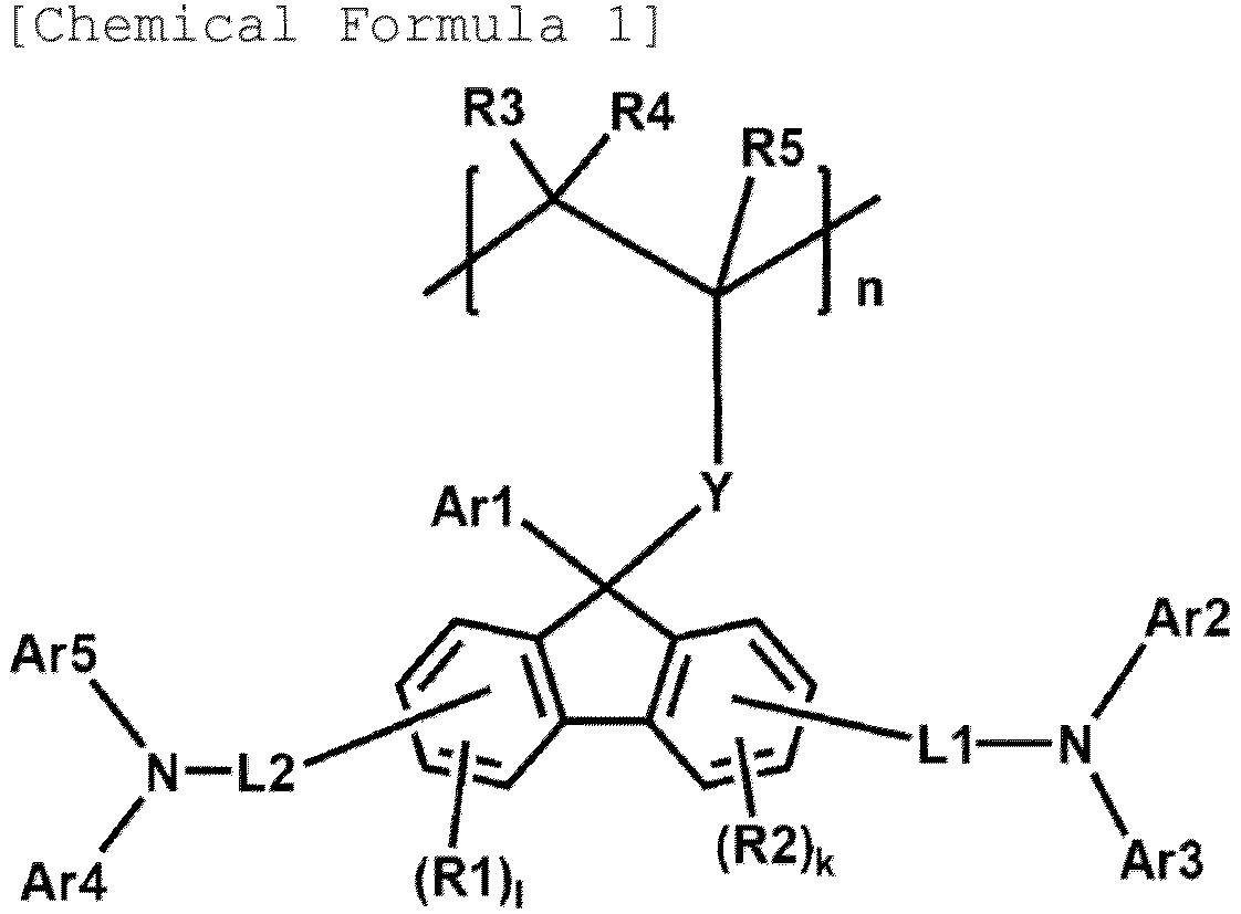
 Ar1 à Ar5 sont identiques les uns aux autres ou différents les uns des autres, et sont chacun indépendamment un groupe aryle substitué ou non substitué ;Ar2 et Ar3 sont facultativement liés l'un à l'autre pour former un hétérocycle substitué ou non substitué ;Ar4 et Ar5 sont facultativement liés l'un à l'autre pour former un hétérocycle substitué ou non substitué ;L1 et L2 sont identiques l'un à l'autre ou différents l'un de l'autre, et sont chacun indépendamment une liaison directe ; ou un groupe arylène substitué ou non substitué ;Y est choisi parmi les formules structurelles suivantes :

 dans les formules structurelles, R et R' sont identiques l'un à l'autre ou différents l'un de l'autre, et sont chacun indépendamment un groupe alkylène substitué ou non substitué ;R1 à R8 sont identiques les uns aux autres ou différents les uns des autres, et sont chacun indépendamment un hydrogène, ou un groupe alkyle substitué ou non substitué ;L3 est une liaison directe ; un groupe arylène substitué ou non substitué ; un groupe alkylène substitué ou non substitué ; un groupe alkylèneoxy substitué ou non substitué ; ou un groupe arylamine divalent substitué ou non substitué ;l et k sont chacun un nombre entier de 0 à 3, et lorsque l est égal ou supérieur à 2, les R1 sont identiques les uns aux autres ou différents les uns des autres, et lorsque k est égal ou supérieur à 2, les R2 sont identiques les uns aux autres ou différents les uns des autres ;j est un nombre entier de 1 à 3, et lorsque j est égal ou supérieur à 2, les L3 sont identiques les uns aux autres ou différents les uns des autres ;X est un groupe de durcissement ;n et m désignent un rapport molaire dans le polymère ; et0<n<1, 0<m<1, et m+n≤1.
 - Polymère selon la revendication 1, dans lequel le polymère incluant l'unité représentée par la Formule chimique 1 et l'unité représentée par la Formule chimique 2 présente un poids moléculaire moyen en nombre de 1 000 g/mol à 300 000 g/mol.
- Polymère selon la revendication 1, dans lequel Ar1 à Ar5 sont identiques les uns aux autres ou différents les uns des autres, et sont chacun indépendamment un groupe phényle substitué ou non substitué ; un groupe biphényle substitué ou non substitué ; ou un groupe fluorène substitué ou non substitué.
- Polymère selon la revendication 1, dans lequel L3 est une liaison directe ; un groupe phénylène non substitué ou substitué par un, deux ou plus de deux substituants choisis dans le groupe constitué d'un groupe alkyle, d'un groupe alcoxy et d'un groupe arylamine ; ou un groupe arylamine divalent.
- Polymère selon la revendication 1, dans lequel le groupe de durcissement est choisi parmi les formules structurelles suivantes :


- Polymère selon la revendication 1, dans lequel n est 0,6≤n<1, et m est 0<m≤0,4.
- Polymère selon la revendication 1, dans lequel le polymère incluant l'unité représentée par la Formule chimique 1 et l'unité représentée par la Formule chimique 2 est choisi parmi les formules structurelles suivantes :





- Composition de revêtement comprenant le polymère selon l'une quelconque des revendications 1 à 8.
- Composition de revêtement selon la revendication 9, qui est un dispositif électroluminescent organique.
- Dispositif électroluminescent organique comprenant :une première électrode ;une deuxième électrode disposée à l'opposé de la première électrode ; etune ou plusieurs couches de matière organique disposées entre la première électrode et la deuxième électrode,dans lequel une ou plusieurs couches des couches de matière organique incluent un produit durci de la composition de revêtement selon la revendication 8.
- Dispositif électroluminescent organique selon la revendication 10, dans lequel le matériau durci de la composition de revêtement est dans un état durci par un traitement thermique ou un traitement lumineux de la composition de revêtement.
- Dispositif électroluminescent organique selon la revendication 10, dans lequel la couche de matière organique incluant le matériau durci de la composition de revêtement est une couche de transfert de trous, une couche d'injection de trous, ou une couche effectuant simultanément un transfert de trous et une injection de trous.
- Dispositif électroluminescent organique selon la revendication 12, dans lequel la composition de revêtement inclut en outre un matériau de dopage p.
- Dispositif électroluminescent organique selon la revendication 13, dans lequel le matériau de dopage p inclut FaTCNQ ; ou un anion bore.
Applications Claiming Priority (2)
| Application Number | Priority Date | Filing Date | Title |
|---|---|---|---|
| KR1020180008801A KR102295248B1 (ko) | 2018-01-24 | 2018-01-24 | 중합체, 이를 포함하는 코팅 조성물 및 이를 이용한 유기 발광 소자 |
| PCT/KR2019/000841 WO2019146978A1 (fr) | 2018-01-24 | 2019-01-21 | Polymère, composition de revêtement le comprenant, et dispositif électroluminescent organique l'utilisant |
Publications (3)
| Publication Number | Publication Date |
|---|---|
| EP3677606A1 EP3677606A1 (fr) | 2020-07-08 |
| EP3677606A4 EP3677606A4 (fr) | 2021-01-13 |
| EP3677606B1 true EP3677606B1 (fr) | 2024-10-09 |
Family
ID=67394992
Family Applications (1)
| Application Number | Title | Priority Date | Filing Date |
|---|---|---|---|
| EP19743508.4A Active EP3677606B1 (fr) | 2018-01-24 | 2019-01-21 | Polymère, composition de revêtement le comprenant, et dispositif électroluminescent organique l'utilisant |
Country Status (7)
| Country | Link |
|---|---|
| US (1) | US11472901B2 (fr) |
| EP (1) | EP3677606B1 (fr) |
| JP (1) | JP6953058B2 (fr) |
| KR (1) | KR102295248B1 (fr) |
| CN (1) | CN111225930B (fr) |
| TW (1) | TWI705978B (fr) |
| WO (1) | WO2019146978A1 (fr) |
Families Citing this family (5)
| Publication number | Priority date | Publication date | Assignee | Title |
|---|---|---|---|---|
| JP7558612B2 (ja) * | 2020-01-13 | 2024-10-01 | エルジー・ケム・リミテッド | 重合体およびこれを用いた有機発光素子 |
| WO2021154041A1 (fr) * | 2020-01-31 | 2021-08-05 | 주식회사 엘지화학 | Composé, composition de revêtement le comprenant, dispositif électroluminescent organique l'utilisant, et procédé de fabrication associé |
| US20230140039A1 (en) * | 2020-03-27 | 2023-05-04 | Lg Chem, Ltd. | Novel Polymer and Organic Light Emitting Device Comprising Same |
| KR102841791B1 (ko) * | 2023-02-01 | 2025-08-01 | 부산대학교 산학협력단 | 유기 발광 재료용 모노머, 유기 발광 재료용 폴리머, 이의 제조 방법 및 이를 포함하는 유기 발광 소자 |
| KR102895605B1 (ko) * | 2024-04-01 | 2025-12-05 | 숭실대학교 산학협력단 | 정공 수송 재료, 이를 포함하는 유기 발광 소자, 정공 수송 재료 및 유기 발광 소자의 제조방법 |
Family Cites Families (24)
| Publication number | Priority date | Publication date | Assignee | Title |
|---|---|---|---|---|
| JP3791732B2 (ja) | 1998-09-11 | 2006-06-28 | 富士写真フイルム株式会社 | 有機エレクトロルミネツセンス素子材料およびそれを使用した有機エレクトロルミネツセンス素子 |
| JP2004303490A (ja) * | 2003-03-28 | 2004-10-28 | Tdk Corp | 有機el素子及び有機elディスプレイ |
| TW200517469A (en) | 2003-10-30 | 2005-06-01 | Nissan Chemical Ind Ltd | Charge-transporting compound, charge-transporting material, charge-transporting varnish, charge-transporting thin film, and organic electroluminescent device |
| KR101217899B1 (ko) * | 2003-11-17 | 2013-01-02 | 스미또모 가가꾸 가부시키가이샤 | 가교결합성 치환 플루오렌 화합물 및 그에 기초한 콘쥬게이트 올리고머 또는 중합체 |
| EP1915789B1 (fr) | 2005-08-17 | 2012-07-18 | Showa Denko K.K. | Dispositif organique electroluminescent utilisant un copolymere et un compose phosphorescent d'iridium |
| KR101258701B1 (ko) | 2005-11-24 | 2013-05-02 | 에스케이이노베이션 주식회사 | 9'-아릴-플루오렌-9'-일기가 도입된 아릴아민 단위를함유하는 유기 전기발광고분자 및 이를 이용한전기발광소자 |
| US8404362B2 (en) | 2007-07-13 | 2013-03-26 | Showa Denko K.K. | Organic light-emitting element using triazine ring-containing polymer compound |
| JP5696662B2 (ja) | 2009-06-01 | 2015-04-08 | 日立化成株式会社 | 有機エレクトロルミネセンス素子、表示素子、照明装置および表示装置 |
| KR101311933B1 (ko) | 2009-12-29 | 2013-09-27 | 제일모직주식회사 | 전도성 고분자 중합체, 전도성 고분자 조성물, 전도성 고분자 조성물막 및 이를 이용한 유기광전소자 |
| EP2692751B1 (fr) | 2011-03-31 | 2015-09-23 | Nippon Steel & Sumikin Chemical Co., Ltd. | Polymère pour des éléments électroluminescents organiques et élément électroluminescent organique utilisant un produit durci de ce polymère |
| KR101463298B1 (ko) | 2011-04-01 | 2014-11-20 | 주식회사 엘지화학 | 새로운 유기 발광 소자 재료 및 이를 이용한 유기 발광 소자 |
| EP2610240A1 (fr) | 2011-12-28 | 2013-07-03 | Solvay Sa | Composés réticulables d'arylamine |
| JP2016119320A (ja) * | 2013-03-01 | 2016-06-30 | 出光興産株式会社 | 重合性単量体、その重合体を含む有機デバイス用材料、正孔注入輸送材料、及び有機エレクトロルミネッセンス素子用材料、並びに有機エレクトロルミネッセンス素子 |
| CN106459409B (zh) | 2014-03-03 | 2019-08-16 | 三菱化学株式会社 | 聚合物、有机场致发光元件用组合物、有机场致发光元件、有机el显示装置及有机el照明 |
| EP3085693A1 (fr) * | 2015-04-20 | 2016-10-26 | Solvay SA | Nouveaux dérivés 3,6-substitués de fluorène |
| EP3098085A1 (fr) | 2015-05-28 | 2016-11-30 | Schoeller Technocell GmbH & Co. KG | Matériau de transfert pour l'impression par sublimation |
| JP6652351B2 (ja) | 2015-09-01 | 2020-02-19 | 三星電子株式会社Samsung Electronics Co.,Ltd. | アミノフルオレンポリマー、有機エレクトロルミネッセンス素子用材料、および有機エレクトロルミネッセンス素子 |
| EP3138858B1 (fr) | 2015-09-01 | 2019-10-30 | Samsung Electronics Co., Ltd. | Polymère amino-fluorène et dispositif électroluminescent organique l'incluant |
| EP3351576B1 (fr) * | 2015-09-18 | 2020-05-06 | Sumitomo Chemical Company, Limited | Composé polymère et élément électroluminescent utilisant ce dernier |
| US20210210691A1 (en) * | 2015-12-24 | 2021-07-08 | Dow Global Technologies Llc | Polymeric layer and organic electronic device comprising same. |
| JP6659357B2 (ja) | 2015-12-28 | 2020-03-04 | 三星電子株式会社Samsung Electronics Co.,Ltd. | 共重合体、有機エレクトロルミネッセンス素子材料、有機エレクトロルミネッセンス素子製造用組成物および有機エレクトロルミネッセンス素子 |
| JP7068199B2 (ja) | 2016-06-28 | 2022-05-16 | ダウ グローバル テクノロジーズ エルエルシー | 量子ドット発光素子 |
| CN107556297B (zh) | 2017-09-29 | 2020-09-04 | 中节能万润股份有限公司 | 一种氧杂蒽类有机化合物及其应用 |
| WO2019126548A1 (fr) | 2017-12-22 | 2019-06-27 | Energy Everywhere, Inc. | Matériaux de transport de trous ioniques fusionnés et réticulables pour cellules solaires en pérovskite |
-
2018
- 2018-01-24 KR KR1020180008801A patent/KR102295248B1/ko active Active
-
2019
- 2019-01-21 CN CN201980005151.7A patent/CN111225930B/zh active Active
- 2019-01-21 EP EP19743508.4A patent/EP3677606B1/fr active Active
- 2019-01-21 WO PCT/KR2019/000841 patent/WO2019146978A1/fr not_active Ceased
- 2019-01-21 JP JP2020518754A patent/JP6953058B2/ja active Active
- 2019-01-21 US US16/652,294 patent/US11472901B2/en active Active
- 2019-01-23 TW TW108102456A patent/TWI705978B/zh active
Also Published As
| Publication number | Publication date |
|---|---|
| JP6953058B2 (ja) | 2021-10-27 |
| TW201934594A (zh) | 2019-09-01 |
| TWI705978B (zh) | 2020-10-01 |
| KR102295248B1 (ko) | 2021-08-27 |
| KR20190090211A (ko) | 2019-08-01 |
| WO2019146978A1 (fr) | 2019-08-01 |
| CN111225930A (zh) | 2020-06-02 |
| CN111225930B (zh) | 2022-12-23 |
| US20200239610A1 (en) | 2020-07-30 |
| EP3677606A4 (fr) | 2021-01-13 |
| JP2020536148A (ja) | 2020-12-10 |
| EP3677606A1 (fr) | 2020-07-08 |
| US11472901B2 (en) | 2022-10-18 |
Similar Documents
| Publication | Publication Date | Title |
|---|---|---|
| EP3511382B1 (fr) | Diode électroluminescente organique | |
| EP3431467B1 (fr) | Dérivé de carbazole et élément électroluminescent organique le comprenant | |
| EP3686943B1 (fr) | Diode électroluminescente organique | |
| EP3763750B1 (fr) | Polymère, monomère, composition de revêtement les comprenant, et dispositif électroluminescent organique faisant appel à celui-ci | |
| CN109863135B (zh) | 化合物、包含其的涂覆组合物、使用其的有机发光器件和其制备方法 | |
| EP3677606B1 (fr) | Polymère, composition de revêtement le comprenant, et dispositif électroluminescent organique l'utilisant | |
| EP3680261B1 (fr) | Polymère, composition de revêtement le comprenant, et élément électroluminescent organique l'utilisant | |
| EP3683208B1 (fr) | Composé, composition de revêtement le comprenant, et dispositif électroluminescent organique | |
| EP3680262B1 (fr) | Polymère, composition de revêtement le comprenant, et diode électroluminescente organique l'utilisant | |
| KR20180092893A (ko) | 화합물, 이를 포함하는 코팅 조성물 및 이를 이용한 유기 발광 소자 | |
| JP6953059B2 (ja) | 重合体、これを含むコーティング組成物およびこれを用いた有機発光素子 | |
| EP3677602B1 (fr) | Polymère, composition de revêtement le comprenant, et dispositif électroluminescent organique l'utilisant | |
| KR102845761B1 (ko) | 중합체, 이를 포함하는 코팅 조성물 및 이를 이용한 유기 발광 소자 |
Legal Events
| Date | Code | Title | Description |
|---|---|---|---|
| STAA | Information on the status of an ep patent application or granted ep patent |
Free format text: STATUS: THE INTERNATIONAL PUBLICATION HAS BEEN MADE |
|
| PUAI | Public reference made under article 153(3) epc to a published international application that has entered the european phase |
Free format text: ORIGINAL CODE: 0009012 |
|
| STAA | Information on the status of an ep patent application or granted ep patent |
Free format text: STATUS: REQUEST FOR EXAMINATION WAS MADE |
|
| 17P | Request for examination filed |
Effective date: 20200403 |
|
| AK | Designated contracting states |
Kind code of ref document: A1 Designated state(s): AL AT BE BG CH CY CZ DE DK EE ES FI FR GB GR HR HU IE IS IT LI LT LU LV MC MK MT NL NO PL PT RO RS SE SI SK SM TR |
|
| AX | Request for extension of the european patent |
Extension state: BA ME |
|
| A4 | Supplementary search report drawn up and despatched |
Effective date: 20201211 |
|
| RIC1 | Information provided on ipc code assigned before grant |
Ipc: C08F 212/14 20060101ALI20201207BHEP Ipc: H01L 51/50 20060101ALI20201207BHEP Ipc: H01L 51/52 20060101ALI20201207BHEP Ipc: C09D 125/18 20060101ALI20201207BHEP Ipc: C08F 212/32 20060101AFI20201207BHEP |
|
| DAV | Request for validation of the european patent (deleted) | ||
| DAX | Request for extension of the european patent (deleted) | ||
| STAA | Information on the status of an ep patent application or granted ep patent |
Free format text: STATUS: EXAMINATION IS IN PROGRESS |
|
| 17Q | First examination report despatched |
Effective date: 20211110 |
|
| GRAP | Despatch of communication of intention to grant a patent |
Free format text: ORIGINAL CODE: EPIDOSNIGR1 |
|
| STAA | Information on the status of an ep patent application or granted ep patent |
Free format text: STATUS: GRANT OF PATENT IS INTENDED |
|
| RIC1 | Information provided on ipc code assigned before grant |
Ipc: H05B 33/00 20060101ALI20240430BHEP Ipc: C09D 125/18 20060101ALI20240430BHEP Ipc: C08F 212/14 20060101ALI20240430BHEP Ipc: C08F 212/32 20060101AFI20240430BHEP |
|
| INTG | Intention to grant announced |
Effective date: 20240521 |
|
| GRAS | Grant fee paid |
Free format text: ORIGINAL CODE: EPIDOSNIGR3 |
|
| GRAA | (expected) grant |
Free format text: ORIGINAL CODE: 0009210 |
|
| STAA | Information on the status of an ep patent application or granted ep patent |
Free format text: STATUS: THE PATENT HAS BEEN GRANTED |
|
| AK | Designated contracting states |
Kind code of ref document: B1 Designated state(s): AL AT BE BG CH CY CZ DE DK EE ES FI FR GB GR HR HU IE IS IT LI LT LU LV MC MK MT NL NO PL PT RO RS SE SI SK SM TR |
|
| REG | Reference to a national code |
Ref country code: CH Ref legal event code: EP |
|
| REG | Reference to a national code |
Ref country code: DE Ref legal event code: R096 Ref document number: 602019060084 Country of ref document: DE |
|
| REG | Reference to a national code |
Ref country code: IE Ref legal event code: FG4D |
|
| REG | Reference to a national code |
Ref country code: LT Ref legal event code: MG9D |
|
| REG | Reference to a national code |
Ref country code: NL Ref legal event code: MP Effective date: 20241009 |
|
| REG | Reference to a national code |
Ref country code: AT Ref legal event code: MK05 Ref document number: 1730532 Country of ref document: AT Kind code of ref document: T Effective date: 20241009 |
|
| PG25 | Lapsed in a contracting state [announced via postgrant information from national office to epo] |
Ref country code: NL Free format text: LAPSE BECAUSE OF FAILURE TO SUBMIT A TRANSLATION OF THE DESCRIPTION OR TO PAY THE FEE WITHIN THE PRESCRIBED TIME-LIMIT Effective date: 20241009 |
|
| PG25 | Lapsed in a contracting state [announced via postgrant information from national office to epo] |
Ref country code: NL Free format text: LAPSE BECAUSE OF FAILURE TO SUBMIT A TRANSLATION OF THE DESCRIPTION OR TO PAY THE FEE WITHIN THE PRESCRIBED TIME-LIMIT Effective date: 20241009 |
|
| PG25 | Lapsed in a contracting state [announced via postgrant information from national office to epo] |
Ref country code: IS Free format text: LAPSE BECAUSE OF FAILURE TO SUBMIT A TRANSLATION OF THE DESCRIPTION OR TO PAY THE FEE WITHIN THE PRESCRIBED TIME-LIMIT Effective date: 20250209 Ref country code: PT Free format text: LAPSE BECAUSE OF FAILURE TO SUBMIT A TRANSLATION OF THE DESCRIPTION OR TO PAY THE FEE WITHIN THE PRESCRIBED TIME-LIMIT Effective date: 20250210 Ref country code: HR Free format text: LAPSE BECAUSE OF FAILURE TO SUBMIT A TRANSLATION OF THE DESCRIPTION OR TO PAY THE FEE WITHIN THE PRESCRIBED TIME-LIMIT Effective date: 20241009 |
|
| PG25 | Lapsed in a contracting state [announced via postgrant information from national office to epo] |
Ref country code: FI Free format text: LAPSE BECAUSE OF FAILURE TO SUBMIT A TRANSLATION OF THE DESCRIPTION OR TO PAY THE FEE WITHIN THE PRESCRIBED TIME-LIMIT Effective date: 20241009 |
|
| PG25 | Lapsed in a contracting state [announced via postgrant information from national office to epo] |
Ref country code: BG Free format text: LAPSE BECAUSE OF FAILURE TO SUBMIT A TRANSLATION OF THE DESCRIPTION OR TO PAY THE FEE WITHIN THE PRESCRIBED TIME-LIMIT Effective date: 20241009 |
|
| PG25 | Lapsed in a contracting state [announced via postgrant information from national office to epo] |
Ref country code: ES Free format text: LAPSE BECAUSE OF FAILURE TO SUBMIT A TRANSLATION OF THE DESCRIPTION OR TO PAY THE FEE WITHIN THE PRESCRIBED TIME-LIMIT Effective date: 20241009 |
|
| PG25 | Lapsed in a contracting state [announced via postgrant information from national office to epo] |
Ref country code: NO Free format text: LAPSE BECAUSE OF FAILURE TO SUBMIT A TRANSLATION OF THE DESCRIPTION OR TO PAY THE FEE WITHIN THE PRESCRIBED TIME-LIMIT Effective date: 20250109 |
|
| PG25 | Lapsed in a contracting state [announced via postgrant information from national office to epo] |
Ref country code: LV Free format text: LAPSE BECAUSE OF FAILURE TO SUBMIT A TRANSLATION OF THE DESCRIPTION OR TO PAY THE FEE WITHIN THE PRESCRIBED TIME-LIMIT Effective date: 20241009 Ref country code: GR Free format text: LAPSE BECAUSE OF FAILURE TO SUBMIT A TRANSLATION OF THE DESCRIPTION OR TO PAY THE FEE WITHIN THE PRESCRIBED TIME-LIMIT Effective date: 20250110 Ref country code: AT Free format text: LAPSE BECAUSE OF FAILURE TO SUBMIT A TRANSLATION OF THE DESCRIPTION OR TO PAY THE FEE WITHIN THE PRESCRIBED TIME-LIMIT Effective date: 20241009 |
|
| PG25 | Lapsed in a contracting state [announced via postgrant information from national office to epo] |
Ref country code: PL Free format text: LAPSE BECAUSE OF FAILURE TO SUBMIT A TRANSLATION OF THE DESCRIPTION OR TO PAY THE FEE WITHIN THE PRESCRIBED TIME-LIMIT Effective date: 20241009 |
|
| PG25 | Lapsed in a contracting state [announced via postgrant information from national office to epo] |
Ref country code: RS Free format text: LAPSE BECAUSE OF FAILURE TO SUBMIT A TRANSLATION OF THE DESCRIPTION OR TO PAY THE FEE WITHIN THE PRESCRIBED TIME-LIMIT Effective date: 20250109 |
|
| PG25 | Lapsed in a contracting state [announced via postgrant information from national office to epo] |
Ref country code: SM Free format text: LAPSE BECAUSE OF FAILURE TO SUBMIT A TRANSLATION OF THE DESCRIPTION OR TO PAY THE FEE WITHIN THE PRESCRIBED TIME-LIMIT Effective date: 20241009 |
|
| PG25 | Lapsed in a contracting state [announced via postgrant information from national office to epo] |
Ref country code: DK Free format text: LAPSE BECAUSE OF FAILURE TO SUBMIT A TRANSLATION OF THE DESCRIPTION OR TO PAY THE FEE WITHIN THE PRESCRIBED TIME-LIMIT Effective date: 20241009 |
|
| REG | Reference to a national code |
Ref country code: DE Ref legal event code: R097 Ref document number: 602019060084 Country of ref document: DE |
|
| PG25 | Lapsed in a contracting state [announced via postgrant information from national office to epo] |
Ref country code: EE Free format text: LAPSE BECAUSE OF FAILURE TO SUBMIT A TRANSLATION OF THE DESCRIPTION OR TO PAY THE FEE WITHIN THE PRESCRIBED TIME-LIMIT Effective date: 20241009 |
|
| PG25 | Lapsed in a contracting state [announced via postgrant information from national office to epo] |
Ref country code: RO Free format text: LAPSE BECAUSE OF FAILURE TO SUBMIT A TRANSLATION OF THE DESCRIPTION OR TO PAY THE FEE WITHIN THE PRESCRIBED TIME-LIMIT Effective date: 20241009 |
|
| PG25 | Lapsed in a contracting state [announced via postgrant information from national office to epo] |
Ref country code: SK Free format text: LAPSE BECAUSE OF FAILURE TO SUBMIT A TRANSLATION OF THE DESCRIPTION OR TO PAY THE FEE WITHIN THE PRESCRIBED TIME-LIMIT Effective date: 20241009 |
|
| PG25 | Lapsed in a contracting state [announced via postgrant information from national office to epo] |
Ref country code: CZ Free format text: LAPSE BECAUSE OF FAILURE TO SUBMIT A TRANSLATION OF THE DESCRIPTION OR TO PAY THE FEE WITHIN THE PRESCRIBED TIME-LIMIT Effective date: 20241009 |
|
| PG25 | Lapsed in a contracting state [announced via postgrant information from national office to epo] |
Ref country code: IT Free format text: LAPSE BECAUSE OF FAILURE TO SUBMIT A TRANSLATION OF THE DESCRIPTION OR TO PAY THE FEE WITHIN THE PRESCRIBED TIME-LIMIT Effective date: 20241009 |
|
| PLBE | No opposition filed within time limit |
Free format text: ORIGINAL CODE: 0009261 |
|
| STAA | Information on the status of an ep patent application or granted ep patent |
Free format text: STATUS: NO OPPOSITION FILED WITHIN TIME LIMIT |
|
| REG | Reference to a national code |
Ref country code: CH Ref legal event code: PL |
|
| PG25 | Lapsed in a contracting state [announced via postgrant information from national office to epo] |
Ref country code: SE Free format text: LAPSE BECAUSE OF FAILURE TO SUBMIT A TRANSLATION OF THE DESCRIPTION OR TO PAY THE FEE WITHIN THE PRESCRIBED TIME-LIMIT Effective date: 20241009 |
|
| PG25 | Lapsed in a contracting state [announced via postgrant information from national office to epo] |
Ref country code: MC Free format text: LAPSE BECAUSE OF FAILURE TO SUBMIT A TRANSLATION OF THE DESCRIPTION OR TO PAY THE FEE WITHIN THE PRESCRIBED TIME-LIMIT Effective date: 20241009 Ref country code: LU Free format text: LAPSE BECAUSE OF NON-PAYMENT OF DUE FEES Effective date: 20250121 |
|
| 26N | No opposition filed |
Effective date: 20250710 |
|
| GBPC | Gb: european patent ceased through non-payment of renewal fee |
Effective date: 20250121 |
|
| PG25 | Lapsed in a contracting state [announced via postgrant information from national office to epo] |
Ref country code: GB Free format text: LAPSE BECAUSE OF NON-PAYMENT OF DUE FEES Effective date: 20250121 Ref country code: BE Free format text: LAPSE BECAUSE OF NON-PAYMENT OF DUE FEES Effective date: 20250131 |
|
| PG25 | Lapsed in a contracting state [announced via postgrant information from national office to epo] |
Ref country code: CH Free format text: LAPSE BECAUSE OF NON-PAYMENT OF DUE FEES Effective date: 20250131 |
|
| REG | Reference to a national code |
Ref country code: BE Ref legal event code: MM Effective date: 20250131 |
|
| PGFP | Annual fee paid to national office [announced via postgrant information from national office to epo] |
Ref country code: FR Payment date: 20251223 Year of fee payment: 8 |
|
| PG25 | Lapsed in a contracting state [announced via postgrant information from national office to epo] |
Ref country code: IE Free format text: LAPSE BECAUSE OF NON-PAYMENT OF DUE FEES Effective date: 20250121 |
|
| PGFP | Annual fee paid to national office [announced via postgrant information from national office to epo] |
Ref country code: DE Payment date: 20251222 Year of fee payment: 8 |