EP3677885A1 - Ungekühlter thermischer bildgeber - Google Patents
Ungekühlter thermischer bildgeber Download PDFInfo
- Publication number
- EP3677885A1 EP3677885A1 EP19150221.0A EP19150221A EP3677885A1 EP 3677885 A1 EP3677885 A1 EP 3677885A1 EP 19150221 A EP19150221 A EP 19150221A EP 3677885 A1 EP3677885 A1 EP 3677885A1
- Authority
- EP
- European Patent Office
- Prior art keywords
- chips
- rows
- row
- pair
- array
- Prior art date
- Legal status (The legal status is an assumption and is not a legal conclusion. Google has not performed a legal analysis and makes no representation as to the accuracy of the status listed.)
- Granted
Links
Images


Classifications
-
- G—PHYSICS
- G01—MEASURING; TESTING
- G01J—MEASUREMENT OF INTENSITY, VELOCITY, SPECTRAL CONTENT, POLARISATION, PHASE OR PULSE CHARACTERISTICS OF INFRARED, VISIBLE OR ULTRAVIOLET LIGHT; COLORIMETRY; RADIATION PYROMETRY
- G01J5/00—Radiation pyrometry, e.g. infrared or optical thermometry
- G01J5/007—Radiation pyrometry, e.g. infrared or optical thermometry for earth observation
-
- B—PERFORMING OPERATIONS; TRANSPORTING
- B64—AIRCRAFT; AVIATION; COSMONAUTICS
- B64G—COSMONAUTICS; VEHICLES OR EQUIPMENT THEREFOR
- B64G1/00—Cosmonautic vehicles
- B64G1/10—Artificial satellites; Systems of such satellites; Interplanetary vehicles
-
- B—PERFORMING OPERATIONS; TRANSPORTING
- B64—AIRCRAFT; AVIATION; COSMONAUTICS
- B64G—COSMONAUTICS; VEHICLES OR EQUIPMENT THEREFOR
- B64G1/00—Cosmonautic vehicles
- B64G1/22—Parts of, or equipment specially adapted for fitting in or to, cosmonautic vehicles
- B64G1/66—Arrangements or adaptations of apparatus or instruments, not otherwise provided for
-
- G—PHYSICS
- G01—MEASURING; TESTING
- G01J—MEASUREMENT OF INTENSITY, VELOCITY, SPECTRAL CONTENT, POLARISATION, PHASE OR PULSE CHARACTERISTICS OF INFRARED, VISIBLE OR ULTRAVIOLET LIGHT; COLORIMETRY; RADIATION PYROMETRY
- G01J5/00—Radiation pyrometry, e.g. infrared or optical thermometry
- G01J5/02—Constructional details
- G01J5/08—Optical arrangements
- G01J5/0801—Means for wavelength selection or discrimination
- G01J5/0802—Optical filters
- G01J5/08021—Notch filters
-
- G—PHYSICS
- G01—MEASURING; TESTING
- G01J—MEASUREMENT OF INTENSITY, VELOCITY, SPECTRAL CONTENT, POLARISATION, PHASE OR PULSE CHARACTERISTICS OF INFRARED, VISIBLE OR ULTRAVIOLET LIGHT; COLORIMETRY; RADIATION PYROMETRY
- G01J5/00—Radiation pyrometry, e.g. infrared or optical thermometry
- G01J5/02—Constructional details
- G01J5/08—Optical arrangements
- G01J5/0806—Focusing or collimating elements, e.g. lenses or concave mirrors
-
- G—PHYSICS
- G01—MEASURING; TESTING
- G01J—MEASUREMENT OF INTENSITY, VELOCITY, SPECTRAL CONTENT, POLARISATION, PHASE OR PULSE CHARACTERISTICS OF INFRARED, VISIBLE OR ULTRAVIOLET LIGHT; COLORIMETRY; RADIATION PYROMETRY
- G01J5/00—Radiation pyrometry, e.g. infrared or optical thermometry
- G01J5/10—Radiation pyrometry, e.g. infrared or optical thermometry using electric radiation detectors
- G01J5/12—Radiation pyrometry, e.g. infrared or optical thermometry using electric radiation detectors using thermoelectric elements, e.g. thermocouples
-
- H—ELECTRICITY
- H04—ELECTRIC COMMUNICATION TECHNIQUE
- H04N—PICTORIAL COMMUNICATION, e.g. TELEVISION
- H04N13/00—Stereoscopic video systems; Multi-view video systems; Details thereof
- H04N13/20—Image signal generators
- H04N13/204—Image signal generators using stereoscopic image cameras
- H04N13/207—Image signal generators using stereoscopic image cameras using a single two-dimensional [2D] image sensor
- H04N13/218—Image signal generators using stereoscopic image cameras using a single two-dimensional [2D] image sensor using spatial multiplexing
-
- H—ELECTRICITY
- H04—ELECTRIC COMMUNICATION TECHNIQUE
- H04N—PICTORIAL COMMUNICATION, e.g. TELEVISION
- H04N23/00—Cameras or camera modules comprising electronic image sensors; Control thereof
- H04N23/20—Cameras or camera modules comprising electronic image sensors; Control thereof for generating image signals from infrared radiation only
- H04N23/23—Cameras or camera modules comprising electronic image sensors; Control thereof for generating image signals from infrared radiation only from thermal infrared radiation
-
- H—ELECTRICITY
- H10—SEMICONDUCTOR DEVICES; ELECTRIC SOLID-STATE DEVICES NOT OTHERWISE PROVIDED FOR
- H10N—ELECTRIC SOLID-STATE DEVICES NOT OTHERWISE PROVIDED FOR
- H10N19/00—Integrated devices, or assemblies of multiple devices, comprising at least one thermoelectric or thermomagnetic element covered by groups H10N10/00 - H10N15/00
-
- G—PHYSICS
- G01—MEASURING; TESTING
- G01J—MEASUREMENT OF INTENSITY, VELOCITY, SPECTRAL CONTENT, POLARISATION, PHASE OR PULSE CHARACTERISTICS OF INFRARED, VISIBLE OR ULTRAVIOLET LIGHT; COLORIMETRY; RADIATION PYROMETRY
- G01J5/00—Radiation pyrometry, e.g. infrared or optical thermometry
- G01J2005/0077—Imaging
-
- G—PHYSICS
- G01—MEASURING; TESTING
- G01J—MEASUREMENT OF INTENSITY, VELOCITY, SPECTRAL CONTENT, POLARISATION, PHASE OR PULSE CHARACTERISTICS OF INFRARED, VISIBLE OR ULTRAVIOLET LIGHT; COLORIMETRY; RADIATION PYROMETRY
- G01J5/00—Radiation pyrometry, e.g. infrared or optical thermometry
- G01J5/10—Radiation pyrometry, e.g. infrared or optical thermometry using electric radiation detectors
- G01J5/12—Radiation pyrometry, e.g. infrared or optical thermometry using electric radiation detectors using thermoelectric elements, e.g. thermocouples
- G01J2005/123—Thermoelectric array
-
- H—ELECTRICITY
- H04—ELECTRIC COMMUNICATION TECHNIQUE
- H04N—PICTORIAL COMMUNICATION, e.g. TELEVISION
- H04N13/00—Stereoscopic video systems; Multi-view video systems; Details thereof
- H04N13/20—Image signal generators
- H04N13/204—Image signal generators using stereoscopic image cameras
- H04N13/243—Image signal generators using stereoscopic image cameras using three or more two-dimensional [2D] image sensors
-
- H—ELECTRICITY
- H04—ELECTRIC COMMUNICATION TECHNIQUE
- H04N—PICTORIAL COMMUNICATION, e.g. TELEVISION
- H04N13/00—Stereoscopic video systems; Multi-view video systems; Details thereof
- H04N2013/0074—Stereoscopic image analysis
- H04N2013/0092—Image segmentation from stereoscopic image signals
Definitions
- This application relates to thermal imagers, such as infrared (IR) cameras, for example.
- the application relates to uncooled thermal imagers, and more particularly, to uncooled thermal imagers that are suitable for use in satellites (e.g., nanosatellites, such as Cubesats), airplanes, or unmanned aerial vehicles.
- satellites e.g., nanosatellites, such as Cubesats
- airplanes e.g., airplanes, or unmanned aerial vehicles.
- the spectral range (wavelength range) from 8 ⁇ m to 13 ⁇ m as well as 4 ⁇ 0,5 ⁇ m is not (or just minimally) absorbed by Earth's atmosphere and is therefore particularly suited for measuring the temperature of Earth's surface from space (e.g., from an orbit around Earth). Thus, most meteorological satellites use this spectral range for the purpose of temperature measurements.
- thermal imagers e.g., IR cameras
- Active cooling necessitates large power consumption and active thermal management needs to be provided to discharge the cooling power (e.g., heat from a Peltier element).
- the present disclosure proposes a thermal imager, a satellite having a thermal imager, and a method of operating a thermal imager aboard a satellite, having the features of the respective independent claims.
- the thermal imager may be an infrared camera, for example.
- the thermal imager may include a lens assembly.
- the lens assembly may include a first lens and a second lens arranged on a common optical axis.
- the lens assembly may allow passage of (thermal) radiation in a given wavelength range.
- the lens assembly may be transparent in the IR range, for example for wavelengths from 8 ⁇ m-13 ⁇ m or (at least) 8 ⁇ m-12 ⁇ m.
- the lens assembly may additionally be transparent in a wavelength range around 4 ⁇ m or any other value between 2 ⁇ m and 20 ⁇ m.
- the thermal imager may further include an array of integrated circuit (IC) chips that is arranged in a field of view of the lens array.
- IC integrated circuit
- Each IC chip may include an array of thermopile devices. Accordingly, the array of IC chips may also be referred to as an array of arrays of thermopile devices.
- the array of IC chips may act as an image sensor (camera sensor).
- the thermal imager may further include a filter assembly comprising one or more wavelength filters.
- the wavelength filters may be bandpass filters, for example.
- the IC chips may be arranged in three or more parallel rows of IC chips that include a pair of non-adjacent rows of IC chips and one or more rows of IC chips other than the pair of non-adjacent rows of IC chips.
- the pair of non-adjacent rows of IC chips may be the outer two rows of the array of IC chips.
- the one more rows other than the pair of non-adjacent rows of IC chips may be the intermediate (or inner) rows of the array of IC chips.
- the rows of IC chips may be equidistant.
- IC chips within each row of IC chips may be equidistant.
- the IC chips in the array of IC chips may be arranged at the vertices of a regular rectangular grid.
- the filter assembly may be arranged between the array of IC chips and the lens assembly.
- the filter assembly may include a respective wavelength filter for at least one of the first to third rows of IC chips.
- the wavelength filters may be each (spatially) aligned with their respective row of IC chips (e.g., to substantially cover (only) the respective row of IC chips when seen from the lens assembly).
- the one or more wavelength filters may be transparent in a portion of a wavelength range of radiation that can pass through the lens assembly (and may be non-transparent in another portion of the wavelength range of radiation that can pass through the lens assembly). That is, the wavelength filters may filter (block) a portion of the wavelength range of (thermal) radiation that can pass through the lens assembly.
- the filter assembly may be further configured such that radiation of the same wavelength range can pass to the rows of IC chips in the pair of non-adjacent rows of IC chips, and such that the wavelength range of radiation that can pass to the rows of IC chips in the pair of non-adjacent rows of IC chips is different from a wavelength range of radiation that can pass to the one or more rows of IC chips other than the pair of non-adjacent rows of IC chips.
- the three or more parallel rows of IC chips may include first to third rows of IC chips.
- the second row of IC chips may be arranged at an intermediate position between the first and third rows of IC chips.
- the filter assembly may be further configured such that a wavelength range of radiation that can pass to the first row of IC chips is the same as a wavelength range of radiation that can pass to the third row of IC chips, and is different from a wavelength range of radiation that can pass to the second row of IC chips.
- the first and third rows may receive filtered radiation, while there is no filter for the second row, or vice versa.
- the array of IC chips comprises four rows of IC chips, with the pair of outer rows receiving radiation of the same wavelength range.
- radiation is intended to mean thermal radiation, unless indicated otherwise.
- thermopile arrays for building up the image sensor of the thermal imager, active cooling is not necessary. Thereby, the power consumption of the proposed thermal imager can be reduced to less than one tenth of the power consumption of conventional thermal imagers. Likewise, the absence of active cooling allows for a more compact design of the thermal imager, making it a suitable candidate for use in nanosatellites, small aircraft, or small unmanned aerial vehicles.
- the proposed thermal imager allows to capture two-dimensional thermal images of Earth's surface.
- thermal resolution can be achieved that is more than sufficient for the intended purpose of measuring temperatures on Earth's surface for meteorological applications.
- the wavelength range of radiation that can pass to the rows of IC chips in the pair of non-adjacent rows of IC chips may span at least two thirds of the wavelength range of (thermal) radiation that can pass through the lens assembly.
- the wavelength range of radiation that can pass to the rows of IC chips in the pair of non-adjacent rows of IC chips may span at least 90 percent (%) of the wavelength range of radiation that can pass through the lens assembly.
- the wavelength range of radiation that can pass to the rows of IC chips in the pair of non-adjacent rows of IC chips may be larger than the wavelength range of radiation that can pass to the one or more rows of IC chips other than the pair of non-adjacent rows of IC chips (e.g., the second row of IC chips) by at least 50 percent.
- the wavelength range of radiation that can pass to the rows of IC chips in the pair of non-adjacent rows of IC chips may be larger than the wavelength range of radiation that can pass to the one or more rows of IC chips other than the pair of non-adjacent rows of IC chips (e.g., the second row of IC chips) by 100 percent (%).
- the wavelength range of radiation that can pass to the rows of IC chips in the pair of non-adjacent rows of IC chips may span the full wavelength range of radiation that can pass through the lens assembly. Accordingly, radiation that can pass to the rows of IC chips in the pair of non-adjacent rows of IC chips (e.g., the first and third rows of IC chips) may not be filtered by the filter assembly (i.e., there may not be a corresponding wavelength filter for these rows of IC chips).
- At least two rows of IC chips that are spaced apart from each other receive radiation in the same, broad, wavelength range.
- Readout signals (thermal images) from these rows of IC chips can therefore be used for applying stereoscopy.
- the row or rows of IC chips that receive radiation in a narrower wavelength range can be used, for example, calculating the temperature of Earth's surface.
- the array of IC chips may include at least two inner rows of IC chips that are arranged at respective intermediate positions between the rows of IC chips in the pair of non-adjacent rows of IC chips.
- the array of IC chips may include, in addition to the first, second, and third rows of IC chips, a fourth row of IC chips arranged at a position between the first and third rows of IC chips.
- the filter assembly may comprise a respective wavelength filter for each of the at least two inner rows of IC chips (e.g., for the second and fourths rows of IC chips).
- Wavelength ranges of radiation that can pass through the respective wavelength filters for the at least two inner rows of IC chips may be different from each other. In an ideal case, these wavelength ranges may be substantially disjoint.
- the thermal imager comprises two rows of IC chips that receive radiation in comparatively narrow (filtered) wavelength ranges. Readout signals (thermal images) from these rows can be used for accurately calculating the temperature on Earth's surface.
- a wavelength range of radiation that can pass through the lens assembly may be partitioned by the wavelength filters of the filter assembly.
- the wavelength ranges in which the wavelength filters are transparent may be substantially disjoint and may add up to the full wavelength range. If for example the full wavelength range (wavelength range of radiation that can pass through the lens assembly) is 8 ⁇ m-12 ⁇ m, the passbands of the wavelength filters for the second and fourth rows of IC chips may be 8 ⁇ m-10 ⁇ m and 10 ⁇ m-12 ⁇ m, respectively.
- Providing four rows of IC chips that are sensitive in such disjoint wavelength ranges allows to accurately calculate the temperature on Earth's surface. Moreover, for disjoint wavelength ranges, additional information can be inferred by taking differences between thermal images from different rows of IC chips.
- the array of IC chips may be a rectangular (e.g., quadratic) or circular array.
- the rows of IC chips may have different lengths (in terms of a number of IC chips in respective rows).
- the number of IC chips per row can be different from the number of rows of IC chips in the array of IC chips.
- the shape of the thermal imager can be adapted to the enclosure in a satellite, airplane, or unmanned aerial vehicle that is intended to carry the thermal imager.
- the filter assembly may be arranged at a predetermined distance from the array of IC chips.
- the distance may be in the range from 1 mm to 10 mm, for example.
- the filter assembly may be spaced without contact from the array of IC chips.
- the thermal imager may be suitable for use in at least one of a satellite, an airplane, or an unmanned aerial vehicle.
- the satellite may be a nanosatellite, such as a Cubesat (e.g., 3U Cubesat), for example. This may be seen as a direct consequence of the thermal imager not requiring active cooling, so that power consumption and size of the thermal imager can be reduced.
- Cubesat e.g., 3U Cubesat
- the satellite may be an Earth observation satellite. Further, the satellite may be a nanosatellite, such as a Cubesat, for example.
- the thermal imager is arranged such that it faces Earth's surface and the rows of IC chips are oriented in perpendicular to a plane spanned by a flight direction of the satellite and a perpendicular to Earth's surface. That is, a pixel on a ground track of the satellite may be successively swept by fields of view of the rows of IC chips in the array of IC chips, from a leading row to a trailing row (e.g., from the first to third rows of IC chips (in that order)).
- thermo imager This allows to reasonably compare the readout signals (thermal images) from different rows of IC chips.
- linear combinations of readout signals (thermal images) from different rows of IC chips that receive radiation indifferent wavelength ranges
- additional information about the temperature on Earth's surface and/or the properties of Earth's atmosphere in a field of view of the thermal imager can be obtained.
- a sample frequency for capturing readout signals of the array of IC chips may be set in dependence on an orbital period of the satellite and a length along the ground track of the satellite of a field of view, projected on Earth's surface, of each row of IC chips.
- the satellite may comprise readout circuitry for capturing the readout signals of the array of IC chips at sample timings given by the sample frequency.
- a sample frequency for capturing readout signals (thermal images) of the array of IC chips may be set such that a field of view, projected on Earth's surface, of a leading row of IC chips at a given sample timing substantially coincides with a field of view, projected on Earth's surface, of an n-th row of IC chips from the leading row of IC chips at an n-th sample timing subsequent to the given sample timing, where n is an integer ranging from 2 to N-1, with N the number of rows of IC chips in the array of IC chips.
- the N-th row of IC chips may be a trailing row of IC chips.
- the array of IC chips may include the N rows of IC chips from the leading row to the trailing row.
- a pixel on Earth's surface (on the ground track of the satellite) is successively captured by each of the rows of IC chips in the array of IC chips. Comparing different thermal images of the same pixel (captured by different rows of IC chips at different sample timings) allows to infer additional information on the temperature on Earth's surface and/or on properties of the atmosphere.
- the satellite may further include readout circuitry for capturing the readout signals (thermal images) of the array of IC chips at respective sample timings given by the sample frequency.
- the readout circuitry may be configured to compare readout signals (thermal image) for one row of IC chips in the pair of non-adjacent rows of IC chips (e.g., the first row of IC chips) captured at a given sample timing to corresponding readout signals (thermal image) for the other row of IC chips in the pair of non-adjacent rows of IC chips (e.g., the third row of IC chips) captured at an m-th sample timing subsequent to the given timing, assuming that the other row of IC chips in the pair of non-adjacent rows of IC chips is the m-th row of IC chips from the one row of IC chips in the pair of non-adjacent rows of IC chips, counting all intermediate rows of IC chips.
- Another aspect of the disclosure relates to a method of operating the thermal imager according to the first aspect and any of its embodiments when aboard a satellite orbiting Earth, assuming that the thermal imager is arranged such that it faces Earth's surface and the rows of IC chips are oriented in perpendicular to a plane spanned by a flight direction of the satellite and a perpendicular to Earth's surface.
- the method may include setting a sample frequency for capturing readout signals of the array of IC chips such that a field of view, projected on Earth's surface, of a leading row of IC chips at a given sample timing substantially coincides with a field of view, projected on Earth's surface, of an n-th row of IC chips from the leading row of IC chips at an n-th sample timing subsequent to the given sample timing, where n is an integer ranging from 2 to N-1, with N the number of rows of IC chips in the array of IC chips.
- the method may further include capturing the readout signals of the array of IC chips at a plurality of successive sample timings in accordance with the sample frequency.
- the method may yet further include comparing readout signals for one row of IC chips in the pair of non-adjacent rows of IC chips (e.g., the first row of IC chips) (e.g., one readout signal for each IC chip in this row of IC chips) captured at a given sample timing to corresponding readout signals for the other row of IC chips in the pair of non-adjacent rows of IC chips (e.g., the third row of IC chips) (e.g., one readout signal for each IC chip in the third row of IC chips) captured at an m-th sample timing subsequent to the given timing, assuming that the other row of IC chips in the pair of non-adjacent rows of IC chips is the m-th row of IC chips from the one row of IC chips in the pair of non-adjacent rows of IC chips, counting all intermediate rows of IC chips.
- thermopile arrays for building a thermal imaging element (image sensor or camera sensor) of a thermal imager.
- thermopile is an electronic device that converts thermal energy into electrical energy. It is typically composed of several thermocouples connected in series or in parallel.
- a thermopile array (array of thermopiles) can be arranged on an IC chip that can serve as an imaging IC (camera IC) for wavelengths from 1 ⁇ m to 50 ⁇ m.
- imaging IC camera IC
- a thermopile array does not require cooling, but on the downside typically has insufficient resolution and insufficient sensitivity, and is insensitive to specific wavelengths (i.e., reacts in similar manner to the whole thermal spectrum).
- thermopile arrays e.g., an array of IC chips, each IC chips comprising a respective thermopile array
- a dedicated algorithm may be used for generating a two-dimensional (e.g., quadratic) image from the readout signals of the array of IC chips (array of thermopile arrays).
- Fig. 1 schematically illustrates an example of a thermal imager 1 (e.g., IR camera) according to embodiments of the disclosure.
- the thermal imager 1 may be suitable for use in at least one of a satellite, an airplane, or an unmanned aerial vehicle.
- the satellite may be a nanosatellite, such as a Cubesat (e.g., a 3U Cubesat) for example.
- Cubesat e.g., a 3U Cubesat
- the thermal imager 1 comprises a lens assembly 30.
- the lens assembly 30 comprises a first lens 32 and a second lens 34, but higher numbers of lenses are feasible as well.
- the lens assembly 30 is arranged at an opening of the thermal imager 1 (e.g., at an opening of a housing 5 of the thermal imager 1), to allow electromagnetic radiation 35 (e.g., thermal radiation) to pass through the lens assembly 30.
- the lenses of the lens assembly may be coated to have a passband in der IR range (e.g., in the range of 8 ⁇ m-12 ⁇ m, or optionally, in the range from 3-13 ⁇ m, or, optionally, in any other range).
- the lens assembly 30 has an associated wavelength of radiation that may pass through the lens assembly 30.
- the thermal imager 1 further comprises an image sensor 10 (camera sensor) that is arranged in a field of view of the lens assembly 30.
- the image sensor 10 is formed by an array of IC chips 11.
- Each IC chip 11 comprises an array of thermopile devices.
- the image sensor may be said to be formed by an array of arrays of thermopile devices.
- the thermal imager 1 yet further comprises a filter assembly 20 that is arranged between the lens assembly 30 and the image sensor 10 (array of IC chips).
- the filter assembly 20 is arranged at a predetermined distance from the image sensor 10 (e.g., within a range of 1 mm to 10 mm), without contacting the image sensor 10 (i.e., without contacting the IC chips 11 of the image sensor 10).
- the filter assembly 20 comprises one or more wavelength filters. Each wavelength filter may be a bandpass filter, for example. In particular, each wavelength filter may be nontransparent in a portion of the wavelength range of radiation that can pass through the lens assembly 30.
- the purpose of the filter assembly 20 is to allow a distinction between different wavelengths or wavelength ranges, even though thermopile devices are used in the image sensor 10.
- Fig. 2 schematically illustrates an example of the image sensor 10 (array of IC chips) in the thermal imager 1 of Fig. 1 .
- the IC chips 11 are arranged in three or more parallel rows 15-1, 15-2, 15-3, 15-4 of IC chips.
- the array of IC chips 11 comprises four rows of IC chips, as illustrated in the example of Fig. 2 .
- the rows 15 of IC chips may be equidistant (i.e., have uniform inter-row spacing).
- the IC chips 11 within each row may be equidistant.
- the IC chips 11 in the array of IC chips can be arranged at the vertices of a regular rectangular grid.
- the overall shape of the image sensor 10 can be rectangular (e.g., quadratic) or circular.
- the rows 15 of IC chips may have different lengths (in terms of a number of IC chips 11).
- the number of IC chips 11 per row 15 can differ from row to row and may be different from an overall number of rows 15 in the array of IC chips.
- the array of IC chips comprises three or more rows 15 of IC chips, among them a pair of non-adjacent rows of IC chips and one or more rows of IC chips other than the pair of non-adjacent rows of IC chips.
- the pair of rows may be the outer rows of the array of IC chips (e.g., rows 15-1 and 15-4 in the example of Fig. 2 ) .
- These rows are spaced apart by at least one row of IC chips (e.g., by two rows of IC chips in the example of Fig. 2 ) .
- the one or more rows of IC chips other than the pair of non-adjacent rows of IC chips may be the intermediate (or inner) rows of the array of IC chips (e.g., rows 15-2 and 15-3 in the example of Fig. 2 ) .
- the three or more rows 15 of IC chips include first to third rows of IC chips (and possibly, additional rows of IC chips).
- the second row of IC chips is arranged at an intermediate position between the first and third rows of IC chips. That is, the first and third rows of IC chips are spaced apart by at least one row of IC chips.
- the first and third rows may be the outer rows of the array of IC chips.
- the second row of IC chips is an (or the) intermediate (or inner) row of IC chips.
- the array of IC chips further includes a fourth row of IC chips that is also arranged at an intermediate position between the first and third rows of IC chips.
- the first and third rows of IC chips are spaced apart by at least two rows of IC chips.
- the first and third rows may be the outer rows of the array of IC chips.
- the second and fourth rows of IC chips are intermediate (or inner) row of IC chips.
- row 15-1 may be the first row of IC chips
- row 15-4 may be the third row of IC chips
- rows 15-2, 15-3 may be the second and fourth rows of IC chips (or vice versa).
- Fig. 3 schematically illustrates an example of a filter assembly 20 in the thermal imager 1 of Fig. 1 .
- the filter assembly 20 comprises one or more wavelength filters.
- the filter assembly 20 comprises a plurality of slots 25-1, 25-2, 25-3, 25-4, at each of which a respective wavelength filter can be provided.
- the slots 25 are (spatially) aligned with respective rows 15 of IC chips, so that a wavelength filter that is provided at a given slot is (spatially) aligned with a corresponding row 15 of IC chips.
- a wavelength filter being (spatially) aligned with a respective corresponding row 15 of IC chips means that the wavelength filter substantially covers only the corresponding row 15 of IC chips, when seen from the lens assembly 30. That is, each wavelength filter filters radiation that is incident on the respective corresponding row 15 of IC chips, but does not filter radiation that is incident on neighboring rows 15 of IC chips.
- the filter assembly 20 comprises a respective wavelength filter for at least one of the rows of IC chips (e.g., for at least one of the first to third rows of IC chips).
- the wavelength filter(s) are arranged at respective slots that correspond to the at least one of the rows of IC chips.
- the filter assembly 20 is configured such that a wavelength range of (thermal) radiation that can pass to one row of IC chips in the pair of non-adjacent rows of IC chips (e.g., the first row of IC chips) is (substantially) the same as a wavelength range of (thermal) radiation that can pass to the other row of IC chips in the pair of non-adjacent rows of IC chips (e.g., the third row of IC chips).
- This wavelength range on the other hand is different from a wavelength range of radiation that can pass to (any of) the one or more rows of IC chips other than the pair of non-adjacent rows of IC chips (e.g., the second row of IC chips that is arranged at the intermediate position between the first and third rows of IC chips).
- the wavelength range for the pair of non-adjacent rows of IC chips e.g., the first and third rows of IC chips
- the wavelength range(s) of radiation that can pass to the one or more rows of IC chips other than the pair of non-adjacent rows of IC chips may be fully included in the wavelength range of radiation that can pass to the pair of non-adjacent rows of IC chips.
- the filter assembly 20 may comprise a respective wavelength filter for the one or more rows of IC chips other than the pair of non-adjacent rows of IC chips (e.g., the second row of IC chips), so that the one or more rows of IC chips other than the pair of non-adjacent rows of IC chips receive filtered (thermal) radiation, whereas the filter assembly 20 does not comprise respective wavelength filters for the pair of non-adjacent rows of IC chips (e.g., the first and third rows of IC chips) (empty slots 25), so that the (thermal) radiation that may pass to the pair of non-adjacent rows of IC chips is not filtered by the filter assembly 20.
- a respective wavelength filter for the one or more rows of IC chips other than the pair of non-adjacent rows of IC chips e.g., the second row of IC chips
- the filter assembly 20 does not comprise respective wavelength filters for the pair of non-adjacent rows of IC chips (e.g., the first and
- the filter assembly 20 may comprise respective wavelength filters that are fully transparent in the wavelength range of radiation that can pass through the lens assembly 30.
- the wavelength range of the radiation that can pass to the pair of non-adjacent rows of IC chips is not further narrowed by the filter assembly 20 compared to a full wavelength range, which is the wavelength range of the radiation that can pass through the lens assembly 30 (or the wavelength range in which Earth's atmosphere is transparent to thermal radiation, e.g., 8 ⁇ m to 12 ⁇ m as well as 4 ⁇ 0,5 ⁇ m).
- the wavelength range of the radiation that can pass to the pair of non-adjacent rows of IC chips spans the full wavelength range of the radiation.
- the full wavelength range may be defined as the possible wavelength range of (thermal) radiation that can pass both the atmosphere and the lens assembly 30.
- the wavelength range(s) of radiation that can pass to the one or more rows of IC chips other than the pair of non-adjacent rows of IC chips is/are narrower than the wavelength range of radiation that can pass to the pair of non-adjacent rows of IC chips (e.g., the first and third rows of IC chips).
- the width of the wavelength range of the radiation that can pass to the pair of non-adjacent rows of IC chips may be at least 150 percent of (e.g., at least twice) the width of the wavelength range of radiation that can pass to (any of) the one or more rows of IC chips other than the pair of non-adjacent rows of IC chips.
- the wavelength range of radiation that can pass to the pair of non-adjacent rows of IC chips may span at least two thirds (e.g., at least 90 percent) of the wavelength range of radiation that can pass through the lens assembly 30 (or of the wavelength range in which the atmosphere is transparent to thermal radiation).
- the pair of non-adjacent rows of IC chips may have corresponding (substantially identical) wavelength filters in the filter assembly 20, whereas the one or more rows of IC chips other than the pair of non-adjacent rows of IC chips (e.g., the second row of IC chips) receive radiation that is not further filtered by the filter assembly 20 (e.g., no filter in the filter assembly 20 for the second row of IC chips).
- the filter assembly 20 may comprise respective wavelength filters for the intermediate (or inner) two rows of IC chips (e.g., the second and fourth rows of IC chips), whereas radiation that can pass to the outer rows of IC chips (e.g., the first and third rows of IC chips) is not filtered by the filter assembly 20. Then, it is preferable that the wavelength ranges of (thermal) radiation that can pass through the wavelength filters for the intermediate rows of IC chips are different from each other (this may be true also in the most general case). For example, these wavelength ranges may be disjoint.
- the wavelength ranges for the intermediate rows of IC chips may be selected in accordance with requirements of the respective application (e.g., meteorological application or fire detection).
- the wavelength ranges for the inner rows of IC chips may be selected to allow for a calculation of the temperature on the Earth surface.
- one of the wavelength filters may be transparent (i.e., may have a passband) in the wavelength range from 8 ⁇ m to 10 ⁇ m (blocking other wavelengths in the 8 ⁇ m to 12 ⁇ m range), and the other wavelength filter may be transparent in the wavelength range from 10 ⁇ m to 12 ⁇ m (blocking other wavelengths in the 8 ⁇ m to 12 ⁇ m range).
- the wavelength range of (thermal) radiation that can pass through the lens assembly may be partitioned by the wavelength filters of the filter assembly 20.
- the array of IC chips comprises four rows of IC chips.
- the corresponding filter assembly 20 comprises respective wavelength filters for the two intermediate (or inner) rows of IC chips that are arranged in the middle (slots 25-2 and 25-3 in Fig. 2 ) , whereas (thermal) radiation that can pass to the outer two rows of IC chips is not (substantially) filtered by the filter assembly 20 compared to the full wavelength range (e.g., 8 ⁇ m to 12 ⁇ m). Accordingly, the outer two slots of the four-slot filter assembly 30 (slots 25-1 and 25-4 in Fig. 2 ) may be empty (no filter).
- the wavelength filters for the rows of IC chips that are arranged in the middle may be different from each other.
- their passbands may be disjoint, for example so as to partition the full wavelength range (e.g., into equal halves).
- this allows to compare the readout signals (thermal images) for these two rows of IC chips if the readout signals (thermal images) are captured at appropriately shifted sample timings.
- thermal imager 1 Since for appropriately shifted sample timings these readout signals (thermal images) relate to the same portion (pixel) of Earth's surface, captured at different timings, and hence from different angles, this allows to apply stereoscopy for inferring properties of the atmosphere above said portion of Earth's surface.
- thermal imager 1 there are always pairs of rows of IC chips that receive (thermal) radiation in different wavelength ranges. By comparing readout signals (thermal images) of these pairs of rows captured at appropriately shifted sample timings, information can be obtained about a thermal image in a wavelength range that is obtained by subtracting the wavelength range of one row in the pair from the wavelength range of the other row in the pair.
- comparing readout signals (thermal images) corresponding to the same portion of Earth's surface but captured in different wavelength ranges allows to infer the actual temperature of said portion of Earth's surface.
- the array of IC chips of the thermal imager 1 allows to construct two-dimensional (e.g., quadratic) thermal images of Earth's surface.
- two-dimensional images of the same portion of Earth's surface, but viewed from different angles, can be obtained by appropriate combination of the readout signals (thermal images) captured by the rows of IC chips.
- additional information can be inferred, for example relating to a three-dimensional shape of clouds in the field of view of the thermal imager 1.
- thermopile array IC chips in the image sensor 10.
- the proposed thermal imager 1 allows to measure thermal radiation at two different wavelengths (the two intermediate (or inner) rows, e.g., the second and fourth rows of IC chips), which is necessary for a numerical correction of the emissivity from Earth's surface or from clouds.
- the two-angles method e.g., stereoscopic method
- Fig. 4 schematically illustrates an example of a satellite 100 that comprises (e.g., carries/houses) a thermal imager, for example the thermal imager 1 (IR camera) of Fig. 1 .
- the satellite 100 may be an Earth observation satellite, in particular a meteorological satellite.
- the satellite 100 may be nanosatellite, such as a Cubesat (e.g., a 3U Cubesat), for example.
- the satellite 100 comprises readout circuitry 40, and optionally, control circuitry 50 for controlling operation of the satellite 100.
- the readout circuitry 40 may be configured to capture readout signals (thermal images) from the array of IC chips at respective sample timings that are dictated by a sample frequency.
- Fig. 5 schematically illustrates a field of view of the array of IC chips (image sensor 10) when the thermal imager 1 is carried by a satellite 100 orbiting Earth.
- the satellite may be the satellite 100 of Fig. 4 .
- the satellite 100 moves on an orbit 60 (e.g., low Earth orbit (LEO)) around Earth with a (tangential) direction of movement 65.
- the satellite 100 may circle Earth with an orbital period T (e.g., about 90 minutes for a LEO).
- the thermal imager 1 is arranged within the satellite 100 so that it faces Earth's surface 70.
- the thermal imager 1 and/or the satellite 100 may be arranged or oriented so that a main optical axis (observation direction) of the thermal imager 1 is (substantially) perpendicular to Earth's surface 70.
- the image sensor 10 (array of IC chips) is oriented in a tangential plane on the orbit 60, i.e., in a plane with a surface normal pointing towards the center of the Earth.
- Each of the rows 15 of IC chips is oriented in perpendicular to a plane spanned by the flight direction 65 of the satellite and a perpendicular to Earth's surface (i.e., the observation direction).
- a pixel on a ground track of the satellite 100 is successively swept by fields of view of the rows 15 of IC chips, from a leading row to a trailing row.
- the example of Fig. 5 assumes four rows 15 of IC chips, with corresponding fields of view 80-1, 80-2, 80-3, 80-4 projected on Earth's surface 70.
- Each field of view 80 projected on Earth's surface 70 has the shape of a rectangle.
- the lengths L of these fields of view 80 along a ground track of the satellite 100 may be equal.
- the length L may define a spatial resolution along the ground track.
- a square unit of area L ⁇ L may be referred to as a pixel.
- Each of these pixels may correspond to a respective IC chip.
- a sample frequency f for capturing readout signals (thermal images) from the array of IC chips is set in dependence on an orbital period T of the satellite 100 and the length L (along the ground track) of the field of view of each row of IC chips projected on Earth's surface.
- the sample frequency for capturing readout signals of the array of IC chips may be set such that a field of view, projected on Earth's surface, of the leading row of IC chips at a given sample timing substantially coincides with a field of view, projected on Earth's surface, of an n-th row of IC chips from the leading row of IC chips at an n-th sample timing subsequent to the given sample timing, where n is an integer ranging from 2 to N-1, with N the number of rows 15 of IC chips in the array of IC chips. Then, the field of view of the leading row at a given sample timing is the same as the field of view of the next-to-leading row at the next sample timing, and so forth.
- a readout signal for 8 ⁇ m to 10 ⁇ m can be obtained by taking an appropriate difference between the two readout signals.
- thermal imager 1 there are always two rows of IC chips that are spaced apart by at least one intermediate row of IC chips (e.g., the outer two rows, or the first and third rows of IC chips) and that receive (thermal) radiation in the same wavelength range. If the readout signals (thermal images) for these rows of IC chips are captured at appropriately shifted sample timings, these readout signals (thermal images) relate to the same portion of Earth's surface, captured at different timings, and hence from different angles. This allows to apply stereoscopy for inferring properties of the atmosphere above said portion of Earth's surface.
- thermal imager 1 there are always pairs of rows of IC chips that receive (thermal) radiation in different wavelength ranges.
- readout signals (thermal images) of these pairs of rows captured at appropriately shifted sample timings, information can be obtained about a thermal image in a wavelength range that is obtained by subtracting the wavelength range of one row in the pair from the wavelength range of the other row in the pair.
- comparing readout signals (thermal images) corresponding to the same portion of Earth's surface but captured in different wavelength ranges allows to infer the actual temperature of said portion of Earth's surface.
- the array of IC chips of the thermal imager 1 allows to construct two-dimensional (thermal) images of Earth's surface.
- two-dimensional images of the same portion of Earth's surface, but viewed from different angles can be obtained by appropriate combination of the readout signals (thermal images) captured by the rows of IC chips.
- additional information can be inferred, for example on a three-dimensional shape of clouds in the field of view of the thermal imager 1 aboard the satellite 100.
- the readout circuitry 40 of the satellite 100 may be configured to compare readout signals for a given row of IC chips (e.g., the one row in the pair of non-adjacent rows of IC chips, or the first row of IC chips in the example described above) captured at a given sample timing to corresponding readout signals for another row of IC chips (e.g., the other row in the pair of non-adjacent rows of IC chips, or the third row of IC chips in the example described above) captured at an appropriately shifted sample timing (e.g., an m-th sample timing subsequent to the given timing, assuming that the other row in the pair on non-adjacent rows of IC chips is the m-th row of IC chips from the one row in the pair of non-adjacent pairs of IC chips, counting all intermediate rows of IC chips).
- a given row of IC chips e.g., the one row in the pair of non-adjacent rows of IC chips, or the first row of
- the first row of IC chips may be the leading row and the third row of IC chips may be the trailing row.
- the second row (and optionally, the fourth row) are arranged between the leading and trailing rows.
- the readout signals for the first row of IC chips can be compared to the readout signals of the third row of IC chips, for example for a stereoscopic analysis, if the latter are obtained three sample periods later.
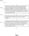
- Fig. 6 is a flowchart schematically illustrating a method 600 of operating the thermal imager 1 when aboard a satellite orbiting Earth, assuming that the thermal imager is arranged such that it faces Earth's surface and the rows of IC chips are oriented in perpendicular to a plane spanned by a flight direction of the satellite and a perpendicular to Earth's surface.
- the method may be performed by the readout circuitry 40, for example.
- the method comprises, at step S610 , setting a sample frequency for capturing readout signals of the array of IC chips such that a field of view, projected on Earth's surface, of a leading row of IC chips at a given sample timing substantially coincides with a field of view, projected on Earth's surface, of an n-th row of IC chips from the first row of IC chips at an n-th sample timing subsequent to the given sample timing, where n is an integer ranging from 2 to N-1, with N the number of rows of IC chips in the array of IC chips.
- This sample frequency f may be calculated as stated above, for example.
- the readout signals of the array of IC chips are captured at a plurality of successive sample timings in accordance with the sample frequency. That is, the successive sample timings may be spaced apart, in time, by 1/f from one another.
- readout signals for one row in the pair of non-adjacent rows of IC chips are compared to corresponding readout signals for the other row in the pair of non-adjacent rows of IC chips (e.g., the third row of IC chips) captured at an m-th sample timing subsequent to the given timing, assuming that the other row in the pair of non-adjacent rows of IC chips is the m-th row of IC chips from the one row in the pair of non-adjacent rows of IC chips, counting all intermediate rows of IC chips.
- the method may comprise comparing the readout signals (thermal image) of any row of IC chips captured at a given sample timing to the readout signals of any other row of IC chips at an appropriately shifted sample timing (i.e., shifted by an integer multiple of 1/f). If the wavelength ranges of (thermal) radiation that can reach the respective rows of IC chips are identical, this enables a stereoscopic analysis. If the wavelength ranges are different, this enables inferring readout signals for the respective field of view projected on ground at new (difference) wavelength ranges, as noted above. Preferably, the readout signals for the outer two rows (i.e., the leading row and the trailing row) are compared to each other.
- thermal imager or satellite described above may correspond to respective method features (of, e.g., a manufacturing method or operating method) that may not be explicitly described, for reasons of conciseness, and vice versa.
- the disclosure of the present document is considered to extend also to such methods and vice versa.
Landscapes
- Engineering & Computer Science (AREA)
- Physics & Mathematics (AREA)
- General Physics & Mathematics (AREA)
- Remote Sensing (AREA)
- Spectroscopy & Molecular Physics (AREA)
- Signal Processing (AREA)
- Multimedia (AREA)
- Aviation & Aerospace Engineering (AREA)
- Toxicology (AREA)
- Health & Medical Sciences (AREA)
- Astronomy & Astrophysics (AREA)
- General Life Sciences & Earth Sciences (AREA)
- Geology (AREA)
- Environmental & Geological Engineering (AREA)
- Life Sciences & Earth Sciences (AREA)
- Photometry And Measurement Of Optical Pulse Characteristics (AREA)
- Radiation Pyrometers (AREA)
- Transforming Light Signals Into Electric Signals (AREA)
- Studio Devices (AREA)
Priority Applications (5)
| Application Number | Priority Date | Filing Date | Title |
|---|---|---|---|
| EP19150221.0A EP3677885B1 (de) | 2019-01-03 | 2019-01-03 | Ungekühlter thermischer bildgeber |
| ES19150221T ES2956789T3 (es) | 2019-01-03 | 2019-01-03 | Cámara térmica no refrigerada |
| PCT/EP2019/086610 WO2020141102A1 (en) | 2019-01-03 | 2019-12-20 | Uncooled thermal imager |
| US17/420,513 US11902697B2 (en) | 2019-01-03 | 2019-12-20 | Uncooled thermal imager |
| US18/437,681 US12192671B2 (en) | 2019-01-03 | 2024-02-09 | Uncooled thermal imager |
Applications Claiming Priority (1)
| Application Number | Priority Date | Filing Date | Title |
|---|---|---|---|
| EP19150221.0A EP3677885B1 (de) | 2019-01-03 | 2019-01-03 | Ungekühlter thermischer bildgeber |
Publications (3)
| Publication Number | Publication Date |
|---|---|
| EP3677885A1 true EP3677885A1 (de) | 2020-07-08 |
| EP3677885B1 EP3677885B1 (de) | 2023-06-21 |
| EP3677885C0 EP3677885C0 (de) | 2023-06-21 |
Family
ID=64959237
Family Applications (1)
| Application Number | Title | Priority Date | Filing Date |
|---|---|---|---|
| EP19150221.0A Active EP3677885B1 (de) | 2019-01-03 | 2019-01-03 | Ungekühlter thermischer bildgeber |
Country Status (4)
| Country | Link |
|---|---|
| US (2) | US11902697B2 (de) |
| EP (1) | EP3677885B1 (de) |
| ES (1) | ES2956789T3 (de) |
| WO (1) | WO2020141102A1 (de) |
Citations (1)
| Publication number | Priority date | Publication date | Assignee | Title |
|---|---|---|---|---|
| US20140211006A1 (en) * | 2012-11-21 | 2014-07-31 | Astrium Sas | Imaging machine with several detector arrays arranged in a focal plane |
Family Cites Families (7)
| Publication number | Priority date | Publication date | Assignee | Title |
|---|---|---|---|---|
| US10057508B2 (en) * | 2013-06-20 | 2018-08-21 | Excelitas Technologies Corp. | Illumination device with integrated thermal imaging sensor |
| US9307156B1 (en) * | 2013-12-19 | 2016-04-05 | Matthew Sinfield | Longwave infrared imaging of a high-temperature, high-intensity light source |
| CN106455974B (zh) * | 2014-06-20 | 2018-12-14 | 拉姆伯斯公司 | 用于有透镜和无透镜的光学感测的系统和方法 |
| US9810581B1 (en) * | 2014-07-28 | 2017-11-07 | MP High Tech Solutions Pty Ltd | Micromechanical device for electromagnetic radiation sensing |
| WO2016037063A1 (en) * | 2014-09-05 | 2016-03-10 | Massachusetts Institute Of Technology | Systems, methods, and apparatus for sensitive thermal imaging |
| WO2017222778A1 (en) * | 2016-06-24 | 2017-12-28 | Flir Systems, Inc. | Thermal-image based video compression systems and methods |
| CN108351254B (zh) * | 2016-09-02 | 2021-10-22 | 索尼半导体解决方案公司 | 摄像装置 |
-
2019
- 2019-01-03 EP EP19150221.0A patent/EP3677885B1/de active Active
- 2019-01-03 ES ES19150221T patent/ES2956789T3/es active Active
- 2019-12-20 US US17/420,513 patent/US11902697B2/en active Active
- 2019-12-20 WO PCT/EP2019/086610 patent/WO2020141102A1/en not_active Ceased
-
2024
- 2024-02-09 US US18/437,681 patent/US12192671B2/en active Active
Patent Citations (1)
| Publication number | Priority date | Publication date | Assignee | Title |
|---|---|---|---|---|
| US20140211006A1 (en) * | 2012-11-21 | 2014-07-31 | Astrium Sas | Imaging machine with several detector arrays arranged in a focal plane |
Non-Patent Citations (5)
| Title |
|---|
| DORIS ANTENSTEINER ET AL: "High-Precision 3D Sensing with Hybrid Light Field & Photometric Stereo Approach in Multi-Line Scan Framework", ELECTRONIC IMAGING, vol. 2017, no. 9, 29 January 2017 (2017-01-29), pages 52 - 60, XP055641605, ISSN: 2470-1173, DOI: 10.2352/ISSN.2470-1173.2017.9.IRIACV-268 * |
| MUELLER J ET AL: "A NOVEL MICROMACHINED 2X128-ELEMENT LINEAR THEMOELECTRIC INFRARED RADIATION SENSOR ARRAY", PROCEEDINGS. MICRO. TEC. VDE WORLD MICROTECHNOLOGIES CONGRESS,PROCEEDINGS OF INTERNATIONAL CONFERENCE ON MICROTECHNOLOGIES, XX, XX, vol. 1, 25 September 2000 (2000-09-25), pages I,465 - 469, XP001189264 * |
| RIENSTRA J ET AL: "Multispectral focal plane assembly for satellite remote sensing", AEROSPACE CONFERENCE, 1998 IEEE SNOWMASS AT ASPEN, CO, USA 21-28 MARCH 1998, NEW YORK, NY, USA,IEEE, US, vol. 5, 21 March 1998 (1998-03-21), pages 233 - 241, XP010287061, ISBN: 978-0-7803-4311-5, DOI: 10.1109/AERO.1998.685824 * |
| ROGALSKI ANTONI ED - CHENNUPATI JAGADISH: "Progress in focal plane array technologies", PROGRESS IN QUANTUM ELECTRONICS, vol. 36, no. 2, May 2012 (2012-05-01), pages 342 - 473, XP028938279, ISSN: 0079-6727, DOI: 10.1016/J.PQUANTELEC.2012.07.001 * |
| WAYNE K. DAVIS: "Conceptual Design And Requirements Of A Pushbroom Focal Plane", PROCEEDINGS OF SPIE, vol. 0282, 29 December 1981 (1981-12-29), pages 29 - 33, XP055641602, ISSN: 0277-786X, DOI: 10.1117/12.931968 * |
Also Published As
| Publication number | Publication date |
|---|---|
| WO2020141102A1 (en) | 2020-07-09 |
| US12192671B2 (en) | 2025-01-07 |
| US11902697B2 (en) | 2024-02-13 |
| ES2956789T3 (es) | 2023-12-28 |
| EP3677885B1 (de) | 2023-06-21 |
| US20220086371A1 (en) | 2022-03-17 |
| US20240187546A1 (en) | 2024-06-06 |
| EP3677885C0 (de) | 2023-06-21 |
Similar Documents
| Publication | Publication Date | Title |
|---|---|---|
| US11108941B2 (en) | Multi-camera imaging systems | |
| Ford et al. | Advanced camera for the Hubble space telescope | |
| US8300108B2 (en) | Multi-channel imaging devices comprising unit cells | |
| Clemens et al. | Mimir: A near-infrared wide-field imager, spectrometer, and polarimeter | |
| US10690479B2 (en) | Optical positioning sensor | |
| US20170227398A1 (en) | Hyperspectral optical element for monolithic detectors | |
| US20200271790A1 (en) | Method and device for detecting incident laser radiation on a spacecraft | |
| Butler et al. | Low-cost uncooled microbolometer imaging system for dual use | |
| US12192671B2 (en) | Uncooled thermal imager | |
| US11378453B2 (en) | Cubesat infrared atmospheric sounder (CIRAS) | |
| JP2014058176A (ja) | 地球センサ及び地球センサを用いた地球エッジ検出方法 | |
| US9360316B2 (en) | System architecture for a constant footprint, constant GSD, constant spatial resolution linescanner | |
| Dave et al. | AWiFS camera for Resourcesat | |
| Diner et al. | WindCam and MSPI: Two cloud and aerosol instrument concepts derived from Terra/MISR heritage | |
| US20250146877A1 (en) | Infrared shack-hartmann wavefront sensor based on cavity-coupled nanoantennas | |
| Malone et al. | Staring MWIR, LWIR and 2-color and scanning LWIR polarimetry technology | |
| Cassidy | Advanced stellar sensors-A new generation | |
| Jeter et al. | Wedge spectrometer concepts for space IR remote sensing | |
| Bounmy et al. | A wide field-of-view low-resolution spectrometer at APEX: instrument design and science forecast | |
| WO1997042765A1 (en) | High resolution and wedge-filter camera system for low earth orbit satellite imaging | |
| Peralta et al. | Recent focal plane arrays for astronomy and remote sensing applications at RVS | |
| Lee et al. | Hyperion: A 0.4 micrometer-2.5 micrometer hyperspectral imager for the NASA Earth Observing-1 mission | |
| Blake | An imaging X-ray spectrometer to study solar activity in conjunction with the SCADM program | |
| Clampin et al. | The Advanced Camera for Surveys | |
| Pavlov et al. | Compact airborne multispectral scanning device |
Legal Events
| Date | Code | Title | Description |
|---|---|---|---|
| PUAI | Public reference made under article 153(3) epc to a published international application that has entered the european phase |
Free format text: ORIGINAL CODE: 0009012 |
|
| STAA | Information on the status of an ep patent application or granted ep patent |
Free format text: STATUS: THE APPLICATION HAS BEEN PUBLISHED |
|
| AK | Designated contracting states |
Kind code of ref document: A1 Designated state(s): AL AT BE BG CH CY CZ DE DK EE ES FI FR GB GR HR HU IE IS IT LI LT LU LV MC MK MT NL NO PL PT RO RS SE SI SK SM TR |
|
| AX | Request for extension of the european patent |
Extension state: BA ME |
|
| STAA | Information on the status of an ep patent application or granted ep patent |
Free format text: STATUS: REQUEST FOR EXAMINATION WAS MADE |
|
| 17P | Request for examination filed |
Effective date: 20210111 |
|
| RBV | Designated contracting states (corrected) |
Designated state(s): AL AT BE BG CH CY CZ DE DK EE ES FI FR GB GR HR HU IE IS IT LI LT LU LV MC MK MT NL NO PL PT RO RS SE SI SK SM TR |
|
| RIC1 | Information provided on ipc code assigned before grant |
Ipc: G01J 5/00 20060101ALI20211029BHEP Ipc: G01J 5/12 20060101ALI20211029BHEP Ipc: H04N 13/204 20180101ALI20211029BHEP Ipc: G01J 5/08 20060101AFI20211029BHEP |
|
| REG | Reference to a national code |
Ref country code: DE Ref legal event code: R079 Free format text: PREVIOUS MAIN CLASS: G01J0005120000 Ref country code: DE Ref legal event code: R079 Ref document number: 602019031225 Country of ref document: DE Free format text: PREVIOUS MAIN CLASS: G01J0005120000 Ipc: G01J0005080600 |
|
| GRAP | Despatch of communication of intention to grant a patent |
Free format text: ORIGINAL CODE: EPIDOSNIGR1 |
|
| STAA | Information on the status of an ep patent application or granted ep patent |
Free format text: STATUS: GRANT OF PATENT IS INTENDED |
|
| RIC1 | Information provided on ipc code assigned before grant |
Ipc: G01J 5/0802 20220101ALI20220208BHEP Ipc: H04N 13/00 20180101ALI20220208BHEP Ipc: H04N 13/218 20180101ALI20220208BHEP Ipc: H04N 5/33 20060101ALI20220208BHEP Ipc: H04N 13/204 20180101ALI20220208BHEP Ipc: G01J 5/00 20060101ALI20220208BHEP Ipc: G01J 5/12 20060101ALI20220208BHEP Ipc: G01J 5/0806 20220101AFI20220208BHEP |
|
| INTG | Intention to grant announced |
Effective date: 20220223 |
|
| GRAJ | Information related to disapproval of communication of intention to grant by the applicant or resumption of examination proceedings by the epo deleted |
Free format text: ORIGINAL CODE: EPIDOSDIGR1 |
|
| STAA | Information on the status of an ep patent application or granted ep patent |
Free format text: STATUS: REQUEST FOR EXAMINATION WAS MADE |
|
| INTC | Intention to grant announced (deleted) | ||
| GRAP | Despatch of communication of intention to grant a patent |
Free format text: ORIGINAL CODE: EPIDOSNIGR1 |
|
| STAA | Information on the status of an ep patent application or granted ep patent |
Free format text: STATUS: GRANT OF PATENT IS INTENDED |
|
| INTG | Intention to grant announced |
Effective date: 20221019 |
|
| GRAS | Grant fee paid |
Free format text: ORIGINAL CODE: EPIDOSNIGR3 |
|
| GRAA | (expected) grant |
Free format text: ORIGINAL CODE: 0009210 |
|
| STAA | Information on the status of an ep patent application or granted ep patent |
Free format text: STATUS: THE PATENT HAS BEEN GRANTED |
|
| RAP3 | Party data changed (applicant data changed or rights of an application transferred) |
Owner name: ORORATECH GMBH |
|
| AK | Designated contracting states |
Kind code of ref document: B1 Designated state(s): AL AT BE BG CH CY CZ DE DK EE ES FI FR GB GR HR HU IE IS IT LI LT LU LV MC MK MT NL NO PL PT RO RS SE SI SK SM TR |
|
| REG | Reference to a national code |
Ref country code: CH Ref legal event code: EP |
|
| REG | Reference to a national code |
Ref country code: DE Ref legal event code: R096 Ref document number: 602019031225 Country of ref document: DE |
|
| P01 | Opt-out of the competence of the unified patent court (upc) registered |
Effective date: 20230601 |
|
| REG | Reference to a national code |
Ref country code: AT Ref legal event code: REF Ref document number: 1581205 Country of ref document: AT Kind code of ref document: T Effective date: 20230715 |
|
| REG | Reference to a national code |
Ref country code: IE Ref legal event code: FG4D |
|
| P04 | Withdrawal of opt-out of the competence of the unified patent court (upc) registered |
Effective date: 20230724 |
|
| U01 | Request for unitary effect filed |
Effective date: 20230721 |
|
| U07 | Unitary effect registered |
Designated state(s): AT BE BG DE DK EE FI FR IT LT LU LV MT NL PT SE SI Effective date: 20230727 |
|
| REG | Reference to a national code |
Ref country code: LT Ref legal event code: MG9D |
|
| PG25 | Lapsed in a contracting state [announced via postgrant information from national office to epo] |
Ref country code: NO Free format text: LAPSE BECAUSE OF FAILURE TO SUBMIT A TRANSLATION OF THE DESCRIPTION OR TO PAY THE FEE WITHIN THE PRESCRIBED TIME-LIMIT Effective date: 20230921 |
|
| PG25 | Lapsed in a contracting state [announced via postgrant information from national office to epo] |
Ref country code: RS Free format text: LAPSE BECAUSE OF FAILURE TO SUBMIT A TRANSLATION OF THE DESCRIPTION OR TO PAY THE FEE WITHIN THE PRESCRIBED TIME-LIMIT Effective date: 20230621 Ref country code: HR Free format text: LAPSE BECAUSE OF FAILURE TO SUBMIT A TRANSLATION OF THE DESCRIPTION OR TO PAY THE FEE WITHIN THE PRESCRIBED TIME-LIMIT Effective date: 20230621 Ref country code: GR Free format text: LAPSE BECAUSE OF FAILURE TO SUBMIT A TRANSLATION OF THE DESCRIPTION OR TO PAY THE FEE WITHIN THE PRESCRIBED TIME-LIMIT Effective date: 20230922 |
|
| REG | Reference to a national code |
Ref country code: ES Ref legal event code: FG2A Ref document number: 2956789 Country of ref document: ES Kind code of ref document: T3 Effective date: 20231228 |
|
| PG25 | Lapsed in a contracting state [announced via postgrant information from national office to epo] |
Ref country code: SK Free format text: LAPSE BECAUSE OF FAILURE TO SUBMIT A TRANSLATION OF THE DESCRIPTION OR TO PAY THE FEE WITHIN THE PRESCRIBED TIME-LIMIT Effective date: 20230621 |
|
| PG25 | Lapsed in a contracting state [announced via postgrant information from national office to epo] |
Ref country code: IS Free format text: LAPSE BECAUSE OF FAILURE TO SUBMIT A TRANSLATION OF THE DESCRIPTION OR TO PAY THE FEE WITHIN THE PRESCRIBED TIME-LIMIT Effective date: 20231021 |
|
| PG25 | Lapsed in a contracting state [announced via postgrant information from national office to epo] |
Ref country code: SM Free format text: LAPSE BECAUSE OF FAILURE TO SUBMIT A TRANSLATION OF THE DESCRIPTION OR TO PAY THE FEE WITHIN THE PRESCRIBED TIME-LIMIT Effective date: 20230621 Ref country code: SK Free format text: LAPSE BECAUSE OF FAILURE TO SUBMIT A TRANSLATION OF THE DESCRIPTION OR TO PAY THE FEE WITHIN THE PRESCRIBED TIME-LIMIT Effective date: 20230621 Ref country code: RO Free format text: LAPSE BECAUSE OF FAILURE TO SUBMIT A TRANSLATION OF THE DESCRIPTION OR TO PAY THE FEE WITHIN THE PRESCRIBED TIME-LIMIT Effective date: 20230621 Ref country code: IS Free format text: LAPSE BECAUSE OF FAILURE TO SUBMIT A TRANSLATION OF THE DESCRIPTION OR TO PAY THE FEE WITHIN THE PRESCRIBED TIME-LIMIT Effective date: 20231021 Ref country code: CZ Free format text: LAPSE BECAUSE OF FAILURE TO SUBMIT A TRANSLATION OF THE DESCRIPTION OR TO PAY THE FEE WITHIN THE PRESCRIBED TIME-LIMIT Effective date: 20230621 |
|
| PG25 | Lapsed in a contracting state [announced via postgrant information from national office to epo] |
Ref country code: PL Free format text: LAPSE BECAUSE OF FAILURE TO SUBMIT A TRANSLATION OF THE DESCRIPTION OR TO PAY THE FEE WITHIN THE PRESCRIBED TIME-LIMIT Effective date: 20230621 |
|
| U20 | Renewal fee for the european patent with unitary effect paid |
Year of fee payment: 6 Effective date: 20240131 |
|
| REG | Reference to a national code |
Ref country code: DE Ref legal event code: R097 Ref document number: 602019031225 Country of ref document: DE |
|
| PLBE | No opposition filed within time limit |
Free format text: ORIGINAL CODE: 0009261 |
|
| STAA | Information on the status of an ep patent application or granted ep patent |
Free format text: STATUS: NO OPPOSITION FILED WITHIN TIME LIMIT |
|
| 26N | No opposition filed |
Effective date: 20240322 |
|
| PG25 | Lapsed in a contracting state [announced via postgrant information from national office to epo] |
Ref country code: MC Free format text: LAPSE BECAUSE OF FAILURE TO SUBMIT A TRANSLATION OF THE DESCRIPTION OR TO PAY THE FEE WITHIN THE PRESCRIBED TIME-LIMIT Effective date: 20230621 |
|
| PG25 | Lapsed in a contracting state [announced via postgrant information from national office to epo] |
Ref country code: MC Free format text: LAPSE BECAUSE OF FAILURE TO SUBMIT A TRANSLATION OF THE DESCRIPTION OR TO PAY THE FEE WITHIN THE PRESCRIBED TIME-LIMIT Effective date: 20230621 |
|
| REG | Reference to a national code |
Ref country code: CH Ref legal event code: PL |
|
| PG25 | Lapsed in a contracting state [announced via postgrant information from national office to epo] |
Ref country code: CH Free format text: LAPSE BECAUSE OF NON-PAYMENT OF DUE FEES Effective date: 20240131 |
|
| PG25 | Lapsed in a contracting state [announced via postgrant information from national office to epo] |
Ref country code: CH Free format text: LAPSE BECAUSE OF NON-PAYMENT OF DUE FEES Effective date: 20240131 |
|
| P05 | Withdrawal of opt-out of the competence of the unified patent court (upc) changed |
Free format text: CASE NUMBER: APP_553706/2023 Effective date: 20230727 |
|
| PG25 | Lapsed in a contracting state [announced via postgrant information from national office to epo] |
Ref country code: IE Free format text: LAPSE BECAUSE OF NON-PAYMENT OF DUE FEES Effective date: 20240103 |
|
| PG25 | Lapsed in a contracting state [announced via postgrant information from national office to epo] |
Ref country code: IE Free format text: LAPSE BECAUSE OF NON-PAYMENT OF DUE FEES Effective date: 20240103 |
|
| U20 | Renewal fee for the european patent with unitary effect paid |
Year of fee payment: 7 Effective date: 20250131 |
|
| PG25 | Lapsed in a contracting state [announced via postgrant information from national office to epo] |
Ref country code: CY Free format text: LAPSE BECAUSE OF FAILURE TO SUBMIT A TRANSLATION OF THE DESCRIPTION OR TO PAY THE FEE WITHIN THE PRESCRIBED TIME-LIMIT; INVALID AB INITIO Effective date: 20190103 |
|
| PG25 | Lapsed in a contracting state [announced via postgrant information from national office to epo] |
Ref country code: HU Free format text: LAPSE BECAUSE OF FAILURE TO SUBMIT A TRANSLATION OF THE DESCRIPTION OR TO PAY THE FEE WITHIN THE PRESCRIBED TIME-LIMIT; INVALID AB INITIO Effective date: 20190103 |
|
| PG25 | Lapsed in a contracting state [announced via postgrant information from national office to epo] |
Ref country code: TR Free format text: LAPSE BECAUSE OF FAILURE TO SUBMIT A TRANSLATION OF THE DESCRIPTION OR TO PAY THE FEE WITHIN THE PRESCRIBED TIME-LIMIT Effective date: 20230621 |
|
| U20 | Renewal fee for the european patent with unitary effect paid |
Year of fee payment: 8 Effective date: 20260202 |
|
| PGFP | Annual fee paid to national office [announced via postgrant information from national office to epo] |
Ref country code: GB Payment date: 20260122 Year of fee payment: 8 |
|
| PGFP | Annual fee paid to national office [announced via postgrant information from national office to epo] |
Ref country code: ES Payment date: 20260217 Year of fee payment: 8 |