EP3677960B1 - Substrat d'affichage, panneau d'affichage et dispositif d'affichage - Google Patents
Substrat d'affichage, panneau d'affichage et dispositif d'affichage Download PDFInfo
- Publication number
- EP3677960B1 EP3677960B1 EP18851831.0A EP18851831A EP3677960B1 EP 3677960 B1 EP3677960 B1 EP 3677960B1 EP 18851831 A EP18851831 A EP 18851831A EP 3677960 B1 EP3677960 B1 EP 3677960B1
- Authority
- EP
- European Patent Office
- Prior art keywords
- slit
- electrode
- groups
- sub
- group
- Prior art date
- Legal status (The legal status is an assumption and is not a legal conclusion. Google has not performed a legal analysis and makes no representation as to the accuracy of the status listed.)
- Active
Links
Images


Classifications
-
- G—PHYSICS
- G02—OPTICS
- G02F—OPTICAL DEVICES OR ARRANGEMENTS FOR THE CONTROL OF LIGHT BY MODIFICATION OF THE OPTICAL PROPERTIES OF THE MEDIA OF THE ELEMENTS INVOLVED THEREIN; NON-LINEAR OPTICS; FREQUENCY-CHANGING OF LIGHT; OPTICAL LOGIC ELEMENTS; OPTICAL ANALOGUE/DIGITAL CONVERTERS
- G02F1/00—Devices or arrangements for the control of the intensity, colour, phase, polarisation or direction of light arriving from an independent light source, e.g. switching, gating or modulating; Non-linear optics
- G02F1/01—Devices or arrangements for the control of the intensity, colour, phase, polarisation or direction of light arriving from an independent light source, e.g. switching, gating or modulating; Non-linear optics for the control of the intensity, phase, polarisation or colour
- G02F1/13—Devices or arrangements for the control of the intensity, colour, phase, polarisation or direction of light arriving from an independent light source, e.g. switching, gating or modulating; Non-linear optics for the control of the intensity, phase, polarisation or colour based on liquid crystals, e.g. single liquid crystal display cells
- G02F1/133—Constructional arrangements; Operation of liquid crystal cells; Circuit arrangements
- G02F1/1333—Constructional arrangements; Manufacturing methods
- G02F1/1337—Surface-induced orientation of the liquid crystal molecules, e.g. by alignment layers
- G02F1/133707—Structures for producing distorted electric fields, e.g. bumps, protrusions, recesses, slits in pixel electrodes
-
- G—PHYSICS
- G02—OPTICS
- G02F—OPTICAL DEVICES OR ARRANGEMENTS FOR THE CONTROL OF LIGHT BY MODIFICATION OF THE OPTICAL PROPERTIES OF THE MEDIA OF THE ELEMENTS INVOLVED THEREIN; NON-LINEAR OPTICS; FREQUENCY-CHANGING OF LIGHT; OPTICAL LOGIC ELEMENTS; OPTICAL ANALOGUE/DIGITAL CONVERTERS
- G02F1/00—Devices or arrangements for the control of the intensity, colour, phase, polarisation or direction of light arriving from an independent light source, e.g. switching, gating or modulating; Non-linear optics
- G02F1/01—Devices or arrangements for the control of the intensity, colour, phase, polarisation or direction of light arriving from an independent light source, e.g. switching, gating or modulating; Non-linear optics for the control of the intensity, phase, polarisation or colour
- G02F1/13—Devices or arrangements for the control of the intensity, colour, phase, polarisation or direction of light arriving from an independent light source, e.g. switching, gating or modulating; Non-linear optics for the control of the intensity, phase, polarisation or colour based on liquid crystals, e.g. single liquid crystal display cells
- G02F1/133—Constructional arrangements; Operation of liquid crystal cells; Circuit arrangements
- G02F1/136—Liquid crystal cells structurally associated with a semi-conducting layer or substrate, e.g. cells forming part of an integrated circuit
- G02F1/1362—Active matrix addressed cells
- G02F1/136286—Wiring, e.g. gate line, drain line
-
- G—PHYSICS
- G02—OPTICS
- G02F—OPTICAL DEVICES OR ARRANGEMENTS FOR THE CONTROL OF LIGHT BY MODIFICATION OF THE OPTICAL PROPERTIES OF THE MEDIA OF THE ELEMENTS INVOLVED THEREIN; NON-LINEAR OPTICS; FREQUENCY-CHANGING OF LIGHT; OPTICAL LOGIC ELEMENTS; OPTICAL ANALOGUE/DIGITAL CONVERTERS
- G02F1/00—Devices or arrangements for the control of the intensity, colour, phase, polarisation or direction of light arriving from an independent light source, e.g. switching, gating or modulating; Non-linear optics
- G02F1/01—Devices or arrangements for the control of the intensity, colour, phase, polarisation or direction of light arriving from an independent light source, e.g. switching, gating or modulating; Non-linear optics for the control of the intensity, phase, polarisation or colour
- G02F1/13—Devices or arrangements for the control of the intensity, colour, phase, polarisation or direction of light arriving from an independent light source, e.g. switching, gating or modulating; Non-linear optics for the control of the intensity, phase, polarisation or colour based on liquid crystals, e.g. single liquid crystal display cells
- G02F1/133—Constructional arrangements; Operation of liquid crystal cells; Circuit arrangements
- G02F1/1333—Constructional arrangements; Manufacturing methods
- G02F1/1337—Surface-induced orientation of the liquid crystal molecules, e.g. by alignment layers
- G02F1/133753—Surface-induced orientation of the liquid crystal molecules, e.g. by alignment layers with different alignment orientations or pretilt angles on a same surface, e.g. for grey scale or improved viewing angle
- G02F1/133757—Surface-induced orientation of the liquid crystal molecules, e.g. by alignment layers with different alignment orientations or pretilt angles on a same surface, e.g. for grey scale or improved viewing angle with different alignment orientations
-
- G—PHYSICS
- G02—OPTICS
- G02F—OPTICAL DEVICES OR ARRANGEMENTS FOR THE CONTROL OF LIGHT BY MODIFICATION OF THE OPTICAL PROPERTIES OF THE MEDIA OF THE ELEMENTS INVOLVED THEREIN; NON-LINEAR OPTICS; FREQUENCY-CHANGING OF LIGHT; OPTICAL LOGIC ELEMENTS; OPTICAL ANALOGUE/DIGITAL CONVERTERS
- G02F1/00—Devices or arrangements for the control of the intensity, colour, phase, polarisation or direction of light arriving from an independent light source, e.g. switching, gating or modulating; Non-linear optics
- G02F1/01—Devices or arrangements for the control of the intensity, colour, phase, polarisation or direction of light arriving from an independent light source, e.g. switching, gating or modulating; Non-linear optics for the control of the intensity, phase, polarisation or colour
- G02F1/13—Devices or arrangements for the control of the intensity, colour, phase, polarisation or direction of light arriving from an independent light source, e.g. switching, gating or modulating; Non-linear optics for the control of the intensity, phase, polarisation or colour based on liquid crystals, e.g. single liquid crystal display cells
- G02F1/133—Constructional arrangements; Operation of liquid crystal cells; Circuit arrangements
- G02F1/1333—Constructional arrangements; Manufacturing methods
- G02F1/1343—Electrodes
- G02F1/134309—Electrodes characterised by their geometrical arrangement
-
- G—PHYSICS
- G02—OPTICS
- G02F—OPTICAL DEVICES OR ARRANGEMENTS FOR THE CONTROL OF LIGHT BY MODIFICATION OF THE OPTICAL PROPERTIES OF THE MEDIA OF THE ELEMENTS INVOLVED THEREIN; NON-LINEAR OPTICS; FREQUENCY-CHANGING OF LIGHT; OPTICAL LOGIC ELEMENTS; OPTICAL ANALOGUE/DIGITAL CONVERTERS
- G02F1/00—Devices or arrangements for the control of the intensity, colour, phase, polarisation or direction of light arriving from an independent light source, e.g. switching, gating or modulating; Non-linear optics
- G02F1/01—Devices or arrangements for the control of the intensity, colour, phase, polarisation or direction of light arriving from an independent light source, e.g. switching, gating or modulating; Non-linear optics for the control of the intensity, phase, polarisation or colour
- G02F1/13—Devices or arrangements for the control of the intensity, colour, phase, polarisation or direction of light arriving from an independent light source, e.g. switching, gating or modulating; Non-linear optics for the control of the intensity, phase, polarisation or colour based on liquid crystals, e.g. single liquid crystal display cells
- G02F1/133—Constructional arrangements; Operation of liquid crystal cells; Circuit arrangements
- G02F1/1333—Constructional arrangements; Manufacturing methods
- G02F1/1343—Electrodes
- G02F1/134309—Electrodes characterised by their geometrical arrangement
- G02F1/134345—Subdivided pixels, e.g. for grey scale or redundancy
-
- G—PHYSICS
- G02—OPTICS
- G02F—OPTICAL DEVICES OR ARRANGEMENTS FOR THE CONTROL OF LIGHT BY MODIFICATION OF THE OPTICAL PROPERTIES OF THE MEDIA OF THE ELEMENTS INVOLVED THEREIN; NON-LINEAR OPTICS; FREQUENCY-CHANGING OF LIGHT; OPTICAL LOGIC ELEMENTS; OPTICAL ANALOGUE/DIGITAL CONVERTERS
- G02F1/00—Devices or arrangements for the control of the intensity, colour, phase, polarisation or direction of light arriving from an independent light source, e.g. switching, gating or modulating; Non-linear optics
- G02F1/01—Devices or arrangements for the control of the intensity, colour, phase, polarisation or direction of light arriving from an independent light source, e.g. switching, gating or modulating; Non-linear optics for the control of the intensity, phase, polarisation or colour
- G02F1/13—Devices or arrangements for the control of the intensity, colour, phase, polarisation or direction of light arriving from an independent light source, e.g. switching, gating or modulating; Non-linear optics for the control of the intensity, phase, polarisation or colour based on liquid crystals, e.g. single liquid crystal display cells
- G02F1/133—Constructional arrangements; Operation of liquid crystal cells; Circuit arrangements
- G02F1/1333—Constructional arrangements; Manufacturing methods
- G02F1/1343—Electrodes
- G02F1/134309—Electrodes characterised by their geometrical arrangement
- G02F1/134372—Electrodes characterised by their geometrical arrangement for fringe field switching [FFS] where the common electrode is not patterned
-
- G—PHYSICS
- G02—OPTICS
- G02F—OPTICAL DEVICES OR ARRANGEMENTS FOR THE CONTROL OF LIGHT BY MODIFICATION OF THE OPTICAL PROPERTIES OF THE MEDIA OF THE ELEMENTS INVOLVED THEREIN; NON-LINEAR OPTICS; FREQUENCY-CHANGING OF LIGHT; OPTICAL LOGIC ELEMENTS; OPTICAL ANALOGUE/DIGITAL CONVERTERS
- G02F1/00—Devices or arrangements for the control of the intensity, colour, phase, polarisation or direction of light arriving from an independent light source, e.g. switching, gating or modulating; Non-linear optics
- G02F1/01—Devices or arrangements for the control of the intensity, colour, phase, polarisation or direction of light arriving from an independent light source, e.g. switching, gating or modulating; Non-linear optics for the control of the intensity, phase, polarisation or colour
- G02F1/13—Devices or arrangements for the control of the intensity, colour, phase, polarisation or direction of light arriving from an independent light source, e.g. switching, gating or modulating; Non-linear optics for the control of the intensity, phase, polarisation or colour based on liquid crystals, e.g. single liquid crystal display cells
- G02F1/133—Constructional arrangements; Operation of liquid crystal cells; Circuit arrangements
- G02F1/136—Liquid crystal cells structurally associated with a semi-conducting layer or substrate, e.g. cells forming part of an integrated circuit
- G02F1/1362—Active matrix addressed cells
- G02F1/13624—Active matrix addressed cells having more than one switching element per pixel
-
- G—PHYSICS
- G02—OPTICS
- G02F—OPTICAL DEVICES OR ARRANGEMENTS FOR THE CONTROL OF LIGHT BY MODIFICATION OF THE OPTICAL PROPERTIES OF THE MEDIA OF THE ELEMENTS INVOLVED THEREIN; NON-LINEAR OPTICS; FREQUENCY-CHANGING OF LIGHT; OPTICAL LOGIC ELEMENTS; OPTICAL ANALOGUE/DIGITAL CONVERTERS
- G02F1/00—Devices or arrangements for the control of the intensity, colour, phase, polarisation or direction of light arriving from an independent light source, e.g. switching, gating or modulating; Non-linear optics
- G02F1/01—Devices or arrangements for the control of the intensity, colour, phase, polarisation or direction of light arriving from an independent light source, e.g. switching, gating or modulating; Non-linear optics for the control of the intensity, phase, polarisation or colour
- G02F1/13—Devices or arrangements for the control of the intensity, colour, phase, polarisation or direction of light arriving from an independent light source, e.g. switching, gating or modulating; Non-linear optics for the control of the intensity, phase, polarisation or colour based on liquid crystals, e.g. single liquid crystal display cells
- G02F1/133—Constructional arrangements; Operation of liquid crystal cells; Circuit arrangements
- G02F1/136—Liquid crystal cells structurally associated with a semi-conducting layer or substrate, e.g. cells forming part of an integrated circuit
- G02F1/1362—Active matrix addressed cells
- G02F1/1368—Active matrix addressed cells in which the switching element is a three-electrode device
-
- G—PHYSICS
- G02—OPTICS
- G02F—OPTICAL DEVICES OR ARRANGEMENTS FOR THE CONTROL OF LIGHT BY MODIFICATION OF THE OPTICAL PROPERTIES OF THE MEDIA OF THE ELEMENTS INVOLVED THEREIN; NON-LINEAR OPTICS; FREQUENCY-CHANGING OF LIGHT; OPTICAL LOGIC ELEMENTS; OPTICAL ANALOGUE/DIGITAL CONVERTERS
- G02F2203/00—Function characteristic
- G02F2203/30—Gray scale
Definitions
- This disclosure relates to the field of display technologies, and particularly to a display substrate, a display panel, and a display device.
- TFT-LCD Thin Film Transistor Liquid Crystal Display
- Chinese patent application CN105629607A discloses an array substrate that includes: a plurality of pixels including sub-pixels forming a matrix, each sub-pixel including a pair of sub-pixel portions; a plurality of data lines; a plurality of gate lines intersecting with the plurality of data lines; and a plurality of pairs of transistors configured to control the plurality of pairs of sub-pixel portions; wherein: each pair of transistors are disposed adjacent to an intersection between a gate line and a data line, across at least one of the gate line or the data line, and are configured to control a pair of sub-pixel portions in neighboring rows or columns of sub-pixel portions.
- US patent US9723769B2 discloses an alignment film including a first pre-tilt functional group, a second pre-tilt functional group and a first vertical alignment functional group, which are linked to polysiloxane on a substrate.
- the first vertical alignment functional group includes a cyclic compound and is aligned substantially perpendicularly to the substrate.
- the first pre-tilt functional group is cross-linked to the second pre-tilt functional group and tilted with respect to the substrate.
- Korean patent KR101296621B1 discloses to apply the IPS mode to the R, G, and B sub-pixels among the R, G, B, and W pixels and applies the FFS mode, which is known to have a higher aperture ratio than the IPS mode, to the W sub-pixels, so that the conventional IPS mode is achieved. It relates to a liquid crystal display device and a method for manufacturing the same, which improve transmission characteristics and lower Clc and Cst values compared to the case of designing in the conventional FFS mode, thereby making it advantageous for large panel applications.
- This liquid crystal display device discloses gate lines and data lines that vertically cross on the substrate to define R, G, B, W sub-pixels; a thin film transistor disposed at an intersection of the gate line and the data line; a common wiring parallel to the gate wiring; a common electrode and a first pixel electrode formed in the R, G, and B sub-pixels and parallel to each other to form a transverse electric field; a counter electrode formed in a plate shape in the W sub-pixel and a second pixel electrode insulated from the counter electrode and having a plurality of slits; and a counter substrate facing the substrate and a liquid crystal layer interposed between the substrate and the counter substrate, wherein the R, G, and B sub-pixels are transversely formed by the common electrode and the first pixel electrode formed on the same layer. It is driven by an electric field, and the W sub-pixel is driven by a fringe electric field by the counter electrode and the second pixel electrode insulated from each other.
- the claimed invention provides a display substrate for a fringe field switching (FS) mode liquid crystal display according to claim 1.
- FFS fringe field switching
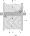
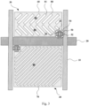
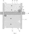
- a display substrate includes: a base substrate, a plurality of pixel units arranged in an array on the base substrate, data lines 10 located between any two adjacent columns of pixel units, and a group of gate lines 20 arranged corresponding to respective rows of pixel units; where each gate line 20 segments a pixel region of each pixel unit in a corresponding row of pixel units into a first sub-pixel region 30 and a second sub-pixel region 40; each pixel unit includes slit electrodes, and two thin film transistors 50 arranged corresponding respectively to the first sub-pixel region 30 and the second sub-pixel region 40 and the slit electrodes include a first slit electrode 60 and a second slit electrode 70 corresponding respectively to the first sub-pixel region 30 and the second sub-pixel region 40.
- each slit group 80 includes a plurality of slits 81 extended in a same direction
- an extension direction of each slit in one of the at least one slit group 80 of the first slit electrode 60 is different from an extension direction of each slit in at least one of the at least one slit group 80 of the second slit electrode 70
- a direction of a corresponding electric field formed by the one of the at least one slit group of the first slit electrode is different from a direction of a corresponding electric field formed by the at least one of the at least one slit group of the second slit electrode.
- the display substrate further includes plate-shaped electrodes arranged spaced from the slit electrodes in direction of and proximate to the base substrate.
- the plate-shaped electrodes are particularly a common electrode (not illustrated)
- the slit electrodes are particularly pixel electrodes
- the first slit electrode 60 is insulated from the second slit electrode 70.
- the plate-shaped electrodes can be pixel electrodes
- the slit electrodes can be a common electrode.
- a line width of each gate line 20 can range from 2 ⁇ m to 30 ⁇ m, and a line width of each data line 10 can range from 2 ⁇ m to 10 ⁇ m.
- the two thin film transistors 50 control the first sub-pixel region 30 and the second sub-pixel region 40 respectively, where driving voltage of the first sub-pixel region 30 and the second sub-pixel region 40 can be adjusted respectively according to areas of the two sub-pixel regions, so that liquid crystal molecules corresponding to the two sub-pixel regions at a liquid crystal layer can be deflected in different directions to thereby compensate effectively for a color cast arising from only one deflection direction of the liquid crystal molecules; and the first slit electrode 60 and the second slit electrode 70 of each pixel unit include at least one slit group 80 respectively, and the extension direction of each slit in one of the at least one slit group 80 of the first slit electrode 60 is different from the extension direction of each slit in at least one of the at least one slit group 80 of the second slit electrode 70, so that each of the first sub-pixel region 30 and the second sub-pixel region 40 includes at least one domain, and deflection directions of corresponding liquid
- each thin film transistor 50 includes a gate 51, a gate insulation layer (not illustrated) formed above the gate 51, an active layer 53 formed above the gate insulation layer, and a source 52 and a drain 53 connected respectively with the active layer 54.
- gates 51 of the two thin film transistors 50 of each pixel unit arranged corresponding respectively to the first sub-pixel region 30 and the second sub-pixel region 40 are connected respectively with a gate line 20 corresponding to the pixel unit
- sources 52 of the two thin film transistors 50 are connected respectively with two data lines located on two sides of the pixel unit
- drains 53 of the two thin film transistors 50 are connected respectively with the first slit electrode 60 and the second slit electrode 70.
- slit line widths of respective slits 81 are the same, and the spacing between any two adjacent slits 81 arranged in the same direction is the same; and the same applies to the second slit electrode 70.
- Each slit 81 of the first slit electrode 60 has the same first slit line width, and any two adjacent slits 81 arranged in the same direction of the first slit electrode 60 have the same first slit spacing; and each slit 81 of the second slit electrode 70 has the same second slit line width, and any two adjacent slits 81 arranged in the same direction of the second slit electrode 70 has the same second slit spacing.
- liquid crystal molecules in the same domain have substantially the same deflection direction, and are arranged uniformly and regularly in order.
- values of the first slit line width, the first slit spacing, the second slit line width, and the second slit spacing will not be limited, and in some embodiments, all of the first slit line width, the first slit spacing, the second slit line width, and the second slit spacing can range from 2 ⁇ m to 10 ⁇ m.
- an area of the first sub-pixel region 30 is not equal to an area of the second sub-pixel region 40, so that it is convenient for the two thin film transistors 50 to provide different driving voltage according to the different areas of the first sub-pixel region 30 and the second sub-pixel region 40 respectively, therefore deflection directions of liquid crystal molecules corresponding to the two sub-pixel regions at the liquid crystal layer will be different to thereby further alleviate the color cast of the display device.
- design parameters of the two thin film transistors 50 can be changed to provide the two thin film transistors 50 with different channel width to length ratios so as to provide the first sub-pixel region 30 and the second sub-pixel region 40 with different voltage as needed.
- the first sub-pixel region and the second sub-pixel region are provided with different driving voltage by their corresponding thin film transistors according to their different areas so that there is a better display effect of the sub-pixel region with the smaller area, at a low grayscale.
- the area of the first sub-pixel region is larger than the area of the second sub-pixel region, the first slit line width is less than the second slit line width, and the first slit spacing is less than the second slit spacing.
- the area of the first sub-pixel region is smaller than the area of the second sub-pixel region, the first slit line width is greater than the second slit line width, and the first slit spacing is greater than the second slit spacing.
- the slit line width and the slit spacing of a slit electrode corresponding to a sub-pixel region with the smaller area are larger than the slit line width and the slit spacing of a slit electrode corresponding to a sub-pixel region with the larger area respectively, so that for the sub-pixel region with the smaller area, the larger slit line width and the larger slit spacing increase an area of the slit electrode to emit lines of electric forces, i.e., enhance a valid area of the slit electrode, so that the light transmittance of the sub-pixel region with the smaller area can be improved effectively, which will enable the two sub-pixel regions with different areas to receive approximate intensities of light to thereby further alleviate the color cast of the display device, and facilitate a uniform angle of view of the display device.
- the voltage difference between adjacent grayscales in a low-grayscale area is less than the voltage difference between adjacent grayscales in a high-grayscale area, so the valid area of the slit electrode in the sub-pixel region with the smaller area can be increased to thereby improve the valid light transmittance thereof so as to improve the resolution of the display device displaying at a low grayscale.
- the first slit line width is no less than 1/n of the second slit line width
- the first slit spacing is no less than 1/n of the second slit spacing, where n is a positive integer.
- each of the first slit electrode 60 and the second slit electrode 70 includes one slit group 80, and an angle between an extension direction of each slit in the one slit group 80 of the first slit electrode 60, and an extension direction of each slit in the one slit group 80 of the second slit electrode 70 ranges from 30° to 150°.
- each pixel unit includes two domains.
- the angle between the extension direction of each slit in the one slit group 80 of the first slit electrode 60, and the extension direction of each slit in the one slit group 80 of the second slit electrode 70 is 90° ⁇ 1°.
- the first slit electrode 60 includes one slit group 80
- the second slit electrode 70 includes two slit groups 80 with different slit extension directions, and an angle between extension directions of slits in the two slit groups 80 of the second slit electrode 70 ranges from 10° to 170°; and in order to further alleviate the color cast of the display device, the two slit groups 80 of the second slit electrode 70 are arranged in an extension direction of the data lines 10, and an angle between an extension direction of each slit in a slit group 80, in the second slit electrode 70, arranged proximate to a corresponding gate line 20, and an extension direction of each slit in the one slit group 80 of the first slit electrode 60 ranges from 30° to 150°.
- the second slit electrode 70 includes one slit group 80
- the first slit electrode 60 includes two slit groups 80 with different extension directions of slits, and an angle between extension directions of slits in the two slit groups 80 of the first slit electrode 60 ranges from 10° to 170°
- the two slit groups 80 of the first slit electrode 60 are arranged in an extension direction of the data lines 10, and an angle between an extension direction of each slit in a slit group 80, in the first slit electrode 60, arranged proximate to a corresponding gate line 20, and an extension direction of each slit in the one slit group 80 of the second slit electrode 70 ranges from 30° to 150°.
- one sub-pixel region includes two domains, and the other sub-pixel region includes one domain, that is, each pixel unit includes three domains, thus resulting in a larger angle of view of the display device.
- each of the first slit electrode 60 and the second slit electrode 70 includes two slit groups 80 with different slit extension directions, an angle between extension directions of slits in the two slit groups 80 of the first slit electrode 60 ranges from 10° to 170°, and an angle between extension directions of slits in the two slit groups 80 of the second slit electrode 70 ranges from 10° to 170°; and in order to further alleviate the color cast of the display device, the two slit groups 80 of the first slit electrode 60, and the two slit groups 80 of the second slit electrode 70 are arranged in the extension direction of the data lines 10 respectively, and an angle between an extension direction of each slit in a slit group 80, in the first slit electrode 60, arranged proximate to a corresponding gate line 20, and an extension direction of each slit in a slit group 80, in the second slit electrode 70, arranged prox
- each of the first slit electrode 60 and the second slit electrode 70 includes four slit groups 80 arranged in two rows and two columns, a row arrangement direction of the four slit groups 80 of the first slit electrode 60 is parallel to the gate lines 20, a column arrangement direction of the four slit groups 80 of the first slit electrode 60 is parallel to the data lines 10, a row arrangement direction of the four slit groups 80 of the second slit electrode 70 is parallel to the gate lines 20, and a column arrangement direction of the four slit groups 80 of the second slit electrode 70 is parallel to the data lines 10; and furthermore, an angle between extension directions of slits in any two adjacent slit groups 80 in the first slit electrode ranges from 10° to 170°, and an angle between extension directions of slits in any two adjacent slit groups 80 in the second slit electrode ranges from 10° to 170°.
- angles between extension directions of slits in two pairs of slit groups 80, in the first slit electrode 60 and the second slit electrode 70, arranged proximate to a corresponding gate line 20, and positioned opposite to each other range from 30° to 150° respectively, so that each pixel unit includes eight domains, thus resulting in a larger angle of view of the display device.
- the embodiments of the invention further provide a display panel including the display substrate according to any one of the technical solutions above.
- a color cast of a display device to which the display panel is applied can be alleviated to thereby improve the display effect of the display device.
- the embodiments of the invention further provide a display device including the display panel according to the technical solution above.
- a color cast of the display device can be alleviated to thereby greatly improve the display effect of the display device.
- the types of the display device are not limited, and can be a flat panel display, a tablet computer, a mobile phone, or a vehicle-mounted display, etc.
Landscapes
- Physics & Mathematics (AREA)
- Nonlinear Science (AREA)
- Mathematical Physics (AREA)
- Chemical & Material Sciences (AREA)
- Crystallography & Structural Chemistry (AREA)
- General Physics & Mathematics (AREA)
- Optics & Photonics (AREA)
- Engineering & Computer Science (AREA)
- Microelectronics & Electronic Packaging (AREA)
- Geometry (AREA)
- Spectroscopy & Molecular Physics (AREA)
- Liquid Crystal (AREA)
Claims (12)
- Un substrat d'affichage pour un afficheur à cristaux liquides à mode de commutation de champ marginal, FFS, comprenant :un substrat de base ;une pluralité d'unités de pixels agencées en réseau sur le substrat de base ;des lignes de données (10) situées entre deux colonnes adjacentes quelconques d'unités de pixels ; etun groupe de lignes de grille (20) agencées en correspondance avec des rangées respectives d'unités de pixels ;chaque ligne de grille (20) segmente une zone de pixels de chaque unité de pixels dans une rangée correspondante d'unités de pixels en une première zone de sous-pixels (30) et une deuxième zone de sous-pixels (40) ; chaque unité de pixel comprend des électrodes à fente (60, 70) et deux transistors à couches minces (50) agencés en correspondance respectivement avec la première zone de sous-pixel (30) et la deuxième zone de sous-pixel (40) ; les électrodes à fente (60, 70) comprennent une première électrode à fentes (60) et une deuxième électrode à fentes (70) correspondant respectivement à la première zone de sous-pixel (30) et à la deuxième zone de sous-pixel (40), avec :chacune parmi la première électrode à fentes (60) et la deuxième électrode à fentes (70) comprend au moins un groupe de fentes (80), chaque groupe de fentes (80) comprend une pluralité de fentes (81) agencées dans une même direction, une direction d'extension de chaque fente (81) dans l'un desdits groupes de fentes (80) de la première électrode à fentes (60) est différente d'une direction d'extension de chaque fente (81) dans au moins un desdits groupes de fentes (80) de la deuxième électrode à fentes (70) ;le substrat d'affichage comprenant en outre des électrodes en forme de plaque agencées entre une couche dans laquelle se trouvent les électrodes à fente (60, 70) et le substrat de base ; une direction d'un champ électrique formé entre ledit un groupe dudit au moins un groupe de fentes (80) de la première électrode à fentes (60) et les électrodes en forme de plaque est différente d'une direction d'un champ électrique formé entre ledit un groupe dudit au moins un groupe de fentes (80) de la deuxième électrode à fentes (70) et les électrodes en forme de plaque ;chaque fente (81) de la première électrode à fentes (60) ayant une même première largeur de ligne de fente, et deux fentes adjacentes quelconques (81), agencées dans la même direction, de la première électrode à fentes (60) ayant un même premier espacement de fentes ; etchaque fente (81) de la deuxième électrode à fentes (70) ayant une même deuxième largeur de ligne de fente, et deux fentes adjacentes quelconques (81), agencées dans la même direction, de la deuxième électrode à fentes (70) ayant un même deuxième espacement de fentes ;caractérisé en ce que,une superficie de la première zone de sous-pixel (30) est plus grande qu'une superficie de la deuxième zone de sous-pixel (40), la première largeur de ligne de fente est inférieure à la deuxième largeur de ligne de fente, et le premier espacement de fentes est inférieur au deuxième espacement des fentes ; ouune zone de la première zone de sous-pixel (30) est plus petite qu'une zone de la deuxième zone de sous-pixel (40), la première largeur de ligne de fente est supérieure à la deuxième largeur de ligne de fente, et le premier espacement de fentes est supérieur au deuxième espacement de fentes.
- Le substrat d'affichage selon la revendication 1, dans lequel les électrodes en forme de plaque sont agencées à distance des électrodes à fente (60, 70) dans la direction et à proximité du substrat de base.
- Le substrat d'affichage selon la revendication 1, dans lequel lorsque la superficie de la première zone de sous-pixel (30) est n fois la superficie de la deuxième zone de sous-pixel (40), la première largeur de ligne de fente n'est pas inférieure à 1/n de la deuxième largeur de ligne de fente, et le premier espacement de fentes n'est pas inférieur à 1/n de la deuxième largeur de ligne de fente, n étant un nombre positif.
- Le substrat d'affichage selon la revendication 1, dans lequel chacune parmi la première électrode à fentes (60) et la deuxième électrode à fentes (70) comprend un groupe de fentes (80), et un angle entre une direction d'extension de chaque fente (81) dans ledit un groupe de fentes (80) de la première électrode à fentes (60), et une direction d'extension de chaque fente (81) dans ledit un groupe de fentes (80) de la deuxième électrode à fentes (70) est compris entre 30° et 150°.
- Le substrat d'affichage selon la revendication 1, dans lequel la première électrode à fentes (60) comprend un groupe de fentes (80), la deuxième électrode à fentes (70) comprend deux groupes de fentes (80) comprenant des fentes (81) dans des directions d'extension différentes, et un angle entre les directions d'extension des fentes (81) dans les deux groupes de fentes (80) de la deuxième électrode à fentes (70) est compris entre 10° et 170° ; ou
la deuxième électrode à fentes (70) comprend un groupe de fentes (80), la première électrode à fentes (60) comprend deux groupes de fentes (80) comprenant des fentes (81) dans des directions d'extension différentes, et un angle entre les directions d'extension des fentes (81) dans les deux groupes de fentes (80) de la première électrode à fentes (60) est compris entre 10° et 170°. - Le substrat d'affichage selon la revendication 5, dans lequel lorsque la deuxième électrode à fentes (70) comprend deux groupes de fentes (80) comprenant des fentes (81) dans des directions d'extension différentes, les deux groupes de fentes (80) de la deuxième électrode à fentes (70) sont agencés dans une direction d'extension des lignes de données (10), et un angle entre une direction d'extension de chaque fente (81) dans un groupe de fentes (80), dans la deuxième électrode à fentes (70), agencée à proximité d'une ligne de grille (20) correspondante, et une direction d'extension de chaque fente (81) dans ledit un groupe de fentes (80) de la première électrode à fentes (60) est compris entre 30° et 150° ; ou
lorsque la première électrode à fentes (60) comprend deux groupes de fentes (80) comprenant des fentes (81) dans des directions d'extension différentes, les deux groupes de fentes (80) de la deuxième électrode à fentes (70) sont agencés dans une direction d'extension des lignes de données (10), et un angle entre une direction d'extension de chaque fente (81) dans un groupe de fentes (80), dans la première électrode à fentes (60), agencée à proximité d'une ligne de grille (20) correspondante, et une direction d'extension de chaque fente (81) dans ledit un groupe de fentes (80) de la deuxième électrode à fentes (70) est compris entre 30° et 150°. - Le substrat d'affichage selon la revendication 1, dans lequel chacune parmi la première électrode à fentes (60) et la deuxième électrode à fentes (70) comprend deux groupes de fentes (80) comprenant des fentes (81) dans des directions d'extension différentes, un angle entre les directions d'extension des fentes (81) dans les deux groupes de fentes (80) de la première électrode à fentes (60) est compris entre 10° et 170°, et un angle entre les directions d'extension des fentes (81) dans les deux groupes de fentes (80) de la deuxième électrode à fentes (70) est compris entre 10° et 170°.
- Le substrat d'affichage selon la revendication 7, dans lequel les deux groupes de fentes (80) de la première électrode à fentes (60) et les deux groupes de fentes (80) de la deuxième électrode à fentes (70) sont agencés dans une direction d'extension des lignes de données (10), respectivement, et un angle entre une direction d'extension de chaque fente (81) dans un groupe de fentes (80), dans la première électrode à fentes (60), agencée à proximité d'une ligne de grille (20) correspondante, et une direction d'extension de chaque fente (81) dans un groupe de fentes (80), dans la deuxième électrode à fentes (70), agencée à proximité de la ligne de grille correspondante (20), est compris entre 30° et 150°.
- Le substrat d'affichage selon la revendication 1, dans lequel chacune parmi la première électrode à fentes (60) et la deuxième électrode à fentes (70) comprend quatre groupes de fentes (80) agencés en deux rangées et deux colonnes, une direction d'agencement de rangées et une direction d'agencement de colonnes des quatre groupes de fentes (80) de la première électrode à fentes (60) sont parallèles aux lignes de grille (20) et aux lignes de données (10) respectivement, et une direction d'agencement de rangées et une direction d'agencement de colonnes des quatre fentes des groupes (80) de la deuxième électrode à fentes (70) sont parallèles aux lignes de grille (20) et aux lignes de données (10) respectivement ; et un angle entre les directions d'extension des fentes (81) dans deux groupes de fentes adjacents quelconques (80) dans la première électrode à fentes (60) est compris entre 10° et 170°, et un angle entre les directions d'extension de fentes (81) dans deux groupes de fentes adjacents quelconques (80) dans la deuxième électrode à fentes (70) est compris entre 10° et 170°.
- Le substrat d'affichage selon la revendication 9, dans lequel les angles entre les directions d'extension des fentes (81) dans deux paires de groupes de fentes (80), dans la première électrode à fentes (60) et la deuxième électrode à fentes (70), agencées à proximité de une ligne de grille (20) correspondante, et positionnées l'une en face de l'autre, sont compris entre 30° et 150° respectivement.
- Un panneau d'affichage, comprenant le substrat d'affichage selon l'une quelconque des revendications 1 à 10.
- Un dispositif d'affichage, comprenant le panneau d'affichage selon la revendication 11.
Priority Applications (1)
| Application Number | Priority Date | Filing Date | Title |
|---|---|---|---|
| EP23191627.1A EP4254395A3 (fr) | 2017-08-28 | 2018-03-28 | Substrat d'affichage, panneau d'affichage et dispositif d'affichage |
Applications Claiming Priority (2)
| Application Number | Priority Date | Filing Date | Title |
|---|---|---|---|
| CN201710751655.6A CN107463040B (zh) | 2017-08-28 | 2017-08-28 | 一种显示基板、显示面板及显示装置 |
| PCT/CN2018/080963 WO2019041801A1 (fr) | 2017-08-28 | 2018-03-28 | Substrat d'affichage, panneau d'affichage et dispositif d'affichage |
Related Child Applications (2)
| Application Number | Title | Priority Date | Filing Date |
|---|---|---|---|
| EP23191627.1A Division EP4254395A3 (fr) | 2017-08-28 | 2018-03-28 | Substrat d'affichage, panneau d'affichage et dispositif d'affichage |
| EP23191627.1A Division-Into EP4254395A3 (fr) | 2017-08-28 | 2018-03-28 | Substrat d'affichage, panneau d'affichage et dispositif d'affichage |
Publications (3)
| Publication Number | Publication Date |
|---|---|
| EP3677960A1 EP3677960A1 (fr) | 2020-07-08 |
| EP3677960A4 EP3677960A4 (fr) | 2021-06-02 |
| EP3677960B1 true EP3677960B1 (fr) | 2023-11-15 |
Family
ID=60549359
Family Applications (2)
| Application Number | Title | Priority Date | Filing Date |
|---|---|---|---|
| EP23191627.1A Pending EP4254395A3 (fr) | 2017-08-28 | 2018-03-28 | Substrat d'affichage, panneau d'affichage et dispositif d'affichage |
| EP18851831.0A Active EP3677960B1 (fr) | 2017-08-28 | 2018-03-28 | Substrat d'affichage, panneau d'affichage et dispositif d'affichage |
Family Applications Before (1)
| Application Number | Title | Priority Date | Filing Date |
|---|---|---|---|
| EP23191627.1A Pending EP4254395A3 (fr) | 2017-08-28 | 2018-03-28 | Substrat d'affichage, panneau d'affichage et dispositif d'affichage |
Country Status (4)
| Country | Link |
|---|---|
| US (1) | US20210278731A1 (fr) |
| EP (2) | EP4254395A3 (fr) |
| CN (1) | CN107463040B (fr) |
| WO (1) | WO2019041801A1 (fr) |
Families Citing this family (13)
| Publication number | Priority date | Publication date | Assignee | Title |
|---|---|---|---|---|
| CN107463040B (zh) * | 2017-08-28 | 2020-11-10 | 京东方科技集团股份有限公司 | 一种显示基板、显示面板及显示装置 |
| CN107895568A (zh) | 2017-12-28 | 2018-04-10 | 深圳市华星光电技术有限公司 | 液晶显示装置 |
| CN108732806A (zh) * | 2018-05-29 | 2018-11-02 | 上海天马微电子有限公司 | 显示面板、显示装置和显示面板的制造方法 |
| CN108983510B (zh) * | 2018-08-02 | 2022-03-29 | 上海天马微电子有限公司 | 显示面板和3d打印系统 |
| CN111929952B (zh) * | 2019-05-13 | 2023-12-01 | 瀚宇彩晶股份有限公司 | 显示面板 |
| CN113767328B (zh) * | 2020-04-03 | 2023-10-17 | 京东方科技集团股份有限公司 | 显示基板、显示面板和显示装置 |
| CN114078397B (zh) * | 2020-08-21 | 2024-11-05 | 群创光电股份有限公司 | 显示面板以及显示装置 |
| CN112596315B (zh) * | 2020-12-15 | 2022-09-09 | 京东方科技集团股份有限公司 | 阵列基板及其制备方法、显示装置 |
| CN115704973A (zh) * | 2021-08-09 | 2023-02-17 | 瀚宇彩晶股份有限公司 | 显示装置以及其驱动方法 |
| CN114296280B (zh) * | 2021-12-23 | 2024-01-26 | 绵阳惠科光电科技有限公司 | 显示面板及交通工具 |
| US12223921B2 (en) | 2022-01-10 | 2025-02-11 | Wuhan Boe Optoelectronics Technology Co., Ltd. | Drive method for controlling data voltage of display panel, and display apparatus including source drive circuit for controlling data voltage of display panel |
| CN114660856B (zh) * | 2022-03-16 | 2024-02-20 | Tcl华星光电技术有限公司 | 阵列基板及显示装置 |
| CN115268151B (zh) * | 2022-08-22 | 2023-10-13 | 京东方科技集团股份有限公司 | 像素结构及其制备方法、显示面板 |
Family Cites Families (11)
| Publication number | Priority date | Publication date | Assignee | Title |
|---|---|---|---|---|
| KR101296621B1 (ko) * | 2005-12-29 | 2013-08-14 | 엘지디스플레이 주식회사 | 액정표시소자 및 그 제조방법 |
| KR101481690B1 (ko) * | 2008-07-23 | 2015-01-12 | 삼성디스플레이 주식회사 | 표시기판, 이의 제조방법 및 이를 갖는 표시장치 |
| TWI415100B (zh) * | 2010-12-30 | 2013-11-11 | Au Optronics Corp | 可補償饋通電壓之液晶顯示面板 |
| KR101820966B1 (ko) * | 2011-10-20 | 2018-01-23 | 삼성디스플레이 주식회사 | 액정표시장치, 배향막 및 이들을 제조하는 방법들 |
| TWI514058B (zh) * | 2011-11-11 | 2015-12-21 | Au Optronics Corp | 畫素陣列 |
| CN202383394U (zh) * | 2011-11-22 | 2012-08-15 | 北京京东方光电科技有限公司 | 一种阵列基板 |
| TWI476492B (zh) * | 2012-10-11 | 2015-03-11 | Innocom Tech Shenzhen Co Ltd | 畫素電極結構及使用其之顯示面板 |
| CN104614904A (zh) * | 2015-03-11 | 2015-05-13 | 京东方科技集团股份有限公司 | 一种像素结构及其驱动方法、阵列基板和显示装置 |
| TWI564641B (zh) * | 2015-05-22 | 2017-01-01 | 友達光電股份有限公司 | 畫素結構及具有此畫素結構的畫素陣列 |
| CN105629607A (zh) * | 2016-01-14 | 2016-06-01 | 京东方科技集团股份有限公司 | 一种阵列基板、显示面板和显示装置 |
| CN107463040B (zh) * | 2017-08-28 | 2020-11-10 | 京东方科技集团股份有限公司 | 一种显示基板、显示面板及显示装置 |
-
2017
- 2017-08-28 CN CN201710751655.6A patent/CN107463040B/zh active Active
-
2018
- 2018-03-28 EP EP23191627.1A patent/EP4254395A3/fr active Pending
- 2018-03-28 WO PCT/CN2018/080963 patent/WO2019041801A1/fr not_active Ceased
- 2018-03-28 EP EP18851831.0A patent/EP3677960B1/fr active Active
- 2018-03-28 US US16/329,396 patent/US20210278731A1/en not_active Abandoned
Also Published As
| Publication number | Publication date |
|---|---|
| CN107463040A (zh) | 2017-12-12 |
| EP4254395A3 (fr) | 2024-01-03 |
| EP3677960A1 (fr) | 2020-07-08 |
| WO2019041801A1 (fr) | 2019-03-07 |
| US20210278731A1 (en) | 2021-09-09 |
| EP3677960A4 (fr) | 2021-06-02 |
| EP4254395A2 (fr) | 2023-10-04 |
| CN107463040B (zh) | 2020-11-10 |
Similar Documents
| Publication | Publication Date | Title |
|---|---|---|
| EP4254395A2 (fr) | Substrat d'affichage, panneau d'affichage et dispositif d'affichage | |
| US9858870B2 (en) | Pixel unit, pixel array and liquid crystal display panel | |
| CN109634012B (zh) | 显示面板 | |
| KR101931699B1 (ko) | 액정 표시 장치 | |
| KR101518329B1 (ko) | 액정 표시 장치 | |
| KR101663565B1 (ko) | 액정표시장치 | |
| US8817212B2 (en) | Liquid crystal display panel | |
| US9429805B2 (en) | Array substrate, display panel and display device | |
| KR102094741B1 (ko) | 액정 표시 장치 | |
| US20180031928A1 (en) | Array substrate, driving method thereof, and display panel | |
| US20120154724A1 (en) | Array substrate and liquid crystal display device | |
| KR20040098728A (ko) | 수평 전계 인가형 액정 표시 패널 | |
| CN107589602A (zh) | 一种具有新型像素设计的液晶显示面板 | |
| KR20140021749A (ko) | 액정 표시 장치 | |
| US20210366947A1 (en) | Array substrate and display device | |
| KR20130139548A (ko) | 액정 표시 장치 | |
| US20190331967A1 (en) | Pixle structure and array substrate | |
| JP2016139070A (ja) | 表示装置 | |
| KR20150047963A (ko) | 액정 표시 장치 | |
| US10303002B2 (en) | Pixel structure, driving method thereof, display substrate and display device | |
| US10014323B2 (en) | Array substrate, curved display panel and curved display device | |
| CN110531558B (zh) | 阵列基板、液晶显示面板及显示装置 | |
| KR20070070722A (ko) | 액정표시장치 | |
| US20170017128A1 (en) | Liquid crystal display having improved pixel electrode shapes | |
| US9558697B2 (en) | Display device driving sub-pixels of a plurality of colors |
Legal Events
| Date | Code | Title | Description |
|---|---|---|---|
| STAA | Information on the status of an ep patent application or granted ep patent |
Free format text: STATUS: THE INTERNATIONAL PUBLICATION HAS BEEN MADE |
|
| PUAI | Public reference made under article 153(3) epc to a published international application that has entered the european phase |
Free format text: ORIGINAL CODE: 0009012 |
|
| STAA | Information on the status of an ep patent application or granted ep patent |
Free format text: STATUS: REQUEST FOR EXAMINATION WAS MADE |
|
| 17P | Request for examination filed |
Effective date: 20190522 |
|
| AK | Designated contracting states |
Kind code of ref document: A1 Designated state(s): AL AT BE BG CH CY CZ DE DK EE ES FI FR GB GR HR HU IE IS IT LI LT LU LV MC MK MT NL NO PL PT RO RS SE SI SK SM TR |
|
| AX | Request for extension of the european patent |
Extension state: BA ME |
|
| DAV | Request for validation of the european patent (deleted) | ||
| DAX | Request for extension of the european patent (deleted) | ||
| A4 | Supplementary search report drawn up and despatched |
Effective date: 20210430 |
|
| RIC1 | Information provided on ipc code assigned before grant |
Ipc: G02F 1/1343 20060101AFI20210423BHEP Ipc: G02F 1/1337 20060101ALI20210423BHEP Ipc: G02F 1/1362 20060101ALI20210423BHEP Ipc: G09G 3/20 20060101ALI20210423BHEP Ipc: G09G 3/36 20060101ALI20210423BHEP |
|
| GRAP | Despatch of communication of intention to grant a patent |
Free format text: ORIGINAL CODE: EPIDOSNIGR1 |
|
| STAA | Information on the status of an ep patent application or granted ep patent |
Free format text: STATUS: GRANT OF PATENT IS INTENDED |
|
| INTG | Intention to grant announced |
Effective date: 20230612 |
|
| P01 | Opt-out of the competence of the unified patent court (upc) registered |
Effective date: 20230527 |
|
| GRAS | Grant fee paid |
Free format text: ORIGINAL CODE: EPIDOSNIGR3 |
|
| GRAA | (expected) grant |
Free format text: ORIGINAL CODE: 0009210 |
|
| STAA | Information on the status of an ep patent application or granted ep patent |
Free format text: STATUS: THE PATENT HAS BEEN GRANTED |
|
| AK | Designated contracting states |
Kind code of ref document: B1 Designated state(s): AL AT BE BG CH CY CZ DE DK EE ES FI FR GB GR HR HU IE IS IT LI LT LU LV MC MK MT NL NO PL PT RO RS SE SI SK SM TR |
|
| REG | Reference to a national code |
Ref country code: CH Ref legal event code: EP Ref country code: GB Ref legal event code: FG4D |
|
| REG | Reference to a national code |
Ref country code: DE Ref legal event code: R096 Ref document number: 602018061248 Country of ref document: DE |
|
| REG | Reference to a national code |
Ref country code: IE Ref legal event code: FG4D |
|
| REG | Reference to a national code |
Ref country code: LT Ref legal event code: MG9D |
|
| REG | Reference to a national code |
Ref country code: NL Ref legal event code: MP Effective date: 20231115 |
|
| PG25 | Lapsed in a contracting state [announced via postgrant information from national office to epo] |
Ref country code: GR Free format text: LAPSE BECAUSE OF FAILURE TO SUBMIT A TRANSLATION OF THE DESCRIPTION OR TO PAY THE FEE WITHIN THE PRESCRIBED TIME-LIMIT Effective date: 20240216 |
|
| PG25 | Lapsed in a contracting state [announced via postgrant information from national office to epo] |
Ref country code: IS Free format text: LAPSE BECAUSE OF FAILURE TO SUBMIT A TRANSLATION OF THE DESCRIPTION OR TO PAY THE FEE WITHIN THE PRESCRIBED TIME-LIMIT Effective date: 20240315 |
|
| PG25 | Lapsed in a contracting state [announced via postgrant information from national office to epo] |
Ref country code: LT Free format text: LAPSE BECAUSE OF FAILURE TO SUBMIT A TRANSLATION OF THE DESCRIPTION OR TO PAY THE FEE WITHIN THE PRESCRIBED TIME-LIMIT Effective date: 20231115 |
|
| REG | Reference to a national code |
Ref country code: AT Ref legal event code: MK05 Ref document number: 1632312 Country of ref document: AT Kind code of ref document: T Effective date: 20231115 |
|
| PG25 | Lapsed in a contracting state [announced via postgrant information from national office to epo] |
Ref country code: NL Free format text: LAPSE BECAUSE OF FAILURE TO SUBMIT A TRANSLATION OF THE DESCRIPTION OR TO PAY THE FEE WITHIN THE PRESCRIBED TIME-LIMIT Effective date: 20231115 |
|
| PG25 | Lapsed in a contracting state [announced via postgrant information from national office to epo] |
Ref country code: AT Free format text: LAPSE BECAUSE OF FAILURE TO SUBMIT A TRANSLATION OF THE DESCRIPTION OR TO PAY THE FEE WITHIN THE PRESCRIBED TIME-LIMIT Effective date: 20231115 |
|
| PG25 | Lapsed in a contracting state [announced via postgrant information from national office to epo] |
Ref country code: ES Free format text: LAPSE BECAUSE OF FAILURE TO SUBMIT A TRANSLATION OF THE DESCRIPTION OR TO PAY THE FEE WITHIN THE PRESCRIBED TIME-LIMIT Effective date: 20231115 |
|
| PG25 | Lapsed in a contracting state [announced via postgrant information from national office to epo] |
Ref country code: NL Free format text: LAPSE BECAUSE OF FAILURE TO SUBMIT A TRANSLATION OF THE DESCRIPTION OR TO PAY THE FEE WITHIN THE PRESCRIBED TIME-LIMIT Effective date: 20231115 Ref country code: LT Free format text: LAPSE BECAUSE OF FAILURE TO SUBMIT A TRANSLATION OF THE DESCRIPTION OR TO PAY THE FEE WITHIN THE PRESCRIBED TIME-LIMIT Effective date: 20231115 Ref country code: IS Free format text: LAPSE BECAUSE OF FAILURE TO SUBMIT A TRANSLATION OF THE DESCRIPTION OR TO PAY THE FEE WITHIN THE PRESCRIBED TIME-LIMIT Effective date: 20240315 Ref country code: GR Free format text: LAPSE BECAUSE OF FAILURE TO SUBMIT A TRANSLATION OF THE DESCRIPTION OR TO PAY THE FEE WITHIN THE PRESCRIBED TIME-LIMIT Effective date: 20240216 Ref country code: ES Free format text: LAPSE BECAUSE OF FAILURE TO SUBMIT A TRANSLATION OF THE DESCRIPTION OR TO PAY THE FEE WITHIN THE PRESCRIBED TIME-LIMIT Effective date: 20231115 Ref country code: BG Free format text: LAPSE BECAUSE OF FAILURE TO SUBMIT A TRANSLATION OF THE DESCRIPTION OR TO PAY THE FEE WITHIN THE PRESCRIBED TIME-LIMIT Effective date: 20240215 Ref country code: AT Free format text: LAPSE BECAUSE OF FAILURE TO SUBMIT A TRANSLATION OF THE DESCRIPTION OR TO PAY THE FEE WITHIN THE PRESCRIBED TIME-LIMIT Effective date: 20231115 Ref country code: PT Free format text: LAPSE BECAUSE OF FAILURE TO SUBMIT A TRANSLATION OF THE DESCRIPTION OR TO PAY THE FEE WITHIN THE PRESCRIBED TIME-LIMIT Effective date: 20240315 |
|
| PG25 | Lapsed in a contracting state [announced via postgrant information from national office to epo] |
Ref country code: SE Free format text: LAPSE BECAUSE OF FAILURE TO SUBMIT A TRANSLATION OF THE DESCRIPTION OR TO PAY THE FEE WITHIN THE PRESCRIBED TIME-LIMIT Effective date: 20231115 Ref country code: RS Free format text: LAPSE BECAUSE OF FAILURE TO SUBMIT A TRANSLATION OF THE DESCRIPTION OR TO PAY THE FEE WITHIN THE PRESCRIBED TIME-LIMIT Effective date: 20231115 Ref country code: PL Free format text: LAPSE BECAUSE OF FAILURE TO SUBMIT A TRANSLATION OF THE DESCRIPTION OR TO PAY THE FEE WITHIN THE PRESCRIBED TIME-LIMIT Effective date: 20231115 Ref country code: NO Free format text: LAPSE BECAUSE OF FAILURE TO SUBMIT A TRANSLATION OF THE DESCRIPTION OR TO PAY THE FEE WITHIN THE PRESCRIBED TIME-LIMIT Effective date: 20240215 Ref country code: LV Free format text: LAPSE BECAUSE OF FAILURE TO SUBMIT A TRANSLATION OF THE DESCRIPTION OR TO PAY THE FEE WITHIN THE PRESCRIBED TIME-LIMIT Effective date: 20231115 Ref country code: HR Free format text: LAPSE BECAUSE OF FAILURE TO SUBMIT A TRANSLATION OF THE DESCRIPTION OR TO PAY THE FEE WITHIN THE PRESCRIBED TIME-LIMIT Effective date: 20231115 |
|
| PG25 | Lapsed in a contracting state [announced via postgrant information from national office to epo] |
Ref country code: DK Free format text: LAPSE BECAUSE OF FAILURE TO SUBMIT A TRANSLATION OF THE DESCRIPTION OR TO PAY THE FEE WITHIN THE PRESCRIBED TIME-LIMIT Effective date: 20231115 |
|
| PG25 | Lapsed in a contracting state [announced via postgrant information from national office to epo] |
Ref country code: CZ Free format text: LAPSE BECAUSE OF FAILURE TO SUBMIT A TRANSLATION OF THE DESCRIPTION OR TO PAY THE FEE WITHIN THE PRESCRIBED TIME-LIMIT Effective date: 20231115 |
|
| PG25 | Lapsed in a contracting state [announced via postgrant information from national office to epo] |
Ref country code: SK Free format text: LAPSE BECAUSE OF FAILURE TO SUBMIT A TRANSLATION OF THE DESCRIPTION OR TO PAY THE FEE WITHIN THE PRESCRIBED TIME-LIMIT Effective date: 20231115 |
|
| PG25 | Lapsed in a contracting state [announced via postgrant information from national office to epo] |
Ref country code: SM Free format text: LAPSE BECAUSE OF FAILURE TO SUBMIT A TRANSLATION OF THE DESCRIPTION OR TO PAY THE FEE WITHIN THE PRESCRIBED TIME-LIMIT Effective date: 20231115 Ref country code: SK Free format text: LAPSE BECAUSE OF FAILURE TO SUBMIT A TRANSLATION OF THE DESCRIPTION OR TO PAY THE FEE WITHIN THE PRESCRIBED TIME-LIMIT Effective date: 20231115 Ref country code: RO Free format text: LAPSE BECAUSE OF FAILURE TO SUBMIT A TRANSLATION OF THE DESCRIPTION OR TO PAY THE FEE WITHIN THE PRESCRIBED TIME-LIMIT Effective date: 20231115 Ref country code: IT Free format text: LAPSE BECAUSE OF FAILURE TO SUBMIT A TRANSLATION OF THE DESCRIPTION OR TO PAY THE FEE WITHIN THE PRESCRIBED TIME-LIMIT Effective date: 20231115 Ref country code: EE Free format text: LAPSE BECAUSE OF FAILURE TO SUBMIT A TRANSLATION OF THE DESCRIPTION OR TO PAY THE FEE WITHIN THE PRESCRIBED TIME-LIMIT Effective date: 20231115 Ref country code: DK Free format text: LAPSE BECAUSE OF FAILURE TO SUBMIT A TRANSLATION OF THE DESCRIPTION OR TO PAY THE FEE WITHIN THE PRESCRIBED TIME-LIMIT Effective date: 20231115 Ref country code: CZ Free format text: LAPSE BECAUSE OF FAILURE TO SUBMIT A TRANSLATION OF THE DESCRIPTION OR TO PAY THE FEE WITHIN THE PRESCRIBED TIME-LIMIT Effective date: 20231115 |
|
| REG | Reference to a national code |
Ref country code: DE Ref legal event code: R097 Ref document number: 602018061248 Country of ref document: DE |
|
| PLBE | No opposition filed within time limit |
Free format text: ORIGINAL CODE: 0009261 |
|
| STAA | Information on the status of an ep patent application or granted ep patent |
Free format text: STATUS: NO OPPOSITION FILED WITHIN TIME LIMIT |
|
| 26N | No opposition filed |
Effective date: 20240819 |
|
| PG25 | Lapsed in a contracting state [announced via postgrant information from national office to epo] |
Ref country code: SI Free format text: LAPSE BECAUSE OF FAILURE TO SUBMIT A TRANSLATION OF THE DESCRIPTION OR TO PAY THE FEE WITHIN THE PRESCRIBED TIME-LIMIT Effective date: 20231115 |
|
| PG25 | Lapsed in a contracting state [announced via postgrant information from national office to epo] |
Ref country code: SI Free format text: LAPSE BECAUSE OF FAILURE TO SUBMIT A TRANSLATION OF THE DESCRIPTION OR TO PAY THE FEE WITHIN THE PRESCRIBED TIME-LIMIT Effective date: 20231115 |
|
| REG | Reference to a national code |
Ref country code: CH Ref legal event code: PL |
|
| PG25 | Lapsed in a contracting state [announced via postgrant information from national office to epo] |
Ref country code: LU Free format text: LAPSE BECAUSE OF NON-PAYMENT OF DUE FEES Effective date: 20240328 |
|
| PG25 | Lapsed in a contracting state [announced via postgrant information from national office to epo] |
Ref country code: MC Free format text: LAPSE BECAUSE OF FAILURE TO SUBMIT A TRANSLATION OF THE DESCRIPTION OR TO PAY THE FEE WITHIN THE PRESCRIBED TIME-LIMIT Effective date: 20231115 |
|
| PG25 | Lapsed in a contracting state [announced via postgrant information from national office to epo] |
Ref country code: MC Free format text: LAPSE BECAUSE OF FAILURE TO SUBMIT A TRANSLATION OF THE DESCRIPTION OR TO PAY THE FEE WITHIN THE PRESCRIBED TIME-LIMIT Effective date: 20231115 Ref country code: LU Free format text: LAPSE BECAUSE OF NON-PAYMENT OF DUE FEES Effective date: 20240328 |
|
| REG | Reference to a national code |
Ref country code: BE Ref legal event code: MM Effective date: 20240331 |
|
| PG25 | Lapsed in a contracting state [announced via postgrant information from national office to epo] |
Ref country code: BE Free format text: LAPSE BECAUSE OF NON-PAYMENT OF DUE FEES Effective date: 20240331 |
|
| PG25 | Lapsed in a contracting state [announced via postgrant information from national office to epo] |
Ref country code: FR Free format text: LAPSE BECAUSE OF NON-PAYMENT OF DUE FEES Effective date: 20240331 |
|
| PG25 | Lapsed in a contracting state [announced via postgrant information from national office to epo] |
Ref country code: IE Free format text: LAPSE BECAUSE OF NON-PAYMENT OF DUE FEES Effective date: 20240328 |
|
| PG25 | Lapsed in a contracting state [announced via postgrant information from national office to epo] |
Ref country code: IE Free format text: LAPSE BECAUSE OF NON-PAYMENT OF DUE FEES Effective date: 20240328 Ref country code: FR Free format text: LAPSE BECAUSE OF NON-PAYMENT OF DUE FEES Effective date: 20240331 Ref country code: BE Free format text: LAPSE BECAUSE OF NON-PAYMENT OF DUE FEES Effective date: 20240331 Ref country code: CH Free format text: LAPSE BECAUSE OF NON-PAYMENT OF DUE FEES Effective date: 20240331 |
|
| PG25 | Lapsed in a contracting state [announced via postgrant information from national office to epo] |
Ref country code: CY Free format text: LAPSE BECAUSE OF FAILURE TO SUBMIT A TRANSLATION OF THE DESCRIPTION OR TO PAY THE FEE WITHIN THE PRESCRIBED TIME-LIMIT; INVALID AB INITIO Effective date: 20180328 |
|
| PG25 | Lapsed in a contracting state [announced via postgrant information from national office to epo] |
Ref country code: HU Free format text: LAPSE BECAUSE OF FAILURE TO SUBMIT A TRANSLATION OF THE DESCRIPTION OR TO PAY THE FEE WITHIN THE PRESCRIBED TIME-LIMIT; INVALID AB INITIO Effective date: 20180328 |
|
| PG25 | Lapsed in a contracting state [announced via postgrant information from national office to epo] |
Ref country code: FI Free format text: LAPSE BECAUSE OF FAILURE TO SUBMIT A TRANSLATION OF THE DESCRIPTION OR TO PAY THE FEE WITHIN THE PRESCRIBED TIME-LIMIT Effective date: 20231115 |
|
| PG25 | Lapsed in a contracting state [announced via postgrant information from national office to epo] |
Ref country code: TR Free format text: LAPSE BECAUSE OF FAILURE TO SUBMIT A TRANSLATION OF THE DESCRIPTION OR TO PAY THE FEE WITHIN THE PRESCRIBED TIME-LIMIT Effective date: 20231115 |
|
| PGFP | Annual fee paid to national office [announced via postgrant information from national office to epo] |
Ref country code: GB Payment date: 20260324 Year of fee payment: 9 |
|
| PGFP | Annual fee paid to national office [announced via postgrant information from national office to epo] |
Ref country code: DE Payment date: 20260319 Year of fee payment: 9 |