EP3677982B1 - Générateur de tension de référence - Google Patents
Générateur de tension de référence Download PDFInfo
- Publication number
- EP3677982B1 EP3677982B1 EP19217070.2A EP19217070A EP3677982B1 EP 3677982 B1 EP3677982 B1 EP 3677982B1 EP 19217070 A EP19217070 A EP 19217070A EP 3677982 B1 EP3677982 B1 EP 3677982B1
- Authority
- EP
- European Patent Office
- Prior art keywords
- capacitor
- operational amplifier
- reference voltage
- node
- switch
- Prior art date
- Legal status (The legal status is an assumption and is not a legal conclusion. Google has not performed a legal analysis and makes no representation as to the accuracy of the status listed.)
- Active
Links
Images


Classifications
-
- G—PHYSICS
- G05—CONTROLLING; REGULATING
- G05F—SYSTEMS FOR REGULATING ELECTRIC OR MAGNETIC VARIABLES
- G05F1/00—Automatic systems in which deviations of an electric quantity from one or more predetermined values are detected at the output of the system and fed back to a device within the system to restore the detected quantity to its predetermined value or values, i.e. retroactive systems
- G05F1/10—Regulating voltage or current
- G05F1/46—Regulating voltage or current wherein the variable actually regulated by the final control device is DC
- G05F1/56—Regulating voltage or current wherein the variable actually regulated by the final control device is DC using semiconductor devices in series with the load as final control devices
-
- G—PHYSICS
- G05—CONTROLLING; REGULATING
- G05F—SYSTEMS FOR REGULATING ELECTRIC OR MAGNETIC VARIABLES
- G05F3/00—Non-retroactive systems for regulating electric variables by using an uncontrolled element, or an uncontrolled combination of elements, such element or such combination having self-regulating properties
- G05F3/02—Regulating voltage or current
- G05F3/08—Regulating voltage or current wherein the variable is DC
- G05F3/10—Regulating voltage or current wherein the variable is DC using uncontrolled devices with non-linear characteristics
- G05F3/16—Regulating voltage or current wherein the variable is DC using uncontrolled devices with non-linear characteristics being semiconductor devices
- G05F3/20—Regulating voltage or current wherein the variable is DC using uncontrolled devices with non-linear characteristics being semiconductor devices using diode- transistor combinations
- G05F3/30—Regulators using the difference between the base-emitter voltages of two bipolar transistors operating at different current densities
-
- G—PHYSICS
- G05—CONTROLLING; REGULATING
- G05F—SYSTEMS FOR REGULATING ELECTRIC OR MAGNETIC VARIABLES
- G05F1/00—Automatic systems in which deviations of an electric quantity from one or more predetermined values are detected at the output of the system and fed back to a device within the system to restore the detected quantity to its predetermined value or values, i.e. retroactive systems
- G05F1/10—Regulating voltage or current
- G05F1/46—Regulating voltage or current wherein the variable actually regulated by the final control device is DC
- G05F1/56—Regulating voltage or current wherein the variable actually regulated by the final control device is DC using semiconductor devices in series with the load as final control devices
- G05F1/575—Regulating voltage or current wherein the variable actually regulated by the final control device is DC using semiconductor devices in series with the load as final control devices characterised by the feedback circuit
-
- H—ELECTRICITY
- H03—ELECTRONIC CIRCUITRY
- H03F—AMPLIFIERS
- H03F3/00—Amplifiers with only discharge tubes or only semiconductor devices as amplifying elements
- H03F3/45—Differential amplifiers
- H03F3/45071—Differential amplifiers with semiconductor devices only
-
- H—ELECTRICITY
- H03—ELECTRONIC CIRCUITRY
- H03F—AMPLIFIERS
- H03F2200/00—Indexing scheme relating to amplifiers
- H03F2200/129—Indexing scheme relating to amplifiers there being a feedback over the complete amplifier
-
- H—ELECTRICITY
- H03—ELECTRONIC CIRCUITRY
- H03F—AMPLIFIERS
- H03F2200/00—Indexing scheme relating to amplifiers
- H03F2200/156—One or more switches are realised in the feedback circuit of the amplifier stage
-
- H—ELECTRICITY
- H03—ELECTRONIC CIRCUITRY
- H03F—AMPLIFIERS
- H03F2203/00—Indexing scheme relating to amplifiers with only discharge tubes or only semiconductor devices as amplifying elements covered by H03F3/00
- H03F2203/45—Indexing scheme relating to differential amplifiers
- H03F2203/45116—Feedback coupled to the input of the differential amplifier
-
- H—ELECTRICITY
- H03—ELECTRONIC CIRCUITRY
- H03F—AMPLIFIERS
- H03F2203/00—Indexing scheme relating to amplifiers with only discharge tubes or only semiconductor devices as amplifying elements covered by H03F3/00
- H03F2203/45—Indexing scheme relating to differential amplifiers
- H03F2203/45512—Indexing scheme relating to differential amplifiers the FBC comprising one or more capacitors, not being switched capacitors, and being coupled between the LC and the IC
-
- H—ELECTRICITY
- H03—ELECTRONIC CIRCUITRY
- H03F—AMPLIFIERS
- H03F2203/00—Indexing scheme relating to amplifiers with only discharge tubes or only semiconductor devices as amplifying elements covered by H03F3/00
- H03F2203/45—Indexing scheme relating to differential amplifiers
- H03F2203/45514—Indexing scheme relating to differential amplifiers the FBC comprising one or more switched capacitors, and being coupled between the LC and the IC
Definitions
- a conventional reference voltage generator is a circuit that produces a substantially constant output reference voltage. Such circuit can be used for any number of reasons such as generation of a power supply voltage, measurements with respect to a threshold value, etc.
- a conventional bandgap voltage reference generator is a temperature independent voltage reference circuit widely used in integrated circuits. During operation, the conventional bandgap voltage reference generator produces a fixed output voltage regardless of power supply variations, temperature changes, and circuit loading from a device.
- a conventional bandgap reference voltage generator commonly has an output voltage around 1.25 VDC.
- Conventional bandgap reference voltage generators can include any number of active or passive circuit components such as resistors, capacitors, inductors, transformers, operational-amplifiers, etc., to generate a respective output voltage.
- the input offset voltage is a parameter defining the differential DC voltage required between the inputs (inverting and non-inverting inputs) of an amplifier to control the output of the amplifier to zero volts. If left uncorrected, the input offset voltage of a respective operational amplifier may result in undesirable errors in the corresponding reference output voltage, resulting in overall poor circuit performance.
- US 6 819 163 B1 discloses a switched capacitor voltage reference circuit that includes a transconductance circuit that receives an output signal from an amplifier and outputs a current that depends on its input voltage.
- the circuit further includes a charge pump that is controlled by the amplifier output.
- the transconductance circuit provides a reference voltage at the output terminal of the switched capacitor generation circuit.
- a capacitor capacitively couples the output terminal of the switched capacitor circuit to the inverting terminal of the amplifier during the generation phase.
- US 5 945 871 A discloses a reference voltage generator that includes an amplifier, a first capacitor that is configured to be selectively coupled between an output and an inverting input of the amplifier, and a second capacitor that is configured to be selectively coupled between an output and a non-inverting input of the amplifier.
- embodiments herein include novel ways of providing improved generation of a constant or substantially fixed reference voltage.
- the reference voltage generator includes: an amplifier; a capacitor network including one or more capacitors; and a switch control circuit to control connectivity of the capacitor network with respect to the amplifier input/output.
- the switch control circuit controls connectivity of a first capacitor (of the capacitor network) in and out of a feedback path of the amplifier to produce a substantially constant reference voltage.
- the reference voltage generator as described herein is operable to provide input offset voltage correction of the amplifier via repeatedly switching between: i) a first mode in which the first capacitor is absent from the feedback path of the amplifier such as during charging of the first capacitor, and ii) a second mode of inserting the charged first capacitor into the feedback path of the amplifier.
- the reference voltage generator and corresponding components take the form of circuitry.
- such resources/components can be instantiated in any suitable manner.
- the switch control circuit While in the first mode, the switch control circuit is operable to configure the amplifier in a unity gain mode in which an output of the amplifier is coupled to an inverting input of the amplifier. While in the second mode, the switch control circuit is operable to configure the amplifier to operate in a gain mode in which the first capacitor is coupled in the feedback path such as between the inverting input of the amplifier and the output of the amplifier.
- the reference voltage generator as described herein includes a first semiconductor device and a first current driver.
- the reference voltage generator circuit also includes a second semiconductor device and a second current driver.
- the switch control circuit is operable to couple the first current driver to the first semiconductor device.
- the first current driver supplies (or drives) first current through a first semiconductor device during the first mode to generate a first voltage that is inputted to a non-inverting input of the amplifier;
- a second current driver supplies (or drives) second current through the second semiconductor device during the first mode to generate a second voltage that is used at least in part to charge the first capacitor.
- the amplifier is operated in a unity gain mode during the first mode.
- the switch control circuit While operating in the second mode, the switch control circuit is operable to couple the second current driver to the first semiconductor device.
- the first current driver is potentially deactivated and/or disconnected from the first semiconductor device.
- the second current driver supplies the second current through the first semiconductor device to generate a third voltage that is inputted to non-inverting input of the amplifier.
- the first capacitor is connected between the output of the amplifier and the inverting input of the amplifier.
- the first semiconductor device and the second semiconductor device can be of the same type (such as a bipolar junction transistor or other suitable component); an area factor associated with the first semiconductor device and the second semiconductor device can be substantially equal such that the devices are matched in type and size.
- the first current driver output is operable to output a first substantially constant current during the first mode and the second mode. Recall that during the first mode, the first current driver outputs current to the first semiconductor device; during the second mode, the first current driver outputs current to the second semiconductor device.
- the second current driver output is operable to output a second constant or substantially fixed current during the first mode.
- the fixed current outputted from the first driver in both the first and second mode is substantially greater than the fixed current outputted by the second driver circuit (in the first mode).
- the reference voltage generator further includes a biasing circuit operable to switch between driving the first current driver and the second current driver based on a first bias signal and a second bias signal.
- the first bias signal is used to initialize (start or ramp up) operation of the reference voltage generator to produce the reference voltage; the second bias signal is applied after initialization and varies depending on a magnitude of the reference voltage generated by the amplifier.
- a magnitude of the reference voltage is substantially constant over a range of temperature.
- the magnitude of the reference voltage is less than 1 VDC (Volts DC).
- the magnitude of the reference voltage can be any suitable value.
- the network of capacitors further includes a second capacitor, and a third capacitor.
- Each of the first capacitor, the second capacitor, and the third capacitor is coupled to an inverting input of the amplifier.
- the switch control circuit connects the first capacitor and the second capacitor in parallel; during the second mode when the first capacitor is inserted in the feedback path, the second capacitor and the third capacitor are connected in parallel.
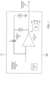
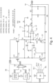
- FIG. 1 is an example diagram illustrating implementation of a reference voltage generator.
- the reference voltage generator 100 (such as an electronic device, circuit, etc.) includes an amplifier 140, current source 121, capacitor C1, switch controller 145, and switches S1 and S2.
- a first node of the capacitor C1 is coupled to the inverting input of the amplifier 140.
- the second node of the capacitor C1 is coupled to switches S1 and S2.
- switch S1 selectively couples the capacitor C1 to the output 141 of amplifier 140; switch S2 selectively couples the capacitor C1 to a ground reference voltage.
- switch controller 145 produces control signals 105 (such as control signal 105-1 and control signal 105-2) to control a state of respective switches S1 and S2.
- Current source 121 outputs current to charge the capacitor C1 depending on a current phase of a repetitive control cycle in which the reference voltage generator 100 is operated.
- Amplifier 140 produces reference voltage 150.
- the switch controller 145 controls connectivity of capacitor C1 (such as one capacitor of multiple capacitors in a capacitor network) in and out of a feedback path 115 (such as between the output 141 of the amplifier 140 and the inverting input node (-)) of the amplifier 140 to produce a substantially constant reference voltage 150.
- capacitor C1 such as one capacitor of multiple capacitors in a capacitor network
- the switch controller 145 of the reference voltage generator 100 is operable to provide input offset voltage correction of the amplifier 140 via repeatedly switching between: i) a first mode in which the capacitor C1 is absent or removed from the feedback path 115 of the amplifier 140 during charging of the capacitor C1, and ii) a second mode of inserting the capacitor C1 into the feedback path 115 of the amplifier 140.
- the switch controller 145 produces the control signal 105-1 such that switch S1 is open; the switch controller 145 produces the control signal 105-2 such that switch S2 is closed.
- the switch controller 145 produces the control signal 105-1 such that switch S1 is closed; the switch controller 145 produces the control signal 105-2 such that switch S2 is open.
- opening of a respective switch means that the respective switch (such as S1 or S2) provides an open circuit or high impedance path; closing of a respective switch means that the respective switch provides a closed circuit path or low impedance path.
- the reference voltage generator 100 and corresponding components take the form of circuitry.
- such components and circuitry can be instantiated in any suitable manner.
- the reference voltage generator 100 is a so-called bandgap reference voltage generator; although, the reference voltage generator 100 can be any suitable type of electronic device operable to produce a respective reference voltage 150.
- a magnitude of the reference voltage 150 generated by the amplifier 140 is substantially constant over a range of temperature.
- the magnitude of the reference voltage 150 generated by the reference voltage generator 100 is less than 1 VDC (Volts DC).
- parameters of the reference voltage generator 100 can be adjusted such that the magnitude of the reference voltage 150 is any desired value (greater than or less than 1 VDC).
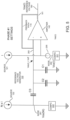
- FIG. 2A is an example diagram illustrating an implementation of a reference voltage generator according to embodiments herein.
- the example reference voltage generator 100 includes a bias circuit 265, switch controller 145, amplifier 140, current source 121, current source 122, component 221 (such as a first semiconductor device), component 222 (such as a second semiconductor device), capacitor C1, capacitor C2, and capacitor C3.
- a value of capacitor C3 is selected (such as fixed value) for the reference voltage generator 100.
- Embodiments herein further include selecting a value of capacitor C2 to adjust a temperature coefficient (to provide first order temperature compensation) of generating the reference voltage 150 across a range of different temperature values.
- a magnitude of capacitor C3 is chosen to control a magnitude of the reference voltage 150.
- bias circuit 265 of the reference voltage generator 100 includes bias resource 210, bias resource 220, and multiplexer 230.
- Switch controller 145 of the reference voltage generator 100 produces control signals 105-1, 105-1A, 105-2, PS, and SEL.
- the reference voltage generator 100 further includes switches S1, S2, S3, S4, S5, S6, S7, S8, and S9.
- the switch controller 145 controls the state of the respective switches between a first operational phase and a second operational phase.
- the switch controller 145 generally generates the controls signal 105-1 and control signal 105-1A to be a logic high when the control signal 105-2 is a logic low. Conversely, the switch controller 145 generates the controls signal 105-1 to be a logic low when the control signal 105-2 is a logic high.
- Control signal 105-1 generated by the switch controller 145 controls a state of switches S3, S4, S6 and S8.
- Control signal 105-1A generated by the switch controller 145 controls a state of switch S2.
- Control signal 105-2 (such as an inverse of control signal 105-1) generated by the switch controller 145 controls a state of switches S1, S5, and S7.
- Control signal PS controls a state of sampling switch S9. Different states of controlling the switches and corresponding reference voltage 150 in different phases is further discussed below in FIGS. 3-7 . Note that there is a dead time between transitions associated with control signals 105-1 and 105-2.
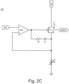
- FIG. 2B is an example diagram illustrating a constant gm bias circuit according to embodiments herein.
- the bias circuit 210 includes amplifier OA2, transistors M1, M2, M3, and M4. Bias circuit 210 receives input voltage Vdd and produces bias voltage PBIAS0.
- the transistor M2 is 4 times the size of transistor M1.
- FIG. 2C is an example diagram illustrating bias circuit according to embodiments herein.
- the bias circuit 220 includes amplifier OA3, transistor M5, resistor R5, resistor Rz, and capacitor Cc. Resistor Rz and capacitor Cc are present for stability in circuit 220. Bias circuit 220 receives input voltage Vref and produces bias voltage PBIAS 1.
- the transistor M5 is fabricated with substantially the same parameters (size, shape, type, etc.) as current driver 121 and 122.
- Amplifier OA3 operates in a balanced state in which the voltage of the inverting input equals a voltage of the non-inverting input.
- the bias circuit generates control signal PBIAS1.
- the output circuit 268 of the reference voltage generator 100 includes switch S9, capacitor C5, resistor RF1, and capacitor CF1.
- the switch controller 145 controls switch S9 (ON and OFF at appropriate times via signal PS) to sample the output voltage (Vo) of the amplifier 140 and output it through the low pass filter (combination of resistor RF1 and capacitor CF1) to generate the reference voltage 150.
- the multiplexer 230 switches between i) connecting the output PBIAS0 of bias resource 210 to the current drivers 121 and 122, and ii) connecting the output PBIAS1 of bias resource 220 to the current drivers 121 and 122.
- FIG. 3A is an example diagram illustrating timing of generating control signals 105-1, 105-1A, 105-2, PS, and SEL according to embodiments herein.
- the mux 230 feeds the first bias signal (such as PBIAS0 generated by the bias resource 210) to drive current drivers 121 and 122 to initialize or start operation of the reference voltage generator 100 to ramp up and produce the reference voltage 150.
- the mux 230 feeds the second bias signal (such as signal PBIAS 1 generated by the bias resource 220) to drive current drivers 121 and 122.
- FIG. 3B is a more detailed example diagram (graph 310) illustrating timing of control signals 105-1, 105-1A, 105-2, PS, and SEL according to embodiments herein.
- FIG. 3C is a more detailed example diagram (graph 320) illustrating timing of control signals 105-1, 105-1A, 105-2, and PS, according to embodiments herein.
- the current drivers 121 and 122 are transistors controlled by an applied bias voltage PBIAS0 or PBIAS1.
- the current outputted by such current devices depends on a magnitude of a respective input voltage (such as reference voltage 150 or constant gm voltage bias).
- the current driver 121 outputs a first substantially constant current (such as I).
- the current driver 122 outputs a second substantially constant current (such as NxI).
- first component 221 (such as a semiconductor device) and the second component 222 (such as a semiconductor device) can be of the same type; an area factor associated with the first component 221 and the second component 221 can be substantially equal such that the components (as semiconductor devices) are matched in type and size.
- the first component 221 is a first bipolar junction transistor.
- the second component 222 is a second bipolar junction transistor, although the components 221 and 222 can be any suitable component (transistor, diode, etc.) that produces a respective voltage when driven with a corresponding current.
- the component 222 when the component 222 is driven with a respective current, the component 222 produces a voltage at node 281. Similarly, when the component 221 is driven with a respective current, the component 221 produces a voltage at node 282 inputted to the respective non-inverting input (+) of the amplifier 140.
- the network of capacitors associated with reference voltage generator 100 includes a capacitor C2 and a capacitor C3.
- a respective end terminal of each of the capacitor C1, the capacitor C2, and the capacitor C3 are coupled to an inverting input (-) of the amplifier 140.
- the switch control circuit 145 connects the capacitor C1 and the capacitor C2 in parallel to ground; during the second mode (such as phase #2) when the capacitor C1 is inserted in the feedback path 115, the capacitor C2 and the capacitor C3 are connected in parallel.
- FIG. 3A is an example timing diagram illustrating control settings of the reference voltage generator and generation of a respective reference voltage according to embodiments herein.
- graph 300 indicates: states of signal 105-1 and 105-1A outputted by the switch controller 145; states of signal 105-2 outputted by the switch controller 145.
- control signal 105-2 is generally an inversion of control signal 105-1 and 105-1A, but with dead time around transitions. More specifically, control signal 105-1 controls operation of switches S3, S4, S6, and S8. Control signal 105-1A controls operation of switch S2. Control signal 105-2 controls operation of switches S1, S5, and S7.
- Graph 300 in FIG. 3A further illustrates a state of the SEL signal used to control a state of the mux 230.
- the mux 230 drives the current sources 121 and 122 with different bias voltages. For example, when the SEL signal is logic low during startup of the reference voltage generator 100, the mux 230 drives current sources 121 and 122 with voltage PBIAS0; when the SEL signal is logic high, the mux 230 drives current source 121 and current source 122 with voltage PBIAS 1.
- the graph 300 in FIG. 3A indicates ramping of the reference voltage 150 during application of the respective control signals 105-1, 105-1A, and 105-2 and SEL signal to reference voltage generator 100.
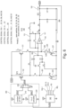
- FIG. 4 is an example diagram illustrating operation and switch settings of the reference voltage generator in a first mode (phase #1) according to embodiments herein.
- the switch controller 145 produces the control signal 105-1 and 105-1A to close switches S2, S3, S4, S6, and S8; the switch controller 145 produces the control signal 105-2 to open switches S1, S5, and S7.
- the source 295 represents an input offset voltage (Voff) of the amplifier 140.
- the switch control circuit 145 configures the amplifier 140 in a unity gain mode in which an output 141 of the amplifier 140 is coupled to an inverting input (-) of the amplifier 140.
- the switch control circuit 145 couples the first current driver 121 to the first component 221 via activation of switch S8.
- the first current driver 121 supplies (or drives) first current (such as I) through the switch S8 and the first component 221 (such as from respective emitter E to base B of a respective bipolar junction transistor) during the first mode to generate a first voltage Veb(I).
- Node 282 (connected to non-inverting input of amplifier 140) is set to voltage Veb(I) + Voffset.
- the second current driver 122 supplies (or drives) second current (such as NxI) through the switch S4 and the second component 222 (such as from respective emitter E to base B of a bipolar junction transistor) during the first mode to generate a second voltage Veb(NxI) that is inputted to the capacitor C3 through closed switch S6.
- second current such as NxI
- the switch S4 supplies (or drives) second current (such as NxI) through the switch S4 and the second component 222 (such as from respective emitter E to base B of a bipolar junction transistor) during the first mode to generate a second voltage Veb(NxI) that is inputted to the capacitor C3 through closed switch S6.
- the amplifier 140 when switch S3 is closed during phase #1, the amplifier 140 operates in a unity gain mode. Because the amplifier 140 operates in the unity gain (or buffer) mode, the inverting input (-) of the amplifier 140 is Veb(I) + Voffset.
- FIG. 5 is an example diagram illustrating connectivity of components in the reference voltage generator during the first mode (phase #1) according to embodiments herein.
- Capacitor C3 is coupled between the node 281 and the inverting input of the amplifier 140.
- Charge Q of a capacitor equals the voltage across the capacitor multiplied by the capacitance of the capacitor.
- phase #1 recall that the voltage at the inverting node of the amplifier 140 is Veb(I) + Voffset. Because the amplifier 140 operates in the unity gain mode, the inverting input of the amplifier 140 is Veb(I) + Voffset.
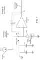
- FIG. 6 is an example diagram illustrating operation of the reference voltage generator in a second mode (phase #2) according to embodiments herein.
- the switch controller 145 In the second mode (phase #2), the switch controller 145 produces the control signals 105-1 and 105-1A to open switches S2, S3, S4, S6, and S8; the switch controller 145 produces the control signal 105-2 to close switches S1, S5, and S7.
- the switch control circuit 145 configures the amplifier 140 to operate in a gain mode in which the capacitor C1 is coupled in the feedback path 115 such as between the inverting input (-) of the amplifier 140 and the output 141 of the amplifier 140.
- the switch control circuit 145 is operable to couple the second current driver 122 to the first component 221 through switch S5.
- the first current driver 121 is deactivated and/or disconnected from the second semiconductor device 122 via opened switch S8.
- the second current driver 122 supplies the second current NxI through the first component 221 to generate a third voltage Veb(NI) at node 282 that is inputted to non-inverting input (+) of the amplifier 140.
- the capacitor C 1 is connected between the output 141 of the amplifier 140 and the inverting input (-) of the amplifier 140.
- FIG. 7 is an example diagram illustrating connectivity of components in the reference voltage generator during the second mode (phase #2) according to embodiments herein.
- charge Q of a capacitor equals the voltage across the capacitor multiplied by the capacitance of the capacitor.
- phase #2 the voltage at the non-inverting node of the amplifier 140 is Veb(NI) + Voffset. Because the amplifier 140 is balanced and is operating in the gain mode, the inverting input (-) or node 283 of the amplifier 140 is also Veb(NI) + Voffset.
- Qph2 Veb nI + Voff C 3 + Veb nI + Voff C 2 + Veb nI + Voff ⁇ Vo C 1
- Qph2 the total charge associated with capacitors C1, C2, and C3 in phase 2.
- Qph1 Qph2.
- the settings of the capacitors C1, C2, and C3 can be chosen to produce a voltage reference at a desired setpoint.
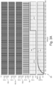
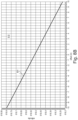
- FIG. 8A is an example diagram illustrating a theoretical magnitude of the generated reference voltage over a range of temperature according to embodiments herein.
- a magnitude of the reference voltage 150 is substantially constant over a range of temperature.
- the magnitude of the reference voltage is less than 1 VDC (Volts DC), although the magnitude of the reference voltage 150 can be any suitable value.
- the magnitude of the reference voltage 150 varies between 617 and 618.5 millivolts over a wide range of temperatures (such as -40 degrees Celsius and 125 degrees Celsius).
- FIG. 8B is an example diagram illustrating that a magnitude of the output voltage is substantially constant over different offset voltages according to embodiments herein.
- graph 810 and line 820 illustrates the change in magnitude of the output reference voltage 150 versus change in input offset voltage.
- the offset voltage is swept from -10mV to +10mV.
- the Voffset labelled 295 in FIG. 4 and the offset voltage of the operational amplifier in FIG. 2B are being swept simultaneously.
- the output reference voltage 150 (Vref) is seen to have an almost constant value of 0.618V. There is very slight deviation in Vref and illustrates that the auto zero method of offset (switching of capacitor C1) cancellation works correctly
- FIG. 8C illustrates the temperature behavior of the output voltage reference 150 set to the target voltage of 747mV at room temperature according to embodiments herein.
- C1 1pF
- C3 0.6pF
- the best suitable value for C2 was found to be 4.8pF.
- a circuit designer implementing the reference voltage generator 100 selects a suitable value of C2 to get a suitable temperature behavior of the output reference voltage. Note that the supply voltage for the circuit will have to be greater than 1.2VDC in this situation to accommodate generating the 1.2VDC reference voltage.
- FIG. 9 is a flowchart 900 illustrating an example method according to embodiments herein. Note that there will be some overlap with respect to concepts as discussed above.
- the switch controller 145 In processing operation 910, the switch controller 145 generates control signals 105 105-1A, etc., to control the switch network (such as switches S1, S2, etc.) of the reference voltage generator 100.
- the reference voltage generator 100 includes an amplifier 140 and a capacitor C1.
- the switch controller 145 In processing operation 920, during a first mode (such as phase #1) of controlling operation of the reference voltage generator 100, the switch controller 145: i) produces the control signals 105 to disconnect the capacitor C1 from the feedback path 115 of the amplifier 140, and ii) charges the capacitor C1.
- the switch controller 145 produces the control signals 105 to insert the capacitor C 1 into the feedback path of the amplifier 140 to produce the reference voltage 150.
Landscapes
- Engineering & Computer Science (AREA)
- Physics & Mathematics (AREA)
- Electromagnetism (AREA)
- General Physics & Mathematics (AREA)
- Radar, Positioning & Navigation (AREA)
- Automation & Control Theory (AREA)
- Power Engineering (AREA)
- Microelectronics & Electronic Packaging (AREA)
- Nonlinear Science (AREA)
- Amplifiers (AREA)
Claims (6)
- Générateur d'une tension de référence comprenant :un amplificateur (140) opérationnel ayant une sortie (141) sur laquelle une tension (Vref) de référence est générée ;un premier condensateur (C1) ayant une première borne connectée à une entrée inverseuse de l'amplificateur (140) opérationnel ;une unité (145) de commande d'interrupteur configurée pour commander la connectivité du premier condensateur (C1) dans un chemin (115) de réaction de l'amplificateur (140) opérationnel ;un premier dispositif (221) à semiconducteur monté entre un premier noeud (282) et un noeud de référence de terre, le premier noeud correspondant à une entrée non inverseuse de l'amplificateur (140) opérationnel ;un premier circuit (121) d'attaque de courant monté entre un premier noeud (Vdd) de tension d'entrée et le premier noeud (282) et configuré pour produire un premier courant (I) ;un deuxième condensateur (C3) ayant une première borne connectée à l'entrée inverseuse de l'amplificateur (140) opérationnel ;un troisième condensateur (C2) monté entre l'entrée inverseuse de l'amplificateur (140) opérationnel et le noeud de référence de terre ;un deuxième dispositif (222) à semiconducteur monté entre un deuxième noeud (281) et le noeud de référence de terre ;un deuxième circuit (122) d'attaque de courant monté entre le premier noeud (Vdd) de tension d'entrée et le deuxième noeud (281) et configuré pour produire un deuxième courant (N*I) égal à un multiple du premier courant (I) ;un premier interrupteur (S1) monté entre une deuxième borne du premier condensateur (C1) et la sortie (141) de l'amplificateur (140) opérationnel ;un deuxième interrupteur (S2) monté entre la deuxième borne du premier condensateur (C1) et le noeud de référence de terre ;un troisième interrupteur (S3) monté entre la sortie de l'amplificateur (140) opérationnel et son entrée inverseuse ;un quatrième interrupteur (S4) ayant une première borne connectée au deuxième circuit (122) d'attaque de courant et une deuxième borne connectée au deuxième noeud (281) ;un cinquième interrupteur (S5) monté entre le premier noeud (282) et la première borne du quatrième interrupteur ;un sixième interrupteur (S6) monté entre une deuxième borne du deuxième condensateur (C3) et le deuxième noeud (281) ;un septième interrupteur (S7) monté entre la deuxième borne du deuxième condensateur (C3) et la tension de référence de terre ;un huitième interrupteur (S8) monté entre le premier circuit (121) d'attaque de courant et le premier noeud (282),dans lequel l'unité (145) de commande d'interrupteur est configurée pour commuter entre :i) un premier mode, dans lequel, en fermant les deuxième, troisième, quatrième, sixième et huitième interrupteurs (S2, S3, S4, S6, S8) et en ouvrant les premier, cinquième et septième interrupteurs (S1, S5, S7), le premier condensateur (C1) est absent du chemin (115) de réaction de l'amplificateur (140) opérationnel et est chargé, et dans lequel l'amplificateur (140) opérationnel fonctionne dans un mode de gain unité, dans lequel une sortie (141) de l'amplificateur (140) opérationnel est reliée à une entrée inverseuse de l'amplificateur (140) opérationnel, etii) un deuxième mode, dans lequel, en fermant les premier, cinquième et septième interrupteurs (S1, S5, S7) et en ouvrant les deuxième, troisième, quatrième, sixième et huitième interrupteurs (S2, S3, S4, S6, S8), le premier condensateur (C1) chargé est inséré dans le chemin (115) de réaction de l'amplificateur (140) opérationnel et dans lequel l'amplificateur (140) opérationnel fonctionne dans un mode de gain, dans lequel le premier condensateur (C1) est monté entre l'entrée inverseuse de l'amplificateur (140) et la sortie (141) de l'amplificateur (140) opérationnel,dans lequel l'unité (145) de commande d'interrupteur est configurée en outre pour, pendant le premier mode, connecter le premier circuit (121) d'attaque de courant au premier dispositif (221) à semiconducteur, le premier circuit (121) d'attaque de courant fournissant le premier courant (I) dans le premier dispositif (221) à semiconducteur pendant le premier mode pour générer une première tension aux bornes du premier dispositif (221) à semiconducteur, la première tension étant entrée dans l'entrée non inverseuse de l'amplificateur (140) opérationnel,dans lequel l'unité (145) de commande d'interrupteur est configurée en outre pour, pendant le premier mode, connecter le deuxième circuit (122) d'attaque de courant au deuxième dispositif (222) à semiconducteur, le deuxième circuit (122) d'attaque de courant fournissant le deuxième courant (N* 1) dans le deuxième dispositif (222) à semiconducteur pendant le premier mode pour créer une deuxième tension aux bornes du deuxième dispositif (222) à semiconducteur, la deuxième tension étant entrée dans le deuxième condensateur (C3),dans lequel le deuxième condensateur (C3) est, pendant le premier mode, monté entre le deuxième dispositif (222) à semiconducteur et l'entrée inverseuse de l'amplificateur (140) opérationnel,dans lequel l'unité (145) de commande d'interrupteur est configurée en outre pour, pendant le deuxième mode, déconnecter la premier circuit (121) d'attaque de courant du premier dispositif (221) à semiconducteur et le deuxième circuit (122) d'attaque de courant du deuxième dispositif (222) à semiconducteur, etdans lequel le générateur d'une tension de référence comprend en outre :
un circuit (265) de polarisation configuré pour commuter chacun du premier circuit (121) d'attaque de courant et du deuxième circuit (122) d'attaque de courant entre attaquer sur la base d'un premier signal de polarisation et d'un deuxième signal de polarisation, le premier signal de polarisation étant un signal constant configuré pour initialiser un fonctionnement du générateur d'une tension de référence pour produire la tension de référence pour produire la tension de référence, le deuxième signal de polarisation étant généré par l'intermédiaire d'un convertisseur tension à courant sur la base de la tension (Vref) de référence. - Générateur d'une tension de référence suivant la revendication 1, dans lequel, pendant le deuxième mode, l'unité (145) de commande d'interrupteur est configurée pour relier le deuxième circuit (122) d'attaque de courant au premier dispositif (221) à semiconducteur, le deuxième circuit (122) d'attaque de courant fournissant du courant dans le premier dispositif (221) à semiconducteur dans le deuxième mode pour générer une deuxième tension entrée dans l'entrée non inverseuse de l'amplificateur (140) opérationnel.
- Générateur d'une tension de référence suivant la revendication 1, dans lequel un facteur de surface du premier dispositif (221) à semiconducteur est sensiblement égal à un facteur de surface du deuxième dispositif (222) à semiconducteur.
- Générateur d'une tension de référence suivant l'une quelconque des revendications 1 à 3,dans lequel une amplitude de la tension de référence est sensiblement constante sur une plage de température ; etdans lequel une amplitude de la tension de référence est plus petite que 1 V en courant continu.
- Générateur d'une tension de référence suivant la revendication 1, comprenant en outre
un troisième condensateur (C3) ; etdans lequel chacun du premier condensateur (C1), du deuxième condensateur (C2) et du troisième condensateur (C3) est relié à une entrée inverseuse de l'amplificateur (140) opérationnel ; etdans lequel le premier condensateur (C1) et le deuxième condensateur (C2) sont montés en parallèle pendant le premier mode ; etdans lequel le deuxième condensateur (C2) et le troisième condensateur (C3) sont montés en parallèle pendant le deuxième mode. - Procédé comprenant :générer des signaux de commande pour commander un générateur (100) d'une tension de référence,dans lequel le générateur (100) d'une tension de référence comprend :un amplificateur (140) opérationnel ayant une sortie (141) sur laquelle une tension (Vref) de référence est générée ;un premier condensateur (C1) ayant une première borne connectée à une entrée inverseuse de l'amplificateur (140) opérationnel ;un premier dispositif (221) à semiconducteur monté entre un premier noeud (282) et un noeud de référence de terre, le premier noeud correspondant à une entrée non inverseuse de l'amplificateur (140) opérationnel ;un premier circuit (121) d'attaque de courant monté entre un premier noeud (Vdd) de tension d'entrée et le premier noeud (282) et configuré pour produire un premier courant (I) ;un deuxième condensateur (C3) ayant une première borne connectée à l'entrée inverseuse de l'amplificateur (140) opérationnel ;un troisième condensateur (C2) monté entre l'entrée inverseuse de l'amplificateur (140) opérationnel et le noeud de référence de terre ;un deuxième dispositif (222) à semiconducteur monté entre un deuxième noeud (281) et le noeud de référence de terre ;un deuxième circuit (122) d'attaque de courant monté entre le premier noeud (Vdd) de tension d'entrée et le deuxième noeud (281) et configuré pour produire un deuxième courant (N*I) égal à un multiple du premier courant (I) ;un premier interrupteur (S1) monté entre une deuxième borne du premier condensateur (C1) et la sortie (141) de l'amplificateur (140) opérationnel ;un deuxième interrupteur (S2) monté entre la deuxième borne du premier condensateur (C1) et le noeud de référence de terre ;un troisième interrupteur (S3) monté entre la sortie de l'amplificateur (140) opérationnel et son entrée inverseuse ;un quatrième interrupteur (S4) ayant une première borne connectée au deuxième circuit (122) d'attaque de courant et une deuxième borne connectée au deuxième noeud (281) ;un cinquième interrupteur (S5) monté entre le premier noeud (282) et la première borne du quatrième interrupteur ;un sixième interrupteur (S6) monté entre une deuxième borne du deuxième condensateur (C3) et le deuxième noeud (281) ;un septième interrupteur (S7) monté entre la deuxième borne du deuxième condensateur (C3) et la tension de référence de terre ;un huitième interrupteur (S8) monté entre le premier circuit (121) d'attaque de courant et le premier noeud (282), etdans lequel les signaux de commande comprennent :i) pendant un premier mode de commande du générateur (100) d'une tension de référence, produire les signaux de commande pour déconnecter le premier condensateur (C1) d'un chemin (115) de réaction de l'amplificateur (140) opérationnel en fermant les deuxième, troisième, quatrième, sixième et huitième interrupteurs (S2, S3, S4, S6, S8) et en ouvrant les premier, cinquième et septième interrupteurs (S1, S5, S7), et charger le premier condensateur (C1), et pour faire fonctionner l'amplificateur (140) opérationnel dans un mode de gain unité, dans lequel une sortie (141) de l'amplificateur (140) opérationnel est reliée à une entrée inverseuse de l'amplificateur (140) opérationnel ; etii) pendant un deuxième mode de commande du générateur d'une tension de référence (100), produire les signaux de commande pour insérer le premier condensateur (C1) chargé dans le chemin (115) de réaction de l'amplificateur (140) opérationnel, en fermant les premier, cinquième et septième interrupteurs (S1, S5, S7) et en ouvrant les deuxième, troisième, quatrième, sixième et huitième interrupteurs (S2, S3, S4, S6, S8) pour produire une tension de référence, et pour faire fonctionner l'amplificateur (140) opérationnel dans un mode de gain, dans lequel le premier condensateur (C1) est monté entre l'entrée inverseuse de l'amplificateur (140) opérationnel et la sortie (141) de l'amplificateur (140) opérationnel,dans lequel générer les signaux de commande pendant le premier mode comprend en outre produire les signaux de commandepour relier le premier circuit (121) d'attaque de courant au premier dispositif (221) à semiconducteur, le premier circuit (121) d'attaque de courant fournissant le premier courant (I) dans le premier dispositif (221) à semiconducteur pendant le premier mode pour générer une première tension aux bornes du premier dispositif (221) à semiconducteur, la première tension étant entrée dans l'entrée non inverseuse de l'amplificateur (140) opérationnel, etpour relier le deuxième circuit (122) d'attaque de courant au deuxième dispositif (222) à semiconducteur, le deuxième circuit (122) d'attaque de courant fournissant le deuxième courant (N*I) dans le deuxième dispositif (222) à semiconducteur pendant le premier mode pour générer une deuxième tension aux bornes du deuxième dispositif (222) à semiconducteur, la deuxième tension étant entrée dans le deuxième condensateur (C3),dans lequel le deuxième condensateur (C3) est, pendant le premier mode, monté entre le deuxième dispositif (222) à semiconducteur et l'entrée inverseuse de l'amplificateur opérationnel,dans lequel générer les signaux de commande pendant le deuxième mode comprend en outre produire les signaux de commande pour déconnecter le premier circuit (121) d'attaque de courant du premier dispositif (221) à semiconducteur et le deuxième dispositif (122) d'attaque de courant du deuxième dispositif (222) à semiconducteur, etdans lequel le procédé comprend en outre :
commuter chacun du premier circuit (121) d'attaque de courant et du deuxième circuit (122) d'attaque de courant, entre attaquer sur la base d'un premier signal de polarisation et d'un deuxième signal de polarisation, le premier signal de polarisation étant un signal constant configuré pour initialiser un fonctionnement du générateur d'une tension de référence pour produire la tension de référence, le deuxième signal de polarisation étant généré par l'intermédiaire d'un convertisseur tension à courant sur la base de la tension (Vref) de référence.
Applications Claiming Priority (1)
| Application Number | Priority Date | Filing Date | Title |
|---|---|---|---|
| US16/238,776 US10852758B2 (en) | 2019-01-03 | 2019-01-03 | Reference voltage generator |
Publications (3)
| Publication Number | Publication Date |
|---|---|
| EP3677982A2 EP3677982A2 (fr) | 2020-07-08 |
| EP3677982A3 EP3677982A3 (fr) | 2020-10-21 |
| EP3677982B1 true EP3677982B1 (fr) | 2024-10-23 |
Family
ID=68944270
Family Applications (1)
| Application Number | Title | Priority Date | Filing Date |
|---|---|---|---|
| EP19217070.2A Active EP3677982B1 (fr) | 2019-01-03 | 2019-12-17 | Générateur de tension de référence |
Country Status (3)
| Country | Link |
|---|---|
| US (1) | US10852758B2 (fr) |
| EP (1) | EP3677982B1 (fr) |
| CN (1) | CN111399575B (fr) |
Families Citing this family (3)
| Publication number | Priority date | Publication date | Assignee | Title |
|---|---|---|---|---|
| US11205338B2 (en) * | 2019-12-19 | 2021-12-21 | Micron Technology, Inc. | Extracting the resistor-capacitor time constant of an electronic circuit line |
| US11392156B2 (en) * | 2019-12-24 | 2022-07-19 | Shenzhen GOODIX Technology Co., Ltd. | Voltage generator with multiple voltage vs. temperature slope domains |
| US11290674B1 (en) * | 2020-12-18 | 2022-03-29 | Omnivision Technologies, Inc. | Column amplifier capacitor switch circuit to adjust analog gain |
Family Cites Families (15)
| Publication number | Priority date | Publication date | Assignee | Title |
|---|---|---|---|---|
| US4375595A (en) | 1981-02-03 | 1983-03-01 | Motorola, Inc. | Switched capacitor temperature independent bandgap reference |
| US5059820A (en) * | 1990-09-19 | 1991-10-22 | Motorola, Inc. | Switched capacitor bandgap reference circuit having a time multiplexed bipolar transistor |
| IT1246598B (it) * | 1991-04-12 | 1994-11-24 | Sgs Thomson Microelectronics | Circuito di riferimento di tensione a band-gap campionato |
| AT403532B (de) | 1994-06-24 | 1998-03-25 | Semcotec Handel | Verfahren zur temperaturstabilisierung |
| US5982221A (en) | 1997-08-13 | 1999-11-09 | Analog Devices, Inc. | Switched current temperature sensor circuit with compounded ΔVBE |
| US5867012A (en) | 1997-08-14 | 1999-02-02 | Analog Devices, Inc. | Switching bandgap reference circuit with compounded ΔV.sub.βΕ |
| US6097239A (en) | 1999-02-10 | 2000-08-01 | Analog Devices, Inc. | Decoupled switched current temperature circuit with compounded ΔV be |
| US6819163B1 (en) | 2003-03-27 | 2004-11-16 | Ami Semiconductor, Inc. | Switched capacitor voltage reference circuits using transconductance circuit to generate reference voltage |
| US7112948B2 (en) * | 2004-01-30 | 2006-09-26 | Analog Devices, Inc. | Voltage source circuit with selectable temperature independent and temperature dependent voltage outputs |
| US7009373B1 (en) | 2004-04-13 | 2006-03-07 | Analog Devices, Inc. | Switched capacitor bandgap reference circuit |
| JP4681983B2 (ja) * | 2005-08-19 | 2011-05-11 | 富士通セミコンダクター株式会社 | バンドギャップ回路 |
| US8102205B2 (en) | 2009-08-04 | 2012-01-24 | Qualcomm, Incorporated | Amplifier module with multiple operating modes |
| US8461912B1 (en) * | 2011-12-20 | 2013-06-11 | Atmel Corporation | Switched-capacitor, curvature-compensated bandgap voltage reference |
| US9013231B1 (en) * | 2013-12-06 | 2015-04-21 | Atmel Corporation | Voltage reference with low sensitivity to package shift |
| US10054968B2 (en) | 2016-09-15 | 2018-08-21 | Xilinx, Inc. | Area-efficient high-accuracy bandgap voltage reference circuit |
-
2019
- 2019-01-03 US US16/238,776 patent/US10852758B2/en active Active
- 2019-12-17 EP EP19217070.2A patent/EP3677982B1/fr active Active
-
2020
- 2020-01-03 CN CN202010004587.9A patent/CN111399575B/zh active Active
Also Published As
| Publication number | Publication date |
|---|---|
| US10852758B2 (en) | 2020-12-01 |
| US20200218299A1 (en) | 2020-07-09 |
| CN111399575B (zh) | 2023-02-24 |
| EP3677982A3 (fr) | 2020-10-21 |
| CN111399575A (zh) | 2020-07-10 |
| EP3677982A2 (fr) | 2020-07-08 |
Similar Documents
| Publication | Publication Date | Title |
|---|---|---|
| US9991782B2 (en) | Control of conversion ratios of a power source block and bidirectional active filter | |
| US8154268B2 (en) | Switching regulator with balanced control configuration with filtering and referencing to eliminate compensation | |
| US10193449B2 (en) | Buck voltage converter | |
| EP3677982B1 (fr) | Générateur de tension de référence | |
| US9484809B2 (en) | Apparatus and methods for low voltage high PSRR systems | |
| US8970270B2 (en) | Duty cycle adjusting circuit and adjusting method | |
| EP2320296A1 (fr) | Circuit permettant de générer une tension de référence avec une compensation de la tension de suppression | |
| CN114094999B (zh) | 转换器电路、对应设备以及方法 | |
| US9444468B2 (en) | Oscillator devices and methods | |
| JP7058326B2 (ja) | スイッチング電源、半導体集積回路装置、差動入力回路 | |
| KR100651150B1 (ko) | 중간 또는 고주파수용 지연 클록 펄스폭 조정회로 | |
| US20190207573A1 (en) | Chopper-stabilized amplifier with analog-driven level shifter | |
| KR100750650B1 (ko) | 튜닝 회로. | |
| CN107342685B (zh) | Dcdc转换器 | |
| US11984849B2 (en) | Switchover schemes for transition of oscillator from internal-resistor to external-resistor mode | |
| US6111440A (en) | Circuit for generating interleaved ramped voltage signals having uniform, controlled maximum amplitude | |
| US7274182B2 (en) | Spring modulation with fast load-transient response for a voltage regulator | |
| US9705485B1 (en) | High-resolution current and method for generating a current | |
| IT202100017048A1 (it) | Circuiti e procedimenti di convertitore elettronico | |
| JP4504930B2 (ja) | チャージポンプ回路 | |
| CN116915030A (zh) | 用于谐振开关电容转换器的控制模块和对应的控制方法 | |
| CN113394968A (zh) | 电荷泵电路 | |
| EP2065780A1 (fr) | Ensemble de pompe à charge contrôlée et procédé pour le contrôle d'une pompe à charge synchronisée | |
| CN110661416A (zh) | 调节的高电压参考 | |
| US7498874B1 (en) | Glitch-free start-up with a tracking pin |
Legal Events
| Date | Code | Title | Description |
|---|---|---|---|
| PUAI | Public reference made under article 153(3) epc to a published international application that has entered the european phase |
Free format text: ORIGINAL CODE: 0009012 |
|
| STAA | Information on the status of an ep patent application or granted ep patent |
Free format text: STATUS: THE APPLICATION HAS BEEN PUBLISHED |
|
| AK | Designated contracting states |
Kind code of ref document: A2 Designated state(s): AL AT BE BG CH CY CZ DE DK EE ES FI FR GB GR HR HU IE IS IT LI LT LU LV MC MK MT NL NO PL PT RO RS SE SI SK SM TR |
|
| AX | Request for extension of the european patent |
Extension state: BA ME |
|
| PUAL | Search report despatched |
Free format text: ORIGINAL CODE: 0009013 |
|
| AK | Designated contracting states |
Kind code of ref document: A3 Designated state(s): AL AT BE BG CH CY CZ DE DK EE ES FI FR GB GR HR HU IE IS IT LI LT LU LV MC MK MT NL NO PL PT RO RS SE SI SK SM TR |
|
| AX | Request for extension of the european patent |
Extension state: BA ME |
|
| RIC1 | Information provided on ipc code assigned before grant |
Ipc: G05F 3/30 20060101AFI20200915BHEP |
|
| STAA | Information on the status of an ep patent application or granted ep patent |
Free format text: STATUS: REQUEST FOR EXAMINATION WAS MADE |
|
| 17P | Request for examination filed |
Effective date: 20210421 |
|
| RBV | Designated contracting states (corrected) |
Designated state(s): AL AT BE BG CH CY CZ DE DK EE ES FI FR GB GR HR HU IE IS IT LI LT LU LV MC MK MT NL NO PL PT RO RS SE SI SK SM TR |
|
| STAA | Information on the status of an ep patent application or granted ep patent |
Free format text: STATUS: EXAMINATION IS IN PROGRESS |
|
| 17Q | First examination report despatched |
Effective date: 20220601 |
|
| GRAP | Despatch of communication of intention to grant a patent |
Free format text: ORIGINAL CODE: EPIDOSNIGR1 |
|
| STAA | Information on the status of an ep patent application or granted ep patent |
Free format text: STATUS: GRANT OF PATENT IS INTENDED |
|
| INTG | Intention to grant announced |
Effective date: 20231215 |
|
| GRAJ | Information related to disapproval of communication of intention to grant by the applicant or resumption of examination proceedings by the epo deleted |
Free format text: ORIGINAL CODE: EPIDOSDIGR1 |
|
| STAA | Information on the status of an ep patent application or granted ep patent |
Free format text: STATUS: EXAMINATION IS IN PROGRESS |
|
| INTC | Intention to grant announced (deleted) | ||
| GRAJ | Information related to disapproval of communication of intention to grant by the applicant or resumption of examination proceedings by the epo deleted |
Free format text: ORIGINAL CODE: EPIDOSDIGR1 |
|
| GRAP | Despatch of communication of intention to grant a patent |
Free format text: ORIGINAL CODE: EPIDOSNIGR1 |
|
| GRAS | Grant fee paid |
Free format text: ORIGINAL CODE: EPIDOSNIGR3 |
|
| GRAS | Grant fee paid |
Free format text: ORIGINAL CODE: EPIDOSNIGR3 |
|
| STAA | Information on the status of an ep patent application or granted ep patent |
Free format text: STATUS: GRANT OF PATENT IS INTENDED |
|
| GRAP | Despatch of communication of intention to grant a patent |
Free format text: ORIGINAL CODE: EPIDOSNIGR1 |
|
| INTG | Intention to grant announced |
Effective date: 20240607 |
|
| P01 | Opt-out of the competence of the unified patent court (upc) registered |
Free format text: CASE NUMBER: APP_43361/2024 Effective date: 20240724 |
|
| GRAA | (expected) grant |
Free format text: ORIGINAL CODE: 0009210 |
|
| STAA | Information on the status of an ep patent application or granted ep patent |
Free format text: STATUS: THE PATENT HAS BEEN GRANTED |
|
| AK | Designated contracting states |
Kind code of ref document: B1 Designated state(s): AL AT BE BG CH CY CZ DE DK EE ES FI FR GB GR HR HU IE IS IT LI LT LU LV MC MK MT NL NO PL PT RO RS SE SI SK SM TR |
|
| REG | Reference to a national code |
Ref country code: GB Ref legal event code: FG4D |
|
| REG | Reference to a national code |
Ref country code: CH Ref legal event code: EP |
|
| REG | Reference to a national code |
Ref country code: DE Ref legal event code: R096 Ref document number: 602019060738 Country of ref document: DE |
|
| REG | Reference to a national code |
Ref country code: IE Ref legal event code: FG4D |
|
| REG | Reference to a national code |
Ref country code: LT Ref legal event code: MG9D |
|
| REG | Reference to a national code |
Ref country code: NL Ref legal event code: MP Effective date: 20241023 |
|
| REG | Reference to a national code |
Ref country code: AT Ref legal event code: MK05 Ref document number: 1735354 Country of ref document: AT Kind code of ref document: T Effective date: 20241023 |
|
| PG25 | Lapsed in a contracting state [announced via postgrant information from national office to epo] |
Ref country code: NL Free format text: LAPSE BECAUSE OF FAILURE TO SUBMIT A TRANSLATION OF THE DESCRIPTION OR TO PAY THE FEE WITHIN THE PRESCRIBED TIME-LIMIT Effective date: 20241023 |
|
| REG | Reference to a national code |
Ref country code: DE Ref legal event code: R081 Ref document number: 602019060738 Country of ref document: DE Owner name: CIRRUS LOGIC INTERNATIONAL SEMICONDUCTOR LTD., GB Free format text: FORMER OWNER: INFINEON TECHNOLOGIES AUSTRIA AG, VILLACH, AT |
|
| PG25 | Lapsed in a contracting state [announced via postgrant information from national office to epo] |
Ref country code: NL Free format text: LAPSE BECAUSE OF FAILURE TO SUBMIT A TRANSLATION OF THE DESCRIPTION OR TO PAY THE FEE WITHIN THE PRESCRIBED TIME-LIMIT Effective date: 20241023 |
|
| PG25 | Lapsed in a contracting state [announced via postgrant information from national office to epo] |
Ref country code: IS Free format text: LAPSE BECAUSE OF FAILURE TO SUBMIT A TRANSLATION OF THE DESCRIPTION OR TO PAY THE FEE WITHIN THE PRESCRIBED TIME-LIMIT Effective date: 20250223 Ref country code: HR Free format text: LAPSE BECAUSE OF FAILURE TO SUBMIT A TRANSLATION OF THE DESCRIPTION OR TO PAY THE FEE WITHIN THE PRESCRIBED TIME-LIMIT Effective date: 20241023 Ref country code: PT Free format text: LAPSE BECAUSE OF FAILURE TO SUBMIT A TRANSLATION OF THE DESCRIPTION OR TO PAY THE FEE WITHIN THE PRESCRIBED TIME-LIMIT Effective date: 20250224 |
|
| PG25 | Lapsed in a contracting state [announced via postgrant information from national office to epo] |
Ref country code: FI Free format text: LAPSE BECAUSE OF FAILURE TO SUBMIT A TRANSLATION OF THE DESCRIPTION OR TO PAY THE FEE WITHIN THE PRESCRIBED TIME-LIMIT Effective date: 20241023 |
|
| PG25 | Lapsed in a contracting state [announced via postgrant information from national office to epo] |
Ref country code: BG Free format text: LAPSE BECAUSE OF FAILURE TO SUBMIT A TRANSLATION OF THE DESCRIPTION OR TO PAY THE FEE WITHIN THE PRESCRIBED TIME-LIMIT Effective date: 20241023 |
|
| PG25 | Lapsed in a contracting state [announced via postgrant information from national office to epo] |
Ref country code: ES Free format text: LAPSE BECAUSE OF FAILURE TO SUBMIT A TRANSLATION OF THE DESCRIPTION OR TO PAY THE FEE WITHIN THE PRESCRIBED TIME-LIMIT Effective date: 20241023 |
|
| PG25 | Lapsed in a contracting state [announced via postgrant information from national office to epo] |
Ref country code: NO Free format text: LAPSE BECAUSE OF FAILURE TO SUBMIT A TRANSLATION OF THE DESCRIPTION OR TO PAY THE FEE WITHIN THE PRESCRIBED TIME-LIMIT Effective date: 20250123 |
|
| PG25 | Lapsed in a contracting state [announced via postgrant information from national office to epo] |
Ref country code: LV Free format text: LAPSE BECAUSE OF FAILURE TO SUBMIT A TRANSLATION OF THE DESCRIPTION OR TO PAY THE FEE WITHIN THE PRESCRIBED TIME-LIMIT Effective date: 20241023 Ref country code: GR Free format text: LAPSE BECAUSE OF FAILURE TO SUBMIT A TRANSLATION OF THE DESCRIPTION OR TO PAY THE FEE WITHIN THE PRESCRIBED TIME-LIMIT Effective date: 20250124 Ref country code: AT Free format text: LAPSE BECAUSE OF FAILURE TO SUBMIT A TRANSLATION OF THE DESCRIPTION OR TO PAY THE FEE WITHIN THE PRESCRIBED TIME-LIMIT Effective date: 20241023 |
|
| PG25 | Lapsed in a contracting state [announced via postgrant information from national office to epo] |
Ref country code: PL Free format text: LAPSE BECAUSE OF FAILURE TO SUBMIT A TRANSLATION OF THE DESCRIPTION OR TO PAY THE FEE WITHIN THE PRESCRIBED TIME-LIMIT Effective date: 20241023 |
|
| PG25 | Lapsed in a contracting state [announced via postgrant information from national office to epo] |
Ref country code: RS Free format text: LAPSE BECAUSE OF FAILURE TO SUBMIT A TRANSLATION OF THE DESCRIPTION OR TO PAY THE FEE WITHIN THE PRESCRIBED TIME-LIMIT Effective date: 20250123 |
|
| REG | Reference to a national code |
Ref country code: GB Ref legal event code: 732E Free format text: REGISTERED BETWEEN 20250403 AND 20250409 |
|
| PG25 | Lapsed in a contracting state [announced via postgrant information from national office to epo] |
Ref country code: SM Free format text: LAPSE BECAUSE OF FAILURE TO SUBMIT A TRANSLATION OF THE DESCRIPTION OR TO PAY THE FEE WITHIN THE PRESCRIBED TIME-LIMIT Effective date: 20241023 |
|
| PG25 | Lapsed in a contracting state [announced via postgrant information from national office to epo] |
Ref country code: MC Free format text: LAPSE BECAUSE OF FAILURE TO SUBMIT A TRANSLATION OF THE DESCRIPTION OR TO PAY THE FEE WITHIN THE PRESCRIBED TIME-LIMIT Effective date: 20241023 |
|
| PG25 | Lapsed in a contracting state [announced via postgrant information from national office to epo] |
Ref country code: DK Free format text: LAPSE BECAUSE OF FAILURE TO SUBMIT A TRANSLATION OF THE DESCRIPTION OR TO PAY THE FEE WITHIN THE PRESCRIBED TIME-LIMIT Effective date: 20241023 |
|
| PG25 | Lapsed in a contracting state [announced via postgrant information from national office to epo] |
Ref country code: EE Free format text: LAPSE BECAUSE OF FAILURE TO SUBMIT A TRANSLATION OF THE DESCRIPTION OR TO PAY THE FEE WITHIN THE PRESCRIBED TIME-LIMIT Effective date: 20241023 |
|
| PG25 | Lapsed in a contracting state [announced via postgrant information from national office to epo] |
Ref country code: RO Free format text: LAPSE BECAUSE OF FAILURE TO SUBMIT A TRANSLATION OF THE DESCRIPTION OR TO PAY THE FEE WITHIN THE PRESCRIBED TIME-LIMIT Effective date: 20241023 |
|
| REG | Reference to a national code |
Ref country code: DE Ref legal event code: R097 Ref document number: 602019060738 Country of ref document: DE |
|
| PG25 | Lapsed in a contracting state [announced via postgrant information from national office to epo] |
Ref country code: SK Free format text: LAPSE BECAUSE OF FAILURE TO SUBMIT A TRANSLATION OF THE DESCRIPTION OR TO PAY THE FEE WITHIN THE PRESCRIBED TIME-LIMIT Effective date: 20241023 |
|
| PG25 | Lapsed in a contracting state [announced via postgrant information from national office to epo] |
Ref country code: CZ Free format text: LAPSE BECAUSE OF FAILURE TO SUBMIT A TRANSLATION OF THE DESCRIPTION OR TO PAY THE FEE WITHIN THE PRESCRIBED TIME-LIMIT Effective date: 20241023 |
|
| PG25 | Lapsed in a contracting state [announced via postgrant information from national office to epo] |
Ref country code: IT Free format text: LAPSE BECAUSE OF FAILURE TO SUBMIT A TRANSLATION OF THE DESCRIPTION OR TO PAY THE FEE WITHIN THE PRESCRIBED TIME-LIMIT Effective date: 20241023 |
|
| REG | Reference to a national code |
Ref country code: CH Ref legal event code: PL |
|
| PG25 | Lapsed in a contracting state [announced via postgrant information from national office to epo] |
Ref country code: LU Free format text: LAPSE BECAUSE OF NON-PAYMENT OF DUE FEES Effective date: 20241217 |
|
| PLBE | No opposition filed within time limit |
Free format text: ORIGINAL CODE: 0009261 |
|
| STAA | Information on the status of an ep patent application or granted ep patent |
Free format text: STATUS: NO OPPOSITION FILED WITHIN TIME LIMIT |
|
| PG25 | Lapsed in a contracting state [announced via postgrant information from national office to epo] |
Ref country code: SE Free format text: LAPSE BECAUSE OF FAILURE TO SUBMIT A TRANSLATION OF THE DESCRIPTION OR TO PAY THE FEE WITHIN THE PRESCRIBED TIME-LIMIT Effective date: 20241023 |
|
| 26N | No opposition filed |
Effective date: 20250724 |
|
| REG | Reference to a national code |
Ref country code: BE Ref legal event code: MM Effective date: 20241231 |
|
| PG25 | Lapsed in a contracting state [announced via postgrant information from national office to epo] |
Ref country code: BE Free format text: LAPSE BECAUSE OF NON-PAYMENT OF DUE FEES Effective date: 20241231 |
|
| PG25 | Lapsed in a contracting state [announced via postgrant information from national office to epo] |
Ref country code: FR Free format text: LAPSE BECAUSE OF NON-PAYMENT OF DUE FEES Effective date: 20241223 |
|
| PG25 | Lapsed in a contracting state [announced via postgrant information from national office to epo] |
Ref country code: CH Free format text: LAPSE BECAUSE OF NON-PAYMENT OF DUE FEES Effective date: 20241231 |
|
| PG25 | Lapsed in a contracting state [announced via postgrant information from national office to epo] |
Ref country code: IE Free format text: LAPSE BECAUSE OF NON-PAYMENT OF DUE FEES Effective date: 20241217 |
|
| PGFP | Annual fee paid to national office [announced via postgrant information from national office to epo] |
Ref country code: GB Payment date: 20251229 Year of fee payment: 7 |
|
| PGFP | Annual fee paid to national office [announced via postgrant information from national office to epo] |
Ref country code: DE Payment date: 20251229 Year of fee payment: 7 |