EP3679385B1 - Résonateurs à intervalle de boucle de spectroscopie par résonance de spin - Google Patents
Résonateurs à intervalle de boucle de spectroscopie par résonance de spin Download PDFInfo
- Publication number
- EP3679385B1 EP3679385B1 EP18853629.6A EP18853629A EP3679385B1 EP 3679385 B1 EP3679385 B1 EP 3679385B1 EP 18853629 A EP18853629 A EP 18853629A EP 3679385 B1 EP3679385 B1 EP 3679385B1
- Authority
- EP
- European Patent Office
- Prior art keywords
- resonator
- gap
- opening
- sample
- loop
- Prior art date
- Legal status (The legal status is an assumption and is not a legal conclusion. Google has not performed a legal analysis and makes no representation as to the accuracy of the status listed.)
- Active
Links
Images


Classifications
-
- G—PHYSICS
- G01—MEASURING; TESTING
- G01R—MEASURING ELECTRIC VARIABLES; MEASURING MAGNETIC VARIABLES
- G01R33/00—Arrangements or instruments for measuring magnetic variables
- G01R33/20—Arrangements or instruments for measuring magnetic variables involving magnetic resonance
- G01R33/28—Details of apparatus provided for in groups G01R33/44 - G01R33/64
- G01R33/32—Excitation or detection systems, e.g. using radio frequency signals
- G01R33/34—Constructional details, e.g. resonators, specially adapted to MR
- G01R33/343—Constructional details, e.g. resonators, specially adapted to MR of slotted-tube or loop-gap type
-
- G—PHYSICS
- G01—MEASURING; TESTING
- G01R—MEASURING ELECTRIC VARIABLES; MEASURING MAGNETIC VARIABLES
- G01R33/00—Arrangements or instruments for measuring magnetic variables
- G01R33/20—Arrangements or instruments for measuring magnetic variables involving magnetic resonance
- G01R33/60—Arrangements or instruments for measuring magnetic variables involving magnetic resonance using electron paramagnetic resonance
-
- H—ELECTRICITY
- H01—ELECTRIC ELEMENTS
- H01P—WAVEGUIDES; RESONATORS, LINES, OR OTHER DEVICES OF THE WAVEGUIDE TYPE
- H01P7/00—Resonators of the waveguide type
- H01P7/08—Strip line resonators
-
- G—PHYSICS
- G01—MEASURING; TESTING
- G01N—INVESTIGATING OR ANALYSING MATERIALS BY DETERMINING THEIR CHEMICAL OR PHYSICAL PROPERTIES
- G01N24/00—Investigating or analyzing materials by the use of nuclear magnetic resonance, electron paramagnetic resonance or other spin effects
- G01N24/10—Investigating or analyzing materials by the use of nuclear magnetic resonance, electron paramagnetic resonance or other spin effects by using electron paramagnetic resonance
Definitions
- Electron-Spin Resonance Spectroscopy also called Electron Paramagnetic Resonance Spectroscopy (EPR) is an analytical method that can be used to study the local atomic and molecular environment around unpaired electrons present in chemical species including organic and biomolecules containing metal atoms, as well as in any chemical species where radicals or unpaired electrons may be present, even transiently during a chemical reaction or other dynamic process.
- ESR Electron-Spin Resonance Spectroscopy
- EPR Electron Paramagnetic Resonance Spectroscopy
- a large magnetic field is applied to a sample of material to be analyzed, thereby inducing a spectral separation (splitting) of electron-spin states that otherwise may have the same energy as one another (degenerate states).
- Electromagnetic radiation generally in but not limited to the microwave spectral region is applied to the sample in the magnetic field, typically in combination with modulating the magnetic field, to make spectroscopic measurements of the sample, that is, to read a quantum state of the sample.
- Some ESR measurements can also be performed without the presence of an externally applied magnetic field, for example if the splitting between levels is induced by other effects, such as spin-orbit coupling.
- ESR is a sensitive spectroscopic technique that can be used to study very small quantities of matter.
- Loop-gap resonators are components used in Electron-Spin Resonance spectrometers to concentrate the oscillating magnetic field from the applied electromagnetic radiation on the sample being studied, thereby enhancing the sensitivity of the ESR measurements.
- Loop-gap resonators which are in a class of devices called "lumped-element" resonators, include both electrical inductance and capacitance in a single integrated structure that is generally constructed as a ring-shaped conductor having an interruption along its circumference.
- the loop which generally encircles the sample to be analyzed, provides electrical inductance, and the gap formed by the interruption in the loop contributes electrical capacitance, which together determine the resonant frequency of the resonator.
- the loop about the sample can be fabricated as an elongated cylinder having a gap in a wall of the cylinder along its axial length, or can be made as a substantially planar loop having an interruption of the loop in the plane.
- Such relatively planar loops can be fabricated using any additive or subtractive fabrication method such as photolithography, etching, machining, or photodeposition, and on any size scale accessible to the selected fabrication technology.
- quantum computing One field in which very small samples are studied is quantum computing, where advantage is taken of quantum properties such as superposition of states and quantum entanglement to dramatically enhance the ability to address certain classes of computational problems.
- Quantum computing is currently a very active area of technology development and defines a great need for new devices that can work with molecular-scale samples.
- loop-gap resonators are currently used in some ESR spectrometers for studying sample volumes on a microliter scale, continuing advancements in fields including biochemistry, nanotechnology and quantum computing have generated a need for the development of loop-gap resonators capable of supporting the ESR analysis of ever smaller samples.
- Prior art document US 2013/093424 A1 discloses a resonator system for electron spin resonance (ESR).
- the resonator system comprises: a generally planar resonator layer defining an open-loop gapped by a non-conductive gap in the layer, and a microwave feed, positioned configured for transmitting microwave to the resonator layer such as to concentrate, with a quality factor of at least 100, a magnetic field within an effective volume of less than 1 nL above the layer.
- One aspect of the present invention is a resonator for coupling electromagnetic radiation to a sample on the scale of a quantum object embodying a qubit.
- the resonator includes an electrically conductive member.
- An opening through the electrically conductive member defines an inductive loop of the resonator, and at least a portion of the sample can be positioned within the opening.
- An elongated, continuous gap following a convoluted path through the electrically conductive member extends between the opening and an outer boundary of the conductive member.
- the elongated gap contributes electrical capacitance to the resonator, wherein the convoluted path comprises a plurality of path segments and changes of direction therebetween, and wherein one or more of the changes of direction comprises a reversal of direction.
- the capacitance can be proportional to the length of the convoluted path, and inversely proportional to a width of the gap.
- the capacitance and inductance of the resonator together define a resonant frequency of the resonator.
- the resonator can be fabricated by various techniques.
- the conductive member can be a metallic or other conductive layer overlying a non-conductive or dielectric substrate.
- a dielectric material can overlie or coat a portion or all of the electrically conductive member, and can be fabricated to fill in all or part of the gap along the convoluted path. This overlying dielectric layer can be applied to modify (increase) the capacitance of the resonator.
- the resonator can be substantially planar, for example, as manufactured using microelectronic or thin-film fabrication techniques. Alternatively, the surface of the resonator can be non-planar or the resonator can be physically flexible.
- the resonator can also be fabricated from bulk materials, for example, as manufactured using mechanical, chemical, electrical or optical machining techniques.
- the continuous convoluted path can have any of several forms.
- the convoluted path can include any number of straight or curved length segments with changes of direction between them.
- the changes of direction can be reversals of direction between length segments, forming a zig-zag path where the conductive material on opposite sides of the gap can be described as interdigitated, that is, resembling the appearance of interlaced fingers of human hands.
- the capacitor is three dimensional, comprising two or more layers of conductive material defining a convoluted path and separated by dielectric layers, thereby facilitating the construction of resonators having even greater capacitance than is achievable with a single-layer conductor.
- the capacitance of a resonator of the present invention having a second conductive layer overlying and insulated from a first conductive layer can be designed to have more than twice the capacitance of a similarly-sized resonator having only a single conductive layer.
- the changes of direction between legs are illustrated in FIG. 2 as being abrupt, these transitions can also be smooth or curved within the scope of the present invention.
- the number of changes or reversals of direction can be up to 8, up to 38, or can be any number meeting engineering and resonator performance requirements for a particular application.
- the inventive resonators can have physically small dimensions, for example including gap widths smaller than 10 nanometers.
- a sample for use with the resonator can be as small as a single magnetic molecule.
- a system of the present invention is applicable to one or both of measuring and changing the quantum state of a qubit, such as can be used in a quantum computer.
- the system includes a resonator of the present invention, a sample positioned at least partially within the opening of the resonator, and external means for simultaneously applying a magnetic field and electromagnetic radiation at a resonant frequency of the resonator, for inducing a resonance in the sample.
- Another aspect of the present invention is a method for measuring and changing a quantum state of a sample on the scale of a quantum object embodying a qubit.
- the method includes positioning at least a portion of the sample within an opening of a loop-gap resonator having a capacitance defined by a convoluted gap, defining a convoluted path, extending between the opening and an outer edge of the resonator, simultaneously exposing the sample to a magnetic field and electromagnetic radiation and detecting a resonance signal from the sample, wherein the elongated gap contributes electrical capacitance to the resonator, wherein the convoluted path comprises a plurality of path segments and changes of direction therebetween, and wherein one or more of the changes of direction comprises a reversal of direction.
- the opening and the portion of the sample positioned in the opening can have physical dimensions as small as 10 nanometers or smaller.
- a loop-gap resonator advantageously enhances sensitivity of the measurement or reading of a quantum state and provides a large, fairly uniform, oscillating magnetic field at the location where the sample is positioned for analysis.
- FIG. 1 schematically illustrates a prior art loop-gap resonator 100 as could be used in an ESR spectrometer.
- the resonator 100 is seen to comprise an approximately circular conductive disc 102 having an outer substantially circumferential boundary 104 and an opening 106 through the disc 102, the opening 106 being located entirely within the boundary 104 and having an area suitable for receiving a sample therein.
- the resonator 100 is illustrated as substantially planar and viewed from above the plane, but can in principle have any thickness along an axis perpendicular to the plane.
- the sample being studied is positioned substantially within the opening 106.
- the conductive path about the opening 106 comprises the loop of the loop-gap resonator 100 and contributes inductance thereto.
- the resonator 100 is also seen to include a physical gap 108 that interrupts the loop about the opening 106 and extending from the opening 106 to the boundary 104, the gap 108 comprising capacitance.
- the loop-gap resonator 100 is thus substantially an LC resonator having a resonant frequency proportional to 1/sqrt(LC), where L represents inductance and C represents capacitance.
- the energies that correspond with a detectable splitting of the electronic spin states for ESR are broadly in the microwave radiation region of the electromagnetic spectrum, and are dependent on the strength of the applied magnetic field.
- the majority of commercial ESR spectrometers operate in what is generally called the X-band, in the frequency range of approximately 8 to 12 GHz (GigaHertz), but this is by no means limiting, and ESR measurements can in principle be made in any portion of the microwave and adjacent spectral regions, for example, extending to the radiofrequency (RF), millimeter-wave, Terahertz or optical frequency ranges.
- RF radiofrequency
- Microwave radiation is typically channeled to the resonator by waveguides or coaxial cables for making ESR measurements.
- the dimensions of the waveguides and the resonator are specific to the electromagnetic radiation frequency at which measurements are being made.
- Operating parameters of ESR measurement apparatus may include microwave power (amplitude), magnetic field strength and direction, sample orientation (in the case of crystalline samples), and the design of the resonator.
- the physical dimensions of a resonator in which a sample is positioned are preferably well matched to those of the sample.
- An aspect of the present invention is provision of a loop-gap resonator for studying very small samples, such as samples of rare or difficult-to-synthesize biochemical species, and nanoscale devices such as those used in the development of quantum information technology, where an objective is to make ESR measurements of quantum states of only a few or even a single atomic or molecular scale specie or one or more nanometer-scale artificially fabricated device, such as a quantum dot or a chemically synthesized magnetic molecule.
- Providing an extremely small cross-section loop in a loop-gap resonator is desirable for studying such samples. At any selected microwave frequency, reducing the dimensions of the loop reduces its inductance, and a correspondingly greater capacitance is required to maintain a target resonant frequency of the resonator.
- a loop-gap resonator 200 according to the present invention is illustrated schematically in FIG. 2 .
- the resonator 200 is seen to comprise a conductive disc 202 having an outer boundary 204 and a through opening 206, similar to the corresponding elements 102, 104 and 106 illustrated in FIG. 1 .
- loop-gap resonators according to the present invention can have any cross-sectional shape that meets engineering needs for a particular design of a loop-gap resonator.
- the opening 206 comprises the loop of the loop-gap resonator 200.
- inventive resonator 200 and other resonators disclosed herein, are for illustrative purposes shown in the Figures as substantially planar (for example, thin-film devices fabricated on a planar substrate) and viewed from above the plane, but the inventive resonators can in principle have any thickness perpendicular to the illustrated surface.
- resonators according to the present invention can have a curved surface, for example by being fabricated on a curved substrate surface, or can be fabricated from flexible materials so that the product device can be flexed or bent while maintaining functionality as a resonator. It is to be understood that all embodiments of resonators disclosed herein are intended to include curved as well as planar surfaces.
- the loop-gap resonator 200 of FIG. 2 includes a gap 208 comprising a convoluted path between the opening 206 and the boundary 204.
- the convoluted path is seen to comprise a plurality of legs 210 alternately extending in opposite directions, thus deviating from an imaginary straight path between the opening 206 and the boundary 204.
- the legs 210 are seen to be interconnected by turns 212 at their respective ends, illustrated in the Figure as reversing the direction of the continuous path.
- the interdigitated structure illustrated in FIG. 2 increases the capacitance approximately proportionally to the increase in the length of the path relative to that of the resonator illustrated in FIG. 1 , and allows the opening 206 to be correspondingly smaller for a given resonant frequency.
- a smaller opening (loop) provides an enhancement of the radiation magnetic field therein, where the sample is located. This design promises greater sensitivity and a corresponding ability to study smaller samples.
- a further feature of the interdigitated capacitor structure is that electrical current flows in opposite directions along alternate legs of the path, causing the corresponding magnetic fields to cancel out to first order. This results in a very low inductance of the capacitor.
- the inventive design enables the capacitance of the loop-gap resonator 200 to be dramatically increased without introducing significant parasitic inductance.
- the capacitance of a loop-gap resonator of the present invention can be tuned to a desired value by controlled placement or deposition of a dielectric material over or within the gap.
- a dielectric material that could be used in this manner is sapphire (alumina).
- the resonant frequency is lowered by addition of the overlying dielectric material.
- the number of turns 212 in direction along the path of the gap 208 is an even number. In a further embodiment, an even number of reversals in direction supports cancellation of magnetic fields along adjacent legs 210.
- the convoluted path can include any number of legs and any number of changes in direction therebetween that facilitate increasing the effective length of the path between an opening and a boundary of a loop-gap resonator according to the present invention.
- consecutive legs 210 are illustrated as being oriented approximately parallel to one another in FIG. 2
- consecutive legs can be oriented at non-zero angles to one another.
- the legs are themselves curved.
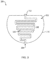
- FIG. 3 schematically illustrates another embodiment of a loop-gap resonator 300 according to the present invention, wherein an interdigitated capacitor structure 302 defines a convoluted path, illustrated as a zig-zag path, along a gap 304 having a plurality of legs 306 and corresponding changes in direction 308, providing a further increase in the length of the gap 304 and a corresponding increase in capacitance, relative to the loop-gap resonator 200 illustrated in FIG. 2 .
- the zig-zag path of the gap 304 comprises eight reversals in direction.
- the number of changes in direction designed into the zig-zag path is determined by one or more of the amount of capacitance desirable for a particular application of a resonator, the amount of physical space available in the resonator, and the width of the gap, which is approximately inversely proportional to the capacitance.
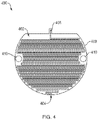
- Nonlimiting examples of embodiments include any number from 2 through 38 changes in direction (as illustrated in FIG. 4 hereinbelow) and any larger numbers of changes in direction as may be required to achieve a desired capacitance in a resonator.
- the lengths of consecutive legs 306 along the path increases along the path from a boundary 310 of the resonator 300 toward an opening 312 through the resonator 300.
- a diameter of the opening 312 is no larger than a width of the gap 304.
- the opening 312 comprises a terminus of the gap 304.
- the opening 312 comprises a semicircular end of the gap 304.
- FIG. 4 schematically illustrates still another embodiment of a loop-gap resonator 400 according to the present invention, wherein an interdigitated capacitor structure 402 and corresponding zig-zag path along a gap 404 is configured to fill the majority of the area of the resonator 400 between an opening 406 and a boundary 408 of the resonator 400, illustrating an exemplary embodiment that maximizes the capacitance of the resonator for a given gap width.
- the length of the legs first increases and then decreases with distance from the opening 406, to maximize use of the available surface area and capacitance of the resonator 400.
- the path follows physical constraints associated with a design of the resonator 400, such as attachment means 410 for mounting the resonator 400 to another structure (not illustrated).
- the resonator 400 is shown to comprise 38 reversals of direction in the zig-zag path.
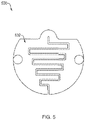
- FIG. 5 schematically illustrates an exemplary embodiment of a loop-gap resonator 500 according to the present invention, including a tapered, interdigitated capacitor structure 502.
- the resonator 500 is approximately 1 cm in diameter and was fabricated from oxygen-free copper using conventional machining methods. In initial tests using a laboratory-made ESR spectrometer, the resonator operated at its design frequency of 1.5 GHz and had a Q (Quality) factor of 600. A similar resonator having a straight path of a prior-art design was found to have a frequency of 4.5 GHz and Q of approximately 1500.
- Loop-gap resonators according to the present invention can provide high radiation fields in resonators smaller in size than the wavelength of the radiation used to interact with a sample contained therein, making them excellent devices for controlling and measuring the quantum state of qubits, which are fundamental building blocks for quantum computing, using pulsed-radiation techniques.
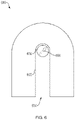
- FIG. 6 schematically illustrates a nanoscale loop-gap resonator 600 according to the present invention, for application to quantum computing.
- the dimensions of the loop-gap resonator 600 are scaled to provide coupling to a single molecular magnet, which would behave as a qubit.
- a resonator according to the present invention would allow the manipulation, control and read-out of the qubit's quantum state.
- the manipulation, control or readout of the qubit's quantum state comprises the application of pulses of electromagnetic radiation to the resonator.
- the resonator 600 is seen to comprise an opening 602 that functionally parallels the opening 406 of the resonator 400 of FIG. 4 . Also illustrated in FIG. 6 is a portion of a gap 604 that functionally parallels the gap 404 illustrated in FIG. 4 . The remainder of the gap 604 is not shown in FIG. 6 , but follows a path functionally similar to the interdigitated, zig-zag pattern of FIG. 4 .
- the opening 602 contains a sample 606 (illustrated as a circle in FIG.
- the sample 606 can be any chemical or molecular species suitable for measurement using spin-resonance spectroscopic techniques, or any quantum object that embodies a qubit, nonlimiting examples of which include single magnetic molecules, quantum dots, and nitrogen vacancy color centers in diamond.
- suitable magnetic species may include Cr 7 M molecular rings, where M can be a transition-metal ion such as Ni, Co, or Mn.
- the quantum object is a superconducting (Josephson) device.
- the opening 602 has a cross sectional dimension in the range of one to 10 nanometers.
- the quantum state 608 is one of an electron spin state, or a nuclear spin state.
- the loop-gap resonator 600 comprises a read-and-control circuit for single or multiple qubits in a quantum computer.
- An exemplary system includes a loop-gap resonator of the present invention, a sample positioned at least partially within an opening of the resonator, a source of a magnetic field that can be applied to the resonator, and a source of electromagnetic radiation having a frequency selected to match a resonance of the loop-gap resonator.
- resonators disclosed herein are illustrated as being cylindrical, or circular and substantially planar in shape, but many other shapes are also possible, including other geometric shapes or more complex shapes selected to optimize resonator performance.
- loop-gap resonators according to the present invention can be fabricated as curved or flexible devices.
- resonators of the present invention have application in nuclear magnetic resonance (NMR) and to other arts that employ high-frequency resonators.
Landscapes
- Physics & Mathematics (AREA)
- General Physics & Mathematics (AREA)
- Condensed Matter Physics & Semiconductors (AREA)
- Engineering & Computer Science (AREA)
- Control Of Motors That Do Not Use Commutators (AREA)
- Theoretical Computer Science (AREA)
- Evolutionary Computation (AREA)
- Data Mining & Analysis (AREA)
- Computational Mathematics (AREA)
- Mathematical Analysis (AREA)
- Mathematical Optimization (AREA)
- Pure & Applied Mathematics (AREA)
- Computing Systems (AREA)
- General Engineering & Computer Science (AREA)
- Mathematical Physics (AREA)
- Software Systems (AREA)
- Artificial Intelligence (AREA)
- Magnetic Resonance Imaging Apparatus (AREA)
- Measurement Of Resistance Or Impedance (AREA)
Claims (12)
- Résonateur (100, 200) destiné au couplage d'un rayonnement électromagnétique à un échantillon à l'échelle d'un objet quantique représentant un bit quantique, le résonateur (100, 200) comprenant : un élément électriquement conducteur ; une ouverture (106, 206) à travers l'élément définissant une boucle d'induction dans l'élément, l'échantillon pouvant être au moins en partie reçu à l'intérieur de l'ouverture (106, 206) ; et un espace allongé (108, 208) dans l'élément définissant un chemin sinueux ayant une longueur entre une frontière de l'élément et l'ouverture, l'espace allongé contribuant à la capacité électrique du résonateur, le chemin sinueux comprenant une pluralité de segments de chemin et de changements de direction entre ceux-ci, et un ou plusieurs des changements de direction comprenant une inversion de direction.
- Résonateur (100, 200) selon la revendication 1 dans lequel l'élément conducteur comprend une couche métallique recouvrant un substrat diélectrique.
- Résonateur (100, 200) selon la revendication 1 dans lequel l'élément conducteur est sensiblement plan.
- Résonateur (100, 200) selon la revendication 1 comprenant en outre un matériau diélectrique recouvrant au moins une partie de l'élément conducteur et/ou remplissant au moins une partie de l'espace (108, 208).
- Résonateur (100, 200) selon la revendication 1 dans lequel la longueur du chemin sinueux est sensiblement proportionnelle à une capacité du résonateur (100, 200) et une largeur de l'espace (108, 208) est sensiblement inversement proportionnelle à une capacité du résonateur (100, 200).
- Résonateur (100, 200) selon la revendication 1 dans lequel une pluralité de segments de chemin adjacents et inversés définissent une structure interdigitée dans l'élément conducteur.
- Résonateur (100, 200) selon la revendication 1 dans lequel le chemin comprend au moins 8 changements de direction.
- Résonateur (100, 200) selon la revendication 1 dans lequel au moins une partie de la longueur de l'espace allongé (108, 208) présente une largeur d'espace inférieure à 10 nanomètres.
- Résonateur (100, 200) selon la revendication 1 dans lequel une dimension transversale la plus grande de l'ouverture n'est pas supérieure à une largeur minimale de l'espace (108, 208).
- Procédé destiné à au moins l'un d'une mesure et d'un changement d'un état quantique d'un échantillon à l'échelle d'un objet quantique représentant un bit quantique, le procédé comprenant les étapes consistant à : positionner au moins une partie de l'échantillon dans une ouverture (106, 206) d'un résonateur à boucle (100, 200) ayant une capacité définie par un espace sinueux (108, 208), délimitant un chemin sinueux, s'étendant entre l'ouverture (106, 206) et un bord externe du résonateur (100, 200) ; exposer simultanément l'échantillon à un champ magnétique et à un rayonnement électromagnétique ; et détecter un signal de résonance provenant de l'échantillon, l'espace allongé (108, 208) contribuant à la capacité électrique du résonateur (100, 200), le chemin sinueux comprenant une pluralité de segments de chemin et de changements de direction entre ceux-ci, et un ou plusieurs des changements de direction comprenant une inversion de direction.
- Procédé selon la revendication 10 dans lequel l'ouverture (106, 206) a une dimension en section transversale inférieure à 10 nanomètres.
- Procédé selon la revendication 10 dans lequel l'échantillon comprend un bit quantique.
Applications Claiming Priority (2)
| Application Number | Priority Date | Filing Date | Title |
|---|---|---|---|
| US201762555127P | 2017-09-07 | 2017-09-07 | |
| PCT/US2018/049649 WO2019051016A1 (fr) | 2017-09-07 | 2018-09-06 | Résonateurs à intervalle de boucle de spectroscopie par résonance de spin |
Publications (3)
| Publication Number | Publication Date |
|---|---|
| EP3679385A1 EP3679385A1 (fr) | 2020-07-15 |
| EP3679385A4 EP3679385A4 (fr) | 2021-06-09 |
| EP3679385B1 true EP3679385B1 (fr) | 2022-10-26 |
Family
ID=65517457
Family Applications (1)
| Application Number | Title | Priority Date | Filing Date |
|---|---|---|---|
| EP18853629.6A Active EP3679385B1 (fr) | 2017-09-07 | 2018-09-06 | Résonateurs à intervalle de boucle de spectroscopie par résonance de spin |
Country Status (5)
| Country | Link |
|---|---|
| US (4) | US11171400B2 (fr) |
| EP (1) | EP3679385B1 (fr) |
| JP (1) | JP7102526B2 (fr) |
| CA (1) | CA3075078C (fr) |
| WO (1) | WO2019051016A1 (fr) |
Cited By (1)
| Publication number | Priority date | Publication date | Assignee | Title |
|---|---|---|---|---|
| US11611137B2 (en) | 2017-09-07 | 2023-03-21 | Amherst College | Loop gap resonators for spin resonance spectroscopy |
Families Citing this family (9)
| Publication number | Priority date | Publication date | Assignee | Title |
|---|---|---|---|---|
| AU2020385023A1 (en) * | 2019-11-15 | 2022-06-30 | Diraq Pty Ltd | Global control for quantum computing systems |
| US11552236B2 (en) * | 2020-01-24 | 2023-01-10 | International Business Machines Corporation | Superconducting qubit capacitance and frequency of operation tuning |
| JP7327808B2 (ja) * | 2020-03-24 | 2023-08-16 | 国立研究開発法人産業技術総合研究所 | 平面ループギャップ共振器、量子センシングシステム及び量子磁気センサーユニット |
| EP4016401B1 (fr) * | 2020-12-21 | 2023-07-05 | Imec VZW | Topologie de commande et de lecture pour bits quantiques spin |
| JP7629813B2 (ja) * | 2021-07-06 | 2025-02-14 | 東京エレクトロン株式会社 | プラズマ処理装置 |
| JP2023148206A (ja) | 2022-03-30 | 2023-10-13 | 日本電気株式会社 | 超伝導量子回路装置 |
| CN114611704B (zh) * | 2022-05-11 | 2022-10-25 | 苏州浪潮智能科技有限公司 | 一种量子比特耦合方法和结构 |
| CN115238900B (zh) * | 2022-06-10 | 2024-11-29 | 华南师范大学 | 一种超导lc原子芯片 |
| CN118841235B (zh) * | 2024-07-11 | 2025-05-06 | 南京大学 | 无线圈式质子型电感器、设计方法及调控方法 |
Family Cites Families (73)
| Publication number | Priority date | Publication date | Assignee | Title |
|---|---|---|---|---|
| US4446429A (en) * | 1981-10-09 | 1984-05-01 | Medical College Of Wisconsin | Microwave resonator |
| US4480239A (en) * | 1983-02-07 | 1984-10-30 | The Medical College Of Wisconsin Inc. | Loop-gap resonator network |
| IT1207069B (it) * | 1986-05-14 | 1989-05-17 | Gte Telecom Spa | Linea di trasmissione a microstriscia per accoppiamento a risonatore dielettrico. |
| US4734647A (en) * | 1987-03-16 | 1988-03-29 | Medical Advances, Inc. | NMR local coil with foil coupling loop |
| US4751464A (en) * | 1987-05-04 | 1988-06-14 | Advanced Nmr Systems, Inc. | Cavity resonator with improved magnetic field uniformity for high frequency operation and reduced dielectric heating in NMR imaging devices |
| GB2222312B (en) * | 1988-08-04 | 1993-05-26 | Matsushita Electric Industrial Co Ltd | A resonator and a filter including the same |
| JPH07333310A (ja) * | 1994-06-10 | 1995-12-22 | Junkosha Co Ltd | ループギャップ共振器及びその組合せ構造 |
| US5821827A (en) * | 1996-12-18 | 1998-10-13 | Endgate Corporation | Coplanar oscillator circuit structures |
| US6255816B1 (en) * | 1998-10-20 | 2001-07-03 | The Ohio State University | Electromagnetic resonator devices and systems incorporating same, resonance and imaging methods |
| US6560567B1 (en) * | 1999-03-03 | 2003-05-06 | Sitaramao S. Yechuri | Method and apparatus for measuring on-wafer lumped capacitances in integrated circuits |
| US6400576B1 (en) * | 1999-04-05 | 2002-06-04 | Sun Microsystems, Inc. | Sub-package bypass capacitor mounting for an array packaged integrated circuit |
| JP3854059B2 (ja) | 1999-11-18 | 2006-12-06 | 株式会社東芝 | 量子情報処理方法および量子情報処理装置 |
| US6313719B1 (en) * | 2000-03-09 | 2001-11-06 | Avaya Technology Corp. | Method of tuning a planar filter with additional coupling created by bent resonator elements |
| US7184555B2 (en) | 2001-04-11 | 2007-02-27 | Magiq Technologies, Inc. | Quantum computation |
| US20030021518A1 (en) | 2001-06-01 | 2003-01-30 | D-Wave Systems, Inc. | Optical transformer device |
| CN1529923A (zh) * | 2001-06-13 | 2004-09-15 | 谐振器和包括相同设备的滤波器 | |
| US6700459B2 (en) * | 2002-05-29 | 2004-03-02 | Superconductor Technologies, Inc. | Dual-mode bandpass filter with direct capacitive couplings and far-field suppression structures |
| US7423427B2 (en) | 2004-05-14 | 2008-09-09 | Massachusetts Institute Of Technology | Arbitrarily accurate composite pulse sequences |
| US7863892B2 (en) | 2005-10-07 | 2011-01-04 | Florida State University Research Foundation | Multiple SQUID magnetometer |
| US7697262B2 (en) * | 2005-10-31 | 2010-04-13 | Avx Corporation | Multilayer ceramic capacitor with internal current cancellation and bottom terminals |
| US8836439B2 (en) * | 2007-10-12 | 2014-09-16 | Los Alamos National Security Llc | Dynamic frequency tuning of electric and magnetic metamaterial response |
| US8222629B2 (en) | 2007-12-07 | 2012-07-17 | Japan Science And Technology Agency | Electronic device using quantum dot |
| US20090147440A1 (en) * | 2007-12-11 | 2009-06-11 | Avx Corporation | Low inductance, high rating capacitor devices |
| US20090295509A1 (en) * | 2008-05-28 | 2009-12-03 | Universal Phase, Inc. | Apparatus and method for reaction of materials using electromagnetic resonators |
| US8315969B2 (en) | 2008-10-10 | 2012-11-20 | Nec Laboratories America, Inc. | Estimating a quantum state of a quantum mechanical system |
| US20100177457A1 (en) * | 2009-01-10 | 2010-07-15 | Simon Edward Willard | Interdigital capacitor with Self-Canceling Inductance |
| US20100188799A1 (en) * | 2009-01-28 | 2010-07-29 | Avx Corporation | Controlled esr low inductance capacitor |
| US8507860B2 (en) * | 2009-05-20 | 2013-08-13 | Nutech Ventures | Terahertz resonator |
| US9040922B2 (en) * | 2009-06-03 | 2015-05-26 | Koninklijke Philips N.V. | THz frequency range antenna |
| US9208445B2 (en) | 2009-11-16 | 2015-12-08 | International Business Machines Corporation | System and method of quantum computing using three-state representation of a qubit |
| US8711897B2 (en) * | 2010-08-11 | 2014-04-29 | Miles Technologies, Llc | Split-ring resonator creating a photonic metamaterial |
| CN103201898B (zh) * | 2011-05-11 | 2015-07-01 | 松下电器产业株式会社 | 电磁共振耦合器 |
| US8642998B2 (en) | 2011-06-14 | 2014-02-04 | International Business Machines Corporation | Array of quantum systems in a cavity for quantum computing |
| CN103620870B (zh) | 2011-06-23 | 2017-02-15 | 加利福尼亚大学董事会 | 小型电气垂直式裂环谐振器天线 |
| US9194922B2 (en) | 2011-10-18 | 2015-11-24 | Technion Research & Development Foundation Limited | System and method for electron spin resonance |
| US9079043B2 (en) * | 2011-11-21 | 2015-07-14 | Thoratec Corporation | Transcutaneous power transmission utilizing non-planar resonators |
| GB201209246D0 (en) * | 2012-05-25 | 2012-07-04 | Imp Innovations Ltd | Structures and materials |
| US8908251B2 (en) * | 2013-01-30 | 2014-12-09 | Hrl Laboratories, Llc | Tunable optical metamaterial |
| US9059305B2 (en) * | 2013-03-04 | 2015-06-16 | International Business Machines Corporation | Planar qubits having increased coherence times |
| EP2965054B1 (fr) * | 2013-03-05 | 2022-07-20 | Teknologian tutkimuskeskus VTT Oy | Détecteur thermique supraconducteur de rayonnement térahertz |
| GB201313601D0 (en) * | 2013-07-30 | 2013-09-11 | Univ Warwick | Sensitive detector |
| WO2015175047A2 (fr) | 2014-02-13 | 2015-11-19 | President And Fellows Of Harvard College | Imagerie par résonance magnétique détectée de manière optique avec un résonateur de champ électromagnétique |
| MX2016015052A (es) * | 2014-05-16 | 2017-04-13 | Plasma Igniter LLC | Diagnostico de ambiente de combustion. |
| FR3033103A1 (fr) * | 2015-02-24 | 2016-08-26 | Univ Paris Diderot Paris 7 | Dispositif resonateur electrique tridimensionnel de type inductance-capacite |
| JP6894378B2 (ja) * | 2015-02-27 | 2021-06-30 | イェール ユニバーシティーYale University | 平面キュービットを非平面共振器に連結するための技術ならびに関連する系および方法 |
| US9891297B2 (en) | 2015-03-13 | 2018-02-13 | President And Fellows Of Harvard College | Magnetic sensing and imaging using interactions between surface electron spins and solid state spins |
| EP3082073B1 (fr) | 2015-04-12 | 2019-01-16 | Hitachi Ltd. | Traitement d'informations quantiques |
| US10381542B2 (en) * | 2015-04-30 | 2019-08-13 | International Business Machines Corporation | Trilayer Josephson junction structure with small air bridge and no interlevel dielectric for superconducting qubits |
| US10355642B2 (en) * | 2015-05-27 | 2019-07-16 | Silicon Laboratories Inc. | Comb terminals for planar integrated circuit inductor |
| AU2016267410B2 (en) | 2015-05-28 | 2021-04-01 | Newsouth Innovations Pty Limited | A quantum processing apparatus and a method of operating a quantum processing apparatus |
| AU2016287781B2 (en) | 2015-06-30 | 2022-01-13 | The University Of Melbourne | Determining a spatial configuration of multiple nuclei |
| US9443810B1 (en) * | 2015-09-14 | 2016-09-13 | Qualcomm Incorporated | Flip-chip employing integrated cavity filter, and related components, systems, and methods |
| US9589236B1 (en) * | 2015-09-28 | 2017-03-07 | International Business Machines Corporation | High fidelity and high efficiency qubit readout scheme |
| US9454061B1 (en) * | 2015-12-17 | 2016-09-27 | International Business Machines Corporation | Quantum coherent microwave to optical conversion scheme employing a mechanical element and a squid |
| FR3046701B1 (fr) * | 2016-01-08 | 2018-03-23 | Commissariat A L'energie Atomique Et Aux Energies Alternatives | Antenne reseau, en particulier pour imagerie par resonance magnetique nucleaire, comprenant des resonateurs electromagnetiques lineaires et au moins un dispositif de decouplage |
| FI126944B (en) * | 2016-01-27 | 2017-08-15 | Stealthcase Oy | Apparatus and method for receiving and further emitting electromagnetic signals |
| US10381704B2 (en) * | 2016-02-16 | 2019-08-13 | GM Global Technology Operations LLC | Embedded broadband glass coplanar waveguide coupler |
| US9972587B2 (en) * | 2016-03-02 | 2018-05-15 | Panasonic Intellectual Property Management Co., Ltd. | Signal transmission device using electromagnetic resonance coupler |
| US10740688B2 (en) * | 2016-03-11 | 2020-08-11 | Rigetti & Co, Inc. | Impedance-matched microwave quantum circuit systems |
| EP3220113B1 (fr) * | 2016-03-16 | 2019-05-01 | Centre National de la Recherche Scientifique - CNRS - | Transducteur optomécanique pour ondes électromagnétiques en térahertz |
| WO2017189950A1 (fr) * | 2016-04-29 | 2017-11-02 | Commscope Technologies Llc | Condensateurs à microruban avec structures de résonateur complémentaires |
| CN107369667A (zh) * | 2016-05-13 | 2017-11-21 | 松下电器产业株式会社 | 信号传送装置 |
| CN108074789B (zh) * | 2016-11-15 | 2019-10-11 | 北京北方华创微电子装备有限公司 | 一种微波传输装置和半导体处理设备 |
| WO2018182571A1 (fr) * | 2017-03-28 | 2018-10-04 | Intel Corporation | Lignes de polarisation de flux de courant commandé dans des dispositifs à bits quantiques |
| US11283296B2 (en) * | 2017-05-26 | 2022-03-22 | Nucurrent, Inc. | Crossover inductor coil and assembly for wireless transmission |
| EP3679385B1 (fr) | 2017-09-07 | 2022-10-26 | Amherst College | Résonateurs à intervalle de boucle de spectroscopie par résonance de spin |
| US20190094306A1 (en) * | 2017-09-25 | 2019-03-28 | Fujitsu Limited | Battery's residual energy measurement circuit and sensor node |
| US20190186456A1 (en) * | 2017-12-20 | 2019-06-20 | Plasma Igniter, LLC | Magnetic Direction of a Plasma Corona Provided Proximate to a Resonator |
| US10847705B2 (en) * | 2018-02-15 | 2020-11-24 | Intel Corporation | Reducing crosstalk from flux bias lines in qubit devices |
| US10468578B2 (en) * | 2018-02-20 | 2019-11-05 | Intel Corporation | Package substrates with top superconductor layers for qubit devices |
| US11177912B2 (en) * | 2018-03-06 | 2021-11-16 | Intel Corporation | Quantum circuit assemblies with on-chip demultiplexers |
| US11552030B2 (en) * | 2018-07-31 | 2023-01-10 | Intel Corporation | High frequency capacitor with inductance cancellation |
| IT201900016193A1 (it) * | 2019-09-12 | 2021-03-12 | St Microelectronics Srl | Dispositivo di potenza, sistema includente il dispositivo di potenza, metodo di fabbricazione del dispositivo di potenza e metodo di controllo del dispositivo di potenza |
-
2018
- 2018-09-06 EP EP18853629.6A patent/EP3679385B1/fr active Active
- 2018-09-06 US US16/123,029 patent/US11171400B2/en active Active
- 2018-09-06 JP JP2020536491A patent/JP7102526B2/ja active Active
- 2018-09-06 WO PCT/US2018/049649 patent/WO2019051016A1/fr not_active Ceased
- 2018-09-06 CA CA3075078A patent/CA3075078C/fr active Active
-
2021
- 2021-10-29 US US17/514,188 patent/US11611137B2/en active Active
-
2023
- 2023-03-08 US US18/118,973 patent/US20230246321A1/en not_active Abandoned
-
2024
- 2024-02-28 US US18/590,510 patent/US20240204385A1/en not_active Abandoned
Cited By (1)
| Publication number | Priority date | Publication date | Assignee | Title |
|---|---|---|---|---|
| US11611137B2 (en) | 2017-09-07 | 2023-03-21 | Amherst College | Loop gap resonators for spin resonance spectroscopy |
Also Published As
| Publication number | Publication date |
|---|---|
| US20220052431A1 (en) | 2022-02-17 |
| US20190074570A1 (en) | 2019-03-07 |
| CA3075078A1 (fr) | 2019-03-14 |
| JP2021501899A (ja) | 2021-01-21 |
| WO2019051016A1 (fr) | 2019-03-14 |
| EP3679385A1 (fr) | 2020-07-15 |
| US20240204385A1 (en) | 2024-06-20 |
| EP3679385A4 (fr) | 2021-06-09 |
| JP7102526B2 (ja) | 2022-07-19 |
| US20230246321A1 (en) | 2023-08-03 |
| US11171400B2 (en) | 2021-11-09 |
| CA3075078C (fr) | 2023-02-14 |
| US11611137B2 (en) | 2023-03-21 |
Similar Documents
| Publication | Publication Date | Title |
|---|---|---|
| US11611137B2 (en) | Loop gap resonators for spin resonance spectroscopy | |
| US6445271B1 (en) | Three-dimensional micro-coils in planar substrates | |
| US6498557B2 (en) | Three-dimensional micro-coils in planar substrates | |
| US4446429A (en) | Microwave resonator | |
| Bart et al. | Optimization of stripline-based microfluidic chips for high-resolution NMR | |
| US4504788A (en) | Enclosed loop-gap resonator | |
| EP2951602B1 (fr) | Dispositif de résonance pour résonance de spin électronique | |
| EP2875369B1 (fr) | Résonateurs à boucles croisées | |
| US7216054B1 (en) | Electromagnetic method and apparatus for the measurement of linear position | |
| JPS59138101A (ja) | 空胴共振器 | |
| JP2021501899A5 (fr) | ||
| KT et al. | Dual band RF sensor for testing of magnetic properties of materials using meandered line SRR | |
| US7088101B2 (en) | Aqueous sample holder for EPR and MR spectroscopy | |
| Lee et al. | Negative interresonator coupling structure enclosed in waveguide resonator filter | |
| Noori et al. | Microwave filters based on novel dielectric split‐ring resonators with high unloaded quality factors | |
| Borthakur et al. | Octagonal nested CSRR sensor for improved liquid permittivity sensing | |
| Tiwari et al. | Metamaterial inspired contactless angular displacement sensor with wide dynamic range and bandwidth | |
| US7592811B2 (en) | High-frequency resonant cavity for nuclear magnetic resonance, using radio-frequency transmission lines | |
| Gamouh et al. | Microwave biosensor based on a double metamaterial particle | |
| RU2824304C1 (ru) | Антенна | |
| Elfeshawy et al. | Biconical Cavity Utilised in Realising Quadruple‐and Quintuple‐Mode Wideband Bandpass Filters | |
| RU2466414C1 (ru) | Петлевой резонатор | |
| Botes et al. | Spatially decoupled varactor biasing for a tunable staircase filter | |
| JP5118319B2 (ja) | 空洞共振器、及びそれを用いた電子スピン共鳴測定装置 | |
| Xiao et al. | High-Sensitivity Microwave Sensor Based on Slot Structures for Permittivity Characterization |
Legal Events
| Date | Code | Title | Description |
|---|---|---|---|
| STAA | Information on the status of an ep patent application or granted ep patent |
Free format text: STATUS: THE INTERNATIONAL PUBLICATION HAS BEEN MADE |
|
| PUAI | Public reference made under article 153(3) epc to a published international application that has entered the european phase |
Free format text: ORIGINAL CODE: 0009012 |
|
| STAA | Information on the status of an ep patent application or granted ep patent |
Free format text: STATUS: REQUEST FOR EXAMINATION WAS MADE |
|
| 17P | Request for examination filed |
Effective date: 20200227 |
|
| AK | Designated contracting states |
Kind code of ref document: A1 Designated state(s): AL AT BE BG CH CY CZ DE DK EE ES FI FR GB GR HR HU IE IS IT LI LT LU LV MC MK MT NL NO PL PT RO RS SE SI SK SM TR |
|
| AX | Request for extension of the european patent |
Extension state: BA ME |
|
| DAV | Request for validation of the european patent (deleted) | ||
| DAX | Request for extension of the european patent (deleted) | ||
| A4 | Supplementary search report drawn up and despatched |
Effective date: 20210510 |
|
| RIC1 | Information provided on ipc code assigned before grant |
Ipc: G01R 33/343 20060101AFI20210503BHEP Ipc: G01R 33/60 20060101ALN20210503BHEP Ipc: G01N 24/10 20060101ALN20210503BHEP Ipc: H01P 7/08 20060101ALN20210503BHEP |
|
| GRAP | Despatch of communication of intention to grant a patent |
Free format text: ORIGINAL CODE: EPIDOSNIGR1 |
|
| STAA | Information on the status of an ep patent application or granted ep patent |
Free format text: STATUS: GRANT OF PATENT IS INTENDED |
|
| RIC1 | Information provided on ipc code assigned before grant |
Ipc: H01P 7/08 20060101ALN20220303BHEP Ipc: G01N 24/10 20060101ALN20220303BHEP Ipc: G01R 33/60 20060101ALN20220303BHEP Ipc: G01R 33/343 20060101AFI20220303BHEP |
|
| RIC1 | Information provided on ipc code assigned before grant |
Ipc: H01P 7/08 20060101ALN20220315BHEP Ipc: G01N 24/10 20060101ALN20220315BHEP Ipc: G01R 33/60 20060101ALN20220315BHEP Ipc: G01R 33/343 20060101AFI20220315BHEP |
|
| INTG | Intention to grant announced |
Effective date: 20220331 |
|
| GRAS | Grant fee paid |
Free format text: ORIGINAL CODE: EPIDOSNIGR3 |
|
| GRAA | (expected) grant |
Free format text: ORIGINAL CODE: 0009210 |
|
| STAA | Information on the status of an ep patent application or granted ep patent |
Free format text: STATUS: THE PATENT HAS BEEN GRANTED |
|
| AK | Designated contracting states |
Kind code of ref document: B1 Designated state(s): AL AT BE BG CH CY CZ DE DK EE ES FI FR GB GR HR HU IE IS IT LI LT LU LV MC MK MT NL NO PL PT RO RS SE SI SK SM TR |
|
| REG | Reference to a national code |
Ref country code: GB Ref legal event code: FG4D |
|
| REG | Reference to a national code |
Ref country code: CH Ref legal event code: EP |
|
| REG | Reference to a national code |
Ref country code: AT Ref legal event code: REF Ref document number: 1527404 Country of ref document: AT Kind code of ref document: T Effective date: 20221115 |
|
| REG | Reference to a national code |
Ref country code: DE Ref legal event code: R096 Ref document number: 602018042382 Country of ref document: DE |
|
| REG | Reference to a national code |
Ref country code: IE Ref legal event code: FG4D |
|
| REG | Reference to a national code |
Ref country code: NL Ref legal event code: FP |
|
| REG | Reference to a national code |
Ref country code: LT Ref legal event code: MG9D |
|
| PG25 | Lapsed in a contracting state [announced via postgrant information from national office to epo] |
Ref country code: SE Free format text: LAPSE BECAUSE OF FAILURE TO SUBMIT A TRANSLATION OF THE DESCRIPTION OR TO PAY THE FEE WITHIN THE PRESCRIBED TIME-LIMIT Effective date: 20221026 Ref country code: PT Free format text: LAPSE BECAUSE OF FAILURE TO SUBMIT A TRANSLATION OF THE DESCRIPTION OR TO PAY THE FEE WITHIN THE PRESCRIBED TIME-LIMIT Effective date: 20230227 Ref country code: NO Free format text: LAPSE BECAUSE OF FAILURE TO SUBMIT A TRANSLATION OF THE DESCRIPTION OR TO PAY THE FEE WITHIN THE PRESCRIBED TIME-LIMIT Effective date: 20230126 Ref country code: LT Free format text: LAPSE BECAUSE OF FAILURE TO SUBMIT A TRANSLATION OF THE DESCRIPTION OR TO PAY THE FEE WITHIN THE PRESCRIBED TIME-LIMIT Effective date: 20221026 Ref country code: FI Free format text: LAPSE BECAUSE OF FAILURE TO SUBMIT A TRANSLATION OF THE DESCRIPTION OR TO PAY THE FEE WITHIN THE PRESCRIBED TIME-LIMIT Effective date: 20221026 Ref country code: ES Free format text: LAPSE BECAUSE OF FAILURE TO SUBMIT A TRANSLATION OF THE DESCRIPTION OR TO PAY THE FEE WITHIN THE PRESCRIBED TIME-LIMIT Effective date: 20221026 |
|
| PG25 | Lapsed in a contracting state [announced via postgrant information from national office to epo] |
Ref country code: RS Free format text: LAPSE BECAUSE OF FAILURE TO SUBMIT A TRANSLATION OF THE DESCRIPTION OR TO PAY THE FEE WITHIN THE PRESCRIBED TIME-LIMIT Effective date: 20221026 Ref country code: PL Free format text: LAPSE BECAUSE OF FAILURE TO SUBMIT A TRANSLATION OF THE DESCRIPTION OR TO PAY THE FEE WITHIN THE PRESCRIBED TIME-LIMIT Effective date: 20221026 Ref country code: LV Free format text: LAPSE BECAUSE OF FAILURE TO SUBMIT A TRANSLATION OF THE DESCRIPTION OR TO PAY THE FEE WITHIN THE PRESCRIBED TIME-LIMIT Effective date: 20221026 Ref country code: IS Free format text: LAPSE BECAUSE OF FAILURE TO SUBMIT A TRANSLATION OF THE DESCRIPTION OR TO PAY THE FEE WITHIN THE PRESCRIBED TIME-LIMIT Effective date: 20230226 Ref country code: HR Free format text: LAPSE BECAUSE OF FAILURE TO SUBMIT A TRANSLATION OF THE DESCRIPTION OR TO PAY THE FEE WITHIN THE PRESCRIBED TIME-LIMIT Effective date: 20221026 Ref country code: GR Free format text: LAPSE BECAUSE OF FAILURE TO SUBMIT A TRANSLATION OF THE DESCRIPTION OR TO PAY THE FEE WITHIN THE PRESCRIBED TIME-LIMIT Effective date: 20230127 |
|
| REG | Reference to a national code |
Ref country code: DE Ref legal event code: R097 Ref document number: 602018042382 Country of ref document: DE |
|
| PG25 | Lapsed in a contracting state [announced via postgrant information from national office to epo] |
Ref country code: SM Free format text: LAPSE BECAUSE OF FAILURE TO SUBMIT A TRANSLATION OF THE DESCRIPTION OR TO PAY THE FEE WITHIN THE PRESCRIBED TIME-LIMIT Effective date: 20221026 Ref country code: RO Free format text: LAPSE BECAUSE OF FAILURE TO SUBMIT A TRANSLATION OF THE DESCRIPTION OR TO PAY THE FEE WITHIN THE PRESCRIBED TIME-LIMIT Effective date: 20221026 Ref country code: EE Free format text: LAPSE BECAUSE OF FAILURE TO SUBMIT A TRANSLATION OF THE DESCRIPTION OR TO PAY THE FEE WITHIN THE PRESCRIBED TIME-LIMIT Effective date: 20221026 Ref country code: DK Free format text: LAPSE BECAUSE OF FAILURE TO SUBMIT A TRANSLATION OF THE DESCRIPTION OR TO PAY THE FEE WITHIN THE PRESCRIBED TIME-LIMIT Effective date: 20221026 Ref country code: CZ Free format text: LAPSE BECAUSE OF FAILURE TO SUBMIT A TRANSLATION OF THE DESCRIPTION OR TO PAY THE FEE WITHIN THE PRESCRIBED TIME-LIMIT Effective date: 20221026 |
|
| PG25 | Lapsed in a contracting state [announced via postgrant information from national office to epo] |
Ref country code: SK Free format text: LAPSE BECAUSE OF FAILURE TO SUBMIT A TRANSLATION OF THE DESCRIPTION OR TO PAY THE FEE WITHIN THE PRESCRIBED TIME-LIMIT Effective date: 20221026 Ref country code: AL Free format text: LAPSE BECAUSE OF FAILURE TO SUBMIT A TRANSLATION OF THE DESCRIPTION OR TO PAY THE FEE WITHIN THE PRESCRIBED TIME-LIMIT Effective date: 20221026 |
|
| PLBE | No opposition filed within time limit |
Free format text: ORIGINAL CODE: 0009261 |
|
| STAA | Information on the status of an ep patent application or granted ep patent |
Free format text: STATUS: NO OPPOSITION FILED WITHIN TIME LIMIT |
|
| 26N | No opposition filed |
Effective date: 20230727 |
|
| REG | Reference to a national code |
Ref country code: AT Ref legal event code: UEP Ref document number: 1527404 Country of ref document: AT Kind code of ref document: T Effective date: 20221026 |
|
| PG25 | Lapsed in a contracting state [announced via postgrant information from national office to epo] |
Ref country code: SI Free format text: LAPSE BECAUSE OF FAILURE TO SUBMIT A TRANSLATION OF THE DESCRIPTION OR TO PAY THE FEE WITHIN THE PRESCRIBED TIME-LIMIT Effective date: 20221026 |
|
| PG25 | Lapsed in a contracting state [announced via postgrant information from national office to epo] |
Ref country code: LU Free format text: LAPSE BECAUSE OF NON-PAYMENT OF DUE FEES Effective date: 20230906 |
|
| PG25 | Lapsed in a contracting state [announced via postgrant information from national office to epo] |
Ref country code: LU Free format text: LAPSE BECAUSE OF NON-PAYMENT OF DUE FEES Effective date: 20230906 Ref country code: IT Free format text: LAPSE BECAUSE OF FAILURE TO SUBMIT A TRANSLATION OF THE DESCRIPTION OR TO PAY THE FEE WITHIN THE PRESCRIBED TIME-LIMIT Effective date: 20221026 Ref country code: MC Free format text: LAPSE BECAUSE OF FAILURE TO SUBMIT A TRANSLATION OF THE DESCRIPTION OR TO PAY THE FEE WITHIN THE PRESCRIBED TIME-LIMIT Effective date: 20221026 |
|
| PG25 | Lapsed in a contracting state [announced via postgrant information from national office to epo] |
Ref country code: BG Free format text: LAPSE BECAUSE OF FAILURE TO SUBMIT A TRANSLATION OF THE DESCRIPTION OR TO PAY THE FEE WITHIN THE PRESCRIBED TIME-LIMIT Effective date: 20221026 |
|
| PG25 | Lapsed in a contracting state [announced via postgrant information from national office to epo] |
Ref country code: BG Free format text: LAPSE BECAUSE OF FAILURE TO SUBMIT A TRANSLATION OF THE DESCRIPTION OR TO PAY THE FEE WITHIN THE PRESCRIBED TIME-LIMIT Effective date: 20221026 |
|
| PG25 | Lapsed in a contracting state [announced via postgrant information from national office to epo] |
Ref country code: CY Free format text: LAPSE BECAUSE OF FAILURE TO SUBMIT A TRANSLATION OF THE DESCRIPTION OR TO PAY THE FEE WITHIN THE PRESCRIBED TIME-LIMIT; INVALID AB INITIO Effective date: 20180906 |
|
| PG25 | Lapsed in a contracting state [announced via postgrant information from national office to epo] |
Ref country code: HU Free format text: LAPSE BECAUSE OF FAILURE TO SUBMIT A TRANSLATION OF THE DESCRIPTION OR TO PAY THE FEE WITHIN THE PRESCRIBED TIME-LIMIT; INVALID AB INITIO Effective date: 20180906 |
|
| PGFP | Annual fee paid to national office [announced via postgrant information from national office to epo] |
Ref country code: NL Payment date: 20250805 Year of fee payment: 8 |
|
| REG | Reference to a national code |
Ref country code: CH Ref legal event code: U11 Free format text: ST27 STATUS EVENT CODE: U-0-0-U10-U11 (AS PROVIDED BY THE NATIONAL OFFICE) Effective date: 20251001 |
|
| PGFP | Annual fee paid to national office [announced via postgrant information from national office to epo] |
Ref country code: DE Payment date: 20250806 Year of fee payment: 8 |
|
| PGFP | Annual fee paid to national office [announced via postgrant information from national office to epo] |
Ref country code: BE Payment date: 20250805 Year of fee payment: 8 Ref country code: GB Payment date: 20250805 Year of fee payment: 8 |
|
| PGFP | Annual fee paid to national office [announced via postgrant information from national office to epo] |
Ref country code: AT Payment date: 20250806 Year of fee payment: 8 Ref country code: FR Payment date: 20250807 Year of fee payment: 8 |
|
| PGFP | Annual fee paid to national office [announced via postgrant information from national office to epo] |
Ref country code: IE Payment date: 20250805 Year of fee payment: 8 |
|
| PG25 | Lapsed in a contracting state [announced via postgrant information from national office to epo] |
Ref country code: TR Free format text: LAPSE BECAUSE OF FAILURE TO SUBMIT A TRANSLATION OF THE DESCRIPTION OR TO PAY THE FEE WITHIN THE PRESCRIBED TIME-LIMIT Effective date: 20221026 |
|
| PGFP | Annual fee paid to national office [announced via postgrant information from national office to epo] |
Ref country code: CH Payment date: 20251001 Year of fee payment: 8 |