EP3679768B1 - Système gradateur de lumière - Google Patents
Système gradateur de lumière Download PDFInfo
- Publication number
- EP3679768B1 EP3679768B1 EP18759865.1A EP18759865A EP3679768B1 EP 3679768 B1 EP3679768 B1 EP 3679768B1 EP 18759865 A EP18759865 A EP 18759865A EP 3679768 B1 EP3679768 B1 EP 3679768B1
- Authority
- EP
- European Patent Office
- Prior art keywords
- dimming
- channel
- temperature
- channels
- dimmer system
- Prior art date
- Legal status (The legal status is an assumption and is not a legal conclusion. Google has not performed a legal analysis and makes no representation as to the accuracy of the status listed.)
- Active
Links
Images

Classifications
-
- H—ELECTRICITY
- H05—ELECTRIC TECHNIQUES NOT OTHERWISE PROVIDED FOR
- H05B—ELECTRIC HEATING; ELECTRIC LIGHT SOURCES NOT OTHERWISE PROVIDED FOR; CIRCUIT ARRANGEMENTS FOR ELECTRIC LIGHT SOURCES, IN GENERAL
- H05B39/00—Circuit arrangements or apparatus for operating incandescent light sources
- H05B39/04—Controlling
- H05B39/041—Controlling the light-intensity of the source
- H05B39/044—Controlling the light-intensity of the source continuously
- H05B39/048—Controlling the light-intensity of the source continuously with reverse phase control
-
- H—ELECTRICITY
- H05—ELECTRIC TECHNIQUES NOT OTHERWISE PROVIDED FOR
- H05B—ELECTRIC HEATING; ELECTRIC LIGHT SOURCES NOT OTHERWISE PROVIDED FOR; CIRCUIT ARRANGEMENTS FOR ELECTRIC LIGHT SOURCES, IN GENERAL
- H05B39/00—Circuit arrangements or apparatus for operating incandescent light sources
- H05B39/04—Controlling
-
- H—ELECTRICITY
- H05—ELECTRIC TECHNIQUES NOT OTHERWISE PROVIDED FOR
- H05B—ELECTRIC HEATING; ELECTRIC LIGHT SOURCES NOT OTHERWISE PROVIDED FOR; CIRCUIT ARRANGEMENTS FOR ELECTRIC LIGHT SOURCES, IN GENERAL
- H05B39/00—Circuit arrangements or apparatus for operating incandescent light sources
- H05B39/04—Controlling
- H05B39/041—Controlling the light-intensity of the source
- H05B39/044—Controlling the light-intensity of the source continuously
-
- H—ELECTRICITY
- H05—ELECTRIC TECHNIQUES NOT OTHERWISE PROVIDED FOR
- H05B—ELECTRIC HEATING; ELECTRIC LIGHT SOURCES NOT OTHERWISE PROVIDED FOR; CIRCUIT ARRANGEMENTS FOR ELECTRIC LIGHT SOURCES, IN GENERAL
- H05B44/00—Circuit arrangements for operating electroluminescent light sources
-
- H—ELECTRICITY
- H05—ELECTRIC TECHNIQUES NOT OTHERWISE PROVIDED FOR
- H05B—ELECTRIC HEATING; ELECTRIC LIGHT SOURCES NOT OTHERWISE PROVIDED FOR; CIRCUIT ARRANGEMENTS FOR ELECTRIC LIGHT SOURCES, IN GENERAL
- H05B45/00—Circuit arrangements for operating light-emitting diodes [LED]
- H05B45/10—Controlling the intensity of the light
- H05B45/18—Controlling the intensity of the light using temperature feedback
-
- H—ELECTRICITY
- H05—ELECTRIC TECHNIQUES NOT OTHERWISE PROVIDED FOR
- H05B—ELECTRIC HEATING; ELECTRIC LIGHT SOURCES NOT OTHERWISE PROVIDED FOR; CIRCUIT ARRANGEMENTS FOR ELECTRIC LIGHT SOURCES, IN GENERAL
- H05B45/00—Circuit arrangements for operating light-emitting diodes [LED]
- H05B45/50—Circuit arrangements for operating light-emitting diodes [LED] responsive to malfunctions or undesirable behaviour of LEDs; responsive to LED life; Protective circuits
- H05B45/56—Circuit arrangements for operating light-emitting diodes [LED] responsive to malfunctions or undesirable behaviour of LEDs; responsive to LED life; Protective circuits involving measures to prevent abnormal temperature of the LEDs
-
- Y—GENERAL TAGGING OF NEW TECHNOLOGICAL DEVELOPMENTS; GENERAL TAGGING OF CROSS-SECTIONAL TECHNOLOGIES SPANNING OVER SEVERAL SECTIONS OF THE IPC; TECHNICAL SUBJECTS COVERED BY FORMER USPC CROSS-REFERENCE ART COLLECTIONS [XRACs] AND DIGESTS
- Y02—TECHNOLOGIES OR APPLICATIONS FOR MITIGATION OR ADAPTATION AGAINST CLIMATE CHANGE
- Y02B—CLIMATE CHANGE MITIGATION TECHNOLOGIES RELATED TO BUILDINGS, e.g. HOUSING, HOUSE APPLIANCES OR RELATED END-USER APPLICATIONS
- Y02B20/00—Energy efficient lighting technologies, e.g. halogen lamps or gas discharge lamps
Definitions
- the invention relates to a dimmer system for controlling the power consumption of a load that can be connected to a dimmer system, in particular an LED light, the dimmer system comprising at least two galvanically isolated dimming channels connected in parallel.
- the invention also relates to a method for controlling the power consumption of a load that can be connected to a dimmer system.
- Dimmers or dimming devices or dimmer systems for brightness control are generally known and they are used to vary the output of a lighting device. Such a variation in performance can take place by means of phase control or phase control.
- phase control the current is switched on with a delay after the alternating voltage has passed zero and flows until the next current zero crossing.
- phase control on the other hand, the current is switched on immediately after the zero crossing and switched off again before the next zero crossing.
- German patent specification DE102016209278B3 discloses a dimmer system for controlling the power consumption of a connectable load, with a master control device and at least two slave dimmers, the master control device emitting synchronization signals for synchronizing the respective outputs of the slave dimmers via a suitable communication link to the respective slave dimmers ; in which each slave dimmer has a slave controller which receives the synchronization signals from the master controller; wherein the slave dimmers are connected in parallel to provide a common controlled output for the connectable load; wherein the master controller sends the synchronization signal to the slave controllers at the same time; each slave control device being set up to measure the time between the received synchronization signal and the respectively detected mains voltage zero crossing and to report this time to the master control device; wherein the master control device is set up to determine a respective correction value from the time difference between the respective reported time differences for the slave control devices and is set up to send the respective correction values to the respective slave control devices via the communication link to correct the control of the output output by the respective slave slave
- multi-channel dimmer systems are known in which a master dimmer has several power levels (slave dimmers, channels) that can be connected in parallel on the output side to increase power. With these powerful dimmers, several physical channels (slaves) are switched in parallel and a powerful logical channel is created. With this parallel connection it is very important that the outputs switch at the same time. If two channels are switched in parallel and the 2nd channel switches too late (with phase control) or too early (with phase control), the first channel is overloaded. This leads to excessive heating and then to derating or switching off the logical channel, in which case both physical channels are affected. A Any device replacement that may be necessary causes costs and disruptions for the customer.
- a dimmer system for controlling the power consumption of a load that can be connected, in particular an LED light, with at least two galvanically isolated dimming channels connected in parallel, each dimming channel comprising a device for monitoring the temperature of its switching elements, and each dimming channel having a control unit for shifting its Dimming edge, based on the temperature of its switching elements, includes in order to distribute the power loss of the connected load essentially evenly over the dimming channels. This improves the dimmability of large loads in parallel operation.
- the number of channels that can be connected in parallel increases, which in turn means that even larger loads can be supported. This makes the dimmer system more versatile. It is thus possible to provide a scalable dimmer system depending on the particular requirements placed on the lighting system and the load required for this.
- the dimmer system advantageously has connection terminals for coupling to an installation bus (e.g. KNX bus system).
- a first advantageous embodiment of the invention is that the control unit of the respective dimming channel shifts the respective dimming edge of the respective dimming channel forward or backward in time as a function of the temperature of the respective switching elements.
- Each dimming channel has for this purpose a device (eg a temperature sensor that provides an electrical signal as a function of the detected temperature) with which it is able to monitor the temperature of its switching elements. If the temperature at the switching element increases, it can be assumed that the channel switches on too early (phase control mode) or switches off too late (phase control mode). The control unit then advances the dimming edge in suitable steps (phase section) or backwards (phase control operation) until the temperature at the switching element no longer rises as quickly, stagnates or even drops, depending on the temperature range in which you are.
- a further advantageous embodiment of the invention is that the time shift of the respective dimming edge forwards or backwards takes place until the gradient of the temperature of the respective switching elements decreases.
- the temperature gradient is a measure of the intensity or strength of the temperature change. The temperature gradient thus indicates whether a dimming edge shift is successful or will be successful.
- a further advantageous embodiment of the invention is that the time shift of the respective dimming edge forwards or backwards takes place until the temperature of the respective switching elements stagnates.
- a stagnation of the temperature of the respective switching elements is an indication that the time shift of the respective dimming edge is successful, because there is no more temperature increase.
- a further advantageous embodiment of the invention is that the time shifting of the respective dimming edge forwards or backwards takes place until it is the temperature of the respective switching elements is reduced. A reduction in the temperature of the respective switching elements is also an indication that the time shifting of the respective dimming edge is successful.
- the dimmer system comprises a master control unit which is connected in terms of data technology to the control units of the dimming channels, the master control unit prescribing a setpoint value to the control units of the dimming channels, the respective shift of the dimming edges being based on the setpoint value.
- the parallel, galvanically isolated dimming channels each have their own circuits for phase synchronization.
- temporal differences can arise in the zero crossing detection. These time differences then lead to non-synchronous switching of the dimming channels.
- the dimming channels or the respective control units of the dimming channels are advantageously controlled by a master control unit of the dimmer system.
- the master control unit knows the temperature values in the respective dimming channels and determines appropriate setpoint values for the phase shift based on the temperature values.
- the master control unit advantageously specifies a dedicated setpoint for a respective dimming channel.
- the setpoint value is based on the temperature of the switching elements built into the dimmer system.
- the temperature of the built-in switching elements can be easily determined, e.g. using semiconductor temperature sensors or thermistors (NTC, PTC).
- Another advantageous embodiment of the invention is that the dimming channels on a common coolant or heat sink, in particular a cooling plate, are arranged.
- the cooling capacity of the coolant or heat sink common to all dimming channels can be used flexibly to dissipate or dissipate the heat loss of the dimming channels used in each case.
- the number of dimming channels used can thus be scaled with a common coolant or heat sink.
- the object is also achieved by a method for controlling the power consumption of a load that can be connected to a dimmer system, in particular an LED light, the dimmer system comprising at least two parallel-connected, galvanically isolated dimming channels, based on the temperature of the switching elements of the respective dimming channel Dimming edge of the respective dimming channel takes place in order to distribute the power loss of the connected load essentially evenly over the dimming channels.
- the method according to the invention enables a simple type of uniform distribution of the power loss of a connected load to the dimming channels used in a dimmer system.
- the temperature of the switching elements can be determined e.g. by digital temperature sensors or semiconductor sensors.
- a further advantageous embodiment of the invention is that, depending on the temperature of the respective switching elements, the respective dimming edge of the respective dimming channel is shifted forwards or backwards in time. This synchronizes the dimming channels. In particular, the respective dimming channel-specific zero crossings are synchronized.
- LED technology is on the advance in the market for lighting, which means that the performance requirements for dimming channels have decreased.
- An attempt is made to accommodate several channels in the same size, which support less power but thereby provide greater flexibility and are optimized for LED lamps.
- a load with greater power e.g. chandelier with lightbulbs
- several channels can be connected in parallel to form a more powerful logical channel for this purpose.
- the load current is divided between the channels connected in parallel and the power loss is thus evenly distributed.
- Dimmers or dimming devices are used to vary the output of a lighting device. Such a variation in performance can take place by means of phase control or phase control.
- phase control the current is switched on with a delay after the AC voltage has crossed zero and flows until the next zero crossing.
- phase control on the other hand, the current is switched on immediately after the zero crossing and switched off again before the next zero crossing.
- Triacs switch bidirectionally and cancel when the current crosses zero.
- the input voltage of the lighting device e.g. LED lamp
- the input voltage of the lighting device e.g. LED lamp
- LED lamps as lighting devices can therefore be dimmed by means of phase control or phase control.
- phase control or phase control With so-called universal dimmers, both the phase control and the phase control for dimming such dimmable LED lamps (LED chip plus ballast) are possible.
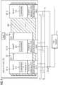
- Figure 1 shows an exemplary arrangement for a dimmer system DS (e.g. a universal dimmer) for controlling the power consumption of a connectable load L (e.g. a lighting device), in particular an LED light, with at least two parallel-connected, galvanically isolated dimming channels DK_A, DK_B, DK_X, where each dimming channel DK_A, DK_B, DK_X includes a device for temperature monitoring TS1 - TS3 of its switching elements (e.g. components, transistors, cables), and each dimming channel DK_A, DK_B, DK_X has a control unit SE1 - SE3 for shifting its dimming edge, based on the temperature T.
- a dimmer system DS e.g. a universal dimmer
- a connectable load L e.g. a lighting device
- a connectable load L e.g. a lighting device
- a connectable load L e.g. a
- the dimming channels DK_A, DK_B, DK_X are galvanically separated from each other (GT) or galvanically decoupled.
- the temperature can be monitored, for example, by means of semiconductor temperature sensors.
- a control unit SE1 - SE3 of a dimming channel DK_A, DK_B, DK_X is advantageously designed to determine a current zero passage for phase control or phase control (e.g. on the basis of the measured voltage).
- a control unit SE1 - SE3 is advantageously implemented using an integrated circuit (e.g. IC, microchip).
- T Temperature
- the respective switching elements e.g. components, circuits, connections
- the respective dimming edge of the respective dimming channel DK_A, DK_B, DK_X shifted forwards or backwards in time in order to increase the power loss of the connected load L (e.g. lighting device) essentially evenly to distribute the dimming channels DK_A, DK_B, DK_X.
- the dimmer system DS advantageously has a master control unit MSE (for example a microcomputer or a microchip) which is connected in terms of data technology to the control units SE1-SE3 of the respective dimming channels DK_A, DK B, DK_X, the master control unit MSE being connected to the control units SE1-SE3 respective dimming channels DK_A, DK_B, DK_X specifies a target value, the respective shift of the dimming edges being based on the target value.
- the setpoint can be determined e.g. by evaluating the temperature T measured in the dimming channels DK_A, DK_B, DK_X.
- the setpoint can, for example, be based on the temperature T of the switching elements built into the dimmer system.
- the dimming channels DK_A, DK_B, DK_X are advantageously arranged on a common coolant KM, in particular a cooling plate or heat sink.
- the common coolant KM absorbs the heat loss from the dimming channels DK_A, DK_B, DK_X. This prevents the dimming channels and the dimmer system from overheating.
- the respective dimming channels DK_A, DK_B, DK_X have suitable connection terminals AK1-AK3 for connecting phase conductor L1, neutral conductor N, or the respective load output channels L_A, L_B, L_X.
- the load output channels L_A, L_B, L_X of the respective dimming channels DK_A, DK_B, DK_X are connected on the output side in parallel to channel L_Dimm for switching on or controlling the load L (e.g. LED lamp or group of LED lamps).
- the connection to a supply voltage takes place via phase conductor L1 and neutral conductor N.
- the L_Dimm channel (output for switching on the load) thus represents a controllable load path for the load (e.g. lamp).
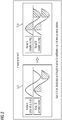
- Figure 2 shows an exemplary phase shift for the phase control.
- a curve of a mains voltage or alternating supply voltage is shown as a sine wave.
- the load is activated in each network half-cycle after a certain delay time from the previous current zero crossing.
- Each dimming channel (channel A, channel B) has a device with which it is able to monitor the temperature of its switching elements. If the temperature at the switching element rises, it can be assumed that the channel switches on too early. In the left scenario SZ1 according to the exemplary illustration Figure 2 switches channel A too early. This is recognized by the control unit of channel A (eg through appropriate temperature monitoring).
- the control unit of dimming channel A causes the dimming edge of channel A to move backwards in time (ie in the illustration according to FIG Figure 2 to the right) (see scenario SZ2 according to the exemplary illustration Figure 2 ).
- scenario SZ2 according to the example illustration Figure 2 switch channel A and channel B synchronously again.
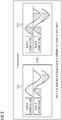
- Figure 3 shows an exemplary phase shift for the phase section.
- a curve of a mains voltage or alternating supply voltage is shown as a sine wave. With trailing edge operation, the load is in each half-wave
- Each dimming channel (channel A, channel B) has a device with which it is able to monitor the temperature of its switching elements. If the temperature at the switching element increases, it can be assumed that the channel switches on too late.
- the left scenario SZ3 according to the exemplary illustration Figure 3 switches channel A too late. This is recognized by the control unit of channel A (eg through appropriate temperature monitoring).
- the control unit of dimming channel A causes the dimming edge of channel A to move forward in time (ie in the illustration according to FIG Figure 3 to the left) (see scenario SZ4 according to the example illustration Figure 3 ).
- scenario SZ4 according to the example illustration Figure 3 switch channel A and channel B synchronously again.
- FIG 4 shows an exemplary flowchart for carrying out the method according to the invention for controlling the power consumption of a load that can be connected to a dimmer system, in particular an LED light, the dimmer system (DS) comprising at least two galvanically isolated dimming channels connected in parallel, (VS1) being based on the temperature of the Switching elements of the respective dimming channel, the dimming edge of the respective dimming channel is shifted in order to distribute the power loss of the connected load essentially evenly over the dimming channels.
- DS dimmer system
- VS1 galvanically isolated dimming channels connected in parallel
- the respective dimming edge of the respective dimming channel is advantageously shifted forwards or backwards in time.
- the respective dimming edge is advantageously shifted forward or backward in time until the gradient of the temperature of the respective switching elements decreases.
- the respective dimming edge is advantageously shifted forward or backward in time until the temperature of the respective switching elements stagnates.
- the respective dimming edge is shifted forwards or backwards in time until the temperature of the respective switching elements is reduced.
- the process can be implemented with commercially available components (e.g. semiconductor temperature sensors) or with components (e.g. transistors, switching elements) that a dimmer system has anyway.
- components e.g. semiconductor temperature sensors
- components e.g. transistors, switching elements
Landscapes
- Physics & Mathematics (AREA)
- Engineering & Computer Science (AREA)
- Microelectronics & Electronic Packaging (AREA)
- Optics & Photonics (AREA)
- Circuit Arrangement For Electric Light Sources In General (AREA)
Claims (8)
- Système gradateur de lumière (DS) pour commander la puissance absorbée d'une charge raccordable (L), et plus particulièrement d'une lampe LED, le système gradateur de lumière comportant au moins deux canaux de gradation montés en parallèles et séparés galvaniquement(DK_A, DK_B, DK_X), chaque canal de gradation (DK_A, DK_B, DK_X) comprenant un dispositif (TS1 - TS3) pour surveiller la température de ses éléments de commutation, caractérisé en ce que chaque canal de gradation (DK_A, DK_B, DK_X) comprend une unité de commande (SE1 - SE3) pour décaler son flanc de gradation sur la base de la température (T) de ses éléments de commutation pour répartir la dissipation de puissance de la charge raccordée (L) de manière sensiblement uniforme sur les canaux de gradation (DK_A, DK_B, DK_X), le flanc de gradation respective du canal de gradation respectif (DK_A, DK_B, DK_X) étant, pour synchroniser les canaux de gradation, décalée temporellement vers l'avant ou vers l'arrière par l'unité de commande du canal de gradation respectif (DK_A, DK_B, DK_X) en fonction de la température des éléments de commutation respectifs.
- Système gradateur de lumière (DS) selon la revendication 1, le décalage temporel du flanc de gradation respective vers l'avant ou vers l'arrière se faisant jusqu'à ce que le gradient de la température des éléments de commutation respectifs se réduise.
- Système gradateur de lumière (DS) selon l'une des revendications précédentes, le décalage temporel du flanc de gradation respective vers l'avant ou vers l'arrière se faisant jusqu'à ce que la température des éléments de commutation respectifs stagne.
- Système gradateur de lumière (DS) selon l'une des revendications précédentes, le décalage temporel du flanc de gradation respective vers l'avant ou vers l'arrière se faisant jusqu'à ce que la température des éléments de commutation respectifs se réduise.
- Système gradateur de lumière (DS) selon l'une des revendications précédentes, comprenant en outre une unité de commande maître (MSE) qui est reliée, en termes de données, avec les unités de commande des canaux de gradation (DK_A, DK_B, DK_X), l'unité de commande maître (MSE) spécifiant une valeur de consigne aux unités de commande des canaux de gradation (DK_A, DK_B, DK_X), le décalage respectif des flancs de gradation se basant sur la valeur de consigne.
- Système gradateur de lumière (DS) selon la revendication 5, la valeur de consigne se basant sur la température des éléments de commutation montés dans le système gradateur de lumière.
- Système gradateur de lumière (DS) selon l'une des revendications précédentes, les canaux de gradation (DK_A, DK_B, DK_X) étant agencés sur un moyen de refroidissement (KM) commun, et plus particulièrement sur une tôle de refroidissement.
- Procédé de commande de la puissance absorbée d'une charge (L) pouvant être raccordée à un système gradateur de lumière (DS), et plus particulièrement d'une lampe LED, le système gradateur de lumière (DS) comportant au moins deux canaux de gradation montés en parallèles et séparés galvaniquement(DK _A, DK_B, DK_X), chaque canal de gradation (DK_A, DK_B, DK_X) comprenant un dispositif (TS1 - TS3) pour surveiller la température de ses éléments de commutation, caractérisé en ce que chaque canal de gradation (DK_A, DK_B, DK_X) comprend une unité de commande (SE1 - SE3) pour décaler son flanc de gradation,
sur la base de la température des éléments de commutation du canal de gradation respectif (DK_A, DK_B, DK_X) se produisant un décalage du flanc de gradation du canal de gradation respectif (DK_A, DK_B, DK_X) pour répartir la dissipation de puissance de la charge raccordée (L) de manière sensiblement uniforme sur les canaux de gradation (DK_A, DK_B, DK_X),
le flanc de gradation respective du canal de gradation respectif (DK_A, DK_B, DK_X) étant, pour synchroniser les canaux de gradation, décalée temporellement vers l'avant ou vers l'arrière par l'unité de commande du canal de gradation respectif (DK_A, DK_B, DK_X) en fonction de la température des éléments de commutation respectifs.
Applications Claiming Priority (2)
| Application Number | Priority Date | Filing Date | Title |
|---|---|---|---|
| DE102017215643.0A DE102017215643B3 (de) | 2017-09-06 | 2017-09-06 | Dimmersystem und Verfahren zur Steuerung der Leistungsaufnahme einer an ein Dimmersystem anschliessbaren Last |
| PCT/EP2018/071632 WO2019048175A1 (fr) | 2017-09-06 | 2018-08-09 | Système variateur |
Publications (2)
| Publication Number | Publication Date |
|---|---|
| EP3679768A1 EP3679768A1 (fr) | 2020-07-15 |
| EP3679768B1 true EP3679768B1 (fr) | 2021-04-21 |
Family
ID=62813185
Family Applications (1)
| Application Number | Title | Priority Date | Filing Date |
|---|---|---|---|
| EP18759865.1A Active EP3679768B1 (fr) | 2017-09-06 | 2018-08-09 | Système gradateur de lumière |
Country Status (6)
| Country | Link |
|---|---|
| US (1) | US11032883B2 (fr) |
| EP (1) | EP3679768B1 (fr) |
| CN (1) | CN111096075B (fr) |
| DE (1) | DE102017215643B3 (fr) |
| ES (1) | ES2881186T3 (fr) |
| WO (1) | WO2019048175A1 (fr) |
Families Citing this family (2)
| Publication number | Priority date | Publication date | Assignee | Title |
|---|---|---|---|---|
| DE102017215643B3 (de) | 2017-09-06 | 2018-07-26 | Siemens Schweiz Ag | Dimmersystem und Verfahren zur Steuerung der Leistungsaufnahme einer an ein Dimmersystem anschliessbaren Last |
| DE102018009924B4 (de) | 2018-12-17 | 2020-10-01 | Siemens Schweiz Ag | Dimmer und Verfahren zum Erkennen der korrekten Verdrahtung von Dimmkanälen |
Family Cites Families (11)
| Publication number | Priority date | Publication date | Assignee | Title |
|---|---|---|---|---|
| US7471051B1 (en) * | 2004-09-24 | 2008-12-30 | Avatar Systems Llc | Advanced low voltage lighting system |
| DE102006036293A1 (de) | 2006-08-03 | 2008-02-14 | Cooper Crouse-Hinds Gmbh | Überwachungsvorrichtung |
| US20090267523A1 (en) * | 2008-04-24 | 2009-10-29 | Articulated Technologies, Llc | Driver circuit for light sheet module with direct connection to power source |
| DE102008030365A1 (de) | 2008-06-26 | 2009-08-20 | Continental Automotive Gmbh | Einrichtung zur Ansteuerung von in einem Array angeordneten Einzellichtquellen |
| US8957601B2 (en) * | 2008-09-18 | 2015-02-17 | Lumastream Canada Ulc | Configurable LED driver/dimmer for solid state lighting applications |
| US20130328505A1 (en) | 2012-06-08 | 2013-12-12 | Laurence P. Sadwick | Dimmer for Dimmable Drivers |
| KR101568752B1 (ko) | 2013-07-18 | 2015-11-12 | 주식회사 루멘스 | 복수의 엘이디동작부를 포함하는 엘이디 조명장치 |
| EP2925095B1 (fr) | 2014-03-28 | 2020-09-23 | Helvar Oy Ab | Contrôleur d'éclairage |
| CN204836682U (zh) | 2015-07-21 | 2015-12-02 | 武汉全华光电科技股份有限公司 | 一种智能型亮度调节照明组件控制线路 |
| DE102016209278B3 (de) | 2016-05-30 | 2017-08-10 | Siemens Schweiz Ag | Dimmersystem |
| DE102017215643B3 (de) | 2017-09-06 | 2018-07-26 | Siemens Schweiz Ag | Dimmersystem und Verfahren zur Steuerung der Leistungsaufnahme einer an ein Dimmersystem anschliessbaren Last |
-
2017
- 2017-09-06 DE DE102017215643.0A patent/DE102017215643B3/de not_active Expired - Fee Related
-
2018
- 2018-08-09 ES ES18759865T patent/ES2881186T3/es active Active
- 2018-08-09 EP EP18759865.1A patent/EP3679768B1/fr active Active
- 2018-08-09 US US16/643,945 patent/US11032883B2/en active Active
- 2018-08-09 WO PCT/EP2018/071632 patent/WO2019048175A1/fr not_active Ceased
- 2018-08-09 CN CN201880057930.7A patent/CN111096075B/zh active Active
Also Published As
| Publication number | Publication date |
|---|---|
| CN111096075A (zh) | 2020-05-01 |
| CN111096075B (zh) | 2022-04-19 |
| EP3679768A1 (fr) | 2020-07-15 |
| US11032883B2 (en) | 2021-06-08 |
| DE102017215643B3 (de) | 2018-07-26 |
| WO2019048175A1 (fr) | 2019-03-14 |
| ES2881186T3 (es) | 2021-11-29 |
| US20200413504A1 (en) | 2020-12-31 |
Similar Documents
| Publication | Publication Date | Title |
|---|---|---|
| EP0618667B1 (fr) | Procédé pour commander une charge en courant alternatif et dispositif pour mettre en oeuvre ce procédé | |
| EP0901313B1 (fr) | Système gradateur | |
| EP3253182B1 (fr) | Système gradateur de lumière | |
| DE10315554B3 (de) | Dimmer Booster | |
| EP3679768B1 (fr) | Système gradateur de lumière | |
| AT413916B (de) | Verfahren und vorrichtung zur erkennung und steuerung von elektronischen schaltnetzteilen oder konventionellen transformatoren, jeweils mit oder ohne ohmscher last, insbesondere von beleuchtungseinrichtungen | |
| DE102010052662B4 (de) | Datentelegramm-Generierungsverfahren zur Ansteuerung mindestens eines Lastmoduls bzw. einer Lampe über eine Lastleitung | |
| EP3125647B1 (fr) | Attenuation de dispositifs d'eclairage | |
| EP3672375B1 (fr) | Variateur de luminosité | |
| DE102009034801A1 (de) | Verfahren zur Ansteuerung einer Leuchte | |
| DE102010000533B4 (de) | Steuergerät zum Übertragen einer Steuerinformation an eine Lampeneinheit sowie Verfahren zum Betreiben eines solchen Steuergerätes | |
| DE102006033765B3 (de) | Dimmersystem mit mehreren Multidimmern und Multidimmer, welcher universell als Masterdimmer, als Slavedimmer oder als Nebenstelle einsetzbar ist | |
| DE102016210448B4 (de) | LED-Leuchte mit LED-Leuchtmitteln unterschiedlicher Farbtemperatur | |
| WO2016058592A1 (fr) | Circuit permettant de faire fonctionner des diodes électroluminescentes de manière conforme à un réseau et moyen d'éclairage et luminaire | |
| DE102019131275A1 (de) | Phasendimmer sowie Verfahren zum Betreiben desselben | |
| EP1952521B1 (fr) | Variateur universel double | |
| DE102006062751A1 (de) | Multidimmer, welcher universell als Masterdimmer, als Slavedimmer oder als Nebenstelle einsetzbar ist | |
| DE10310591B4 (de) | Elektronisches Vorschaltgerät und Schaltungsanordnung zum Betreiben einer Gasentladungslampe | |
| DE102012112641B4 (de) | Vorrichtung und Verfahren zur Erkennung einer durch eine elektronische Steuerschaltung ansteuerbaren Lastart in einer Beleuchtungsinstallation | |
| EP1370119B1 (fr) | Gradateur à canaux multiples | |
| WO2005074321A2 (fr) | Procede pour commander des dispositifs de chauffe dans un appareil de cuisson electrique, et dispositif correspondant | |
| DE102006016392A1 (de) | Elektronikschaltung zum Schalten/Dimmen von Wechselströmen unter Einsatz eines Triacs | |
| EP1615314B1 (fr) | Circuit pour la reconnaissance des demi-ondes d'une tension 230V courant alternatif | |
| DE102020108475A1 (de) | Leistungssteuerungsschaltung, leistungssteuerungsverfahren | |
| DE102016102348A1 (de) | Transformatorloses Netzteil, insbesondere für LED-Beleuchtungssysteme |
Legal Events
| Date | Code | Title | Description |
|---|---|---|---|
| STAA | Information on the status of an ep patent application or granted ep patent |
Free format text: STATUS: UNKNOWN |
|
| STAA | Information on the status of an ep patent application or granted ep patent |
Free format text: STATUS: THE INTERNATIONAL PUBLICATION HAS BEEN MADE |
|
| PUAI | Public reference made under article 153(3) epc to a published international application that has entered the european phase |
Free format text: ORIGINAL CODE: 0009012 |
|
| STAA | Information on the status of an ep patent application or granted ep patent |
Free format text: STATUS: REQUEST FOR EXAMINATION WAS MADE |
|
| 17P | Request for examination filed |
Effective date: 20200205 |
|
| AK | Designated contracting states |
Kind code of ref document: A1 Designated state(s): AL AT BE BG CH CY CZ DE DK EE ES FI FR GB GR HR HU IE IS IT LI LT LU LV MC MK MT NL NO PL PT RO RS SE SI SK SM TR |
|
| AX | Request for extension of the european patent |
Extension state: BA ME |
|
| REG | Reference to a national code |
Ref country code: DE Ref legal event code: R079 Ref document number: 502018004944 Country of ref document: DE Free format text: PREVIOUS MAIN CLASS: H05B0033080000 Ipc: H05B0045500000 |
|
| DAV | Request for validation of the european patent (deleted) | ||
| DAX | Request for extension of the european patent (deleted) | ||
| GRAP | Despatch of communication of intention to grant a patent |
Free format text: ORIGINAL CODE: EPIDOSNIGR1 |
|
| STAA | Information on the status of an ep patent application or granted ep patent |
Free format text: STATUS: GRANT OF PATENT IS INTENDED |
|
| RIC1 | Information provided on ipc code assigned before grant |
Ipc: H05B 39/04 20060101ALI20201210BHEP Ipc: H05B 45/50 20200101AFI20201210BHEP |
|
| INTG | Intention to grant announced |
Effective date: 20210104 |
|
| INTG | Intention to grant announced |
Effective date: 20210113 |
|
| GRAS | Grant fee paid |
Free format text: ORIGINAL CODE: EPIDOSNIGR3 |
|
| GRAA | (expected) grant |
Free format text: ORIGINAL CODE: 0009210 |
|
| STAA | Information on the status of an ep patent application or granted ep patent |
Free format text: STATUS: THE PATENT HAS BEEN GRANTED |
|
| AK | Designated contracting states |
Kind code of ref document: B1 Designated state(s): AL AT BE BG CH CY CZ DE DK EE ES FI FR GB GR HR HU IE IS IT LI LT LU LV MC MK MT NL NO PL PT RO RS SE SI SK SM TR |
|
| REG | Reference to a national code |
Ref country code: GB Ref legal event code: FG4D Free format text: NOT ENGLISH |
|
| REG | Reference to a national code |
Ref country code: CH Ref legal event code: EP |
|
| REG | Reference to a national code |
Ref country code: DE Ref legal event code: R096 Ref document number: 502018004944 Country of ref document: DE |
|
| REG | Reference to a national code |
Ref country code: IE Ref legal event code: FG4D Free format text: LANGUAGE OF EP DOCUMENT: GERMAN |
|
| REG | Reference to a national code |
Ref country code: AT Ref legal event code: REF Ref document number: 1386008 Country of ref document: AT Kind code of ref document: T Effective date: 20210515 |
|
| REG | Reference to a national code |
Ref country code: NL Ref legal event code: FP |
|
| REG | Reference to a national code |
Ref country code: SE Ref legal event code: TRGR |
|
| REG | Reference to a national code |
Ref country code: LT Ref legal event code: MG9D |
|
| PG25 | Lapsed in a contracting state [announced via postgrant information from national office to epo] |
Ref country code: LT Free format text: LAPSE BECAUSE OF FAILURE TO SUBMIT A TRANSLATION OF THE DESCRIPTION OR TO PAY THE FEE WITHIN THE PRESCRIBED TIME-LIMIT Effective date: 20210421 Ref country code: HR Free format text: LAPSE BECAUSE OF FAILURE TO SUBMIT A TRANSLATION OF THE DESCRIPTION OR TO PAY THE FEE WITHIN THE PRESCRIBED TIME-LIMIT Effective date: 20210421 Ref country code: FI Free format text: LAPSE BECAUSE OF FAILURE TO SUBMIT A TRANSLATION OF THE DESCRIPTION OR TO PAY THE FEE WITHIN THE PRESCRIBED TIME-LIMIT Effective date: 20210421 Ref country code: BG Free format text: LAPSE BECAUSE OF FAILURE TO SUBMIT A TRANSLATION OF THE DESCRIPTION OR TO PAY THE FEE WITHIN THE PRESCRIBED TIME-LIMIT Effective date: 20210721 |
|
| REG | Reference to a national code |
Ref country code: ES Ref legal event code: FG2A Ref document number: 2881186 Country of ref document: ES Kind code of ref document: T3 Effective date: 20211129 |
|
| PG25 | Lapsed in a contracting state [announced via postgrant information from national office to epo] |
Ref country code: PT Free format text: LAPSE BECAUSE OF FAILURE TO SUBMIT A TRANSLATION OF THE DESCRIPTION OR TO PAY THE FEE WITHIN THE PRESCRIBED TIME-LIMIT Effective date: 20210823 Ref country code: RS Free format text: LAPSE BECAUSE OF FAILURE TO SUBMIT A TRANSLATION OF THE DESCRIPTION OR TO PAY THE FEE WITHIN THE PRESCRIBED TIME-LIMIT Effective date: 20210421 Ref country code: NO Free format text: LAPSE BECAUSE OF FAILURE TO SUBMIT A TRANSLATION OF THE DESCRIPTION OR TO PAY THE FEE WITHIN THE PRESCRIBED TIME-LIMIT Effective date: 20210721 Ref country code: LV Free format text: LAPSE BECAUSE OF FAILURE TO SUBMIT A TRANSLATION OF THE DESCRIPTION OR TO PAY THE FEE WITHIN THE PRESCRIBED TIME-LIMIT Effective date: 20210421 Ref country code: PL Free format text: LAPSE BECAUSE OF FAILURE TO SUBMIT A TRANSLATION OF THE DESCRIPTION OR TO PAY THE FEE WITHIN THE PRESCRIBED TIME-LIMIT Effective date: 20210421 Ref country code: GR Free format text: LAPSE BECAUSE OF FAILURE TO SUBMIT A TRANSLATION OF THE DESCRIPTION OR TO PAY THE FEE WITHIN THE PRESCRIBED TIME-LIMIT Effective date: 20210722 Ref country code: IS Free format text: LAPSE BECAUSE OF FAILURE TO SUBMIT A TRANSLATION OF THE DESCRIPTION OR TO PAY THE FEE WITHIN THE PRESCRIBED TIME-LIMIT Effective date: 20210821 |
|
| REG | Reference to a national code |
Ref country code: DE Ref legal event code: R097 Ref document number: 502018004944 Country of ref document: DE |
|
| PG25 | Lapsed in a contracting state [announced via postgrant information from national office to epo] |
Ref country code: EE Free format text: LAPSE BECAUSE OF FAILURE TO SUBMIT A TRANSLATION OF THE DESCRIPTION OR TO PAY THE FEE WITHIN THE PRESCRIBED TIME-LIMIT Effective date: 20210421 Ref country code: SK Free format text: LAPSE BECAUSE OF FAILURE TO SUBMIT A TRANSLATION OF THE DESCRIPTION OR TO PAY THE FEE WITHIN THE PRESCRIBED TIME-LIMIT Effective date: 20210421 Ref country code: DK Free format text: LAPSE BECAUSE OF FAILURE TO SUBMIT A TRANSLATION OF THE DESCRIPTION OR TO PAY THE FEE WITHIN THE PRESCRIBED TIME-LIMIT Effective date: 20210421 Ref country code: CZ Free format text: LAPSE BECAUSE OF FAILURE TO SUBMIT A TRANSLATION OF THE DESCRIPTION OR TO PAY THE FEE WITHIN THE PRESCRIBED TIME-LIMIT Effective date: 20210421 Ref country code: RO Free format text: LAPSE BECAUSE OF FAILURE TO SUBMIT A TRANSLATION OF THE DESCRIPTION OR TO PAY THE FEE WITHIN THE PRESCRIBED TIME-LIMIT Effective date: 20210421 Ref country code: SM Free format text: LAPSE BECAUSE OF FAILURE TO SUBMIT A TRANSLATION OF THE DESCRIPTION OR TO PAY THE FEE WITHIN THE PRESCRIBED TIME-LIMIT Effective date: 20210421 |
|
| PLBE | No opposition filed within time limit |
Free format text: ORIGINAL CODE: 0009261 |
|
| STAA | Information on the status of an ep patent application or granted ep patent |
Free format text: STATUS: NO OPPOSITION FILED WITHIN TIME LIMIT |
|
| 26N | No opposition filed |
Effective date: 20220124 |
|
| PG25 | Lapsed in a contracting state [announced via postgrant information from national office to epo] |
Ref country code: MC Free format text: LAPSE BECAUSE OF FAILURE TO SUBMIT A TRANSLATION OF THE DESCRIPTION OR TO PAY THE FEE WITHIN THE PRESCRIBED TIME-LIMIT Effective date: 20210421 |
|
| REG | Reference to a national code |
Ref country code: BE Ref legal event code: MM Effective date: 20210831 |
|
| PG25 | Lapsed in a contracting state [announced via postgrant information from national office to epo] |
Ref country code: IS Free format text: LAPSE BECAUSE OF FAILURE TO SUBMIT A TRANSLATION OF THE DESCRIPTION OR TO PAY THE FEE WITHIN THE PRESCRIBED TIME-LIMIT Effective date: 20210821 Ref country code: LU Free format text: LAPSE BECAUSE OF NON-PAYMENT OF DUE FEES Effective date: 20210809 Ref country code: AL Free format text: LAPSE BECAUSE OF FAILURE TO SUBMIT A TRANSLATION OF THE DESCRIPTION OR TO PAY THE FEE WITHIN THE PRESCRIBED TIME-LIMIT Effective date: 20210421 |
|
| PG25 | Lapsed in a contracting state [announced via postgrant information from national office to epo] |
Ref country code: IE Free format text: LAPSE BECAUSE OF NON-PAYMENT OF DUE FEES Effective date: 20210809 Ref country code: BE Free format text: LAPSE BECAUSE OF NON-PAYMENT OF DUE FEES Effective date: 20210831 |
|
| P01 | Opt-out of the competence of the unified patent court (upc) registered |
Effective date: 20230523 |
|
| PG25 | Lapsed in a contracting state [announced via postgrant information from national office to epo] |
Ref country code: CY Free format text: LAPSE BECAUSE OF FAILURE TO SUBMIT A TRANSLATION OF THE DESCRIPTION OR TO PAY THE FEE WITHIN THE PRESCRIBED TIME-LIMIT Effective date: 20210421 |
|
| PG25 | Lapsed in a contracting state [announced via postgrant information from national office to epo] |
Ref country code: HU Free format text: LAPSE BECAUSE OF FAILURE TO SUBMIT A TRANSLATION OF THE DESCRIPTION OR TO PAY THE FEE WITHIN THE PRESCRIBED TIME-LIMIT; INVALID AB INITIO Effective date: 20180809 |
|
| PG25 | Lapsed in a contracting state [announced via postgrant information from national office to epo] |
Ref country code: MK Free format text: LAPSE BECAUSE OF FAILURE TO SUBMIT A TRANSLATION OF THE DESCRIPTION OR TO PAY THE FEE WITHIN THE PRESCRIBED TIME-LIMIT Effective date: 20210421 |
|
| PG25 | Lapsed in a contracting state [announced via postgrant information from national office to epo] |
Ref country code: MT Free format text: LAPSE BECAUSE OF FAILURE TO SUBMIT A TRANSLATION OF THE DESCRIPTION OR TO PAY THE FEE WITHIN THE PRESCRIBED TIME-LIMIT Effective date: 20210421 |
|
| PGFP | Annual fee paid to national office [announced via postgrant information from national office to epo] |
Ref country code: NL Payment date: 20250811 Year of fee payment: 8 |
|
| PGFP | Annual fee paid to national office [announced via postgrant information from national office to epo] |
Ref country code: TR Payment date: 20250804 Year of fee payment: 8 Ref country code: IT Payment date: 20250827 Year of fee payment: 8 |
|
| PGFP | Annual fee paid to national office [announced via postgrant information from national office to epo] |
Ref country code: GB Payment date: 20250902 Year of fee payment: 8 |
|
| PGFP | Annual fee paid to national office [announced via postgrant information from national office to epo] |
Ref country code: AT Payment date: 20250708 Year of fee payment: 8 Ref country code: FR Payment date: 20250827 Year of fee payment: 8 |
|
| PGFP | Annual fee paid to national office [announced via postgrant information from national office to epo] |
Ref country code: SE Payment date: 20250819 Year of fee payment: 8 |
|
| REG | Reference to a national code |
Ref country code: CH Ref legal event code: U11 Free format text: ST27 STATUS EVENT CODE: U-0-0-U10-U11 (AS PROVIDED BY THE NATIONAL OFFICE) Effective date: 20251110 |
|
| PGFP | Annual fee paid to national office [announced via postgrant information from national office to epo] |
Ref country code: DE Payment date: 20251020 Year of fee payment: 8 |
|
| PGFP | Annual fee paid to national office [announced via postgrant information from national office to epo] |
Ref country code: CH Payment date: 20251110 Year of fee payment: 8 |
|
| PGFP | Annual fee paid to national office [announced via postgrant information from national office to epo] |
Ref country code: ES Payment date: 20251124 Year of fee payment: 8 |