EP3680122B1 - Kurzschlussfestigkeit eines begleiterchips - Google Patents
Kurzschlussfestigkeit eines begleiterchips Download PDFInfo
- Publication number
- EP3680122B1 EP3680122B1 EP19305029.1A EP19305029A EP3680122B1 EP 3680122 B1 EP3680122 B1 EP 3680122B1 EP 19305029 A EP19305029 A EP 19305029A EP 3680122 B1 EP3680122 B1 EP 3680122B1
- Authority
- EP
- European Patent Office
- Prior art keywords
- current
- predetermined value
- circuit
- magnitude
- wheel speed
- Prior art date
- Legal status (The legal status is an assumption and is not a legal conclusion. Google has not performed a legal analysis and makes no representation as to the accuracy of the status listed.)
- Active
Links
Images



Classifications
-
- B—PERFORMING OPERATIONS; TRANSPORTING
- B60—VEHICLES IN GENERAL
- B60L—PROPULSION OF ELECTRICALLY-PROPELLED VEHICLES; SUPPLYING ELECTRIC POWER FOR AUXILIARY EQUIPMENT OF ELECTRICALLY-PROPELLED VEHICLES; ELECTRODYNAMIC BRAKE SYSTEMS FOR VEHICLES IN GENERAL; MAGNETIC SUSPENSION OR LEVITATION FOR VEHICLES; MONITORING OPERATING VARIABLES OF ELECTRICALLY-PROPELLED VEHICLES; ELECTRIC SAFETY DEVICES FOR ELECTRICALLY-PROPELLED VEHICLES
- B60L3/00—Electric devices on electrically-propelled vehicles for safety purposes; Monitoring operating variables, e.g. speed, deceleration or energy consumption
- B60L3/0023—Detecting, eliminating, remedying or compensating for drive train abnormalities, e.g. failures within the drive train
- B60L3/0038—Detecting, eliminating, remedying or compensating for drive train abnormalities, e.g. failures within the drive train relating to sensors
-
- G—PHYSICS
- G01—MEASURING; TESTING
- G01P—MEASURING LINEAR OR ANGULAR SPEED, ACCELERATION, DECELERATION, OR SHOCK; INDICATING PRESENCE, ABSENCE, OR DIRECTION, OF MOVEMENT
- G01P3/00—Measuring linear or angular speed; Measuring differences of linear or angular speeds
- G01P3/42—Devices characterised by the use of electric or magnetic means
- G01P3/44—Devices characterised by the use of electric or magnetic means for measuring angular speed
- G01P3/48—Devices characterised by the use of electric or magnetic means for measuring angular speed by measuring frequency of generated current or voltage
- G01P3/4802—Devices characterised by the use of electric or magnetic means for measuring angular speed by measuring frequency of generated current or voltage by using electronic circuits in general
-
- B—PERFORMING OPERATIONS; TRANSPORTING
- B60—VEHICLES IN GENERAL
- B60L—PROPULSION OF ELECTRICALLY-PROPELLED VEHICLES; SUPPLYING ELECTRIC POWER FOR AUXILIARY EQUIPMENT OF ELECTRICALLY-PROPELLED VEHICLES; ELECTRODYNAMIC BRAKE SYSTEMS FOR VEHICLES IN GENERAL; MAGNETIC SUSPENSION OR LEVITATION FOR VEHICLES; MONITORING OPERATING VARIABLES OF ELECTRICALLY-PROPELLED VEHICLES; ELECTRIC SAFETY DEVICES FOR ELECTRICALLY-PROPELLED VEHICLES
- B60L3/00—Electric devices on electrically-propelled vehicles for safety purposes; Monitoring operating variables, e.g. speed, deceleration or energy consumption
- B60L3/10—Indicating wheel slip ; Correction of wheel slip
- B60L3/102—Indicating wheel slip ; Correction of wheel slip of individual wheels
-
- B—PERFORMING OPERATIONS; TRANSPORTING
- B60—VEHICLES IN GENERAL
- B60L—PROPULSION OF ELECTRICALLY-PROPELLED VEHICLES; SUPPLYING ELECTRIC POWER FOR AUXILIARY EQUIPMENT OF ELECTRICALLY-PROPELLED VEHICLES; ELECTRODYNAMIC BRAKE SYSTEMS FOR VEHICLES IN GENERAL; MAGNETIC SUSPENSION OR LEVITATION FOR VEHICLES; MONITORING OPERATING VARIABLES OF ELECTRICALLY-PROPELLED VEHICLES; ELECTRIC SAFETY DEVICES FOR ELECTRICALLY-PROPELLED VEHICLES
- B60L3/00—Electric devices on electrically-propelled vehicles for safety purposes; Monitoring operating variables, e.g. speed, deceleration or energy consumption
- B60L3/10—Indicating wheel slip ; Correction of wheel slip
- B60L3/104—Indicating wheel slip ; Correction of wheel slip by indirect measurement of vehicle speed
-
- G—PHYSICS
- G01—MEASURING; TESTING
- G01P—MEASURING LINEAR OR ANGULAR SPEED, ACCELERATION, DECELERATION, OR SHOCK; INDICATING PRESENCE, ABSENCE, OR DIRECTION, OF MOVEMENT
- G01P3/00—Measuring linear or angular speed; Measuring differences of linear or angular speeds
- G01P3/42—Devices characterised by the use of electric or magnetic means
- G01P3/44—Devices characterised by the use of electric or magnetic means for measuring angular speed
- G01P3/48—Devices characterised by the use of electric or magnetic means for measuring angular speed by measuring frequency of generated current or voltage
- G01P3/481—Devices characterised by the use of electric or magnetic means for measuring angular speed by measuring frequency of generated current or voltage of pulse signals
- G01P3/489—Digital circuits therefor
-
- B—PERFORMING OPERATIONS; TRANSPORTING
- B60—VEHICLES IN GENERAL
- B60L—PROPULSION OF ELECTRICALLY-PROPELLED VEHICLES; SUPPLYING ELECTRIC POWER FOR AUXILIARY EQUIPMENT OF ELECTRICALLY-PROPELLED VEHICLES; ELECTRODYNAMIC BRAKE SYSTEMS FOR VEHICLES IN GENERAL; MAGNETIC SUSPENSION OR LEVITATION FOR VEHICLES; MONITORING OPERATING VARIABLES OF ELECTRICALLY-PROPELLED VEHICLES; ELECTRIC SAFETY DEVICES FOR ELECTRICALLY-PROPELLED VEHICLES
- B60L2240/00—Control parameters of input or output; Target parameters
- B60L2240/40—Drive Train control parameters
- B60L2240/46—Drive Train control parameters related to wheels
- B60L2240/461—Speed
Definitions
- Sensors detect events or quantities, and provide output signals indicative thereof.
- wheel speed sensors output signals indicative of wheel speed. These output signals can be used by control systems such as an anti-lock brake system (ABS).
- ABS anti-lock brake system
- Active wheel speed sensors are commonly used in newer vehicles for various reasons. Some active wheel speed sensors (hereinafter type I active wheel speed sensors) output a square wave current signal, the frequency of which is determined by the rotational speed of an associated wheel. The magnitude of signals produced by other types of active wheel speed sensors may vary depending on whether its associated wheel is rotating in a forward or reverse direction. Yet other types of active wheel speed sensors output pulse-width modulated signals in which additional information such as direction of rotation and magnetic field strength are coded. The output of still other types of active wheel speed sensors are encoded with diagnostic data. The present technology will be described with reference to type I active wheel speed sensors employed in motorized vehicles, it being understood the present technology should not be limited thereto.
- U.S. Patent Application No. 16/055,554 describes an example ABS that employs wheel speed sensors.
- the application describes interface circuits connected between wheel speed sensors (WSS) and an ABS controller.
- WSS wheel speed sensors
- Each interface circuit decodes a square wave output signal of a WSS to produce rotational information for subsequent processing by the ABS controller.
- the ABS controller performs several functions such as monitoring rotational speed of all wheels of the vehicle. If the speed from one wheel changes abruptly with respect to the speed of other wheels, the ABS controller understands that wheel is beginning to lose traction. It can take appropriate action such as applying the brakes or performing traction control.
- US patent application publication number US 2017/02909625 discloses a wheel sensor interface apparatus which includes an interface unit configured to supply power to a wheel sensor of a vehicle or sense an output current of the wheel sensor and transmit the sensor current to a microprocessor unit of the vehicle, and an overcurrent detection unit including a reference current generation unit configured to generate a reference current using a voltage across the resistor through which the output current flows.
- US2003226702 discloses a system comprising a torque distribution device for distributing driving power from an engine to the wheels. In the control device, abnormality judgement means judges whether or not an abnormality is involved in wheel speed signals which are input from wheel speed sensors associated respectively with the front and rear wheels.
- US2010182725 discloses a circuit arrangement connected to at least one wheel speed sensor channel for transmitting wheel speed information, said arrangement comprising a blocking circuit for blocking a wheel speed sensor if an overcurrent abnormality is detected.
- Figure 1 illustrates relevant components of an example ABS 100 that includes a WSS 102 that is closely positioned to a gear-shaped rotor (also known as a tone wheel) 104, which in turn is attached directly or indirectly to a wheel of a motor vehicle (not shown).
- Figure 1 also shows a WSS interface circuit 110 coupled to WSS 102 and controlled by ABS controller 114.
- ABS controller 114 may take form in a microcontroller or system-on-a-chip that includes one or more central processing units, each of which is capable of executing instructions stored in memory. ABS controller 114 performs various functions in response to executing the instructions.
- Equally spaced teeth are positioned on the circumference of rotor 104, which spins at a speed that matches the rotational speed of the wheel to which it is attached.
- WSS 102 draws current IH from a voltage supply Vss provided by a battery (not shown) via interface circuit 110.
- WSS 102 returns current IL to ground via interface circuit 110.
- Normally IL IH.
- FIG. 1 shows a square wave that represents IL as rotor 104 spins.
- Each pulse of IL shown in Figure 1 represents a tooth passing WSS 102.
- IL varies between 14 mA and 7 mA.
- the frequency of pulses is directly proportional to wheel speed since rotor 104, which is directly or indirectly attached to the wheel. As the rotation speed of rotor 104 increases, the frequency of pulses increases, thereby indicating faster wheel speed.
- the frequency of pulses can be used to determine wheel speed.
- Interface circuit 110 decodes IL or IH to produce an output voltage signal WS1 that can be understood by ABS controller 114. Normally interface circuit 110 decodes IL. However, interface circuit 110 will decode IH if interface circuit 110 determines that IL is greater in magnitude than IH.
- U.S. Patent Application No. 16/055,554 describes at least one situation in which IL will be greater in magnitude.
- a threshold value X e.g. 10 mA
- Interface circuit 110 decodes IL to produce WS1 shown in Figure 1 .
- WS1 is a square wave that normally switches between 5V and 0V as IL switches between 7 mA and 14 mA.
- the frequency of WS1 matches the frequency of IL, which in turn depends on the rotational speed of rotor 104.
- WS1 is provided to ABS controller 114 as wheel speed information.
- ABS controller 114 generates traction control signals C1 - C4 in response to processing wheel speed signals WS1 - WS4, respectively, received from respective interface circuits.
- FIG. 2 illustrates one embodiment of interface circuit 110.
- this circuit includes a high side current monitor 202 and a low side current monitor 204, each of which can be individually activated by high side control and low side control signals, respectively, from ABS controller 114.
- High side current monitor 202 when activated, transmits IH to WSS 102 with little or no resistance, and generates a signal Hrep, which is substantially equal to current IH.
- Low side current monitor 204 when activated, transmits IL to ground with little or no resistance, and generates a signal Lrep that is substantially equal to current IL.
- high side current monitor 202 and low side current monitor 204 may include current mirrors that generate Hrep and Lrep based on IH and IL, respectively.
- Figure 2 shows a compare and decode (CD) circuit 206 that receives and compares Lrep and Hrep. If CD circuit 206 determines that Lrep exceeds Hrep by a predetermined value, then CD circuit 206 decodes Hrep to produce WS1 as described above. Otherwise CD circuit 206 decodes Lrep as described above.
- CD circuit 206 determines that Lrep exceeds Hrep by a predetermined value, then CD circuit 206 decodes Hrep to produce WS1 as described above. Otherwise CD circuit 206 decodes Lrep as described above.
- Figure 3 illustrates one example CD circuit 206.
- a delta compare circuit 302 and signal select circuit 304 receive Hrep and Lrep.
- Delta compare circuit 302 asserts its output signal when Lrep-Hrep > Y, where Y is a predetermined value (e.g., 0 A, 0.5 mA, 1 mA, etc.).
- Signal selector circuit 304 selects Hrep for decoding when delta comparator circuit 302 asserts its output. Otherwise signal selector circuit 304 selects Lrep for decoding.
- Threshold detector circuit 306 compares its input signal (i.e., Hrep or Lrep) to threshold value X.
- FIG. 4 illustrates the ABS 100 shown in Figure 1 with redundant wheel speed sensors and interface circuits added thereto.
- Redundant WSS 102R is substantially identical to WSS 102 described above
- redundant interface circuit 110R is substantially identical to interface circuit 110 described above.
- Figure 5 illustrates relevant components of interface circuit 110 and redundant interface circuit 110R of Figure 4 . Any one of CD circuit 206, high side monitor 202 and low side monitor 204 can fail, thereby rendering interface circuit 110 inoperable. If interface circuit 110 fails, ABS controller 114 can activate interface circuit 110R to generate redundant signal WS1R. However, as will be more fully described below it may be imperative that ABS controller 114 fully deactivates interface circuit 110.
- ABS controller 114 can individually activate or deactivate any one of the current monitors or CD circuits in Figure 7 .
- ABS controller can deactivate the feature CD circuit 206 that compares Hrep and Lrep so that CD circuit 206 always decodes Lrep to produce WS1.
- ABS controller 114 can deactivate current monitor 202 and/or current monitor 204. When deactivated a current monitor does not transmit current to or from WSS 102.
- Redundant interface circuit 110R in general, and low side current monitor 204R in particular should be deactivated if interface circuit 110 is operating properly. However if ABS controller 114 inadvertently activates low side current monitor 204R while interface circuit 110 is active, ABS controller 306 may receive an inaccurate wheel speed signal WS1.
- Figure 7 shows high side current monitor 202 and low side current monitor 204 activated by ABS controller 114.
- Figure 7 also shows that redundant low side current monitor 204R is inadvertently activated by ABS controller 114 and conducts current from WSS 102 to ground.
- Each of low side current monitors 204 and 204R have very little or no resistance to ground when activated. Thus, current flow through WSS 102 will be divided equally at node 702, with one half flowing to ground via activated low side current monitor 204, and one half flowing to ground via inadvertently activated low side current monitor 204R.
- Figure 8 illustrates IH and IL.
- ABS 114 inadvertently activates redundant low side current monitor 204R.
- CD circuit 206 decodes Lrep to produce WS1, unless Lrep is greater Hrep as noted above.
- FIG 9 illustrates the CD circuit 206 shown in Figure 3 with short detection circuit 902 added thereto.
- the short detection circuit 902 can detect a short created between WSS 102 and ground via, for example, inadvertently activated low side current monitor 204R.
- the short detection circuit 902 can detect the short in question in response to detecting a sudden drop in Lrep while Hrep is constant.
- delta comparator 302 and short detection circuit 902 are provided as inputs to AND gate 904.
- the output of AND gate 904 is provided to signal select circuit 304.
- Threshold compare circuit 306 will decode Lrep only when both short detection circuit 902 and delta comparator 302 assert their outputs. Otherwise, threshold compare circuit 306 will decode Hrep to produce WS1.
- delta comparator 302 and short detection circuit 902 provide Flag1 and Flag1L, respectively, to ABS controller 114. Flag1 is described in U.S. Patent Application No. 16/055,554 . Flag1L, when asserted, indicates the existence of the short created by, for example, inadvertently activated current monitor 204R.
- ABS controller 114 may respond to an assertion of Flag1L by deactivating current monitor 204R. It is noted that in in alternative embodiments first and second threshold comparator circuits can be provided that decode Hrep and Lrep, respectively. The output of these two circuits can be provided as inputs to signal select circuit 304. In this alternative embodiment, the output of the signal select circuit 304 is provided to ABS controller 114 as WS1. However, the present technology will be described with reference to embodiment shown in Figure 9 .
- Figure 10 illustrates delta comparator 302, AND gate 904, and a more detailed view of an example short detection circuit 902.
- short detection circuit 902 includes compare circuits 1002 - 1008, each of which is configured to compare Hrep or Lrep to predetermined levels LV6 or LV3, which can be selected based upon the magnitudes of current between which Lrep and Hrep normally switch and the threshold value X described above.
- LV6 is set to a value above threshold value X.
- LV 3 is set to a value that is below the magnitude of Hrep and Lrep between pulses.
- LV6 and LV3 are set to 10.5 mA and 5.0 mA, respectively.
- Compare circuit 1002 asserts its output only when Hrep exceeds 10.5 mA
- compare circuit 1004 asserts its output only when Lrep exceeds 10.5 mA
- compare circuit 1006 asserts its output only when Hrep exceeds 5.0 mA
- compare circuit 1008 asserts its output only one Lrep exceeds 5.0 mA.
- the outputs of compare circuits 1002-1008 are provided as inputs to AND gates 1010-1014 as shown.
- the inputs to AND gate 1012 are inverted.
- the outputs of AND gates 1012 and 1014 are provided as inputs to AND gate 1016.
- the outputs of AND gates 1010 and 1016 are provided as inputs to OR gate 1020.
- the output of OR gate 1020 and delta comparator 302 are provided as inputs to AND gate 904.
- the delta comparator 302 shown in Figure 10 operates the same as the delta comparator 302 shown in Figure 3 .
- the output of AND gate 904 is used by signal selector 304 to select Hrep or Lrep for subsequent decoding by threshold comparator 306.
- threshold detector decodes Lrep to produce WS1.
- threshold detector decodes Hrep to produce WS1.
- interface circuits that decode IL to produce WS1, except when IL exceeds IH.
- the interface circuits can be configured to decode IH, except when IH exceeds IL.
- U.S. Patent Application No. 16/055,554 describes at least one situation in which IH is greater in magnitude than IL.
- FIG 11 shows the ABS of Figure 6 with interface circuit 110 replaced by interface circuit 1110, and redundant interface circuit 110R replaced by redundant interface circuit 1110R.
- threshold value X e.g. 10 mA
- Figure 12 illustrates relevant components of example interface circuits 1110 and 1110R.
- Interface circuit 1110 includes the same high side and low side current monitors 202 and 204, respectively, found in interface circuit 110
- interface circuit 1110R includes the same high side and low side current monitors 202R and 204R, respectively, found in redundant interface circuit 110R.
- CD circuits 1106 and 1106R are substantially different than CD circuits 206 and 206R shown in Figure 7 .
- CD circuit 1106 normally decodes Hrep, which is substantially equal to IH, unless CD circuit 1106 determines that Hrep exceeds Lrep by a predetermined value. Lrep is substantially equal to IL value. If Hrep exceeds Lrep by the predetermined amount, CD circuit 1106 decodes Lrep to produce WS1. Redundant CD circuit 1106R operates similarly.
- Figure 13 illustrates relevant components of an example CD circuit 1106.
- Delta compare circuit 1302 and signal select circuit 304 receive Hrep and Lrep.
- Delta compare circuit 1302 asserts its output signal when Hrep-Lrep > Y, where Y is a predetermined value (e.g., 0 A, 0.5 mA, 1 mA, etc.).
- Signal selector circuit 304 selects Lrep for decoding when delta comparator circuit 302 asserts its output. Otherwise signal selector circuit 304 selects Hrep for decoding.
- Threshold detector circuit 306 decodes by comparing its input signal (i.e., Hrep or Lrep) to threshold value X.
- redundant CD circuit 1106R is similar to that shown in Figure 13
- redundant interface circuit 1110R in general, and high side current monitor 202R in particular should remain deactivated if interface circuit 1110 is operating properly. However if ABS controller 114 inadvertently activates redundant high side current monitor 202R while interface circuit 1110 is active, then ABS controller 114 may receive an inaccurate wheel speed signal WS1.
- Figure 12 shows high side current monitor 202 and low side current monitor 204 activated by ABS controller 114.
- Figure 12 also shows that redundant high side current monitor 202R is inadvertently activated by ABS controller 114.
- Each of activated high side current monitors 202 and 202R present little or no resistance to WSS 102 when activated; essentially both monitors short Vss to WSS 102.
- High side current monitors 202 and 202R transmit equal amounts of current to WSS 102.
- CD circuit 1106 decodes Hrep to produce WS1, unless Hrep is greater Lrep as noted above.
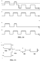
- FIG. 15 illustrates the CD circuit 1106 of Figure 13 with short detection circuit 1502 added thereto.
- This short detection circuit can detect a short created between WSS 102 and Vss via, for example, inadvertently activated high side current monitor 202R.
- the short detection circuit can detect the short in question in response to detecting a sudden drop in Hrep while Lrep is constant.
- the output of delta comparator 1302 and short detection circuit 1502 are provided as inputs to AND gate 1504.
- the output of AND gate 1504 is provided to signal select circuit 304 as shown.
- threshold compare circuit 306 will decode Hrep only when both short detection circuit 1502 and delta comparator 1302 assert their outputs. Otherwise, threshold compare circuit 306 will decode Lrep to produce WS1. It is noted that delta comparator 1302 and short detection circuit 1502 provide Flag1 and Flag1H, respectively, to ABS controller 114. Flag1 is described in U.S. Patent Application No. 16/055,554 . Flag1H, when asserted, indicates the existence of the short created by, for example, inadvertently activated current monitor 202R. ABS controller 114 may respond to an assertion of Flag1H by deactivating current monitor 202R.
- Figure 16 illustrates delta comparator 1302, AND gate 1504, and a more detailed view of an example short detection circuit 1502.
- short detection circuit 1502 includes compare circuits 1602 - 1612, each of which is configured to compare Hrep or Lrep to predetermined levels LV6, LV5 or LV3.
- LV6 and LV3 were described above.
- LV5 is selected to be a value below threshold value X.
- LV6, LV5 and LV3 are set to 10.5 mA, 9.5 mA, and 5.0 mA, respectively.
- compare circuit 1602 asserts its output only when Hrep exceeds 10.5 mA
- compare circuit 1604 asserts its output only when Lrep exceeds 10.5 mA
- compare circuit 1606 asserts its output only when Hrep exceeds 9.5 mA
- compare circuit 1508 asserts its output only when Lrep exceeds 9.5 mA
- compare circuit 1510 asserts its output only when Lrep exceeds 5.0 mA
- compare circuit 1612 asserts its output only one Hrep exceeds 5.0 mA.
- the outputs of compare circuits 1602-1612 are provided as inputs to AND gates 1614-1618 as shown.
- the inputs to AND gate 1616 are inverted.
- the outputs of AND gates 1616 and 1618 are provided as inputs to AND gate 1620.
- the outputs of AND gates 1614 and 1620 are provided as inputs to OR gate 1622.
- the output of OR gate 1622 and delta comparator 1302 are provided as inputs to AND gate 1504.
- the delta comparator 1302 shown in Figure 16 operates the same as the delta comparator 1302 shown in Figure 13 .
- the output of AND gate 1504 is used by signal selector 304 to select Hrep or Lrep for subsequent decoding to generate WS1.
- threshold detector 306 decodes Hrep to produce WS1.
- threshold detector 306 decodes Lrep to produce WS1.
- a method comprises transmitting a first current to a wheel speed sensor; receiving a second current from the wheel speed sensor; generating a wheel speed signal for output based on one of the first current or the second current.
- the wheel speed signal relates to a speed of a wheel that is associated with the wheel speed sensor.
- the wheel speed signal is generated based on the second current if magnitudes of the first and second currents exceed a first predetermined value, or if the magnitudes of the first and second currents exceed a second predetermined value while the first predetermined value exceeds the magnitudes of the first and second currents.
- the wheel speed signal is generated based on the first current if the first predetermined value exceeds the magnitude of the second current, or if the second predetermined value exceeds the magnitude of the second current.
- the method further comprises directly or indirectly comparing magnitudes of the first and second currents to the first predetermined value to determine whether the magnitudes of the first and second currents exceed the first predetermined value; and/or directly or indirectly comparing magnitudes of the first and second currents to determine whether the magnitudes of the first and second currents exceed the second predetermined value.
- the method further comprises setting a signal to a first state if the magnitudes of the first and second currents exceed the first predetermined value, or if the magnitudes of the first and second currents exceed the second predetermined value while the first predetermined value exceeds the magnitudes of the first and second currents; setting the signal to a second state if the first predetermined value exceeds the magnitude of the second current, or if the second predetermined value exceeds the magnitude of the second current.
- the method further comprises directly or indirectly comparing the magnitudes of the first and second currents.
- the wheel speed signal is generated based on the first current if the magnitude of the second current exceeds the magnitude of the first current by a predetermined amount.
- the method further comprises setting a signal to a first state if the magnitude of the first current exceeds the magnitude of the second current by the predetermined amount; setting the signal to a second state if the magnitude of the first current does not exceed the magnitude of the second current by the predetermined amount.
- the first current changes as teeth of a rotor pass the wheel speed sensor.
- the second current changes as teeth of the rotor pass the wheel speed sensor.
- the method further comprises generating a first voltage based on the first current.
- a magnitude of the first voltage is directly proportional to the magnitude of the first current; generating a second voltage based on the second current.
- a magnitude of the second voltage is directly proportional to the magnitude of the second current.
- the directly or indirectly comparing the magnitudes of the first and second currents to the first predetermined value comprises comparing the magnitudes of the first and second voltages to the first predetermined value.
- the directly or indirectly comparing the magnitudes of the first and second currents to the second predetermined value comprises comparing the first and second voltages to the second predetermined value.
- an apparatus which comprises a first circuit for transmitting a first current to a wheel speed sensor; a second circuit for receiving a second current from the wheel speed sensor; a circuit for generating a wheel speed signal for output based on the first current or the second current.
- the wheel speed signal relates to a speed of a wheel that is associated with the wheel speed sensor.
- the circuit generates the wheel speed signal based on the second current if the magnitudes of the first and second currents exceed a first predetermined value, or if the magnitudes of the first and second currents exceed a second predetermined value while the first predetermined value exceeds the magnitudes of the first and second currents.
- the circuit generates the wheel speed signal based on the first current if the first predetermined value exceeds the magnitude of the second current, or if the second predetermined value exceeds the magnitude of the second current.
- the apparatus further comprises a pair of first comparator circuits for directly or indirectly comparing magnitudes of the first and second currents, respectively, to the first predetermined value; a pair of second comparator circuits for directly or indirectly comparing magnitudes of the first and second currents, respectively, to a second predetermined value.
- the circuit is coupled to and configured to receive output signals from the pair of first comparator circuits and from the pair of second comparator circuits.
- the circuit is further configured to set a signal to a first state if the magnitudes of the first and second currents exceed the first predetermined value, or if the magnitudes of the first and second currents exceed the second predetermined value while the first predetermined value exceeds the magnitudes of the first and second currents; set the signal to a second state if the first predetermined value exceeds the magnitude of the second current, or if the second predetermined value exceeds the magnitude of the second current.
- the wheel speed signal is generated based on the first current if the magnitude of the second current exceeds the magnitude of the first current by predetermined amount.
- the circuit is configured to set a signal to a first state if the magnitude of the first current is greater than the magnitude of the second current by the predetermined amount.
- the circuit is configured to set a signal to a second state if the magnitude of the first current is not greater than the magnitude of the second current by the predetermined amount.
- the apparatus further comprises the wheel speed sensor.
- the wheel speed sensor is configured to vary the first and second currents as teeth of a rotor pass the wheel speed sensor.
- the circuit is further configured to generate a first voltage based on the first current.
- a magnitude of the first voltage is directly proportional to the magnitude of the first current.
- the circuit is further configured to generate a second voltage based on the second current.
- a magnitude of the second voltage is directly proportional to the magnitude of the second current.
- the circuit compares the magnitudes of the first and second currents to the first predetermined value by comparing the magnitudes of the first and second voltages to the first predetermined value.
- the circuit compares the magnitudes of the first and second currents to the second predetermined value by comparing the magnitudes of the first and second voltages to the second predetermined value.
- the circuit is configured to generate a wheel speed signal for output based on the first current or the second current.
- the wheel speed signal relates to a speed of a wheel that is associated with the wheel speed sensor.
- the circuit generates the wheel speed signal based on the second current if the magnitudes of the first and second currents exceed a first predetermined value, or if the magnitudes of the first and second currents exceed a second predetermined value while the first predetermined value exceeds the magnitudes of the first and second currents.
- the circuit generates the wheel speed signal based on the first current if the first predetermined value exceeds the magnitude of the second current, or if the second predetermined value exceeds the magnitude of the second current.
- the circuit is configured to directly or indirectly compares magnitudes of the first and second currents to the first predetermined value to determine whether the magnitudes of the first and second currents exceed the first predetermined value.
- the circuit is configured to directly or indirectly compares magnitudes of the first and second currents to determine whether the magnitudes of the first and second currents exceed the second predetermined value.
- the circuit is configured to set a signal to a first state if the magnitudes of the first and second currents exceed the first predetermined value, or if the magnitudes of the first and second currents exceed the second predetermined value while the first predetermined value exceeds the magnitudes of the first and second currents.
- the circuit is configured to set the signal to a second state if the first predetermined value exceeds the magnitude of the second current, or if the second predetermined value exceeds the magnitude of the second current.
- the apparatus further comprises the wheel speed sensor.
- the wheel speed sensor is configured to vary the first and second currents as teeth of a rotor pass the wheel speed sensor.
Landscapes
- Engineering & Computer Science (AREA)
- Physics & Mathematics (AREA)
- General Physics & Mathematics (AREA)
- Life Sciences & Earth Sciences (AREA)
- Sustainable Development (AREA)
- Sustainable Energy (AREA)
- Power Engineering (AREA)
- Transportation (AREA)
- Mechanical Engineering (AREA)
- Regulating Braking Force (AREA)
Claims (12)
- Verfahren zum Erfassen der Drehzahl eines Rads einschließlich Kurzschlusstoleranz, wobei das Verfahren umfasst:Übertragen eines ersten Stroms (IH) an einen Raddrehzahlsensor (102);Überwachen des ersten Stroms;Vergleichen der Größe des ersten Stroms mit einem ersten vorbestimmten Wert (LV6) und mit einem zweiten vorbestimmten Wert (LV3), der unter dem ersten vorbestimmten Wert liegt;Empfangen eines zweiten Stroms (IL) von dem Raddrehzahlsensor (102);Vergleichen der Größe des zweiten Stroms mit einem ersten vorbestimmten Wert (LV6) und mit einem zweiten vorbestimmten Wert (LV3);Überwachen des zweiten Stroms;Erzeugen eines Raddrehzahlsignals (WS1) zur Ausgabe auf Basis eines des ersten Stroms (IH) oder des zweiten Stroms (IL), wobei das Raddrehzahlsignal (WS1) zu einer Drehzahl eines Rads in Beziehung steht, das mit dem Raddrehzahlsensor (102) assoziiert ist;dadurch gekennzeichnet, dass das Raddrehzahlsignal (WS1) auf Basis des zweiten Stroms (IL) als Reaktion darauf erzeugt wird, dass entweder die Größen jedes des ersten und zweiten Stroms (IH, IL) den ersten vorbestimmten Wert (LV6) übersteigen oder die Größe des zweiten Stroms (IL) den zweiten vorbestimmten Wert (LV3) übersteigt und der erste vorbestimmte Wert (LV6) die Größen des ersten und zweiten Stroms (IH, IL) übersteigt; unddas Raddrehzahlsignal (WS1) auf Basis des ersten Stroms (IH) als Reaktion darauf erzeugt wird, dass entweder der erste vorbestimmte Wert (LV6) die Größe des zweiten Stroms (IL) übersteigt oder der zweite vorbestimmte Wert (LV3) die Größe des zweiten Stroms (IL) übersteigt.
- Verfahren nach Anspruch 1, weiter umfassend:Vergleichen der Größen des ersten und zweiten Stroms (IH, IL);wobei das Raddrehzahlsignal (WS1) auf Basis des ersten Stroms (IH) erzeugt wird, falls die Größe des zweiten Stroms (IL) die Größe des ersten Stroms (IH) um ein vorbestimmtes Ausmaß übersteigt.
- Verfahren nach Anspruch 2, weiter umfassend:Setzen eines Signals (SELECT) auf einen ersten Zustand, falls die Größe des ersten Stroms (IH) die Größe des zweiten Stroms (IL) um das vorbestimmte Ausmaß übersteigt;Setzen des Signals (SELECT) auf einen zweiten Zustand, falls die Größe des ersten Stroms (IH) die Größe des zweiten Stroms (IL) nicht um das vorbestimmte Ausmaß übersteigt.
- Verfahren nach einem der Ansprüche 1 bis 3:
wobei jeder des ersten Stroms (IH) und des zweiten Stroms (IL) sich ändern, während Zähne eines Rotors (104) den Raddrehzahlsensor (102) passieren. - Verfahren nach einem der Ansprüche 2 bis 6, weiter umfassend:Erzeugen einer ersten Spannung auf Basis des ersten Stroms (IH), wobei eine Größe der ersten Spannung zu der Größe des ersten Stroms (IH) direkt proportional ist;Erzeugen einer zweiten Spannung auf Basis des zweiten Stroms (IL), wobei eine Größe der zweiten Spannung zu der Größe des zweiten Stroms (IL) direkt proportional ist;wobei das Vergleichen der Größen des ersten und zweiten Stroms (IH, IL) mit dem ersten vorbestimmten Wert (LV6) das Vergleichen der Größen der ersten und zweiten Spannung mit dem ersten vorbestimmten Wert (LV6) umfasst;wobei das Vergleichen der Größe des ersten und zweiten Stroms (IH, IL) mit dem zweiten vorbestimmten Wert (LV3) das Vergleichen der ersten und zweiten Spannung mit dem zweiten vorbestimmten Wert (LV3) umfasst.
- Kurzschlusstolerante Raddrehzahlerfassungsvorrichtung, umfassend:eine erste Schaltung (202), die ausgelegt ist zum Übertragen eines ersten Stroms (IH) zu einem Raddrehzahlsensor (102);eine zweite Schaltung (204), die ausgelegt ist zum Empfangen eines zweiten Stroms (IL) von dem Raddrehzahlsignal (102);eine Schaltung (206), die ausgelegt ist zum Erzeugen eines Raddrehzahlsignals (WS1) zur Ausgabe auf Basis des ersten Stroms (IH) oder des zweiten Stroms (IL), wobei das Raddrehzahlsignal (WS1) zu einer Drehzahl eines Rads in Beziehung steht, das mit dem Raddrehzahlsensor (102) assoziiert ist;dadurch gekennzeichnet, dass die Schaltung (206) ausgelegt ist zum Erzeugen des Raddrehzahlsignals (WS1) auf Basis des zweiten Stroms (IL), falls die Größen des ersten und zweiten Stroms (IH, IL) einen ersten vorbestimmten Wert (LV6) übersteigen, oder falls die Größen des ersten und zweiten Stroms (IH, IL) einen zweiten vorbestimmten Wert (LV3) übersteigen, während der erste vorbestimmte Wert (LV6) die Größen des ersten und zweiten Stroms (IH, IL) übersteigt;und die Schaltung (206) ausgelegt ist zum Erzeugen des Raddrehzahlsignals (WS1) auf Basis des ersten Stroms (IH), falls der erste vorbestimmte Wert (LV6) die Größe des zweiten Stroms (IL) übersteigt, oder falls der zweite vorbestimmte Wert (LV3) die Größe des zweiten Stroms (IL) übersteigt.
- Vorrichtung nach Anspruch 6, wobei die Schaltung (206) umfasst:ein Paar von ersten Vergleicherschaltungen (1002, 1004), die ausgelegt sind zum Vergleichen von Größen jeweils des ersten und zweiten Stroms (IH, IL) mit dem ersten vorbestimmten Wert (LV6);ein Paar von zweiten Vergleicherschaltungen (1006, 1008), die ausgelegt sind zum Vergleichen jeweils von Größen des ersten und zweiten Stroms (IH, IL) mit einem zweiten vorbestimmten Wert (LV3);wobei die Schaltung (206) gekoppelt ist an und ausgelegt ist zum Empfangen von Ausgangssignalen von dem Paar von ersten Vergleicherschaltungen und von dem Paar von zweiten Vergleicherschaltungen.
- Vorrichtung nach Anspruch 6 oder Anspruch 7, wobei die Schaltung (206) weiter ausgelegt ist zum:Setzen eines Signals (SELECT) auf einen ersten Zustand, falls die Größen des ersten und zweiten Stroms (IH, IL) den ersten vorbestimmten Wert (LV6) übersteigen, oder falls die Größen des ersten und zweiten Stroms (IH, IL) den zweiten vorbestimmten Wert (LV3) übersteigen, während der erste vorbestimmte Wert (LV6) die Größen des ersten und zweiten Stroms (IH, IL) übersteigt;Setzen des Signals (SELECT) auf einen zweiten Zustand, falls der erste vorbestimmte Wert (LV6) die Größe des zweiten Stroms (IL) übersteigt, oder falls der zweite vorbestimmte Wert (LV3) die Größe des zweiten Stroms (IL) übersteigt.
- Vorrichtung nach einem der Ansprüche 6 bis 8, wobei die Schaltung (206) einen Vergleicher (302) umfasst, der derart ausgelegt ist, dass das Raddrehzahlsignal (WS1) auf Basis des ersten Stroms (IH) erzeugt wird, falls die Größe des zweiten Stroms (IL) die Größe des ersten Stroms (IH) um ein vorbestimmtes Ausmaß übersteigt.
- Vorrichtung nach Anspruch 8:wobei die Schaltung (206) ausgelegt ist zum Setzen eines Signals auf einen ersten Zustand, falls die Größe des ersten Stroms (IH) um das vorbestimmte Ausmaß größer ist als die Größe des zweiten Stroms (IL);wobei die Schaltung (206) ausgelegt ist zum Setzen eines Signals auf einen zweiten Zustand, falls die Größe des ersten Stroms (IH) nicht um das vorbestimmte Ausmaß größer ist als die Größe des zweiten Stroms (IL).
- Vorrichtung nach einem der Ansprüche 6 bis 10, weiter umfassend den Raddrehzahlsensor (102), wobei der Raddrehzahlsensor (102) ausgelegt ist zum Variieren des ersten und zweiten Stroms (IH, IL), während Zähne eines Rotors (104) den Raddrehzahlsensor (102) passieren.
- Vorrichtung nach einem der Ansprüche 7 bis 11:wobei die Schaltung (206) weiter ausgelegt ist zum Erzeugen einer ersten Spannung auf Basis des ersten Stroms (IH), wobei eine Größe der ersten Spannung zu der Größe des ersten Stroms (IH) direkt proportional ist;wobei die Schaltung (206) weiter ausgelegt ist zum Erzeugen einer zweiten Spannung auf Basis des zweiten Stroms (IL), wenn eine Größe der zweiten Spannung zu der Größe des zweiten Stroms (IL) direkt proportional ist;wobei die Schaltung (206) ausgelegt ist zum Vergleichen der Größen des ersten und zweiten Stroms (IH, IL) mit dem ersten vorbestimmten Wert (LV6) durch Vergleichen der Größen der ersten und zweiten Spannung mit dem ersten vorbestimmten Wert (LV6);wobei die Schaltung (206) ausgelegt ist zum Vergleichen der Größen des ersten und zweiten Stroms (IH, IL) mit dem zweiten vorbestimmten Wert (LV3) durch Vergleichen der Größen der ersten und zweiten Spannung mit dem zweiten vorbestimmten Wert (LV3).
Priority Applications (2)
| Application Number | Priority Date | Filing Date | Title |
|---|---|---|---|
| EP19305029.1A EP3680122B1 (de) | 2019-01-09 | 2019-01-09 | Kurzschlussfestigkeit eines begleiterchips |
| US16/276,960 US10890598B2 (en) | 2019-01-09 | 2019-02-15 | Companion chip short circuit immunity |
Applications Claiming Priority (1)
| Application Number | Priority Date | Filing Date | Title |
|---|---|---|---|
| EP19305029.1A EP3680122B1 (de) | 2019-01-09 | 2019-01-09 | Kurzschlussfestigkeit eines begleiterchips |
Publications (2)
| Publication Number | Publication Date |
|---|---|
| EP3680122A1 EP3680122A1 (de) | 2020-07-15 |
| EP3680122B1 true EP3680122B1 (de) | 2022-08-31 |
Family
ID=65200750
Family Applications (1)
| Application Number | Title | Priority Date | Filing Date |
|---|---|---|---|
| EP19305029.1A Active EP3680122B1 (de) | 2019-01-09 | 2019-01-09 | Kurzschlussfestigkeit eines begleiterchips |
Country Status (2)
| Country | Link |
|---|---|
| US (1) | US10890598B2 (de) |
| EP (1) | EP3680122B1 (de) |
Families Citing this family (3)
| Publication number | Priority date | Publication date | Assignee | Title |
|---|---|---|---|---|
| DE102020205961A1 (de) * | 2019-11-06 | 2021-05-06 | Robert Bosch Gesellschaft mit beschränkter Haftung | Sensoranordnung für ein Fahrzeug und mehrkreisiges Bremssystem |
| EP3993249A1 (de) * | 2020-10-28 | 2022-05-04 | NXP USA, Inc. | Netzteil zur gewährleistung des sicheren verhaltens einer wechselrichteranwendung |
| KR102810145B1 (ko) * | 2023-06-02 | 2025-05-20 | 에이치엘만도 주식회사 | 브레이크 장치 및 그 제어 방법 |
Citations (1)
| Publication number | Priority date | Publication date | Assignee | Title |
|---|---|---|---|---|
| US20100182725A1 (en) * | 2005-08-10 | 2010-07-22 | Continental Teves Ag & Co. Ohg | Circuit Arrangement and Method for Monitoring Wheel Speed Sensors in a Motor Vehicle Control Device |
Family Cites Families (14)
| Publication number | Priority date | Publication date | Assignee | Title |
|---|---|---|---|---|
| US5406485A (en) | 1993-11-09 | 1995-04-11 | Delco Electronics Corp. | Method and apparatus for detecting faulty operation of a wheel speed sensor |
| US5404304A (en) | 1993-11-19 | 1995-04-04 | Delco Electronics Corporation | Vehicle control system for determining verified wheel speed signals |
| US5493214A (en) * | 1994-02-22 | 1996-02-20 | Delco Electronics Corporation | Fault detection scheme for a variable reluctance sensor interface having a differential input and adaptive control |
| DE19618867A1 (de) | 1995-08-26 | 1997-02-27 | Bosch Gmbh Robert | System zur Veränderung eines Drehzahlsignals |
| DE19602243A1 (de) | 1996-01-23 | 1997-07-24 | Teves Gmbh Alfred | Schaltungsanordnung zur Anpassung eines aktiven Sensors an eine Auswerteschaltung |
| DE19635440B4 (de) | 1996-08-31 | 2005-07-21 | Robert Bosch Gmbh | Verfahren und Vorrichtung zur Überwachung wenigstens eines Sensors |
| WO1999001774A1 (de) | 1997-07-02 | 1999-01-14 | Siemens Aktiengesellschaft | Diagnoseeinrichtung zur erkennung von fehlschlüssen bei einem induktiven sensor |
| DE10103853B4 (de) | 2001-01-30 | 2010-03-18 | Wabco Gmbh | Verfahren zur Ansteuerung einer Warnlampe bei einem Antiblockiersystem für Strassenfahrzeuge |
| EP1356975B1 (de) * | 2002-04-23 | 2009-12-16 | Jtekt Corporation | Momentenverteilungs- Steuerungsgerät für vierradgetriebenes Fahrzeug |
| US7520573B2 (en) | 2005-12-22 | 2009-04-21 | Kelsey-Hayes Company | Shadow zone fault detection |
| JP6201366B2 (ja) | 2013-03-27 | 2017-09-27 | 株式会社ジェイテクト | 電気負荷制御装置の過電流異常判定装置、駆動力配分制御装置、および過電流異常判定方法ならびに過電流異常判定プログラム |
| US9733295B2 (en) * | 2014-12-02 | 2017-08-15 | Nxp Usa, Inc. | Sensor circuit, vehicle and method therefor |
| WO2017110010A1 (ja) | 2015-12-21 | 2017-06-29 | パナソニックIpマネジメント株式会社 | 電動車両の速度制御装置 |
| KR102454021B1 (ko) * | 2016-04-15 | 2022-10-14 | 현대모비스 주식회사 | 휠센서 인터페이스 장치 |
-
2019
- 2019-01-09 EP EP19305029.1A patent/EP3680122B1/de active Active
- 2019-02-15 US US16/276,960 patent/US10890598B2/en active Active
Patent Citations (1)
| Publication number | Priority date | Publication date | Assignee | Title |
|---|---|---|---|---|
| US20100182725A1 (en) * | 2005-08-10 | 2010-07-22 | Continental Teves Ag & Co. Ohg | Circuit Arrangement and Method for Monitoring Wheel Speed Sensors in a Motor Vehicle Control Device |
Also Published As
| Publication number | Publication date |
|---|---|
| US10890598B2 (en) | 2021-01-12 |
| US20200217870A1 (en) | 2020-07-09 |
| EP3680122A1 (de) | 2020-07-15 |
Similar Documents
| Publication | Publication Date | Title |
|---|---|---|
| US6492804B2 (en) | Detected signal processing device for rotating sensor and detected signal outputting method therefor | |
| EP1226061B1 (de) | Verfahren und vorrichtung zum testen der funktion eines motors und seiner treiberschaltung | |
| EP3708967B1 (de) | Motordrehwinkeldetektionsvorrichtung und elektrische servolenkvorrichtung mit der motordrehwinkeldetektionsvorrichtung | |
| US5648759A (en) | Failsafe voltage regulator with warning signal driver | |
| US8434583B2 (en) | Electric power steering system | |
| EP3680122A1 (de) | Kurzschlussfestigkeit eines begleiterchips | |
| US20010053952A1 (en) | Diagnostic apparatus and method for motor driven power-assisted steering system | |
| JPH0353140B2 (de) | ||
| US6111514A (en) | Solenoid fail-safe using current feedback as a diagnostic input | |
| CN107300626B (zh) | 车轮传感器接口装置 | |
| US5372410A (en) | Anti-lock braking system | |
| US9720024B2 (en) | Sensor circuit, vehicle and method therefor | |
| EP3590776B1 (de) | Resistive kurzschlussfestigkeit für raddrehzahlsensorschnittstelle am bremssystem | |
| JP2001312318A (ja) | 複数電源回路を備えた電子制御装置 | |
| US12413140B2 (en) | Power converter and control method for power converter | |
| JPH1144701A (ja) | 車輪速計測装置 | |
| US6486626B1 (en) | Apparatus and a method for controlling an electric vehicle | |
| JP2014102205A (ja) | センサ装置 | |
| KR101522032B1 (ko) | 차량의 휠속도 오류 검출장치 | |
| JP3191436B2 (ja) | 負荷駆動系の監視装置 | |
| KR100376967B1 (ko) | 차륜속도 감지장치 | |
| CN118613663A (zh) | 用于有源转速传感器的操控电路 | |
| EP0742919A1 (de) | Sicherheitstaktgeber für schlupfgeregelte bremsanlagen | |
| JPS62286874A (ja) | 電動式パワ−ステアリング装置 | |
| JPH09318641A (ja) | 回転センサの異常検出装置 |
Legal Events
| Date | Code | Title | Description |
|---|---|---|---|
| PUAI | Public reference made under article 153(3) epc to a published international application that has entered the european phase |
Free format text: ORIGINAL CODE: 0009012 |
|
| STAA | Information on the status of an ep patent application or granted ep patent |
Free format text: STATUS: THE APPLICATION HAS BEEN PUBLISHED |
|
| AK | Designated contracting states |
Kind code of ref document: A1 Designated state(s): AL AT BE BG CH CY CZ DE DK EE ES FI FR GB GR HR HU IE IS IT LI LT LU LV MC MK MT NL NO PL PT RO RS SE SI SK SM TR |
|
| AX | Request for extension of the european patent |
Extension state: BA ME |
|
| STAA | Information on the status of an ep patent application or granted ep patent |
Free format text: STATUS: REQUEST FOR EXAMINATION WAS MADE |
|
| 17P | Request for examination filed |
Effective date: 20210115 |
|
| RBV | Designated contracting states (corrected) |
Designated state(s): AL AT BE BG CH CY CZ DE DK EE ES FI FR GB GR HR HU IE IS IT LI LT LU LV MC MK MT NL NO PL PT RO RS SE SI SK SM TR |
|
| GRAP | Despatch of communication of intention to grant a patent |
Free format text: ORIGINAL CODE: EPIDOSNIGR1 |
|
| STAA | Information on the status of an ep patent application or granted ep patent |
Free format text: STATUS: GRANT OF PATENT IS INTENDED |
|
| INTG | Intention to grant announced |
Effective date: 20220113 |
|
| GRAJ | Information related to disapproval of communication of intention to grant by the applicant or resumption of examination proceedings by the epo deleted |
Free format text: ORIGINAL CODE: EPIDOSDIGR1 |
|
| STAA | Information on the status of an ep patent application or granted ep patent |
Free format text: STATUS: REQUEST FOR EXAMINATION WAS MADE |
|
| INTC | Intention to grant announced (deleted) | ||
| GRAP | Despatch of communication of intention to grant a patent |
Free format text: ORIGINAL CODE: EPIDOSNIGR1 |
|
| STAA | Information on the status of an ep patent application or granted ep patent |
Free format text: STATUS: GRANT OF PATENT IS INTENDED |
|
| GRAS | Grant fee paid |
Free format text: ORIGINAL CODE: EPIDOSNIGR3 |
|
| GRAA | (expected) grant |
Free format text: ORIGINAL CODE: 0009210 |
|
| STAA | Information on the status of an ep patent application or granted ep patent |
Free format text: STATUS: THE PATENT HAS BEEN GRANTED |
|
| INTG | Intention to grant announced |
Effective date: 20220718 |
|
| AK | Designated contracting states |
Kind code of ref document: B1 Designated state(s): AL AT BE BG CH CY CZ DE DK EE ES FI FR GB GR HR HU IE IS IT LI LT LU LV MC MK MT NL NO PL PT RO RS SE SI SK SM TR |
|
| REG | Reference to a national code |
Ref country code: CH Ref legal event code: EP Ref country code: GB Ref legal event code: FG4D |
|
| REG | Reference to a national code |
Ref country code: AT Ref legal event code: REF Ref document number: 1515051 Country of ref document: AT Kind code of ref document: T Effective date: 20220915 Ref country code: DE Ref legal event code: R096 Ref document number: 602019018922 Country of ref document: DE |
|
| REG | Reference to a national code |
Ref country code: IE Ref legal event code: FG4D |
|
| REG | Reference to a national code |
Ref country code: LT Ref legal event code: MG9D |
|
| REG | Reference to a national code |
Ref country code: NL Ref legal event code: MP Effective date: 20220831 |
|
| PG25 | Lapsed in a contracting state [announced via postgrant information from national office to epo] |
Ref country code: SE Free format text: LAPSE BECAUSE OF FAILURE TO SUBMIT A TRANSLATION OF THE DESCRIPTION OR TO PAY THE FEE WITHIN THE PRESCRIBED TIME-LIMIT Effective date: 20220831 Ref country code: RS Free format text: LAPSE BECAUSE OF FAILURE TO SUBMIT A TRANSLATION OF THE DESCRIPTION OR TO PAY THE FEE WITHIN THE PRESCRIBED TIME-LIMIT Effective date: 20220831 Ref country code: NO Free format text: LAPSE BECAUSE OF FAILURE TO SUBMIT A TRANSLATION OF THE DESCRIPTION OR TO PAY THE FEE WITHIN THE PRESCRIBED TIME-LIMIT Effective date: 20221130 Ref country code: LV Free format text: LAPSE BECAUSE OF FAILURE TO SUBMIT A TRANSLATION OF THE DESCRIPTION OR TO PAY THE FEE WITHIN THE PRESCRIBED TIME-LIMIT Effective date: 20220831 Ref country code: LT Free format text: LAPSE BECAUSE OF FAILURE TO SUBMIT A TRANSLATION OF THE DESCRIPTION OR TO PAY THE FEE WITHIN THE PRESCRIBED TIME-LIMIT Effective date: 20220831 Ref country code: FI Free format text: LAPSE BECAUSE OF FAILURE TO SUBMIT A TRANSLATION OF THE DESCRIPTION OR TO PAY THE FEE WITHIN THE PRESCRIBED TIME-LIMIT Effective date: 20220831 |
|
| REG | Reference to a national code |
Ref country code: AT Ref legal event code: MK05 Ref document number: 1515051 Country of ref document: AT Kind code of ref document: T Effective date: 20220831 |
|
| PG25 | Lapsed in a contracting state [announced via postgrant information from national office to epo] |
Ref country code: PL Free format text: LAPSE BECAUSE OF FAILURE TO SUBMIT A TRANSLATION OF THE DESCRIPTION OR TO PAY THE FEE WITHIN THE PRESCRIBED TIME-LIMIT Effective date: 20220831 Ref country code: IS Free format text: LAPSE BECAUSE OF FAILURE TO SUBMIT A TRANSLATION OF THE DESCRIPTION OR TO PAY THE FEE WITHIN THE PRESCRIBED TIME-LIMIT Effective date: 20221231 Ref country code: HR Free format text: LAPSE BECAUSE OF FAILURE TO SUBMIT A TRANSLATION OF THE DESCRIPTION OR TO PAY THE FEE WITHIN THE PRESCRIBED TIME-LIMIT Effective date: 20220831 Ref country code: GR Free format text: LAPSE BECAUSE OF FAILURE TO SUBMIT A TRANSLATION OF THE DESCRIPTION OR TO PAY THE FEE WITHIN THE PRESCRIBED TIME-LIMIT Effective date: 20221201 |
|
| PG25 | Lapsed in a contracting state [announced via postgrant information from national office to epo] |
Ref country code: SM Free format text: LAPSE BECAUSE OF FAILURE TO SUBMIT A TRANSLATION OF THE DESCRIPTION OR TO PAY THE FEE WITHIN THE PRESCRIBED TIME-LIMIT Effective date: 20220831 Ref country code: RO Free format text: LAPSE BECAUSE OF FAILURE TO SUBMIT A TRANSLATION OF THE DESCRIPTION OR TO PAY THE FEE WITHIN THE PRESCRIBED TIME-LIMIT Effective date: 20220831 Ref country code: PT Free format text: LAPSE BECAUSE OF FAILURE TO SUBMIT A TRANSLATION OF THE DESCRIPTION OR TO PAY THE FEE WITHIN THE PRESCRIBED TIME-LIMIT Effective date: 20230102 Ref country code: ES Free format text: LAPSE BECAUSE OF FAILURE TO SUBMIT A TRANSLATION OF THE DESCRIPTION OR TO PAY THE FEE WITHIN THE PRESCRIBED TIME-LIMIT Effective date: 20220831 Ref country code: DK Free format text: LAPSE BECAUSE OF FAILURE TO SUBMIT A TRANSLATION OF THE DESCRIPTION OR TO PAY THE FEE WITHIN THE PRESCRIBED TIME-LIMIT Effective date: 20220831 Ref country code: CZ Free format text: LAPSE BECAUSE OF FAILURE TO SUBMIT A TRANSLATION OF THE DESCRIPTION OR TO PAY THE FEE WITHIN THE PRESCRIBED TIME-LIMIT Effective date: 20220831 Ref country code: AT Free format text: LAPSE BECAUSE OF FAILURE TO SUBMIT A TRANSLATION OF THE DESCRIPTION OR TO PAY THE FEE WITHIN THE PRESCRIBED TIME-LIMIT Effective date: 20220831 |
|
| PG25 | Lapsed in a contracting state [announced via postgrant information from national office to epo] |
Ref country code: SK Free format text: LAPSE BECAUSE OF FAILURE TO SUBMIT A TRANSLATION OF THE DESCRIPTION OR TO PAY THE FEE WITHIN THE PRESCRIBED TIME-LIMIT Effective date: 20220831 Ref country code: EE Free format text: LAPSE BECAUSE OF FAILURE TO SUBMIT A TRANSLATION OF THE DESCRIPTION OR TO PAY THE FEE WITHIN THE PRESCRIBED TIME-LIMIT Effective date: 20220831 |
|
| REG | Reference to a national code |
Ref country code: DE Ref legal event code: R097 Ref document number: 602019018922 Country of ref document: DE |
|
| PG25 | Lapsed in a contracting state [announced via postgrant information from national office to epo] |
Ref country code: NL Free format text: LAPSE BECAUSE OF FAILURE TO SUBMIT A TRANSLATION OF THE DESCRIPTION OR TO PAY THE FEE WITHIN THE PRESCRIBED TIME-LIMIT Effective date: 20220831 Ref country code: AL Free format text: LAPSE BECAUSE OF FAILURE TO SUBMIT A TRANSLATION OF THE DESCRIPTION OR TO PAY THE FEE WITHIN THE PRESCRIBED TIME-LIMIT Effective date: 20220831 |
|
| PLBE | No opposition filed within time limit |
Free format text: ORIGINAL CODE: 0009261 |
|
| STAA | Information on the status of an ep patent application or granted ep patent |
Free format text: STATUS: NO OPPOSITION FILED WITHIN TIME LIMIT |
|
| 26N | No opposition filed |
Effective date: 20230601 |
|
| P01 | Opt-out of the competence of the unified patent court (upc) registered |
Effective date: 20230725 |
|
| PG25 | Lapsed in a contracting state [announced via postgrant information from national office to epo] |
Ref country code: SI Free format text: LAPSE BECAUSE OF FAILURE TO SUBMIT A TRANSLATION OF THE DESCRIPTION OR TO PAY THE FEE WITHIN THE PRESCRIBED TIME-LIMIT Effective date: 20220831 |
|
| REG | Reference to a national code |
Ref country code: CH Ref legal event code: PL |
|
| PG25 | Lapsed in a contracting state [announced via postgrant information from national office to epo] |
Ref country code: LU Free format text: LAPSE BECAUSE OF NON-PAYMENT OF DUE FEES Effective date: 20230109 |
|
| REG | Reference to a national code |
Ref country code: BE Ref legal event code: MM Effective date: 20230131 |
|
| PG25 | Lapsed in a contracting state [announced via postgrant information from national office to epo] |
Ref country code: LI Free format text: LAPSE BECAUSE OF NON-PAYMENT OF DUE FEES Effective date: 20230131 Ref country code: CH Free format text: LAPSE BECAUSE OF NON-PAYMENT OF DUE FEES Effective date: 20230131 |
|
| PG25 | Lapsed in a contracting state [announced via postgrant information from national office to epo] |
Ref country code: FR Free format text: LAPSE BECAUSE OF NON-PAYMENT OF DUE FEES Effective date: 20230131 Ref country code: BE Free format text: LAPSE BECAUSE OF NON-PAYMENT OF DUE FEES Effective date: 20230131 |
|
| PG25 | Lapsed in a contracting state [announced via postgrant information from national office to epo] |
Ref country code: IE Free format text: LAPSE BECAUSE OF NON-PAYMENT OF DUE FEES Effective date: 20230109 |
|
| PG25 | Lapsed in a contracting state [announced via postgrant information from national office to epo] |
Ref country code: IT Free format text: LAPSE BECAUSE OF FAILURE TO SUBMIT A TRANSLATION OF THE DESCRIPTION OR TO PAY THE FEE WITHIN THE PRESCRIBED TIME-LIMIT Effective date: 20220831 |
|
| PG25 | Lapsed in a contracting state [announced via postgrant information from national office to epo] |
Ref country code: MC Free format text: LAPSE BECAUSE OF FAILURE TO SUBMIT A TRANSLATION OF THE DESCRIPTION OR TO PAY THE FEE WITHIN THE PRESCRIBED TIME-LIMIT Effective date: 20220831 |
|
| PG25 | Lapsed in a contracting state [announced via postgrant information from national office to epo] |
Ref country code: MC Free format text: LAPSE BECAUSE OF FAILURE TO SUBMIT A TRANSLATION OF THE DESCRIPTION OR TO PAY THE FEE WITHIN THE PRESCRIBED TIME-LIMIT Effective date: 20220831 |
|
| PG25 | Lapsed in a contracting state [announced via postgrant information from national office to epo] |
Ref country code: BG Free format text: LAPSE BECAUSE OF FAILURE TO SUBMIT A TRANSLATION OF THE DESCRIPTION OR TO PAY THE FEE WITHIN THE PRESCRIBED TIME-LIMIT Effective date: 20220831 |
|
| PG25 | Lapsed in a contracting state [announced via postgrant information from national office to epo] |
Ref country code: BG Free format text: LAPSE BECAUSE OF FAILURE TO SUBMIT A TRANSLATION OF THE DESCRIPTION OR TO PAY THE FEE WITHIN THE PRESCRIBED TIME-LIMIT Effective date: 20220831 |
|
| PG25 | Lapsed in a contracting state [announced via postgrant information from national office to epo] |
Ref country code: CY Free format text: LAPSE BECAUSE OF FAILURE TO SUBMIT A TRANSLATION OF THE DESCRIPTION OR TO PAY THE FEE WITHIN THE PRESCRIBED TIME-LIMIT; INVALID AB INITIO Effective date: 20190109 |
|
| PG25 | Lapsed in a contracting state [announced via postgrant information from national office to epo] |
Ref country code: HU Free format text: LAPSE BECAUSE OF FAILURE TO SUBMIT A TRANSLATION OF THE DESCRIPTION OR TO PAY THE FEE WITHIN THE PRESCRIBED TIME-LIMIT; INVALID AB INITIO Effective date: 20190109 |
|
| PG25 | Lapsed in a contracting state [announced via postgrant information from national office to epo] |
Ref country code: TR Free format text: LAPSE BECAUSE OF FAILURE TO SUBMIT A TRANSLATION OF THE DESCRIPTION OR TO PAY THE FEE WITHIN THE PRESCRIBED TIME-LIMIT Effective date: 20220831 |
|
| PGFP | Annual fee paid to national office [announced via postgrant information from national office to epo] |
Ref country code: GB Payment date: 20251220 Year of fee payment: 8 |
|
| PGFP | Annual fee paid to national office [announced via postgrant information from national office to epo] |
Ref country code: DE Payment date: 20251217 Year of fee payment: 8 |