EP3680261B1 - Polymer, beschichtungszusammensetzung damit und organisches lichtemittierendes element damit - Google Patents
Polymer, beschichtungszusammensetzung damit und organisches lichtemittierendes element damit Download PDFInfo
- Publication number
- EP3680261B1 EP3680261B1 EP19760366.5A EP19760366A EP3680261B1 EP 3680261 B1 EP3680261 B1 EP 3680261B1 EP 19760366 A EP19760366 A EP 19760366A EP 3680261 B1 EP3680261 B1 EP 3680261B1
- Authority
- EP
- European Patent Office
- Prior art keywords
- group
- substituted
- unsubstituted
- polymer
- present specification
- Prior art date
- Legal status (The legal status is an assumption and is not a legal conclusion. Google has not performed a legal analysis and makes no representation as to the accuracy of the status listed.)
- Active
Links
Images
Classifications
-
- C—CHEMISTRY; METALLURGY
- C08—ORGANIC MACROMOLECULAR COMPOUNDS; THEIR PREPARATION OR CHEMICAL WORKING-UP; COMPOSITIONS BASED THEREON
- C08F—MACROMOLECULAR COMPOUNDS OBTAINED BY REACTIONS ONLY INVOLVING CARBON-TO-CARBON UNSATURATED BONDS
- C08F212/00—Copolymers of compounds having one or more unsaturated aliphatic radicals, each having only one carbon-to-carbon double bond, and at least one being terminated by an aromatic carbocyclic ring
- C08F212/02—Monomers containing only one unsaturated aliphatic radical
- C08F212/04—Monomers containing only one unsaturated aliphatic radical containing one ring
- C08F212/14—Monomers containing only one unsaturated aliphatic radical containing one ring substituted by heteroatoms or groups containing heteroatoms
- C08F212/26—Nitrogen
-
- C—CHEMISTRY; METALLURGY
- C08—ORGANIC MACROMOLECULAR COMPOUNDS; THEIR PREPARATION OR CHEMICAL WORKING-UP; COMPOSITIONS BASED THEREON
- C08F—MACROMOLECULAR COMPOUNDS OBTAINED BY REACTIONS ONLY INVOLVING CARBON-TO-CARBON UNSATURATED BONDS
- C08F212/00—Copolymers of compounds having one or more unsaturated aliphatic radicals, each having only one carbon-to-carbon double bond, and at least one being terminated by an aromatic carbocyclic ring
- C08F212/02—Monomers containing only one unsaturated aliphatic radical
- C08F212/04—Monomers containing only one unsaturated aliphatic radical containing one ring
- C08F212/14—Monomers containing only one unsaturated aliphatic radical containing one ring substituted by heteroatoms or groups containing heteroatoms
-
- C—CHEMISTRY; METALLURGY
- C08—ORGANIC MACROMOLECULAR COMPOUNDS; THEIR PREPARATION OR CHEMICAL WORKING-UP; COMPOSITIONS BASED THEREON
- C08F—MACROMOLECULAR COMPOUNDS OBTAINED BY REACTIONS ONLY INVOLVING CARBON-TO-CARBON UNSATURATED BONDS
- C08F212/00—Copolymers of compounds having one or more unsaturated aliphatic radicals, each having only one carbon-to-carbon double bond, and at least one being terminated by an aromatic carbocyclic ring
- C08F212/02—Monomers containing only one unsaturated aliphatic radical
- C08F212/32—Monomers containing only one unsaturated aliphatic radical containing two or more rings
-
- C—CHEMISTRY; METALLURGY
- C09—DYES; PAINTS; POLISHES; NATURAL RESINS; ADHESIVES; COMPOSITIONS NOT OTHERWISE PROVIDED FOR; APPLICATIONS OF MATERIALS NOT OTHERWISE PROVIDED FOR
- C09D—COATING COMPOSITIONS, e.g. PAINTS, VARNISHES OR LACQUERS; FILLING PASTES; CHEMICAL PAINT OR INK REMOVERS; INKS; CORRECTING FLUIDS; WOODSTAINS; PASTES OR SOLIDS FOR COLOURING OR PRINTING; USE OF MATERIALS THEREFOR
- C09D125/00—Coating compositions based on homopolymers or copolymers of compounds having one or more unsaturated aliphatic radicals, each having only one carbon-to-carbon double bond, and at least one being terminated by an aromatic carbocyclic ring; Coating compositions based on derivatives of such polymers
- C09D125/18—Homopolymers or copolymers of aromatic monomers containing elements other than carbon and hydrogen
-
- C—CHEMISTRY; METALLURGY
- C09—DYES; PAINTS; POLISHES; NATURAL RESINS; ADHESIVES; COMPOSITIONS NOT OTHERWISE PROVIDED FOR; APPLICATIONS OF MATERIALS NOT OTHERWISE PROVIDED FOR
- C09D—COATING COMPOSITIONS, e.g. PAINTS, VARNISHES OR LACQUERS; FILLING PASTES; CHEMICAL PAINT OR INK REMOVERS; INKS; CORRECTING FLUIDS; WOODSTAINS; PASTES OR SOLIDS FOR COLOURING OR PRINTING; USE OF MATERIALS THEREFOR
- C09D5/00—Coating compositions, e.g. paints, varnishes or lacquers, characterised by their physical nature or the effects produced; Filling pastes
- C09D5/24—Electrically-conducting paints
-
- C—CHEMISTRY; METALLURGY
- C09—DYES; PAINTS; POLISHES; NATURAL RESINS; ADHESIVES; COMPOSITIONS NOT OTHERWISE PROVIDED FOR; APPLICATIONS OF MATERIALS NOT OTHERWISE PROVIDED FOR
- C09K—MATERIALS FOR MISCELLANEOUS APPLICATIONS, NOT PROVIDED FOR ELSEWHERE
- C09K11/00—Luminescent materials, e.g. electroluminescent or chemiluminescent
- C09K11/06—Luminescent materials, e.g. electroluminescent or chemiluminescent containing organic luminescent materials
-
- H—ELECTRICITY
- H10—SEMICONDUCTOR DEVICES; ELECTRIC SOLID-STATE DEVICES NOT OTHERWISE PROVIDED FOR
- H10K—ORGANIC ELECTRIC SOLID-STATE DEVICES
- H10K50/00—Organic light-emitting devices
- H10K50/10—OLEDs or polymer light-emitting diodes [PLED]
- H10K50/11—OLEDs or polymer light-emitting diodes [PLED] characterised by the electroluminescent [EL] layers
-
- H—ELECTRICITY
- H10—SEMICONDUCTOR DEVICES; ELECTRIC SOLID-STATE DEVICES NOT OTHERWISE PROVIDED FOR
- H10K—ORGANIC ELECTRIC SOLID-STATE DEVICES
- H10K50/00—Organic light-emitting devices
- H10K50/10—OLEDs or polymer light-emitting diodes [PLED]
- H10K50/14—Carrier transporting layers
- H10K50/15—Hole transporting layers
-
- H—ELECTRICITY
- H10—SEMICONDUCTOR DEVICES; ELECTRIC SOLID-STATE DEVICES NOT OTHERWISE PROVIDED FOR
- H10K—ORGANIC ELECTRIC SOLID-STATE DEVICES
- H10K50/00—Organic light-emitting devices
- H10K50/10—OLEDs or polymer light-emitting diodes [PLED]
- H10K50/17—Carrier injection layers
-
- H—ELECTRICITY
- H10—SEMICONDUCTOR DEVICES; ELECTRIC SOLID-STATE DEVICES NOT OTHERWISE PROVIDED FOR
- H10K—ORGANIC ELECTRIC SOLID-STATE DEVICES
- H10K85/00—Organic materials used in the body or electrodes of devices covered by this subclass
- H10K85/10—Organic polymers or oligomers
- H10K85/111—Organic polymers or oligomers comprising aromatic, heteroaromatic, or aryl chains, e.g. polyaniline, polyphenylene or polyphenylene vinylene
-
- H—ELECTRICITY
- H10—SEMICONDUCTOR DEVICES; ELECTRIC SOLID-STATE DEVICES NOT OTHERWISE PROVIDED FOR
- H10K—ORGANIC ELECTRIC SOLID-STATE DEVICES
- H10K85/00—Organic materials used in the body or electrodes of devices covered by this subclass
- H10K85/10—Organic polymers or oligomers
- H10K85/141—Organic polymers or oligomers comprising aliphatic or olefinic chains, e.g. poly N-vinylcarbazol, PVC or PTFE
-
- H—ELECTRICITY
- H10—SEMICONDUCTOR DEVICES; ELECTRIC SOLID-STATE DEVICES NOT OTHERWISE PROVIDED FOR
- H10K—ORGANIC ELECTRIC SOLID-STATE DEVICES
- H10K85/00—Organic materials used in the body or electrodes of devices covered by this subclass
- H10K85/10—Organic polymers or oligomers
- H10K85/141—Organic polymers or oligomers comprising aliphatic or olefinic chains, e.g. poly N-vinylcarbazol, PVC or PTFE
- H10K85/146—Organic polymers or oligomers comprising aliphatic or olefinic chains, e.g. poly N-vinylcarbazol, PVC or PTFE poly N-vinylcarbazol; Derivatives thereof
-
- H—ELECTRICITY
- H10—SEMICONDUCTOR DEVICES; ELECTRIC SOLID-STATE DEVICES NOT OTHERWISE PROVIDED FOR
- H10K—ORGANIC ELECTRIC SOLID-STATE DEVICES
- H10K85/00—Organic materials used in the body or electrodes of devices covered by this subclass
- H10K85/10—Organic polymers or oligomers
- H10K85/151—Copolymers
-
- C—CHEMISTRY; METALLURGY
- C09—DYES; PAINTS; POLISHES; NATURAL RESINS; ADHESIVES; COMPOSITIONS NOT OTHERWISE PROVIDED FOR; APPLICATIONS OF MATERIALS NOT OTHERWISE PROVIDED FOR
- C09K—MATERIALS FOR MISCELLANEOUS APPLICATIONS, NOT PROVIDED FOR ELSEWHERE
- C09K2211/00—Chemical nature of organic luminescent or tenebrescent compounds
- C09K2211/14—Macromolecular compounds
- C09K2211/1441—Heterocyclic
- C09K2211/1466—Heterocyclic containing nitrogen as the only heteroatom
-
- H—ELECTRICITY
- H10—SEMICONDUCTOR DEVICES; ELECTRIC SOLID-STATE DEVICES NOT OTHERWISE PROVIDED FOR
- H10K—ORGANIC ELECTRIC SOLID-STATE DEVICES
- H10K2101/00—Properties of the organic materials covered by group H10K85/00
- H10K2101/10—Triplet emission
-
- H—ELECTRICITY
- H10—SEMICONDUCTOR DEVICES; ELECTRIC SOLID-STATE DEVICES NOT OTHERWISE PROVIDED FOR
- H10K—ORGANIC ELECTRIC SOLID-STATE DEVICES
- H10K71/00—Manufacture or treatment specially adapted for the organic devices covered by this subclass
-
- H—ELECTRICITY
- H10—SEMICONDUCTOR DEVICES; ELECTRIC SOLID-STATE DEVICES NOT OTHERWISE PROVIDED FOR
- H10K—ORGANIC ELECTRIC SOLID-STATE DEVICES
- H10K71/00—Manufacture or treatment specially adapted for the organic devices covered by this subclass
- H10K71/10—Deposition of organic active material
- H10K71/12—Deposition of organic active material using liquid deposition, e.g. spin coating
- H10K71/13—Deposition of organic active material using liquid deposition, e.g. spin coating using printing techniques, e.g. ink-jet printing or screen printing
-
- H—ELECTRICITY
- H10—SEMICONDUCTOR DEVICES; ELECTRIC SOLID-STATE DEVICES NOT OTHERWISE PROVIDED FOR
- H10K—ORGANIC ELECTRIC SOLID-STATE DEVICES
- H10K85/00—Organic materials used in the body or electrodes of devices covered by this subclass
- H10K85/60—Organic compounds having low molecular weight
- H10K85/631—Amine compounds having at least two aryl rest on at least one amine-nitrogen atom, e.g. triphenylamine
- H10K85/636—Amine compounds having at least two aryl rest on at least one amine-nitrogen atom, e.g. triphenylamine comprising heteroaromatic hydrocarbons as substituents on the nitrogen atom
-
- H—ELECTRICITY
- H10—SEMICONDUCTOR DEVICES; ELECTRIC SOLID-STATE DEVICES NOT OTHERWISE PROVIDED FOR
- H10K—ORGANIC ELECTRIC SOLID-STATE DEVICES
- H10K85/00—Organic materials used in the body or electrodes of devices covered by this subclass
- H10K85/60—Organic compounds having low molecular weight
- H10K85/649—Aromatic compounds comprising a hetero atom
- H10K85/657—Polycyclic condensed heteroaromatic hydrocarbons
- H10K85/6572—Polycyclic condensed heteroaromatic hydrocarbons comprising only nitrogen in the heteroaromatic polycondensed ring system, e.g. phenanthroline or carbazole
Definitions
- An organic electroluminescent device using the principle may be generally composed of a cathode, an anode, and an organic material layer disposed therebetween, for example, an organic material layer including a hole injection layer, a hole transport layer, a light emitting layer, an electron transport layer, and an electron injection layer.
- a material used in the organic light emitting device is mostly a pure organic material or a complex compound where an organic material and metal form a complex, and may be classified into a hole injection material, a hole transport material, a light emitting material, an electron transport material, an electron injection material, and the like according to the use thereof.
- an organic material having a p-type property that is, an organic material, which is easily oxidized and has an electrochemically stable state during oxidation
- an organic material having an n-type property that is, an organic material, which is easily reduced and has an electrochemically stable state during reduction, is usually used as the electron injection material or the electron transport material.
- the light emitting material a material having both p-type and n-type properties, that is, a material having a stable form in both oxidation and reduction states is preferred, and a material having high light emitting efficiency for converting an exciton into light when the exciton is formed is preferred.
- the material used in the organic light emitting device additionally has the following properties.
- a material used in the organic light emitting device needs to have an appropriate band gap and an appropriate highest occupied molecular orbital (HOMO) or lowest unoccupied molecular orbital (LUMO) energy level.
- HOMO highest occupied molecular orbital
- LUMO lowest unoccupied molecular orbital
- poly(3,4-ethylenediocythiophene) doped poly(styrenesulfonic acid) (PEDOT:PSS) currently used as a hole transport material in an organic light emitting device to be manufactured by a solution application method has a lower LUMO energy level than the LUMO energy level of an organic material used as a light emitting layer material, it is difficult to manufacture an organic light emitting device having high efficiency and a long service life.
- the material used in the organic light emitting device needs to have excellent chemical stability, excellent charge mobility, excellent interface characteristics with electrodes or adjacent layers, and the like. That is, the material used in the organic light emitting device needs to be minimally deformed by moisture or oxygen. Further, by having appropriate hole or electron mobility to make a balance between densities of holes and electrons in a light emitting layer of the organic light emitting device, the material used in the organic light emitting device needs to enable excitons to be maximally formed. Moreover, the material used in the organic light emitting device needs to enable the interface with an electrode including a metal or a metal oxide to be improved for the stability of the device.
- a material used in an organic light emitting device for a solution process needs to additionally have the following properties.
- the material used in the organic light emitting device needs to form a storable homogenous solution. Since a commercialized material for a deposition process has good crystallinity so that the material is not dissolved well in a solution or the crystals thereof are easily formed even though the material forms a solution, it is highly likely that according to the storage period, the concentration gradient of the solution varies or a defective device is formed.
- layers where the solution process is performed need to have solvent and material resistance to other layers.
- a material capable of forming a polymer self-crosslinked on a substrate through a heat treatment or ultraviolet (UV) irradiation after a curing group is introduced and a solution is applied like N4,N4'-di (naphthalen-1-yl)-N4,N4'-bis (4-vinylphenyl)biphenyl-4,4'-diamine (VNPB), or capable of forming a polymer having sufficient resistance in the next process is preferred, and a material capable of having solvent resistance itself, like hexaazatriphenylenehexacarbonitrile (HATCN), is also preferred.
- HTCN hexaazatriphenylenehexacarbonitrile
- an arylamine-based single molecule generally used in an organic light emitting device (OLED) itself does not have resistance to a solvent in the next process in any cases, a curing group needs to be introduced into the arylamine-based single molecule compound which can be used in the OLED for a solution process.
- WO 2017 031622 A1 discloses a polymeric charge transfer layer composition comprising a polymer comprising, as polymerized units, at least one each of two different monomers. Moreover, it discloses an organic light emitting device and an organic electronic device comprising the polymeric charge transfer layer.
- the present specification has been made in an effort to provide a polymer, a coating composition including the same, and an organic light emitting device formed by using the same.
- the present specification provides a polymer including: a first unit represented by the following Formula 103; and a second unit represented by the following Formula 2.
- Formulae 103 and 2
- the present specification provides a coating composition including the polymer.
- An organic material layer formed by using the polymer according to an exemplary embodiment of the present specification has excellent thermal and optical stability after curing through heat and light and does not have solubility to other solvents, so that a stacking film-formation process may be performed on the formed film through another solution process.
- the polymer according to an exemplary embodiment of the present specification is used as a material for an organic material layer of an organic light emitting device, so that it is possible to lower a driving voltage of the organic light emitting device.
- the polymer according to an exemplary embodiment of the present specification is used as a material for an organic material layer of an organic light emitting device, so that it is possible to improve the light efficiency.
- the polymer according to an exemplary embodiment of the present specification is used as a material for an organic material layer of an organic light emitting device, so that it is possible to improve service life characteristics of the device.
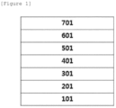
- FIG. 1 illustrates an example of an organic light emitting device according to an exemplary embodiment of the present specification.
- the present specification provides a polymer including: the first unit represented by Formula 103; and the second unit represented by Formula 2.
- the first unit represented by Formula 103 and the second unit represented by Formula 2 may constitute a random polymer.
- the "unit” means a structure in which a monomer is included and repeated in a polymer, and a structure in which the monomer is bonded into the polymer by polymerization.
- the "monomer” means a monomer or a unit body which is a unit constituting the polymer.
- the first unit represented by Formula 103 has excellent solubility to an organic solvent. Accordingly, when the polymer including the first unit represented by Formula 103 is used in a hole transport layer or a hole injection layer in an organic light emitting device, a solution process is easily applied and uniformity, surface characteristics, and the like of a hole transport layer or hole injection layer manufactured are also excellent, so that it is possible to improve performance and service life characteristics of the device.
- the second unit represented by Formula 2 is derived from a compound having a curing group and a vinyl group.
- a polymer which does not include an additional curing group has a disadvantage in that the polymer cannot exhibit sufficient solvent resistance.
- the second unit represented by Formula 2 according to the present specification may form a cross-linking bond through a heat treatment due to an additional curing group, and has an effect of exhibiting sufficient solvent resistance.
- the "curing group” may mean a reactive substituent which cross-links compounds by being exposed to heat and/or light.
- the cross-linkage may be produced while radicals produced by decomposing carbon-carbon multiple bond and cyclic structures by means of a heat treatment or light irradiation are linked to each other.
- substitution means that a hydrogen atom bonded to a carbon atom of a compound is changed into another substituent, and a position to be substituted is not limited as long as the position is a position at which the hydrogen atom is substituted, that is, a position at which the substituent may be substituted, and when two or more are substituted, the two or more substituents may be the same as or different from each other.
- an alkoxy group may be straight-chained, branched, or cyclic.
- the number of carbon atoms of the alkoxy group is not particularly limited, but is preferably 1 to 20. Specific examples thereof include methoxy, ethoxy, n-propoxy, isopropoxy, i-propyloxy, n-butoxy, isobutoxy, tert-butoxy, sec-butoxy, n-pentyloxy, neopentyloxy, isopentyloxy, n-hexyloxy, 3,3-dimethylbutyloxy, 2-ethylbutyloxy, n-octyloxy, n-nonyloxy, n-decyloxy, benzyloxy, p-methylbenzyloxy, and the like, but are not limited thereto.
- examples of an aryloxy group include a phenoxy group, a p-tolyloxy group, an m-tolyloxy group, a 3,5-dimethyl-phenoxy group, a 2,4,6-trimethylphenoxy group, a p-tert-butylphenoxy group, a 3-biphenyloxy group, a 4-biphenyloxy group, a 1-naphthyloxy group, a 2-naphthyloxy group, a 4-methyl-1-naphthyloxy group, a 5-methyl-2-naphthyloxy group, a 1-anthracenyloxy group, a 2-anthracenyloxy group, a 9-anthracenyloxy group, a 1-phenanthryloxy group, a 3-phenanthryloxy group, a 9-phenanthryloxy group, and the like, but are not limited thereto.
- a cycloalkyl group is not particularly limited, but has preferably 3 to 60 carbon atoms, and more preferably 3 to 30 carbon atoms.
- Specific examples thereof include cyclopropyl, cyclobutyl, cyclopentyl, 3-methylcyclopentyl, 2,3-dimethylcyclopentyl, cyclohexyl, 3-methylcyclohexyl, 4-methylcyclohexyl, 2,3-dimethylcyclohexyl, 3,4,5-trimethylcyclohexyl, 4-tert-butylcyclohexyl, cycloheptyl, cyclooctyl, and the like, but are not limited thereto.
- an aryl group is a monocyclic aryl group
- the number of carbon atoms thereof is not particularly limited, but is preferably 6 to 50, and more preferably 6 to 30.
- Specific examples of the monocyclic aryl group include a phenyl group, a biphenyl group, a terphenyl group, a quarterphenyl group, and the like, but are not limited thereto.
- the aryl group is a polycyclic aryl group
- the number of carbon atoms thereof is not particularly limited, but is preferably 10 to 50, and more preferably 10 to 30.
- Specific examples of the polycyclic aryl group include a naphthyl group, an anthracenyl group, a phenanthryl group, a pyrenyl group, a perylenyl group, a triphenyl group, a chrysenyl group, a fluorenyl group, and the like, but are not limited thereto.
- the fluorenyl group may be substituted, and adjacent substituents may be bonded to each other to form a ring.
- the substituent may be , and the like, but is not limited thereto.
- a heterocyclic group includes one or more of N, O, S, Si, and Se as a heteroatom, and the number of carbon atoms thereof is not particularly limited, but is preferably 2 to 60, and more preferably 2 to 30.
- the heterocyclic group include a thiophene group, a furan group, a pyrrole group, an imidazole group, a thiazole group, an oxazole group, an oxadiazole group, a triazole group, a pyridine group, a bipyridine group, a pyrimidine group, a triazine group, an acridine group, a pyridazine group, a pyrazine group, a quinoline group, a quinazoline group, a quinoxaline group, a phthalazine group, a pteridine group, a pyrido pyrimidine group, a pyrido pyrazine
- a heteroaryl group may be selected from the examples of the heterocyclic group except for an aromatic heteroaryl group, but is not limited thereto.
- an alkylene group means a group having two bonding positions in an alkyl group, that is, a divalent group.
- the above-described description on the alkyl group may be applied to the alkylene group, except for a divalent alkylene group.
- an arylene group means a group having two bonding positions in an aryl group, that is, a divalent group.
- the above-described description on the aryl group may be applied to the arylene group, except for a divalent arylene group.
- a heteroarylene group means a group having two bonding positions in a heteroaryl group, that is, a divalent group.
- the above-described description on the heteroaryl group may be applied to the heteroarylene group, except for a divalent heteroarylene group.
- L2 to L6 are the same as or different from each other, and are each independently a direct bond; -O-; a substituted or unsubstituted alkylene group; a substituted or unsubstituted arylene group; a substituted or unsubstituted divalent amine group; or a substituted or unsubstituted heteroarylene group.
- L2 to L6 are the same as or different from each other, and are each independently a substituted or unsubstituted arylene group having 6 to 30 carbon atoms.
- L2 to L6 are the same as or different from each other, and are each independently a substituted or unsubstituted phenylene group; a substituted or unsubstituted biphenylene group; a substituted or unsubstituted naphthylene group; or a substituted or unsubstituted fluorenylene group.
- L2 is a direct bond.
- L2 is a substituted or unsubstituted arylene group having 6 to 30 carbon atoms.
- L2 is a phenylene group or a biphenylene group.
- L3 and L4 are the same as or different from each other, and are each independently a substituted or unsubstituted arylene group having 6 to 30 carbon atoms.
- L3 and L4 are the same as or different from each other, and are each independently a substituted or unsubstituted phenylene group, a substituted or unsubstituted biphenylene group, a substituted or unsubstituted naphthylene group, or a substituted or unsubstituted fluorenylene group.
- L3 is a direct bond.
- L3 is a phenylene group.
- L4 is a phenylene group.
- L5 is a direct bond.
- L5 is a substituted or unsubstituted arylene group having 6 to 30 carbon atoms.
- L5 is a phenylene group.
- L6 is a direct bond.
- L6 is a divalent amine group which is unsubstituted or substituted with a phenyl group.
- L6 is a substituted or unsubstituted alkylene group having 1 to 20 carbon atoms.
- L6 is a substituted or unsubstituted alkylene group having 1 to 10 carbon atoms.
- L6 is a methylene group, an ethylene group, a propylene group, a butylene group, a pentylene group, or a hexylene group.
- L6 is a methylene group.
- (L6)b2 is a direct bond; a methylene group; an ethylene group; a phenylene-O-hexylene group; a phenylene-methylene group; a divalent amine group substituted with a phenylene-phenyl group; a divalent amine group substituted with a phenyl group; a phenylene group; or a biphenylene group.
- the phenylene-methylene group is a group in which a phenylene group and a methylene group are linked.
- the phenylene-O-hexylene group is a group in which a phenylene group, -O-, and a hexylene group are consecutively linked.
- the divalent amine group substituted with the phenylene-phenyl group is a group in which a divalent amine group substituted with the phenylene group and the phenyl group is linked.
- b2 is an integer from 1 to 10, and when b2 is 2 or more, two or more L6's are each the same as or different from each other.
- b2 is an integer from 1 to 5.
- b2 is an integer from 1 to 3.
- Ar1 to Ar3 are the same as or different from each other, and are each independently a substituted or unsubstituted alkyl group; a substituted or unsubstituted alkoxy group; a substituted or unsubstituted aryloxy group; a substituted or unsubstituted aryl group; or a substituted or unsubstituted heterocyclic group.
- Ar1 is an aryl group having 6 to 30 carbon atoms which is unsubstituted or substituted with one or more substituents selected from the group consisting of an alkyl group; an alkoxy group; an aryloxy group; an aryl group; and a heterocyclic group, or a substituent formed by linking two or more substituents selected from the above group.
- Ar1 is an aryl group having 6 to 30 carbon atoms which is unsubstituted or substituted with one or more substituents selected from the group consisting of an alkyl group having 1 to 10 carbon atoms; an alkoxy group having 1 to 10 carbon atoms; an aryloxy group having 6 to 30 carbon atoms; an aryl group having 6 to 30 carbon atoms; and a heterocyclic group having 2 to 30 carbon atoms or a substituent formed by linking two or more substituents selected from the above group.
- Ar1 is a substituted or unsubstituted alkyl group having 1 to 30 carbon atoms.
- Ar1 is a methyl group, an ethyl group, an isopropyl group, or a tert-butyl group.
- Ar1 is a substituted or unsubstituted alkoxy group having 1 to 20 carbon atoms.
- Ar1 is a methoxy group.
- Ar1 is an isopropoxy group.
- Ar1 is a tert-butoxy group.
- Ar1 is a substituted or unsubstituted aryl group having 6 to 30 carbon atoms.
- Ar1 is a phenyl group.
- Ar2 and Ar3 are the same as or different from each other, and are each independently a substituted or unsubstituted phenyl group, a substituted or unsubstituted biphenyl group, a substituted or unsubstituted terphenyl group, a substituted or unsubstituted naphthyl group, a substituted or unsubstituted phenanthryl group, or a substituted or unsubstituted fluorenyl group.
- Ar2 is a fluorenyl group which is substituted with an alkyl group.
- Ar2 is a fluorenyl group which is substituted with a methyl group.
- Ar3 is a fluorenyl group which is substituted with an alkyl group.
- R1 to R8 are the same as or different from each other, and are each independently hydrogen; deuterium; a halogen group; a hydroxyl group; a nitrile group; a substituted or unsubstituted alkyl group; a substituted or unsubstituted cycloalkyl group; a substituted or unsubstituted aryl group; or a substituted or unsubstituted heterocyclic group.
- R1 to R8 are each hydrogen.
- r4 and r5 are each an integer from 1 to 3, and when r4 and r5 are each 2 or more, two or more R4's and R5's are each the same as or different from each other.
- m1 is a mole fraction and 0 ⁇ m1 ⁇
- m2 is a mole fraction and 0 ⁇ m2 ⁇ 1
- m1 is 0.01 ⁇ m1 ⁇ 0.99
- m2 is 0.01 ⁇ m2 ⁇ 0.59.
- m1 is 0.5 ⁇ m1 ⁇ 0.99
- m2 is 0.01 ⁇ m2 ⁇ 0.5.
- m1 > m2.
- m1 + m2 is 1.
- X is any one selected from the following structures.
- the structures are any one selected from the following structures.
- X is selected from the following structures.
- X is
- X is cyclobutabenzene or oxetane.
- X is cyclobutabenzene or oxetane
- AIBN a radical initiation reaction using azobisisobutyronitrile
- curing begins, and as a result, a cross-linked polymer may be formed, and the polymer exhibits high resistance, and thus is easy to be used for the solution process.
- L11 is a methylene group; an ethylene group; a propylene group; a butylene group; a phenylene group, or a biphenylene group.
- R10 to R13 are the same as or different from each other, and are each independently hydrogen; a methyl group; an ethyl group; a propyl group; an isopropyl group; a butyl group; or a t-butyl group.
- L101 of Formula 103 is a direct bond.
- Formula 2 is represented by the following Formula 201 or 202.
- Formulae 201 and 202 are represented by the following Formula 201 or 202.
- L106 of Formulae 201 and 202 is the same as the definition of L6 of Formula 2.
- b102 of Formulae 201 and 202 is 1 or 2.
- L106 of Formulae 201 and 202 is a direct bond.
- R20 and R21 of Formulae 201 and 202 are the same as or different from each other, and are each independently hydrogen; deuterium; or an alkyl group.
- R20 and R21 of Formulae 201 and 202 are the same as or different from each other, and are each independently hydrogen; deuterium; or a methyl group.
- the first unit represented by Formula 103 may be represented by any one of the following structures.
- m1 is a mole fraction and 0 ⁇ m1 ⁇ 1.
- the second unit represented by Formula 2 may be represented by any one of the following structures.
- m2 is a mole fraction and 0 ⁇ m2 ⁇ 1.
- a polymer including the first unit represented by Formula 103 and the second unit represented by Formula 2 may be represented by the following Formula 11 or 12.
- Formulae 11 and 12
- the polymer including the first unit represented by Formula 103 and the second unit represented by Formula 2 may be any one selected from the following structures.
- the structures In the structures,
- the polymer including the first unit represented by Formula 103 and the second unit represented by Formula 2 may be any one selected from the following structures.
- the polymer may have a number average molecular weight of 5,000 g/mol to 1,000,000 g/mol. Specifically, the polymer may have a number average molecular weight of 5,000 g/mol to 300,000 g/mol.
- the polymer according to an exemplary embodiment of the present specification may be prepared by a preparation method described below. Representative examples will be described in the Preparation Examples described below, but if necessary, a substituent may be added or excluded, and the position of the substituent may be changed. Further, a starting material, a reactant, reaction conditions, and the like may be changed based on the technology known in the art.
- the polymer including the first unit represented by Formula 103 and the second unit represented by Formula 2 may be prepared as in the following Reaction Formula 1.
- definitions of X, L101, L2 to L6, b101, b2, Ar1 to Ar3, R1 to R8, r4, r5, m1, and m2 are the same as those defined in Formulae 103 and 2.
- azobisisobutyronitrile (AIBN) is used during the preparation of the coating composition.
- the coating composition may further include a solvent.
- the coating composition may be in a liquid phase.
- the "liquid phase” means that the composition is in a liquid state at room temperature under atmospheric pressure.
- the solvents may be used either alone or in a mixture of two or more solvents.
- a boiling point of the solvent is preferably 40°C to 250°C, and more preferably 60°C to 230°C, but is not limited thereto.
- a concentration of the coating composition is preferably 0.1 wt/v% to 20 wt/v%, and more preferably 0.5 wt/v% to 5 wt/v%, but is not limited thereto.
- the coating composition may further include one or two or more additives selected from the group consisting of a thermal polymerization initiator and a photopolymerization initiator.
- compounds having photopolymerization promoting effects may be used either alone or in combination with the photopolymerization initiators.
- examples thereof include triethanolamine, methyldiethanolamine, ethyl 4-dimethylaminobenzoate, isoamyl 4-dimethylaminobenzoate, (2-dimethylamino)ethyl benzoate, 4,4'-dimethylamino benzophenone, and the like, but are not limited thereto.
- the present specification also provides an organic light emitting device formed by using the coating composition.
- the first electrode is an anode
- the second electrode is a cathode
- the cured product of the coating composition is in a state in which the coating composition is cured by a heat treatment or a light treatment.
- the organic material layer including the cured product of the coating composition is a hole transport layer, a hole injection layer, or a layer which simultaneously transports and injects holes.
- the organic material layer including the cured product of the coating composition includes a light emitting layer, and the light emitting layer includes the cured product of the coating composition.
- the coating composition may further include a p-doping material (p-dopant).
- the p-doping material includes F 4 TCNQ; or a boron anion, and the boron anion includes a halogen group.
- the p-doping material includes F 4 TCNQ; or a boron anion, and the boron anion includes F.
- the p-doping material is selected from the following structural formulae.
- a content of the p-doping material is 0.001 wt% to 50 wt%; 0.01 wt% to 30 wt%; or 1 wt% to 25 wt%, based on the total weight 100% of the coating composition.
- the organic light emitting device may further include one or two or more layers selected from the group consisting of a hole injection layer, a hole transport layer, an electron transport layer, an electron injection layer, an electron blocking layer, and a hole blocking layer.
- the organic light emitting device may be an organic light emitting device having an inverted type structure in which a cathode, an organic material layer having one or more layer, and an anode are sequentially stacked on a substrate.
- the organic material layer of the organic light emitting device of the present specification may also be composed of a single-layered structure, but may be composed of a multi-layered structure in which an organic material layer having two or more layers is stacked.
- the organic light emitting device of the present specification may have a structure including a hole injection layer, a hole transport layer, a light emitting layer, an electron transport layer, an electron injection layer, and the like as organic material layers.
- the structure of the organic light emitting device is not limited thereto, and may include a fewer number of organic material layers.
- FIG. 1 the structure of the organic light emitting device according to an exemplary embodiment of the present specification is exemplified in FIG. 1 .
- FIG. 1 exemplifies a structure of an organic light emitting device in which an anode 201, a hole injection layer 301, a hole transport layer 401, a light emitting layer 501, a layer 601 which simultaneously injects and transports electrons, and a cathode 701 are sequentially stacked on a substrate 101.
- the hole injection layer 301, the hole transport layer 401, or the light emitting layer 501 in FIG. 1 may be formed by using a coating composition including a polymer including: the first unit represented by Formula 103; and a second unit represented by the following Formula 2.
- the hole injection layer 301 in FIG. 1 may be formed by using a coating composition including a polymer including: the first unit represented by Formula 103; and a second unit represented by the following Formula 2.
- FIG. 1 exemplifies an organic light emitting device, and the organic light emitting device is not limited thereto.
- the organic material layers may be formed of the same material or different materials.
- the organic light emitting device of the present specification may be manufactured by sequentially stacking an anode, an organic material layer, and a cathode on a substrate.
- the organic light emitting device may be manufactured by depositing a metal or a metal oxide having conductivity, or an alloy thereof on a substrate to form an anode, forming an organic material layer including a hole injection layer, a hole transport layer, a light emitting layer, and an electron transport layer thereon, and then depositing a material, which may be used as a cathode, thereon, by using a physical vapor deposition (PVD) method such as sputtering or e-beam evaporation.
- PVD physical vapor deposition
- an organic light emitting device may be manufactured by sequentially depositing a cathode material, an organic material layer, and an anode material on a substrate.
- the present specification also provides a method for manufacturing an organic light emitting device formed by using the coating composition.
- an exemplary embodiment of the present specification provides a method for manufacturing an organic light emitting device, the method including: preparing a substrate; forming a cathode or an anode on the substrate; forming an organic material layer having one or more layers on the cathode or the anode; and forming an anode or a cathode on the organic material layer, in which the forming of the organic material layer includes forming an organic material layer having one or more layers by using the coating composition.
- the organic material layer formed by using the coating composition is formed by a printing method.
- examples of the printing method include inkjet printing, nozzle printing, offset printing, transfer printing or screen printing, and the like, but are not limited thereto.
- the coating composition according to an exemplary embodiment of the present specification is suitable for a solution process due to the structural characteristics thereof, so that the organic material layer may be formed by a printing method, and as a result, there is an economic effect in terms of time and costs when a device is manufactured.
- the forming of the organic material layer formed by using the coating composition includes: coating the cathode or the anode with the coating composition; and subjecting the coating composition to a heat treatment or a light treatment.
- the time for subjecting the organic material layer formed by using the coating composition to a heat treatment is preferably within 1 hour, and more preferably within 30 minutes.
- an atmosphere under which the organic material layer formed by using the coating composition is subjected to a heat treatment is preferably an inert gas such as argon and nitrogen.
- the coating composition including the polymer may use a coating composition dispersed by being mixed with a polymer binding agent.
- polymer binding agent those which do not extremely suppress charge transport are preferred, and those which are not strong in absorption to visible light are preferably used.
- polymeric binding agent poly(N-vinylcarbazole), polyaniline, and derivatives thereof, polythiophene and derivatives thereof, poly(p-phenylene vinylene) and derivatives thereof, poly(2,5-thienylene vinylene) and derivatives thereof, polycarbonate, polyacrylate, polymethyl acrylate, polymethyl methacrylate, polystyrene, polyvinyl chloride, polysiloxane, and the like are exemplified.
- the polymer according to an exemplary embodiment of the present specification may also be included as a compound alone, and may be included as a copolymer by using a coating composition mixed with another monomer, in an organic material layer.
- the polymer may be included as a copolymer or a mixture by using a coating composition mixed with another polymer.
- anode material materials having a high work function are usually preferred so as to facilitate the injection of holes into an organic material layer.
- anode material which may be used in the present specification include: a metal, such as vanadium, chromium, copper, zinc, and gold, or an alloy thereof; a metal oxide, such as zinc oxide, indium oxide, indium tin oxide (ITO), and indium zinc oxide (IZO); a combination of metal and oxide, such as ZnO : Al or SnO 2 : Sb; a conductive polymer, such as poly(3-methylthiophene), poly[3,4-(ethylene-1,2-dioxy)thiophene] (PEDOT), polypyrrole, and polyaniline; and the like, but are not limited thereto.
- a metal such as vanadium, chromium, copper, zinc, and gold, or an alloy thereof
- a metal oxide such as zinc oxide, indium oxide, indium tin oxide (ITO), and indium zinc oxide (IZO)
- the hole injection layer is a layer which injects holes from an electrode
- a hole injection material is preferably a compound which has a capability of transporting holes and thus has an effect of injecting holes at an anode and an excellent effect of injecting holes into a light emitting layer or a light emitting material, prevents excitons produced from the light emitting layer from moving to an electron injection layer or an electron injection material, and is also excellent in the ability to form a thin film.
- the highest occupied molecular orbital (HOMO) of the hole injection material is preferably a value between the work function of the anode material and the HOMO of the neighboring organic material layer.
- the hole injection material examples include metal porphyrin, oligothiophene, an arylamine-based organic material, a hexanitrile hexaazatriphenylene-based organic material, a quinacridone-based organic material, a perylene-based organic material, anthraquinone, polyaniline-based and polythiophene-based conductive polymers, and the like, but are not limited thereto.
- the hole transport layer is a layer which accepts holes from a hole injection layer and transports the holes to a light emitting layer
- the hole transport material is suitably a material having high hole mobility which may accept holes from an anode or a hole injection layer to transfer the holes to a light emitting layer.
- Specific examples thereof include an arylamine-based organic material, a conductive polymer, a block copolymer having both conjugated portions and non-conjugated portions, and the like, but are not limited thereto.
- the light emitting material is a material which may emit light in a visible light region by accepting and combining holes and electrons from a hole transport layer and an electron transport layer, respectively, and preferably a material having high quantum efficiency for fluorescence or phosphorescence.
- Specific examples thereof include: an 8-hydroxy-quinoline aluminum complex (Alq 3 ); a carbazole-based compound; a dimerized styryl compound; BAlq; a 10-hydroxybenzoquinoline-metal compound; benzoxazole-based, benzothiazole-based and benzimidazole-based compounds; a poly(p-phenylenevinylene) (PPV)-based polymer; a spiro compound; polyfluorene; lubrene, and the like, but are not limited thereto.
- PV poly(p-phenylenevinylene)
- the light emitting layer may include a host material and a dopant material.
- the host material include fused aromatic ring derivatives, or hetero ring-containing compounds, and the like.
- the fused aromatic ring derivative include an anthracene derivative, a pyrene derivative, a naphthalene derivative, a pentacene derivative, a phenanthrene compound, a fluoranthene compound, and the like
- examples of the hetero ring-containing compound include a carbazole derivative, a dibenzofuran derivative, a ladder-type furan compound, a pyrimidine derivative, and the like, but the examples thereof are not limited thereto.
- the dopant material examples include an aromatic amine derivative, a styrylamine compound, a boron complex, a fluoranthene compound, a metal complex, and the like.
- the aromatic amine derivative is a fused aromatic ring derivative having a substituted or unsubstituted arylamine group, and examples thereof include a pyrene, an anthracene, a chrysene, a periflanthene, and the like, which have an arylamine group
- the styrylamine compound is a compound in which a substituted or unsubstituted arylamine is substituted with at least one arylvinyl group, and one or two or more substituents selected from the group consisting of an aryl group, a silyl group, an alkyl group, a cycloalkyl group, and an arylamine group are substituted or unsubstituted.
- examples thereof include styrylamine, styryldiamine, styryltriamine, styryltetramine, and the like, but are not limited thereto.
- examples of the metal complex include an iridium complex, a platinum complex, and the like, but are not limited thereto.
- the electron transport layer is a layer which accepts electrons from an electron injection layer and transports the electrons to a light emitting layer
- an electron transport material is suitably a material having high electron mobility which may proficiently accept electrons from a cathode and transfer the electrons to a light emitting layer.
- Specific examples thereof include: an Al complex of 8-hydroxyquinoline; a complex including Alq 3 ; an organic radical compound; a hydroxyflavone-metal complex; and the like, but are not limited thereto.
- the electron transport layer may be used with any desired cathode material, as used according to the related art.
- appropriate examples of the cathode material are a typical material which has a low work function, followed by an aluminum layer or a silver layer.
- Specific examples thereof include cesium, barium, calcium, ytterbium, and samarium, in each case followed by an aluminum layer or a silver layer.
- fluorenone anthraquinodimethane, diphenoquinone, thiopyran dioxide, oxazole, oxadiazole, triazole, imidazole, perylenetetracarboxylic acid, fluorenylidene methane, anthrone, and the like, and derivatives thereof, metal complex compounds, nitrogen-containing 5-membered ring derivatives, and the like, but are not limited thereto.
- Examples of the metal complex compounds include 8-hydroxyquinolinato lithium, bis(8-hydroxyquinolinato) zinc, bis(8-hydroxyquinolinato) copper, bis(8-hydroxyquinolinato) manganese, tris(8-hydroxyquinolinato) aluminum, tris(2-methyl-8-hydroxyquinolinato) aluminum, tris(8-hydroxyquinolinato) gallium, bis(10-hydroxybenzo[h]quinolinato) beryllium, bis(10-hydroxybenzo[h]quinolinato) zinc, bis(2-methyl-8-quinolinato) chlorogallium, bis(2-methyl-8-quinolinato)(o-cresolato) gallium, bis(2-methyl-8-quinolinato)(1-naphtholato) aluminum, bis(2-methyl-8-quinolinato)(2-naphtholato) gallium, and the like, but are not limited thereto.
- the organic light emitting device may be a top emission type, a bottom emission type, or a dual emission type according to the materials to be used.
- the compound may be included in an organic solar cell or an organic transistor in addition to the organic light emitting device.
- Compound A2 was prepared in the same manner as in the method of preparing Compound A1, except that 4-(dibiphenyl-4-yl amino)phenyl boronic acid was used instead of 4-(diphenylamino)phenyl boronic acid.
- Compound A3 was prepared in the same manner as in the method of preparing Compound A1, except that 4-(biphenyl-4-yl(9,9-dimethyl-9H-fluoren-2-yl)amino)phenyl boronic acid was used instead of 4-(diphenylamino)phenyl boronic acid.
- Polymer C2 was prepared in the same manner as in the method of preparing Polymer C1, except that Compound A3 and 4-vinyl-1,2-dihydrobutabenzene were used instead of Compound A1 and Compound B2.
- Mn 25,700
- Mw 47,900
- Polymer C3 was prepared in the same manner as in the method of preparing Polymer C1, except that Compound A6 and 4-vinyl-1,2-dihydrobutabenzene were used instead of Compound A1 and Compound B2.
- Polymer C4 was prepared in the same manner as in the method of preparing Polymer C1, except that Compound A9 was used instead of Compound A1.
- a glass substrate thinly coated with indium tin oxide (ITO) to have a thickness of 1,500 ⁇ was put into distilled water in which a detergent was dissolved, and ultrasonically washed.
- ITO indium tin oxide
- a product manufactured by Fischer Co. was used as the detergent
- distilled water, which had been filtered twice with a filter manufactured by Millipore Co. was used as the distilled water.
- ultrasonic washing was conducted twice repeatedly using distilled water for 10 minutes.
- the ITO surface of a transparent ITO electrode was spin-coated (4,000 rpm) with 2 wt% of a toluene ink of Polymer C1 : the following p-dopant (the following Formula M) (weight ratio of 8 : 2) and the transparent ITO electrode was heat-treated (cured) at 200°C for 30 minutes, thereby forming a hole injection layer having a thickness of 40 nm. Thereafter, the transparent ITO electrode was transported to a vacuum deposition machine, and then a hole transport layer was formed to have a thickness of 20 nm by vacuum-depositing the following Compound G onto the hole injection layer.
- Compound H and Compound I were vacuum-deposited to have a thickness of 20 nm on the hole transport layer, thereby forming a light emitting layer.
- Compound J was vacuum-deposited to have a thickness of 35 nm on the light emitting layer, thereby forming a layer which simultaneously injects and transports electrons.
- LiF and aluminum were sequentially deposited on the layer, which simultaneously injects and transports electrons, to have a thickness of 1 nm and 100 nm, respectively, thereby forming a cathode.
- the deposition rate of the organic material was maintained at 0.4 to 0.7 ⁇ /sec
- the deposition rates of lithium fluoride and aluminum of the cathode were maintained at 0.3 ⁇ /sec and at 2 ⁇ /sec, respectively
- the degree of vacuum during the deposition was maintained at 2 ⁇ 10 -7 to 5 ⁇ 10 -8 torr, thereby manufacturing an organic light emitting device.
- An organic light emitting device was manufactured in the same manner as in the procedure in Device Example 1, except that 2 wt% of a toluene ink of Polymer C3 : the p-dopant (weight ratio of 8 : 2) was used instead of 2 wt% of the toluene ink of Polymer C1 : the p-dopant (weight ratio of 8 : 2) during the film-formation of the hole injection layer in the manufacturing procedure in Device Example 1.
- An organic light emitting device was manufactured in the same manner as in the procedure in Device Example 1, except that 2 wt% of a toluene ink of the following Polymer F : the p-dopant (weight ratio of 8 : 2) was used instead of 2 wt% of the toluene ink of Polymer C1 : the p-dopant (weight ratio of 8 : 2) during the film-formation of the hole injection layer in the manufacturing procedure in Device Example 1.
- An organic light emitting device was manufactured in the same manner as in the procedure in Device Example 1, except that 2 wt% of a toluene ink of the following Polymer Z : the p-dopant (weight ratio of 8 : 2) was used instead of 2 wt% of the toluene ink of Polymer C1 : the p-dopant (weight ratio of 8 : 2) during the film-formation of the hole injection layer in the manufacturing procedure in Device Example 1.
- the coating composition using the polymer including the first unit represented by Formula 103 and the second unit represented by Formula 2 according to the present specification is excellent in uniformity of the coating layer and stability of the film, it is possible to improve the performance of the organic light emitting device by using the coating composition.
Landscapes
- Chemical & Material Sciences (AREA)
- Organic Chemistry (AREA)
- Materials Engineering (AREA)
- Engineering & Computer Science (AREA)
- Chemical Kinetics & Catalysis (AREA)
- Medicinal Chemistry (AREA)
- Polymers & Plastics (AREA)
- Health & Medical Sciences (AREA)
- Life Sciences & Earth Sciences (AREA)
- Wood Science & Technology (AREA)
- Physics & Mathematics (AREA)
- Optics & Photonics (AREA)
- Electroluminescent Light Sources (AREA)
- Compositions Of Macromolecular Compounds (AREA)
- Addition Polymer Or Copolymer, Post-Treatments, Or Chemical Modifications (AREA)
Claims (14)
- Polymer, umfassend:eine durch die folgende Formel 103 dargestellte erste Einheit undeine durch die folgende Formel 2 dargestellte zweite Einheit:

 sind L2 bis L6 gleich oder verschieden voneinander und sind jeweils unabhängig eine direkte Bindung, -O-, eine substituierte oder unsubstituierte Alkylengruppe, eine substituierte oder unsubstituierte Arylengruppe, eine substituierte oder unsubstituierte zweiwertige Amingruppe oder eine substituierte oder unsubstituierte Heteroarylengruppe,b2 ist eine ganze Zahl von 1 bis 10,wenn b2 2 oder größer ist, sind zwei oder mehr L6 jeweils gleich oder verschieden voneinander,Ar1 bis Ar3 sind gleich oder verschieden voneinander und sind jeweils unabhängig eine substituierte oder unsubstituierte Alkylgruppe, eine substituierte oder unsubstituierte Alkoxygruppe, eine substituierte oder unsubstituierte Aryloxygruppe, eine substituierte oder unsubstituierte Arylgruppe oder eine substituierte oder unsubstituierte heterocyclische Gruppe,R1 bis R8 sind gleich oder verschieden voneinander und sind jeweils Wasserstoff, Deuterium, eine Halogengruppe,eine Hydroxylgruppe, eine Nitrilgruppe, eine substituierte oder unsubstituierte Alkylgruppe, eine substituierte oder unsubstituierte Cycloalkylgruppe, eine substituierte oder unsubstituierte Arylgruppe oder eine substituierte oder unsubstituierte heterocyclische Gruppe,r4 und r5 sind jeweils eine ganze Zahl von 1 bis 3,wenn r4 und r5 jeweils zwei oder größer sind, sind zwei oder mehr R4 und R5 jeweils gleich oder verschieden voneinander,m1 ist ein Molanteil und 0 < m1 < 1,m2 ist ein Molanteil und 0 < m2 < 1,m1 + m2 ≤ 1,X ist eines, ausgewählt aus den folgenden Strukturen,


 ist L11 eine substituierte oder unsubstituierte Alkylengruppe oder eine substituierte oder unsubstituierte Arylengruppe,R10 bis R13 sind gleich oder verschieden voneinander und jeweils unabhängig Wasserstoff oder eine substituierte oder unsubstituierte Alkylgruppe mit 1 bis 6 Kohlenstoffatomenwenn X
 L101 ist eine direkte Bindung, -O-, eine substituierte oder unsubstituierte Alkylengruppe, eine substituierte oder unsubstituierte Arylengruppe, eine substituierte oder unsubstituierte zweiwertige Amingruppe oder eine substituierte oder unsubstituierte Heteroarylengruppe,b101 ist eine ganze Zahl von 1 bis 9 undwenn b101 2 oder größer ist, sind zwei oder mehr L101 jeweils gleich oder verschieden voneinander.
 - Polymer gemäß Anspruch 1, worin Ar1 eine Arylgruppe mit 6 bis 30 Kohlenstoffatomen ist, die unsubstituiert oder mit einem oder mehreren Substituenten, ausgewählt aus der Gruppe, bestehend aus einer Alkylgruppe, einer Alkoxygruppe, einer Aryloxygruppe, einer Arylgruppe und einer heterocyclischen Gruppe, oder einem Substituenten, der durch Verknüpfen von zwei oder mehr Substituenten, ausgewählt aus der obigen Gruppe, gebildet wird, substituiert ist.
- Polymer gemäß Anspruch 1, worin Ar2 und Ar3 gleich oder verschieden voneinander sind und jeweils unabhängig eine substituierte oder unsubstituierte Phenylgruppe, eine substituierte oder unsubstituierte Biphenylgruppe, eine substituierte oder unsubstituierte Terphenylgruppe, eine substituierte oder unsubstituierte Naphthylgruppe, eine substituierte oder unsubstituierte Phenanthrylgruppe oder eine substituierte oder unsubstituierte Fluorenylgruppe sind.
- Polymer gemäß Anspruch 1, worin R1 bis R8 jeweils Wasserstoff sind.
- Polymer gemäß Anspruch 1, worin die durch Formel 103 dargestellte erste Einheit durch eine der folgenden Strukturen dargestellt ist:


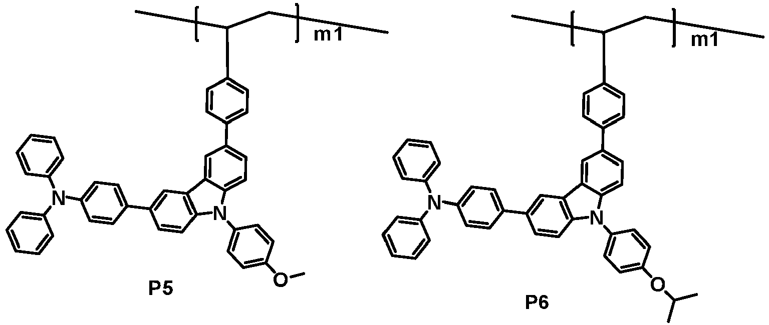


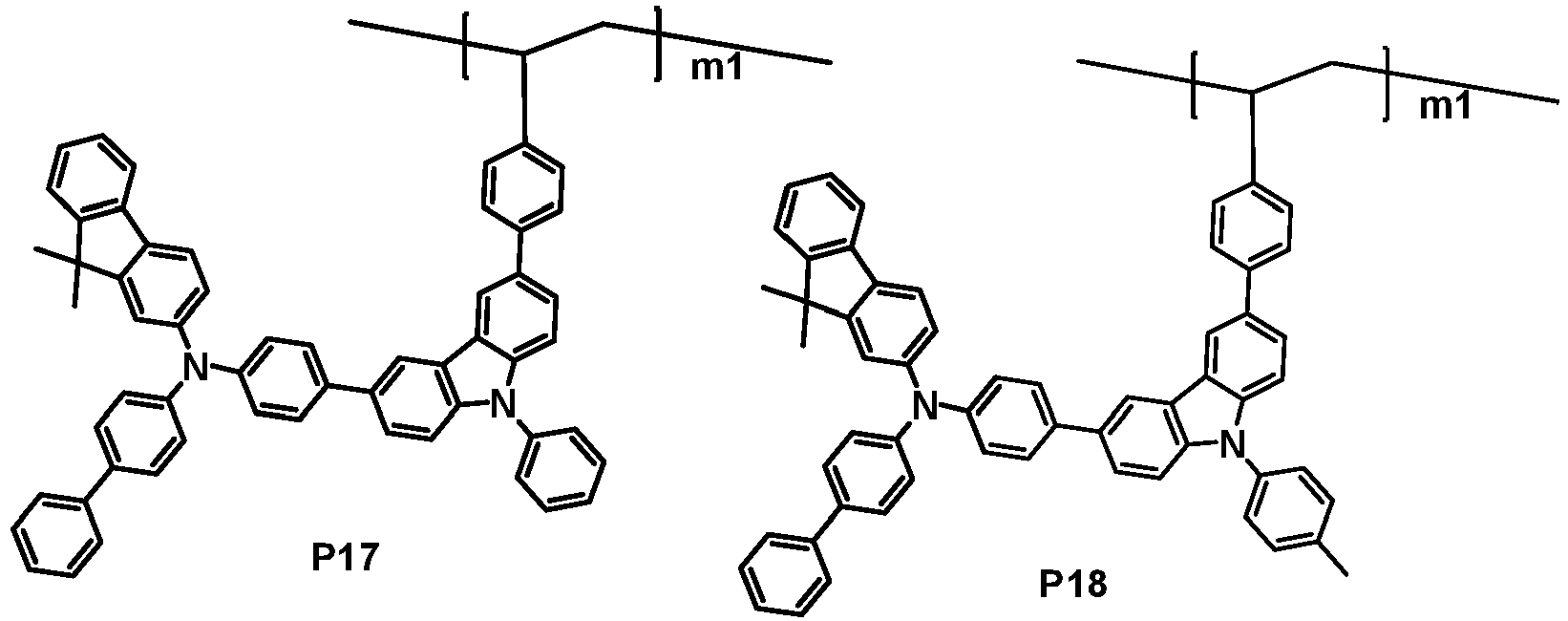
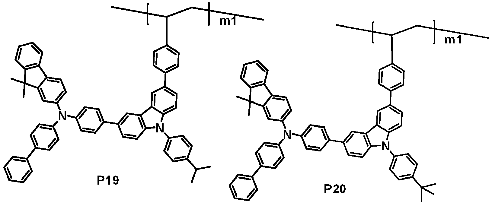


ist m1 ein Molanteil und 0 < m1 < 1. - Polymer gemäß Anspruch 1, worin die durch Formel 2 dargestellte zweite Einheit durch eine der folgenden Strukturen dargestellt ist:
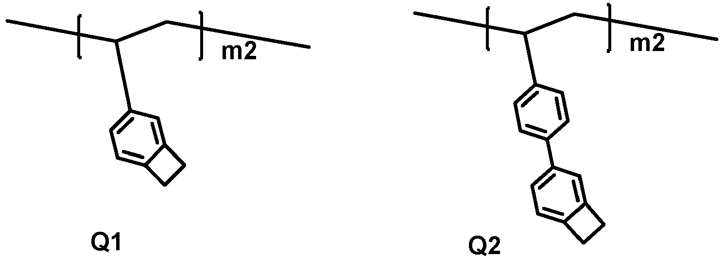


ist m2 ein Molanteil und 0 < m2 < 1. - Polymer gemäß Anspruch 1, wobei das Polymer, das die durch Formel 103 dargestellte erste Einheit und die durch Formel 2 dargestellte zweite Einheit umfasst, eines, ausgewählt aus den folgenden Strukturen, ist:


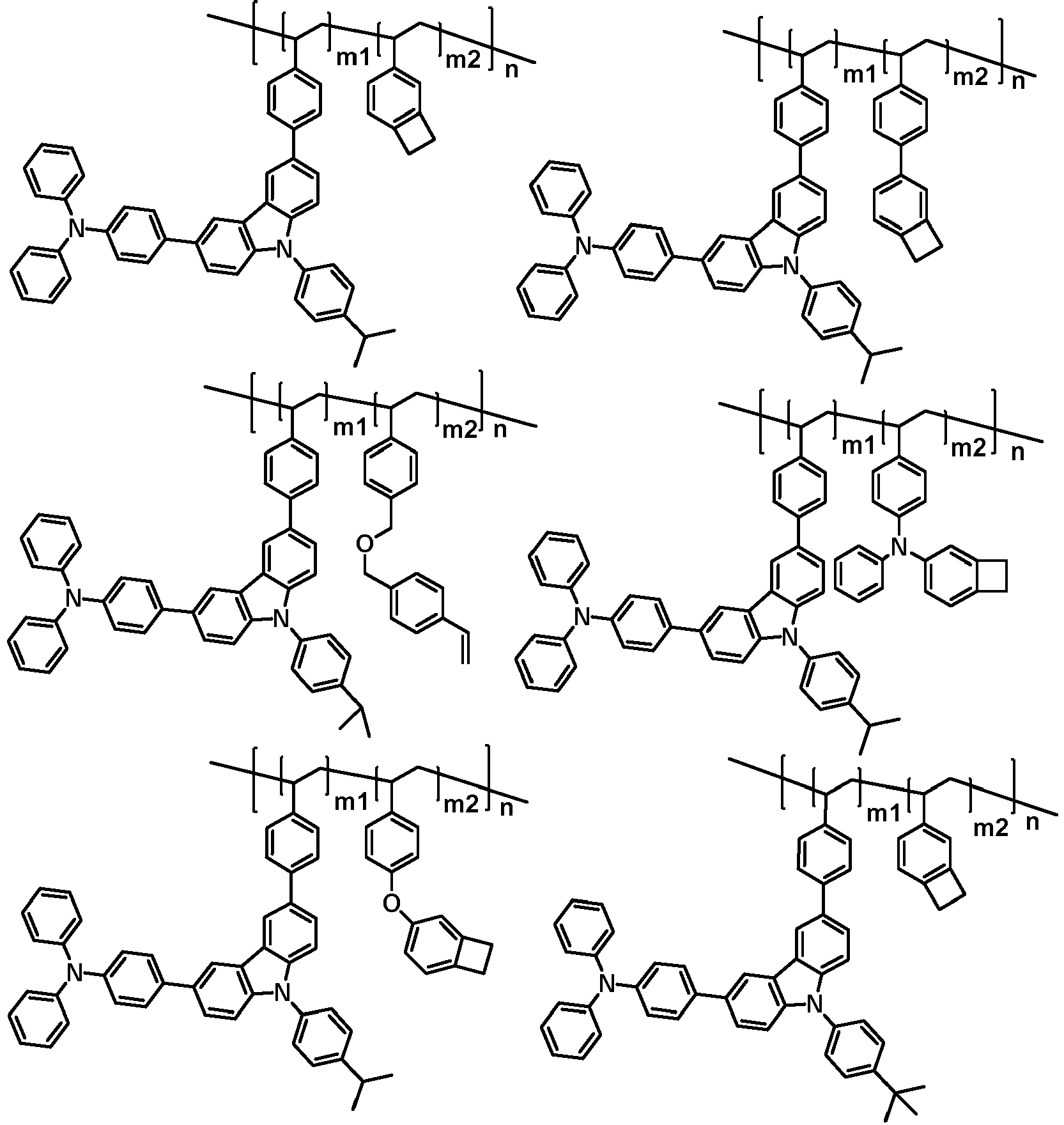
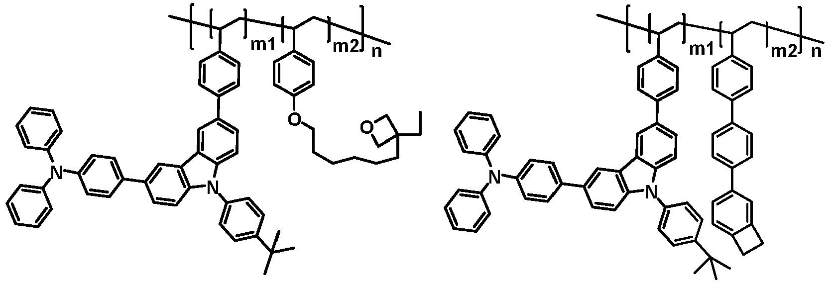

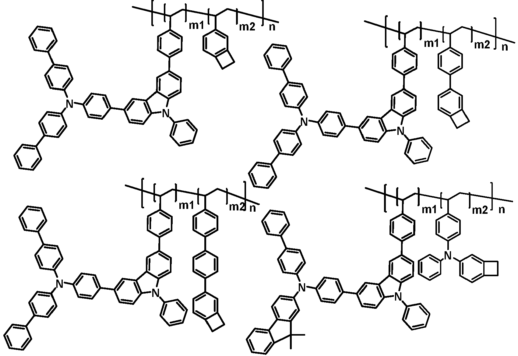
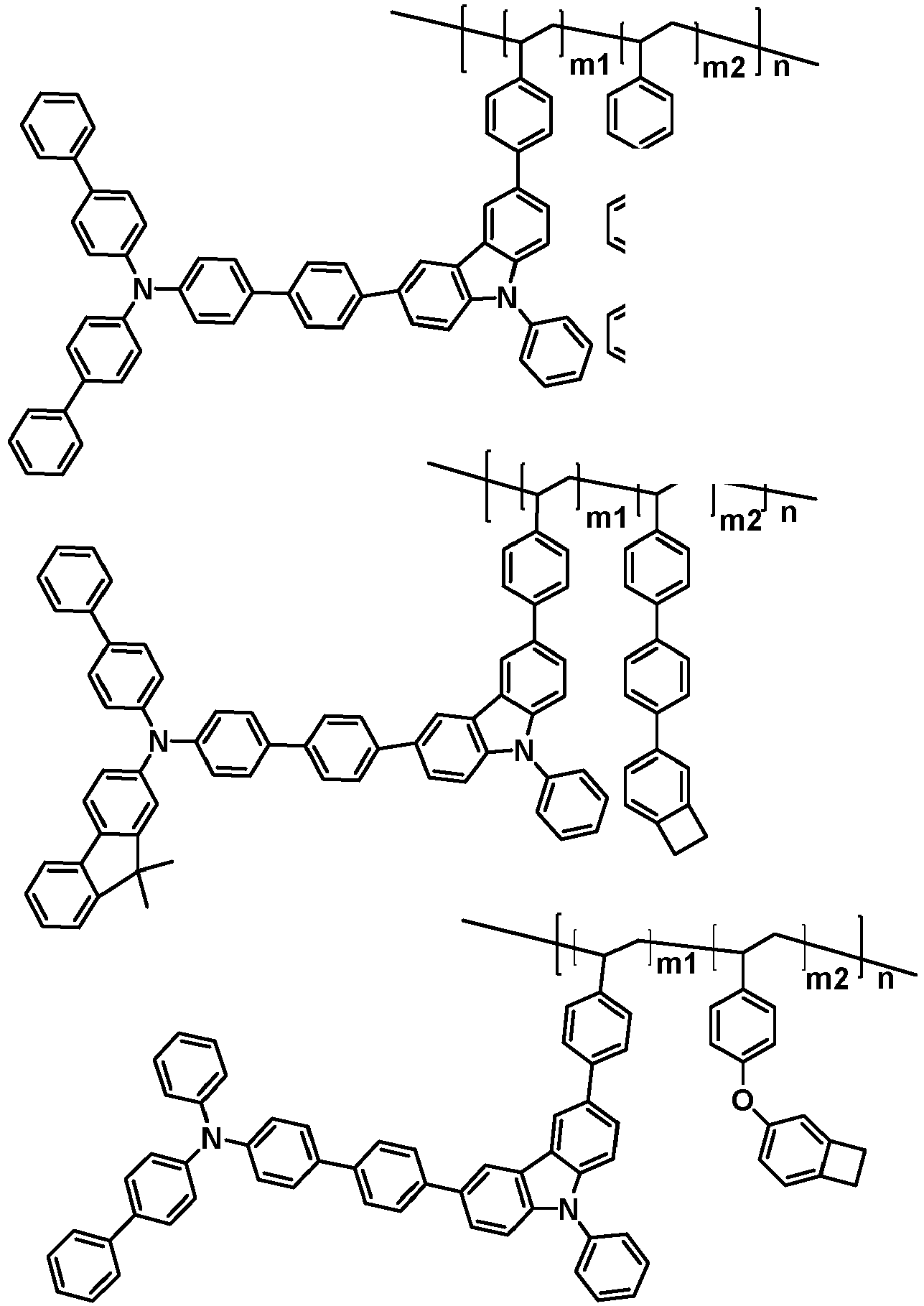


 ist m1 ein Molanteil und 0 < m1 < 1,m2 ist ein Molanteil und 0 < m2 < 1,m1 + m2 ≤ 1 undn ist eine Antzahl der Wiederholungseinheiten und eine ganze Zahl von 1 bis 10.000.
 - Polymer gemäß Anspruch 1, wobei das Polymer ein zahlengemitteltes Molekulargewicht von 5.000 g/mol bis 1.000.000 g/mol aufweist.
- Beschichtungszusammensetzung, umfassend das Polymer gemäß einem der Ansprüche 1 bis 8.
- Beschichtungszusammensetzung gemäß Anspruch 9, ferner umfassend:
ein p-Dotiermaterial. - Organische lichtemittierende Vorrichtung, umfassend:eine erste Elektrode,eine zweite Elektrode, die so angeordnet ist, dass sie der ersten Elektrode gegenübersteht, undeine organische Materialschicht mit einer oder mehreren Schichten, die zwischen der ersten Elektrode und der zweiten Elektrode angeordnet sind,wobei eine oder mehrere Schichten der organischen Materialschicht ein gehärtetes Produkt von der Beschichtungszusammensetzung gemäß Anspruch 9 umfasst.
- Organische lichtemittierende Vorrichtung gemäß Anspruch 11, wobei das gehärtete Produkt von der Beschichtungszusammensetzung in einem Zustand vorliegt, in dem die Beschichtungszusammensetzung durch eine Wärmebehandlung oder eine Lichtbehandlung gehärtet ist.
- Organische lichtemittierende Vorrichtung gemäß Anspruch 11, wobei die organische Materialschicht, die das gehärtete Produkt von der Beschichtungszusammensetzung umfasst, eine Lochtransportschicht, eine Lochinjektionsschicht oder eine Schicht, die gleichzeitig Löcher transportiert und injiziert, ist.
- Organische lichtemittierende Vorrichtung gemäß Anspruch 11, wobei die organische Materialschicht, die das gehärtete Produkt von der Beschichtungszusammensetzung umfasst, eine lichtemittierende Schicht umfasst und die lichtemittierende Schicht das gehärtete Produkt von der Beschichtungszusammensetzung umfasst.
Applications Claiming Priority (2)
| Application Number | Priority Date | Filing Date | Title |
|---|---|---|---|
| KR20180024565 | 2018-02-28 | ||
| PCT/KR2019/002410 WO2019168365A1 (ko) | 2018-02-28 | 2019-02-28 | 중합체, 이를 포함하는 코팅 조성물 및 이를 이용한 유기 발광 소자 |
Publications (3)
| Publication Number | Publication Date |
|---|---|
| EP3680261A1 EP3680261A1 (de) | 2020-07-15 |
| EP3680261A4 EP3680261A4 (de) | 2020-12-16 |
| EP3680261B1 true EP3680261B1 (de) | 2023-04-19 |
Family
ID=67805021
Family Applications (1)
| Application Number | Title | Priority Date | Filing Date |
|---|---|---|---|
| EP19760366.5A Active EP3680261B1 (de) | 2018-02-28 | 2019-02-28 | Polymer, beschichtungszusammensetzung damit und organisches lichtemittierendes element damit |
Country Status (6)
| Country | Link |
|---|---|
| US (1) | US11498987B2 (de) |
| EP (1) | EP3680261B1 (de) |
| JP (1) | JP7034446B2 (de) |
| KR (1) | KR102183737B1 (de) |
| CN (1) | CN111133014B (de) |
| WO (1) | WO2019168365A1 (de) |
Families Citing this family (6)
| Publication number | Priority date | Publication date | Assignee | Title |
|---|---|---|---|---|
| CN111164113B (zh) * | 2018-02-28 | 2022-10-11 | 株式会社Lg化学 | 聚合物、包含其的涂覆组合物和使用其的有机发光元件 |
| JP7558612B2 (ja) * | 2020-01-13 | 2024-10-01 | エルジー・ケム・リミテッド | 重合体およびこれを用いた有機発光素子 |
| CN115108893A (zh) * | 2022-07-29 | 2022-09-27 | 武汉迪赛环保新材料股份有限公司 | 一种苯醚类苯并环丁烯单体及其合成方法 |
| CN115961298B (zh) * | 2022-12-31 | 2024-10-01 | 广西师范大学 | 一种电化学介导乙烯基苯胺与醇合成2,3-二烷氧基取代吲哚啉化合物、合成方法及应用 |
| TW202600500A (zh) * | 2024-03-15 | 2026-01-01 | 德商默克專利有限公司 | 可硬化之組成物 |
| CN121021945A (zh) * | 2025-10-29 | 2025-11-28 | 郴州功田电子陶瓷技术有限公司 | 一种高频高速树脂组合物、包含其的电路材料和印刷电路板 |
Family Cites Families (23)
| Publication number | Priority date | Publication date | Assignee | Title |
|---|---|---|---|---|
| AU2003230308A1 (en) | 2002-05-07 | 2003-11-11 | Lg Chem, Ltd. | New organic compounds for electroluminescence and organic electroluminescent devices using the same |
| US20060142520A1 (en) * | 2004-12-27 | 2006-06-29 | 3M Innovative Properties Company | Hole transport layers for organic electroluminescent devices |
| KR101136878B1 (ko) | 2009-11-11 | 2012-04-20 | 광주과학기술원 | 기능성 블록공중합체-나노입자 복합체 및 이를 이용한 유기전자소자 |
| US8945726B2 (en) * | 2010-02-26 | 2015-02-03 | Nippon Steel & Sumikin Chemical Co., Ltd. | Polymer for organic electroluminescent element, and organic electroluminescent element using the same |
| JP2012111719A (ja) | 2010-11-25 | 2012-06-14 | Idemitsu Kosan Co Ltd | 重合性単量体、その重合体を含む有機デバイス用材料、正孔注入輸送材料及び有機エレクトロルミネッセンス素子用材料、並びに有機エレクトロルミネッセンス素子 |
| JP2012146811A (ja) | 2011-01-12 | 2012-08-02 | Showa Denko Kk | 有機エレクトロルミネッセント素子 |
| EP2692751B1 (de) * | 2011-03-31 | 2015-09-23 | Nippon Steel & Sumikin Chemical Co., Ltd. | Polymer für organische elektrolumineszenzelemente und organisches elektrolumineszenzelement mit einem gehärteten produkt daraus |
| WO2013096918A1 (en) | 2011-12-22 | 2013-06-27 | Georgia Tech Research Corporation | Crosslinking triscarbazole hole transport polymers |
| US20160025998A1 (en) | 2014-07-22 | 2016-01-28 | Greg RUHLAND | Device for rapid detachment of eyewear |
| KR102224495B1 (ko) * | 2014-09-23 | 2021-03-09 | 덕산네오룩스 주식회사 | 유기전기 소자용 화합물, 이를 이용한 유기전기소자 및 그 전자 장치 |
| US10308735B2 (en) | 2014-12-18 | 2019-06-04 | Samsung Electronics Co., Ltd. | Material for organic light-emitting device and organic light-emitting device including the same |
| US10319912B2 (en) * | 2015-01-29 | 2019-06-11 | Samsung Electronics Co., Ltd. | Charge-transporting material and organic light-emitting device including the same |
| KR102455434B1 (ko) * | 2015-01-29 | 2022-10-17 | 삼성전자주식회사 | 전하 수송 재료 및 이를 포함한 유기 발광 소자 |
| WO2016159293A1 (ja) | 2015-03-31 | 2016-10-06 | 出光興産株式会社 | 共重合体、電子素子用材料、有機エレクトロルミネッセンス素子用材料及び有機エレクトロルミネッセンス素子 |
| WO2017031622A1 (en) * | 2015-08-21 | 2017-03-02 | Dow Global Technologies Llc | Polymeric charge transfer layer and organic electronic device containing same |
| KR20180071277A (ko) | 2015-10-16 | 2018-06-27 | 다우 글로벌 테크놀로지스 엘엘씨 | 유기 전하 수송 막을 제조하는 방법 |
| US20210210691A1 (en) | 2015-12-24 | 2021-07-08 | Dow Global Technologies Llc | Polymeric layer and organic electronic device comprising same. |
| KR102087319B1 (ko) * | 2016-03-24 | 2020-05-27 | 덕산네오룩스 주식회사 | 유기전기소자용 화합물, 이를 이용한 유기전기소자 및 그 전자 장치 |
| JP7068199B2 (ja) | 2016-06-28 | 2022-05-16 | ダウ グローバル テクノロジーズ エルエルシー | 量子ドット発光素子 |
| JP2019519943A (ja) | 2016-06-28 | 2019-07-11 | ダウ グローバル テクノロジーズ エルエルシー | 有機電荷輸送膜を作製するためのプロセス |
| US20190202975A1 (en) | 2016-06-28 | 2019-07-04 | Dow Global Technologies Llc | Process for making an organic charge transporting film |
| US20190207169A1 (en) | 2016-06-28 | 2019-07-04 | Dow Global Technologies Llc | Process for making an organic charge transporting film |
| KR20180024565A (ko) | 2016-08-30 | 2018-03-08 | 현대엘리베이터주식회사 | 공공 재난정보를 이용한 엘리베이터 비상제어 시스템 및 그 제어방법 |
-
2019
- 2019-02-28 WO PCT/KR2019/002410 patent/WO2019168365A1/ko not_active Ceased
- 2019-02-28 CN CN201980004720.6A patent/CN111133014B/zh active Active
- 2019-02-28 KR KR1020190023878A patent/KR102183737B1/ko active Active
- 2019-02-28 EP EP19760366.5A patent/EP3680261B1/de active Active
- 2019-02-28 JP JP2020517984A patent/JP7034446B2/ja active Active
- 2019-02-28 US US16/650,697 patent/US11498987B2/en active Active
Also Published As
| Publication number | Publication date |
|---|---|
| CN111133014A (zh) | 2020-05-08 |
| CN111133014B (zh) | 2022-10-11 |
| JP2020535288A (ja) | 2020-12-03 |
| US20200321529A1 (en) | 2020-10-08 |
| KR20190103993A (ko) | 2019-09-05 |
| KR102183737B1 (ko) | 2020-11-27 |
| WO2019168365A1 (ko) | 2019-09-06 |
| EP3680261A1 (de) | 2020-07-15 |
| US11498987B2 (en) | 2022-11-15 |
| EP3680261A4 (de) | 2020-12-16 |
| JP7034446B2 (ja) | 2022-03-14 |
Similar Documents
| Publication | Publication Date | Title |
|---|---|---|
| CN109983087B (zh) | 涂覆组合物和有机发光器件 | |
| EP3680261B1 (de) | Polymer, beschichtungszusammensetzung damit und organisches lichtemittierendes element damit | |
| CN111247651B (zh) | 有机发光器件 | |
| CN111936530B (zh) | 聚合物、包含其的涂覆组合物和使用其的有机发光器件 | |
| EP3680262B1 (de) | Polymer, beschichtungszusammensetzung damit und organische leuchtdiode damit | |
| CN108290837A (zh) | 咔唑衍生物和使用其的有机发光器件 | |
| EP3683208B1 (de) | Verbindung, beschichtungszusammensetzung damit und vorrichtung mit organischer lichtemittierender diode | |
| EP3677606B1 (de) | Polymer, beschichtungszusammensetzung damit und organische lichtemittierende vorrichtung damit | |
| EP3680260B1 (de) | Polymer, beschichtungszusammensetzung damit und organisches lichtemittierendes element damit | |
| KR102176877B1 (ko) | 중합체, 이를 포함하는 코팅 조성물 및 이를 이용한 유기 발광 소자 | |
| CN113811554B (zh) | 聚合物、包含其的涂覆组合物、和使用其的有机发光器件 | |
| KR20220041539A (ko) | 단량체, 중합체, 이를 포함하는 코팅 조성물 및 이를 이용한 유기 발광 소자 | |
| KR20210089343A (ko) | 중합체, 이를 포함하는 코팅 조성물 및 이를 이용한 유기 발광 소자 |
Legal Events
| Date | Code | Title | Description |
|---|---|---|---|
| STAA | Information on the status of an ep patent application or granted ep patent |
Free format text: STATUS: THE INTERNATIONAL PUBLICATION HAS BEEN MADE |
|
| PUAI | Public reference made under article 153(3) epc to a published international application that has entered the european phase |
Free format text: ORIGINAL CODE: 0009012 |
|
| STAA | Information on the status of an ep patent application or granted ep patent |
Free format text: STATUS: REQUEST FOR EXAMINATION WAS MADE |
|
| 17P | Request for examination filed |
Effective date: 20200407 |
|
| AK | Designated contracting states |
Kind code of ref document: A1 Designated state(s): AL AT BE BG CH CY CZ DE DK EE ES FI FR GB GR HR HU IE IS IT LI LT LU LV MC MK MT NL NO PL PT RO RS SE SI SK SM TR |
|
| AX | Request for extension of the european patent |
Extension state: BA ME |
|
| A4 | Supplementary search report drawn up and despatched |
Effective date: 20201116 |
|
| RIC1 | Information provided on ipc code assigned before grant |
Ipc: C09D 125/18 20060101ALI20201110BHEP Ipc: H01L 51/56 20060101ALI20201110BHEP Ipc: H01L 51/10 20060101ALI20201110BHEP Ipc: C08F 212/32 20060101AFI20201110BHEP Ipc: C08F 212/14 20060101ALI20201110BHEP Ipc: H01L 51/00 20060101ALI20201110BHEP |
|
| DAV | Request for validation of the european patent (deleted) | ||
| DAX | Request for extension of the european patent (deleted) | ||
| STAA | Information on the status of an ep patent application or granted ep patent |
Free format text: STATUS: EXAMINATION IS IN PROGRESS |
|
| 17Q | First examination report despatched |
Effective date: 20210924 |
|
| GRAP | Despatch of communication of intention to grant a patent |
Free format text: ORIGINAL CODE: EPIDOSNIGR1 |
|
| STAA | Information on the status of an ep patent application or granted ep patent |
Free format text: STATUS: GRANT OF PATENT IS INTENDED |
|
| INTG | Intention to grant announced |
Effective date: 20221220 |
|
| GRAS | Grant fee paid |
Free format text: ORIGINAL CODE: EPIDOSNIGR3 |
|
| GRAA | (expected) grant |
Free format text: ORIGINAL CODE: 0009210 |
|
| STAA | Information on the status of an ep patent application or granted ep patent |
Free format text: STATUS: THE PATENT HAS BEEN GRANTED |
|
| AK | Designated contracting states |
Kind code of ref document: B1 Designated state(s): AL AT BE BG CH CY CZ DE DK EE ES FI FR GB GR HR HU IE IS IT LI LT LU LV MC MK MT NL NO PL PT RO RS SE SI SK SM TR |
|
| REG | Reference to a national code |
Ref country code: GB Ref legal event code: FG4D |
|
| REG | Reference to a national code |
Ref country code: DE Ref legal event code: R096 Ref document number: 602019027785 Country of ref document: DE |
|
| REG | Reference to a national code |
Ref country code: CH Ref legal event code: EP |
|
| REG | Reference to a national code |
Ref country code: IE Ref legal event code: FG4D |
|
| REG | Reference to a national code |
Ref country code: AT Ref legal event code: REF Ref document number: 1561141 Country of ref document: AT Kind code of ref document: T Effective date: 20230515 |
|
| REG | Reference to a national code |
Ref country code: LT Ref legal event code: MG9D |
|
| REG | Reference to a national code |
Ref country code: NL Ref legal event code: MP Effective date: 20230419 |
|
| REG | Reference to a national code |
Ref country code: AT Ref legal event code: MK05 Ref document number: 1561141 Country of ref document: AT Kind code of ref document: T Effective date: 20230419 |
|
| PG25 | Lapsed in a contracting state [announced via postgrant information from national office to epo] |
Ref country code: NL Free format text: LAPSE BECAUSE OF FAILURE TO SUBMIT A TRANSLATION OF THE DESCRIPTION OR TO PAY THE FEE WITHIN THE PRESCRIBED TIME-LIMIT Effective date: 20230419 |
|
| PG25 | Lapsed in a contracting state [announced via postgrant information from national office to epo] |
Ref country code: SE Free format text: LAPSE BECAUSE OF FAILURE TO SUBMIT A TRANSLATION OF THE DESCRIPTION OR TO PAY THE FEE WITHIN THE PRESCRIBED TIME-LIMIT Effective date: 20230419 Ref country code: PT Free format text: LAPSE BECAUSE OF FAILURE TO SUBMIT A TRANSLATION OF THE DESCRIPTION OR TO PAY THE FEE WITHIN THE PRESCRIBED TIME-LIMIT Effective date: 20230821 Ref country code: NO Free format text: LAPSE BECAUSE OF FAILURE TO SUBMIT A TRANSLATION OF THE DESCRIPTION OR TO PAY THE FEE WITHIN THE PRESCRIBED TIME-LIMIT Effective date: 20230719 Ref country code: ES Free format text: LAPSE BECAUSE OF FAILURE TO SUBMIT A TRANSLATION OF THE DESCRIPTION OR TO PAY THE FEE WITHIN THE PRESCRIBED TIME-LIMIT Effective date: 20230419 Ref country code: AT Free format text: LAPSE BECAUSE OF FAILURE TO SUBMIT A TRANSLATION OF THE DESCRIPTION OR TO PAY THE FEE WITHIN THE PRESCRIBED TIME-LIMIT Effective date: 20230419 |
|
| PG25 | Lapsed in a contracting state [announced via postgrant information from national office to epo] |
Ref country code: RS Free format text: LAPSE BECAUSE OF FAILURE TO SUBMIT A TRANSLATION OF THE DESCRIPTION OR TO PAY THE FEE WITHIN THE PRESCRIBED TIME-LIMIT Effective date: 20230419 Ref country code: PL Free format text: LAPSE BECAUSE OF FAILURE TO SUBMIT A TRANSLATION OF THE DESCRIPTION OR TO PAY THE FEE WITHIN THE PRESCRIBED TIME-LIMIT Effective date: 20230419 Ref country code: LV Free format text: LAPSE BECAUSE OF FAILURE TO SUBMIT A TRANSLATION OF THE DESCRIPTION OR TO PAY THE FEE WITHIN THE PRESCRIBED TIME-LIMIT Effective date: 20230419 Ref country code: LT Free format text: LAPSE BECAUSE OF FAILURE TO SUBMIT A TRANSLATION OF THE DESCRIPTION OR TO PAY THE FEE WITHIN THE PRESCRIBED TIME-LIMIT Effective date: 20230419 Ref country code: IS Free format text: LAPSE BECAUSE OF FAILURE TO SUBMIT A TRANSLATION OF THE DESCRIPTION OR TO PAY THE FEE WITHIN THE PRESCRIBED TIME-LIMIT Effective date: 20230819 Ref country code: HR Free format text: LAPSE BECAUSE OF FAILURE TO SUBMIT A TRANSLATION OF THE DESCRIPTION OR TO PAY THE FEE WITHIN THE PRESCRIBED TIME-LIMIT Effective date: 20230419 Ref country code: GR Free format text: LAPSE BECAUSE OF FAILURE TO SUBMIT A TRANSLATION OF THE DESCRIPTION OR TO PAY THE FEE WITHIN THE PRESCRIBED TIME-LIMIT Effective date: 20230720 Ref country code: AL Free format text: LAPSE BECAUSE OF FAILURE TO SUBMIT A TRANSLATION OF THE DESCRIPTION OR TO PAY THE FEE WITHIN THE PRESCRIBED TIME-LIMIT Effective date: 20230419 |
|
| PG25 | Lapsed in a contracting state [announced via postgrant information from national office to epo] |
Ref country code: FI Free format text: LAPSE BECAUSE OF FAILURE TO SUBMIT A TRANSLATION OF THE DESCRIPTION OR TO PAY THE FEE WITHIN THE PRESCRIBED TIME-LIMIT Effective date: 20230419 |
|
| PG25 | Lapsed in a contracting state [announced via postgrant information from national office to epo] |
Ref country code: SK Free format text: LAPSE BECAUSE OF FAILURE TO SUBMIT A TRANSLATION OF THE DESCRIPTION OR TO PAY THE FEE WITHIN THE PRESCRIBED TIME-LIMIT Effective date: 20230419 |
|
| REG | Reference to a national code |
Ref country code: DE Ref legal event code: R097 Ref document number: 602019027785 Country of ref document: DE |
|
| PG25 | Lapsed in a contracting state [announced via postgrant information from national office to epo] |
Ref country code: SM Free format text: LAPSE BECAUSE OF FAILURE TO SUBMIT A TRANSLATION OF THE DESCRIPTION OR TO PAY THE FEE WITHIN THE PRESCRIBED TIME-LIMIT Effective date: 20230419 Ref country code: SK Free format text: LAPSE BECAUSE OF FAILURE TO SUBMIT A TRANSLATION OF THE DESCRIPTION OR TO PAY THE FEE WITHIN THE PRESCRIBED TIME-LIMIT Effective date: 20230419 Ref country code: RO Free format text: LAPSE BECAUSE OF FAILURE TO SUBMIT A TRANSLATION OF THE DESCRIPTION OR TO PAY THE FEE WITHIN THE PRESCRIBED TIME-LIMIT Effective date: 20230419 Ref country code: EE Free format text: LAPSE BECAUSE OF FAILURE TO SUBMIT A TRANSLATION OF THE DESCRIPTION OR TO PAY THE FEE WITHIN THE PRESCRIBED TIME-LIMIT Effective date: 20230419 Ref country code: DK Free format text: LAPSE BECAUSE OF FAILURE TO SUBMIT A TRANSLATION OF THE DESCRIPTION OR TO PAY THE FEE WITHIN THE PRESCRIBED TIME-LIMIT Effective date: 20230419 Ref country code: CZ Free format text: LAPSE BECAUSE OF FAILURE TO SUBMIT A TRANSLATION OF THE DESCRIPTION OR TO PAY THE FEE WITHIN THE PRESCRIBED TIME-LIMIT Effective date: 20230419 |
|
| PLBE | No opposition filed within time limit |
Free format text: ORIGINAL CODE: 0009261 |
|
| STAA | Information on the status of an ep patent application or granted ep patent |
Free format text: STATUS: NO OPPOSITION FILED WITHIN TIME LIMIT |
|
| 26N | No opposition filed |
Effective date: 20240122 |
|
| PG25 | Lapsed in a contracting state [announced via postgrant information from national office to epo] |
Ref country code: SI Free format text: LAPSE BECAUSE OF FAILURE TO SUBMIT A TRANSLATION OF THE DESCRIPTION OR TO PAY THE FEE WITHIN THE PRESCRIBED TIME-LIMIT Effective date: 20230419 |
|
| PG25 | Lapsed in a contracting state [announced via postgrant information from national office to epo] |
Ref country code: SI Free format text: LAPSE BECAUSE OF FAILURE TO SUBMIT A TRANSLATION OF THE DESCRIPTION OR TO PAY THE FEE WITHIN THE PRESCRIBED TIME-LIMIT Effective date: 20230419 Ref country code: IT Free format text: LAPSE BECAUSE OF FAILURE TO SUBMIT A TRANSLATION OF THE DESCRIPTION OR TO PAY THE FEE WITHIN THE PRESCRIBED TIME-LIMIT Effective date: 20230419 |
|
| PG25 | Lapsed in a contracting state [announced via postgrant information from national office to epo] |
Ref country code: MC Free format text: LAPSE BECAUSE OF FAILURE TO SUBMIT A TRANSLATION OF THE DESCRIPTION OR TO PAY THE FEE WITHIN THE PRESCRIBED TIME-LIMIT Effective date: 20230419 |
|
| REG | Reference to a national code |
Ref country code: CH Ref legal event code: PL |
|
| PG25 | Lapsed in a contracting state [announced via postgrant information from national office to epo] |
Ref country code: LU Free format text: LAPSE BECAUSE OF NON-PAYMENT OF DUE FEES Effective date: 20240228 |
|
| PG25 | Lapsed in a contracting state [announced via postgrant information from national office to epo] |
Ref country code: CH Free format text: LAPSE BECAUSE OF NON-PAYMENT OF DUE FEES Effective date: 20240229 |
|
| PG25 | Lapsed in a contracting state [announced via postgrant information from national office to epo] |
Ref country code: LU Free format text: LAPSE BECAUSE OF NON-PAYMENT OF DUE FEES Effective date: 20240228 Ref country code: CH Free format text: LAPSE BECAUSE OF NON-PAYMENT OF DUE FEES Effective date: 20240229 |
|
| PG25 | Lapsed in a contracting state [announced via postgrant information from national office to epo] |
Ref country code: BG Free format text: LAPSE BECAUSE OF FAILURE TO SUBMIT A TRANSLATION OF THE DESCRIPTION OR TO PAY THE FEE WITHIN THE PRESCRIBED TIME-LIMIT Effective date: 20230419 |
|
| PG25 | Lapsed in a contracting state [announced via postgrant information from national office to epo] |
Ref country code: BG Free format text: LAPSE BECAUSE OF FAILURE TO SUBMIT A TRANSLATION OF THE DESCRIPTION OR TO PAY THE FEE WITHIN THE PRESCRIBED TIME-LIMIT Effective date: 20230419 |
|
| REG | Reference to a national code |
Ref country code: BE Ref legal event code: MM Effective date: 20240229 |
|
| PG25 | Lapsed in a contracting state [announced via postgrant information from national office to epo] |
Ref country code: BE Free format text: LAPSE BECAUSE OF NON-PAYMENT OF DUE FEES Effective date: 20240229 |
|
| PG25 | Lapsed in a contracting state [announced via postgrant information from national office to epo] |
Ref country code: IE Free format text: LAPSE BECAUSE OF NON-PAYMENT OF DUE FEES Effective date: 20240228 |
|
| PG25 | Lapsed in a contracting state [announced via postgrant information from national office to epo] |
Ref country code: IE Free format text: LAPSE BECAUSE OF NON-PAYMENT OF DUE FEES Effective date: 20240228 Ref country code: BE Free format text: LAPSE BECAUSE OF NON-PAYMENT OF DUE FEES Effective date: 20240229 |
|
| PG25 | Lapsed in a contracting state [announced via postgrant information from national office to epo] |
Ref country code: CY Free format text: LAPSE BECAUSE OF FAILURE TO SUBMIT A TRANSLATION OF THE DESCRIPTION OR TO PAY THE FEE WITHIN THE PRESCRIBED TIME-LIMIT; INVALID AB INITIO Effective date: 20190228 |
|
| PG25 | Lapsed in a contracting state [announced via postgrant information from national office to epo] |
Ref country code: HU Free format text: LAPSE BECAUSE OF FAILURE TO SUBMIT A TRANSLATION OF THE DESCRIPTION OR TO PAY THE FEE WITHIN THE PRESCRIBED TIME-LIMIT; INVALID AB INITIO Effective date: 20190228 |
|
| PG25 | Lapsed in a contracting state [announced via postgrant information from national office to epo] |
Ref country code: TR Free format text: LAPSE BECAUSE OF FAILURE TO SUBMIT A TRANSLATION OF THE DESCRIPTION OR TO PAY THE FEE WITHIN THE PRESCRIBED TIME-LIMIT Effective date: 20230419 |
|
| PGFP | Annual fee paid to national office [announced via postgrant information from national office to epo] |
Ref country code: GB Payment date: 20260122 Year of fee payment: 8 |
|
| PGFP | Annual fee paid to national office [announced via postgrant information from national office to epo] |
Ref country code: DE Payment date: 20260120 Year of fee payment: 8 |
|
| PGFP | Annual fee paid to national office [announced via postgrant information from national office to epo] |
Ref country code: FR Payment date: 20260121 Year of fee payment: 8 |