EP3680904B1 - Detektionsschaltkreis eines vorherrschenden dateninhalts in einer speicherzelle - Google Patents
Detektionsschaltkreis eines vorherrschenden dateninhalts in einer speicherzelle Download PDFInfo
- Publication number
- EP3680904B1 EP3680904B1 EP20151007.0A EP20151007A EP3680904B1 EP 3680904 B1 EP3680904 B1 EP 3680904B1 EP 20151007 A EP20151007 A EP 20151007A EP 3680904 B1 EP3680904 B1 EP 3680904B1
- Authority
- EP
- European Patent Office
- Prior art keywords
- transistor
- cells
- read
- test
- circuit
- Prior art date
- Legal status (The legal status is an assumption and is not a legal conclusion. Google has not performed a legal analysis and makes no representation as to the accuracy of the status listed.)
- Active
Links
Images


Classifications
-
- G—PHYSICS
- G11—INFORMATION STORAGE
- G11C—STATIC STORES
- G11C7/00—Arrangements for writing information into, or reading information out from, a digital store
- G11C7/10—Input/output [I/O] data interface arrangements, e.g. I/O data control circuits, I/O data buffers
- G11C7/1006—Data managing, e.g. manipulating data before writing or reading out, data bus switches or control circuits therefor
-
- G—PHYSICS
- G11—INFORMATION STORAGE
- G11C—STATIC STORES
- G11C11/00—Digital stores characterised by the use of particular electric or magnetic storage elements; Storage elements therefor
- G11C11/21—Digital stores characterised by the use of particular electric or magnetic storage elements; Storage elements therefor using electric elements
- G11C11/34—Digital stores characterised by the use of particular electric or magnetic storage elements; Storage elements therefor using electric elements using semiconductor devices
- G11C11/40—Digital stores characterised by the use of particular electric or magnetic storage elements; Storage elements therefor using electric elements using semiconductor devices using transistors
- G11C11/41—Digital stores characterised by the use of particular electric or magnetic storage elements; Storage elements therefor using electric elements using semiconductor devices using transistors forming static cells with positive feedback, i.e. cells not needing refreshing or charge regeneration, e.g. bistable multivibrator or Schmitt trigger
- G11C11/413—Auxiliary circuits, e.g. for addressing, decoding, driving, writing, sensing, timing or power reduction
- G11C11/417—Auxiliary circuits, e.g. for addressing, decoding, driving, writing, sensing, timing or power reduction for memory cells of the field-effect type
- G11C11/419—Read-write [R-W] circuits
-
- G—PHYSICS
- G11—INFORMATION STORAGE
- G11C—STATIC STORES
- G11C16/00—Erasable programmable read-only memories
- G11C16/02—Erasable programmable read-only memories electrically programmable
- G11C16/06—Auxiliary circuits, e.g. for writing into memory
- G11C16/24—Bit-line control circuits
-
- G—PHYSICS
- G11—INFORMATION STORAGE
- G11C—STATIC STORES
- G11C29/00—Checking stores for correct operation ; Subsequent repair; Testing stores during standby or offline operation
- G11C29/04—Detection or location of defective memory elements, e.g. cell constructio details, timing of test signals
- G11C29/08—Functional testing, e.g. testing during refresh, power-on self testing [POST] or distributed testing
- G11C29/12—Built-in arrangements for testing, e.g. built-in self testing [BIST] or interconnection details
- G11C29/14—Implementation of control logic, e.g. test mode decoders
-
- G—PHYSICS
- G11—INFORMATION STORAGE
- G11C—STATIC STORES
- G11C29/00—Checking stores for correct operation ; Subsequent repair; Testing stores during standby or offline operation
- G11C29/04—Detection or location of defective memory elements, e.g. cell constructio details, timing of test signals
- G11C29/08—Functional testing, e.g. testing during refresh, power-on self testing [POST] or distributed testing
- G11C29/12—Built-in arrangements for testing, e.g. built-in self testing [BIST] or interconnection details
- G11C29/18—Address generation devices; Devices for accessing memories, e.g. details of addressing circuits
- G11C29/24—Accessing extra cells, e.g. dummy cells or redundant cells
-
- G—PHYSICS
- G11—INFORMATION STORAGE
- G11C—STATIC STORES
- G11C29/00—Checking stores for correct operation ; Subsequent repair; Testing stores during standby or offline operation
- G11C29/04—Detection or location of defective memory elements, e.g. cell constructio details, timing of test signals
- G11C29/08—Functional testing, e.g. testing during refresh, power-on self testing [POST] or distributed testing
- G11C29/12—Built-in arrangements for testing, e.g. built-in self testing [BIST] or interconnection details
- G11C29/18—Address generation devices; Devices for accessing memories, e.g. details of addressing circuits
- G11C29/30—Accessing single arrays
- G11C29/34—Accessing multiple bits simultaneously
-
- G—PHYSICS
- G11—INFORMATION STORAGE
- G11C—STATIC STORES
- G11C29/00—Checking stores for correct operation ; Subsequent repair; Testing stores during standby or offline operation
- G11C29/04—Detection or location of defective memory elements, e.g. cell constructio details, timing of test signals
- G11C29/08—Functional testing, e.g. testing during refresh, power-on self testing [POST] or distributed testing
- G11C29/12—Built-in arrangements for testing, e.g. built-in self testing [BIST] or interconnection details
- G11C29/38—Response verification devices
-
- G—PHYSICS
- G11—INFORMATION STORAGE
- G11C—STATIC STORES
- G11C7/00—Arrangements for writing information into, or reading information out from, a digital store
- G11C7/24—Memory cell safety or protection circuits, e.g. arrangements for preventing inadvertent reading or writing; Status cells; Test cells
-
- G—PHYSICS
- G11—INFORMATION STORAGE
- G11C—STATIC STORES
- G11C29/00—Checking stores for correct operation ; Subsequent repair; Testing stores during standby or offline operation
- G11C29/04—Detection or location of defective memory elements, e.g. cell constructio details, timing of test signals
- G11C29/08—Functional testing, e.g. testing during refresh, power-on self testing [POST] or distributed testing
- G11C29/12—Built-in arrangements for testing, e.g. built-in self testing [BIST] or interconnection details
- G11C2029/1204—Bit line control
Definitions
- the present application relates to the technical field of memory circuits, in particular those provided with memory points comprising one or more complementary and auxiliary read ports making it possible to read on a memory point without affecting its content. It applies in particular to SRAM memories for (“Static Random Access Memory”).
- a digital calculation device such as for example a microprocessor is provided with an internal memory and an arithmetic and logic unit (ALU) suitable for the implementation of basic arithmetic and / or logic operations to process data. data contained in internal memory.
- ALU arithmetic and logic unit
- the predetermined threshold can be adjusted through at least one stage forming an adjustable resistor and coupled to at least the first read node.
- the term "coupled” is used in the present description to denote a direct electrical link or a link via one or more intermediate components (resistance, transistor, etc.).
- Such a test circuit makes it possible to know the content ( ' 1 ' or ' 0 ' ) predominant in a column of memory cells in a single read cycle. Depending on the value of the predetermined threshold, it is possible for example to know whether there is more 25%, 50% or 75% of '1' contained in the column of cells tested.
- test memory cell contributes to the discharge rate of the first bit line and the discharge is typically much faster as there are '1' stored.
- the test circuit makes it possible from the speed or the discharge slope to evaluate the number of logic ' 1 ' present in the column.
- the second bit line is shared by cells of a dummy column, the second storage nodes being storage nodes of dummy memory cells all storing the same logical data, in particular a logical ' 1 '.
- a dummy column is used as a reference for which the rate of discharge of the bit line or of evolution of the second read node is known.
- the first read node can be connected to the circuit stage forming an adjustable resistor and the value of said threshold can be modulated between several predetermined values corresponding to different predetermined resistance values of said stage forming an adjustable resistor.
- this stage forming an adjustable resistance is provided with a set of m transistors each having a respective on or off conduction state and controlled by a control signal of a set of m respective control of the transistors, the transistors being arranged in parallel so that the resistance value of said stage varies, in particular decreases, as a function of the number of transistors turned on among the m transistors.
- the predetermined thresholds can advantageously be respectively 25%, 50%, and 75%.
- the test circuit can be configured to after said test phase, perform a second test phase to indicate whether the proportion of cells in said column storing a given logic level, in particular a logic ' 1 ' , is greater than or not. at least a second predetermined threshold and different from said predetermined threshold.
- the test result signal is produced by means of a voltage comparator integrated into the test circuit and the output of which is activated by means of a trigger signal, said voltage comparator being provided with a first input connected to the first read node and a second input connected to said second read node.
- the first read node can be connected to a first portion of circuit configured to slow down said variation in potential of said first read node.
- This first circuit portion can comprise at least one transistor whose conduction is controlled by a deceleration control signal whose amplitude depends on said number k of cells of said first column whose read ports are activated during said test phase.
- the second read node can also be connected to a second circuit portion configured to slow down said variation in potential of said first read node, said second circuit portion comprising at least one transistor, the conduction of which is controlled by a signal. slowdown control whose amplitude is modulated as a function of the number k of cells of said first column whose read ports are activated.
- a read port of a cell is activated by means of a word line shared by the cells of a same row of cells of the matrix, the matrix of cells comprising several lines and a plurality of associated word lines.
- the test circuit can then further comprise a circuit block for producing the deceleration control signal intended for said first circuit portion and said second circuit portion, said block being provided with a plurality of transistors in parallel, the word lines of said plurality of word lines being respectively connected to the respective gates of said transistors of said block.
- the second bit line is a bit line complementary to the first bit line capable of being coupled to the respectively complementary storage nodes of said first storage nodes of said cells of said first column, and wherein a first circuit stage forming a first adjustable resistor is arranged between the first bit line and the first read node, and wherein a second circuit stage forming a second adjustable resistor is arranged between the complementary bit line and the second read node, the value of said predetermined threshold being adjustable as a function of the values of said first adjustable resistance and of said second adjustable resistance.
- the first transistor of the first stage is identical to the third transistor of said second stage, the fourth transistor of the second stage also preferably being identical to the second transistor of said first stage.
- all of said activation signals form a signal for selecting said threshold, said threshold being selected at a first value of 50% when the first activation signal and said third activation signal are adapted so as to turn on the first transistor and the third transistor, while the second activation signal and the fourth activation signal are adapted so as to block the second transistor and the fourth transistor respectively.
- the test threshold can advantageously be selected at a second value, in particular 25%, when the first activation signal and the fourth activation signal are adapted so as to make the first transistor and the fourth transistor respectively on, while the second activation signal and the third activation signal are provided so as to block the second transistor and the third transistor.
- the test threshold can advantageously be selected at a third value, in particular 75%, when the first activation signal and the fourth activation signal are provided so as to make the first transistor and the fourth transistor respectively blocked, while the second activation signal and the third activation signal are provided so as to pass the second transistor and the third transistor.
- the test result signal can be produced by means of a voltage sense amplifier integrated into said test circuit, said voltage sense amplifier being provided with a first input connected to the first read node and a second input connected to said second read node.
- the test result signal may be recorded at the output of a flip-flop upon receipt of a trigger signal.
- test circuit A particular application of the test circuit consists in using this circuit in order to prevent an attempt to access memory data.
- a test circuit such as implemented according to an embodiment of the present invention and making it possible to know the predominant content in a column of memory cells is integrated into a memory device provided with a memory matrix formed of a plurality of rows cells and one or more columns of memory cells.
- test circuit is implemented without modifying the internal structure of the memory cells and only requires the implementation of a small number of additional peripheral elements to the matrix of cells.
- a memory cell Ci (also called a memory point) of the memory device into which the test circuit is integrated can have an arrangement as illustrated diagrammatically in the diagram. figure 1A .
- the cell Ci shown is provided with at least one storage node T, designed to store a piece of data, typically a ' 1 ' or a '0', as a function of a potential value maintained on this node T.
- the cell Ci also comprises a read port 2 for, when it is activated by means of a word line WL, making it possible to connect the first storage node T to a bit line RBL shared by the cells of a same column (ie a vertical row) of cells as cell Ci.
- the bit line RBL can in particular be a bit line dedicated to read operations on cell Ci.
- Word line WL is typically shared by cells d 'the same row (ie a horizontal row) of cells of the matrix as the cell Ci.
- the read port 2 typically comprises one or more access transistors (not shown in this figure), the conduction of which is controlled by a signal applied to the word line WL.
- Read port 2 is preferably an auxiliary read port or specific to read operations and designed so that when read operation when the bit line RBL is coupled to the storage node T, the logical data stored by the node T is held and is not affected.
- a particular embodiment provides for a memory device formed of SRAM type cells.
- This type of cell is typically provided with two storage nodes T and F, designed to store a first logical datum, and a logical datum complementary to the first datum, the maintenance of the logical data at the nodes T, F being ensured by transistors forming inverters curled on themselves.
- the SRAM cell can in this case be for example a cell with 6 transistors (6T) or else a cell with 8 transistors (8T or 6T + 2T) and provided with a single read port 2 such as for example the one illustrated on the figure. figure 1C .
- a cell provided with two read ports 2 and for example formed of 10 transistors (10T) such as the one illustrated for example on figure 1B can also be provided.
- a read port 2 can be formed from several access transistors 21, 22.
- a first access transistor 3 has its gate connected to a storage node and a second access transistor 4 has its gate connected to a line word RWL this time dedicated to read operations and different from a write word line and its drain connected to a read bit line RBL, RBL T , RBL F which is only used in this example for the read operations and is not used for writing.
- the word line RWL being non-activated, in other words typically at zero potential in the case of an access transistor of the type N, the path between the RBL bit line and ground is cut.
- a read operation on the cell is triggered when the word line RWL is activated, in other words a signal emitted on the latter allows access to the storage node T or F associated with this word line RWL.
- a test circuit such as implemented according to the invention can thus make it possible to evaluate the predominance of the same logical datum in a set of memory cells as described above and belonging to a same column of cells. In particular, one can assess the predominance of cells containing a logical '1' in a column of cells.
- the test circuit is suitable for evaluating whether, among the cells tested in a column of cells, the percentage or the proportion of cells storing the same given logic level, in particular a logic ' 1 ' , is greater than or not.
- at least adjustable predetermined threshold this threshold being able to be fixed for example at 25% or for example at 50% or for example at 75%.
- the predetermined threshold can thus be selected from a plurality of predetermined thresholds, for example between three thresholds: advantageously 25%, 50% and 75%.
- the test circuit is configured to perform such a test phase during a read operation or a read cycle, by performing a simultaneous reading of several tested cells, in other words by providing simultaneous access to the respective read ports. of several cells tested.
- test circuit 10 An exemplary embodiment of such a test circuit 10 as implemented according to a first embodiment of the present invention is given on figure 2 .
- the test circuit 10 is represented here for the sake of simplicity with a single column COL 1 of n memory cells C 1 , ..., C n (with n for example equal to 32) on which it is desired to carry out an occurrence test data in order to determine whether the percentage or the rate of cells storing the same data among the set of all the cells of this column COL 1 or among a group of cells of this column COL 1 is or not greater than a predetermined threshold.
- a statistical test is carried out on the logical data item ' 1 ' by checking, for example, whether or not at least M% of cells store the logical data item '1'.
- the test threshold M is for example set at 50% or at 25% or at 75%.
- the test can be carried out on a predetermined number of k (with 2 ⁇ k ⁇ n) cells of the COL 1 column, depending on the number k of word lines activated simultaneously during this test, among a set of n word lines WL 0 , ..., WL n-1 .
- the test circuit can comprise or be associated with an activation circuit (not shown) which can be integrated into a line decoder associated with the matrix and which is configured to perform an activation circuit. simultaneous activation of word lines, so as to perform a simultaneous selection of different rows of respective read ports of cells of column COL 1 of cells.
- the line decoder can in this case be modified so as to be able to activate several word lines at the same time or even all the word lines at the same time by adding for example an additional input or by using CAM column outputs ("Content Addressable Memories ”).
- Column COL 1 tested is associated with a bit line RBL 1 at the end of which a first read node NL 1 is located .
- the circuit 10 is also provided with a reference column which, in this exemplary embodiment, is a dummy Dum_COL column (in English "dummy") composed of n dummy memory cells (“ dummy cells ”), that is to say which serve as a reference or as control cells rather than as a means in which we have to write data to be stored.
- the dummy cells Dum_C 0 , ... Dum_C n-1 of the dummy column Dum_COL make it possible to produce reference electrical signals.
- the dummy cells are in number n (with n for example equal to 32) equal to that of a column COL1 of the matrix and can have a structure similar to those of the other cells of the memory matrix and for example as described. previously in conjunction with figures 1A-1C .
- the dummy cells Dum_C 0 , .., Dum-C n-1 and their associated storage node are configured so as to store the same logical data, for example a logical '1'.
- the dummy cells can thus be provided with at least one storage node which is constantly forced to a given potential, for example supply voltage VDD, so as to obtain a cell on which it is possible to read access without being able to achieve write access.
- Such dummy cells Dum_C 0 , .., Dum_C n-1 thus make it possible to produce a reference datum which remains the same for all the read accesses and tests carried out.
- the dummy column Dum_COL is associated with a bit line RBL_Dum at the end of which is a second read node NL 2 .
- the first bit line RBL 1 and the bit line RBL_Dum associated with the dummy Dum_COL column are typically pre-loaded via a pre-charge circuit (not shown), for example at a supply potential VDD.
- This pre-charge circuit can be arranged at one end of bit line RBL 1 and at one end of bit line RBL_Dum opposite to that where the first read node NL 1 and the second read node NL 2 are respectively located.
- the preload of bit line RBL 1 is deactivated beforehand.
- the simultaneous activation of k data word lines WL 0 , ..., WL n-1 is deactivated beforehand.
- This activation of the k word lines WL 0 , ..., WL n-1 makes it possible to simultaneously activate the respective k read ports of the cells tested as well as the respective k read ports of the dummy cells.
- Part of the test phase consists in waiting for the bit lines RBL1 and RBL_Dum to discharge, which makes it possible to vary, in this example to increase, the respective potentials of the nodes NL 1 and NL 2 .
- the first node NL 1 has a potential which varies at a rate which depends on the (unknown) number of logic '1' present in the set of k cells of column COL 1 , while the rate of discharge of the dummy column depends the number k (known) of logical ' 1 ' of the k activated cells of the dummy column Dum_COL.
- the respective discharge speeds or slope of nodes NL 1 and NL 2 are used to assess whether the number of logic ' 1 ' in column COL 1 is greater than or not the predetermined threshold, for example 25% or 50% or of 75% of all cells tested in a column.
- the adjustable threshold is set here using a circuit stage 20 forming an adjustable resistor connected to the first read node NL 1 .
- the adjustable resistor is in this example formed of circuit branches coupled to the first read node NL1 and respectively provided with transistors 21, 22, 23, advantageously identical in terms of design and dimensions.
- the transistors 21, 22, 23 are for example of the PMOS type with respective sources connected to a VDD supply, respective gates controlled respectively by the threshold control signals CMD25, CMD50, CMD75.
- a first control signal CMD25 makes it possible to control the on or off conduction state of the transistor 21, while a second threshold control signal CMD50 makes it possible to control the on or off conduction state of transistor 22, and a third threshold CMD75 control signal determines the on or off conduction state of the transistor 21.
- transistor 23 The resistance value is thus adjusted, in particular reduced, as a function of the number of transistors 21, 22, 23 turned on.
- Cumulative activation is implemented.
- a first threshold level for example 25%
- a second threshold level which corresponds to a higher discharge speed of the first bit line RBL1
- the transistors 21, 22 are activated, which in this example makes it possible to reduce the resistance of the stage 20, in Particularly to divide it by 2.
- the transistors 21, 22, 23 are activated, for example to divide the adjustable resistance by 3 and set a threshold at a third level, for example of 75%, which corresponds to an even faster evolution of the resistance.
- first NL1 read node during the test phase.
- the set of control signals CMD25, CMD50, CMD75 thus forms a threshold adjustment signal which may be digital.
- the potential at the second read node NL 2 is established taking into account in particular a setting to GND caused by the k activated read ports.
- a comparison is made of the potential at the first read node NL 1 and at the second read node NL 2 , by means of a voltage comparator 30 provided with a first input connected to the first read node NL1 and with a second input NL2 connected to said second read node, in order to be able to evaluate the potential level of the first read node NL1 in comparison with that of the second serving node NL2 reference.
- An activation signal from comparator 30 also called trigger signal EN determines when its inputs and the result which results from the comparison of its inputs should be taken into account.
- the end of the test operation can be determined arbitrarily, for example by using a circuit containing a delay chain which produces the trigger signal EN according to a delay determined after the start of the test phase. test.
- a reference path including the read circuit and having an adjustable propagation time as a function of various parameters such as the process, the voltage levels involved, in particular the power supply, the temperature, can alternatively be used to generate the trigger signal EN.
- the comparator 30 is used to deliver a logical test result signal S_OUT which, depending on its state ' 1 ' or '0' indicates whether yes (for example state '1') or not (state '0') the proportion of test cells storing the value '1' exceeds the test threshold, for example by 50% cells.
- a portion 40 of the circuit configured to slow down the variation in potential of the first read node NL1 can be provided.
- This portion 40 of the circuit is here provided with transistors 41, 42, 43, for example of the PMOS type, placed in series with the transistors 21, 22, 23 of stage 20 forming an adjustable resistor.
- the conduction of the transistors 41, 42, 43 used for implementing the slowing down is controlled by a slowing control signal SLOW applied to their gate.
- This SLOW signal has an amplitude which depends on the number k of cells of said first column COL 1 , the read ports of which are activated during the test phase.
- a portion 50 of the circuit provided with a transistor 52, for example of the PMOS type. connected to a potential, for example VDD, the conduction of which is controlled by the same slowdown control signal SLOW.
- the block 60 is also formed of n transistors 61 1 , ..., 61 n , for example of the NMOS type, with a common source and a common drain and which are thus arranged in parallel.
- Each of the gates of the transistors is controlled by a specific word line among the n word lines WL 0 , ..., WL n-1 making it possible to read access to the n cells of a column of cells.
- the word lines WL 0 , ..., WL n-1 are thus respectively connected to the respective gates of said n transistors 61 1 , ..., 61 n .
- the SLOW signal taken from the common drain of transistors 61 0 , ..., 61 n-1 therefore depends on the number of word lines WL 0 , ..., WL n-1 activated during the test phase.
- the block 60 is typically also provided with a PMOS transistor 62, serving as a generator and whose drain is connected to the supply VDD, the gate held to ground and the source connected to a node delivering SLOW deceleration control signal.
- the bit line RBL 1 and the reference bit line RBL_dummy are strongly pulled to GND via the read ports, but in this case the SLOW signal very close to GND activates all the transistors 61 1 , ..., 61 n PMOS so as to keep the nodes NL 1 and NL 2 away from GND.
- test result obtained at the end of a test phase implemented during a reading cycle It may be desirable to refine the test result obtained at the end of a test phase implemented during a reading cycle. For this, a sequence of several tests during which the threshold is modified can be implemented.
- a first test is carried out with a first threshold, for example of 25% corresponding to a first set of control signal values CMD25, CMD50, CMD75 which determines a first resistance value of the stage 20 is implemented .
- the variation in potential of the first read node NL1 is thus calibrated in this way when the read ports are activated and the first bit line RBL1 discharges.
- the signal S_OUT indicates that the number of cells storing the value ' 1 ' is greater than 25%
- a second test can be carried out in order to carry out a more precise evaluation of the quantity of '1' stored.
- a second test can then be carried out with a second threshold, for example of 50% corresponding to a second set of control signal values CMD25, CMD50, CMD75 which determines a second resistance value of stage 20.
- a second threshold for example of 50% corresponding to a second set of control signal values CMD25, CMD50, CMD75 which determines a second resistance value of stage 20.
- a third test can then be carried out with a third threshold, for example of 75% corresponding to a third set of control signal values CMD25, CMD50, CM75 which determines a third resistance value of stage 20.
- the signal S_OUT indicates while the number of cells storing the value ' 1 ' is less than 75%.
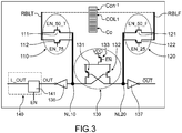
- test circuit An alternative embodiment of a test circuit whose energy consumption is reduced is given on the figure 4 .
- the content of column COL1 of cells C 0 , ..., C n-1 is evaluated using a first bit line RBLT, intended, during a test phase carried out during a read cycle, to be put to the potential of a first storage node of the cells of the first column, and of which the discharge speed is evaluated at the level of a first node NL10 reading coupled to this first RBLT bit line.
- a second RBLF bit line is used, intended during a test phase carried out during a read cycle to be put to potential.
- a second storage node for the cells of the first column complementary to the first node.
- We evaluate the discharge speed of the second bit line RBLF which provides information on the respective potentials of the second storage nodes and therefore on the logical data stored by these second nodes from a second read node NL20 coupled to the second line of RBLF bit.
- the test circuit is this time provided with a first circuit stage 110 forming a first adjustable resistor and which is arranged between one end of the first bit line RBLT and the first read node NL10.
- the first adjustable resistor is produced by means of a transistor 111, for example of the NMOS type, and another transistor 112 in parallel, for example of the NMOS type.
- Transistors 111, 112 have respective drains coupled to the first RBLT bit line and respective sources coupled to the first read node NL10.
- the transistor 111 has a conduction state controlled by an activation signal EN_50_T applied to its gate, while the transistor 112 has a conduction state controlled by another activation signal EN_75 applied to its gate.
- the test circuit is also provided with a second circuit stage 120 forming a second adjustable resistor and which is arranged between one end of the complementary RBLF bit line of column COL 1 and the second read node NL20.
- the second adjustable resistor can also be produced through transistors in parallel, with a transistor 121, for example of the NMOS type, and another transistor 122, for example of the NMOS type, having drains connected to each other and to one end of the resistor.
- the transistor 121 for its part, is made on or off according to an activation signal EN_50_F applied to its gate, while the transistor 122 can be made on or off by means of a signal d 'EN_25 activation applied to its grid.
- the transistors 111, 121 are preferably identical.
- the transistors 112, 122 are also of identical design and size.
- the transistors 112, 122 are provided with different dimensions from those of the transistors 111, 121, in particular with different W / L (width to length of the channel region) ratios.
- the transistors 112, 122 are provided with a width W2 less than that W1 of the transistors 111, 121.
- the test threshold is set at 50%, for example when the test aims to determine whether the column COL1 has a majority of ' 1 ' at the level of the first storage nodes of the cells of this column COL1 , the resistance of the first stage 110 and that of the second stage 120 are made balanced by turning on the transistors 111, 121 while the transistors 112, 122 are not activated.
- the transistors 112, 122 make it possible to establish other test thresholds by creating a resistance imbalance between the first stage 110 and the second stage 120.
- a second test threshold for example 25% is established by turning on the transistor 111 of the first stage 110 and the transistor 122 of the second stage 120, while the transistors 112, 121 are not activated. in other words are put in a blocked state.
- This second configuration where the resistance of the first stage 110 is lower than that of the second stage 120, for example makes it possible to determine whether or not the column COL1 has at least 25% of ' 1 ' at the level of the first storage nodes of the cells. .
- a third test threshold can also be established by turning on the transistor 112 of the first stage 110 and the transistor 121 of the second stage 120, while the transistors 111, 122 are not activated, in other words are in a blocked state.
- This third configuration where the resistance of the first stage 110 is this time greater than that of the second stage 120, for example makes it possible to determine whether or not column COL1 has at least 75% of ' 1 ' at the first storage nodes of the cells.
- the activation signals EN_50_T, EN_50_F, EN_25, EN_75 are typically logic signals.
- the set of activation signals EN_50_T, EN_50_F, EN_25, EN_75 forms a digital threshold selection signal which, in the particular embodiment described above is likely to adopt 3 different states depending on the threshold selected from 3 thresholds of available tests, for example 25%, 50%, 75%. A larger number of thresholds could be considered by increasing the number of transistors of stages 110, 120 and of associated activation signals.
- the discharge of the first bit line is carried out at a speed which depends on the number of logic '1' stored in the set of storage nodes tested and which is different from that of the complementary bit line.
- This difference in line load speed results in an imbalance between the first read node NL10 and the second read node NL20.
- This imbalance is amplified by means of a sense amplifier 130.
- the sense amplifier can be formed by load transistors 131, 132, for example of the PMOS type, connected together crosswise, so that the gate of a load transistor 131 is connected to the second read node NL20, while that the gate of the other load transistor 132 is connected to the first read node NL10, the drain of load transistor 132 being connected to the gate of load transistor 131.
- the transistors 131, 132 are provided with a common source capable of being brought to a supply potential VDD by means of a switch transistor 133 whose conduction depends on the test signal.
- the transistor 133 can be for example a transistor 133 of the PMOS type made through a signal IN complementary to the trigger signal EN.
- a test result signal OUT is output from a first inverter 136 connected to the first read node NL20, while a sample can be taken.
- An asynchronous flip-flop 141 or latch 141 controlled by the trigger signal EN makes it possible to record the value of the test result, in the form of a signal L_OUT.
- evolution curves C_EN, C_NL20, C_NL10, C_OUT, C_OUT_Iatch give examples of evolution curves respectively of the trigger EN signal, of the signal taken at the second node NL20, of the signal taken at the first node NL10, of the signal OUT of output of the first inverter, and of the test result signal at the output of the flip-flop, this for a test carried out on a column of cells comprising more than 50% of cells storing the value '1'.
- evolution curves C'_NL20, C'_NL10, C'_OUT, C'_OUT_latch give examples of evolution curves respectively of the signal taken at the second node NL20, of the signal taken at the first node NL10, of the output signal OUT of the first inverter, and of the test result signal at the output of the flip-flop, this for a test carried out on a column of cells comprising this time less than 50% of cells storing the value '1'.
- test circuit integrated in a memory device and as described above finds applications in particular in the field of image processing.
- a test circuit integrated in a memory device and as described above can be applied to a data protection of the memory.
Landscapes
- Engineering & Computer Science (AREA)
- Microelectronics & Electronic Packaging (AREA)
- Computer Hardware Design (AREA)
- For Increasing The Reliability Of Semiconductor Memories (AREA)
- Static Random-Access Memory (AREA)
- Tests Of Electronic Circuits (AREA)
- Techniques For Improving Reliability Of Storages (AREA)
Claims (17)
- Speichervorrichtung mit einer Matrix von Speicherzellen, wobei die Matrix mit zumindest einer ersten Spalte (COL1) von Zellen (C0, Cn-1) versehen ist, wobei jede der Zellen aufweist:- zumindest einen ersten Speicherknoten (T) zur Speicherung von logischen Daten, insbesondere "1" oder "0", deren Wert demjenigen zumindest eines Potentials am ersten Speicherknoten (T) entspricht,- zumindest einen Leseanschluss (2), um, wenn er aktiviert ist, das Potenzial des ersten Speicherknotens (T) an eine erste Bitleitung (RBL1, RBLT) zu übertragen, die von den Zellen (C0, Cn-1) der ersten Spalte (COL1) von Zellen gemeinsam genutzt wird,dadurch gekennzeichnet, dass sie ferner enthält:
wobei die Vorrichtung ferner mit einer Testschaltung versehen ist, die dazu ausgelegt ist, bei einem Lesevorgang eine Testphase durchzuführen, um anzugeben, ob der Anteil der Zellen in der Spalte (COL1), die dieselben logischen Daten, insbesondere eine logische "1", speichern, größer als zumindest ein vorbestimmter Schwellenwert ist oder nicht, wobei die Testschaltung aufweist:- einen ersten Leseknoten (NL1, NL10), der mit einem Ende der ersten Bitleitung (RBL1, RBLT) gekoppelt ist,- einen zweiten Leseknoten (NL2, NL20), der mit einem Ende einer zweiten Bitleitung (RBL_Dum, RBL2) gekoppelt ist, wobei die zweite Bitleitung eine Referenzbitleitung bildet, die einer Vielzahl von zweiten Logikinformationsspeicherknoten zugeordnet ist, wobei die zweiten Speicherknoten dazu ausgelegt sind, alle dieselbe Logikinformation zu speichern, oder jeweils zu den Zellen der ersten Spalte gehören und zu den ersten Knoten komplementäre Speicherknoten sind,- zumindest eine Stufe (20, 110), die einen einstellbaren Widerstand zum Einstellen des vorbestimmten Schwellenwerts bildet, wobei die Stufe mit zumindest dem ersten Leseknoten gekoppelt ist,
wobei die Testschaltung (10, 100) ausgelegt ist zum:- gleichzeitigen Aktivieren von k jeweiligen Leseanschlüssen einer Anzahl k von Zellen der ersten Spalte bei gleichzeitigem Aktivieren von k weiteren Leseanschlüssen einer entsprechenden Anzahl k von zweiten Speicherknoten, denen diese weiteren Leseanschlüsse zugeordnet sind, um eine Entladung der ersten Bitleitung und eine Entladung der zweiten Bitleitung und folglich eine Potentialänderung an dem ersten Leseknoten und an dem zweiten Leseknoten zu bewirken,
dann nach einer vorbestimmten Zeitspanne als eine Funktion der Potentialdifferenz zwischen dem ersten Leseknoten und dem zweiten Leseknoten- Erzeugen zumindest eines logischen Testergebnissignals (S_OUT, L_OUT), das in Abhängigkeit von seinem Wert angibt, ob der Anteil der Zellen in der Spalte (COL1), die einen gegebenen logischen Pegel, insbesondere eine logische "1", speichern, über dem vorbestimmten Schwellenwert liegt oder nicht. - Speichervorrichtung nach Anspruch 1, wobei die zweite Bitleitung von Zellen einer Dummy-Spalte (Dum_COL) gemeinsam genutzt wird, wobei die zweiten Speicherknoten Speicherknoten von Dummy-Speicherzellen (Dum_CO, ... Dum_Cn-1) sind, die alle die gleichen logischen Daten, insbesondere eine logische "1", speichern.
- Speichervorrichtung nach Anspruch 2, wobei der erste Leseknoten (NL1) mit der Schaltungsstufe (20) verbunden ist, die einen einstellbaren Widerstand bildet, wobei der Wert des Schwellenwerts zwischen mehreren vorbestimmten Werten modulierbar ist, die verschiedenen vorbestimmten Widerstandswerten der Stufe (20) entsprechen.
- Speichervorrichtung nach Anspruch 3, wobei die einen einstellbaren Widerstand bildende Schaltungsstufe (20) mit einem Satz von m Transistoren (21, 22, 23) versehen ist, von denen jeder einen entsprechenden Ein- oder Aus-Leitungszustand aufweist und jeweils durch ein Steuersignal eines Satzes von m Steuersignalen (CMD25, CMD50, CM75) der Transistoren (21, 22, 23) gesteuert wird, wobei die Transistoren parallel geschaltet sind, so dass der Widerstandswert der genannten Stufe in Abhängigkeit von der Anzahl der eingeschalteten Transistoren unter den m Transistoren variiert, insbesondere abnimmt.
- Speichervorrichtung nach Anspruch 4, wobei der Satz von Steuersignalen (CMD25, CMD50, CM75) ein digitales Auswahlsignal mit m Zuständen des genannten Schwellenwerts bildet, insbesondere mit m=3, wobei die vorbestimmten Schwellenwerte vorteilhafterweise 25%, 50% bzw. 75% betragen.
- Vorrichtung nach einem der Ansprüche 2 bis 5, wobei die Testschaltung dazu ausgelegt ist, nach der Testphase eine zweite Testphase durchzuführen, um anzugeben, ob der Anteil der Zellen in der Spalte, die einen gegebenen logischen Pegel, insbesondere eine logische "1", speichern, größer als zumindest ein zweiter vorbestimmter Schwellenwert, der sich von dem ersten Schwellenwert unterscheidet, ist oder nicht.
- Speichervorrichtung nach einem der Ansprüche 2 bis 6, wobei das Testergebnissignal (S_OUT) mittels eines in der Testschaltung integrierten Spannungskomparators (30) erzeugt wird, dessen Ausgang mittels eines Triggersignals (EN) aktiviert wird, wobei der Spannungskomparator mit einem ersten Eingang, der mit dem ersten Leseknoten (NL1) verbunden ist, und mit einem zweiten Eingang, der mit dem zweiten Leseknoten (NL2) verbunden ist, versehen ist.
- Vorrichtung nach einem der Ansprüche 2 bis 7, wobei der erste Leseknoten (NL1) mit einem ersten Schaltungsabschnitt (40) verbunden ist, der dazu ausgelegt ist, die Potentialänderung des ersten Leseknotens (NL1) zu verlangsamen, wobei der erste Schaltungsabschnitt (40) zumindest einen Transistor (41, 42, 43) umfasst, dessen Leitung durch ein Verlangsamungssteuersignal (SLOW) gesteuert wird, dessen Amplitude von der Anzahl k der Zellen der ersten Spalte (COL1) abhängt, deren Leseanschlüsse während der Testphase aktiviert werden.
- Vorrichtung nach einem der Ansprüche 2 bis 8, wobei der zweite Leseknoten (NL2) mit einem zweiten Schaltungsabschnitt (50) verbunden ist, der dazu ausgelegt ist, die Potentialänderung des ersten Leseknotens zu verlangsamen, wobei der zweite Schaltungsabschnitt (50) zumindest einen Transistor (51) umfasst, dessen Leitung durch ein Verlangsamungssteuersignal (SLOW) gesteuert wird, dessen Amplitude in Abhängigkeit von der Anzahl k der Zellen der ersten Spalte, deren Leseanschlüsse aktiviert sind, moduliert wird.
- Vorrichtung nach Anspruch 9, wobei ein Leseanschluss einer Zelle über eine Wortleitung aktiviert wird, die von den Zellen einer gleichen Zeile von Zellen der Matrix gemeinsam genutzt wird, und wobei die Matrix von Zellen mehrere Zeilen und eine Vielzahl von zugeordneten Wortleitungen (WL0, ..., WLn-1) umfasst, wobei die Testschaltung ferner einen Schaltungsblock (60) zum Erzeugen des Verlangsamungssteuersignals (SLOW) für den Transistor (41, 42, 43) des ersten Schaltungsabschnitts (40) und den Transistor (51) des zweiten Schaltungsabschnitts (50) aufweist, wobei der Schaltungsblock (60) mit einer Vielzahl von parallel geschalteten Transistoren (610, ..., 61n-1) versehen ist, wobei die Wortleitungen (WL0, ..., WLn-1) der Vielzahl von Wortleitungen (WL) jeweils mit den entsprechenden Gates der Transistoren des Blocks (60) verbunden sind.
- Speichervorrichtung nach Anspruch 1, wobei die zweite Bitleitung eine komplementäre Bitleitung (RBLF) zur ersten Bitleitung (RBLT) ist, die mit den jeweils komplementären Speicherknoten der ersten Speicherknoten der Zellen der ersten Spalte (COL1) gekoppelt werden kann, und wobei eine erste Schaltungsstufe (110), die einen ersten einstellbaren Widerstand bildet, zwischen der ersten Bitleitung (RBLT) und dem ersten Leseknoten (NL10) geschaltet ist, und wobei eine zweite Schaltungsstufe (120), die einen zweiten einstellbaren Widerstand bildet, zwischen der komplementären Bitleitung (RBLF) und dem zweiten Leseknoten (NL10) geschaltet ist, wobei der Wert des Schwellenwerts in Abhängigkeit von den Werten des ersten einstellbaren Widerstands und des zweiten einstellbaren Widerstands modulierbar ist.
- Speichervorrichtung nach Anspruch 11, wobei die erste Schaltungsstufe (110), die den ersten einstellbaren Widerstand bildet, versehen ist mit:- einem ersten Transistor (111) mit einem Leitungszustand, der durch ein erstes Aktivierungssignal (EN_50_T) gesteuert wird,- einem zweiten Transistor (112) mit einem Leitungszustand, der durch ein zweites Aktivierungssignal (EN_75) gesteuert wird, wobei der zweite Transistor ein anderes Verhältnis von Breite zu Länge seines Kanals hat als der erste Transistor,wobei die zweite Schaltungsstufe (120), die den zweiten einstellbaren Widerstand bildet, versehen ist mit:- einem dritten Transistor (121) mit einem Leitungszustand, der durch ein drittes Aktivierungssignal (EN_50_F) gesteuert wird,- einem vierten Transistor (122) mit einem Leitungszustand, der durch ein viertes Aktivierungssignal (EN_25) gesteuert wird, wobei der vierte Transistor (122) ein anderes Verhältnis von Breite zu Länge seines Kanals hat als der dritte Transistor,wobei der erste Transistor (111) der ersten Stufe (110) mit dem dritten Transistor (121) der zweiten Stufe (120) identisch ist und der vierte Transistor (122) der zweiten Stufe (120) mit dem zweiten Transistor (112) der ersten Stufe (112) identisch ist.
- Speichervorrichtung nach Anspruch 12, wobei der Satz von Aktivierungssignalen (EN_50_T, EN_75, EN_50_F, EN_25) ein Auswahlsignal für den Schwellenwert bildet, wobei der Schwellenwert mit einem ersten Wert von 50 % gewählt wird, wenn das erste Aktivierungssignal (EN_50_T) und das dritte Aktivierungssignal (EN_50_F) dazu ausgelegt sind, den ersten Transistor (111) und den dritten Transistor (121) einzuschalten, während das zweite Aktivierungssignal (EN_75) und das vierte Aktivierungssignal (EN_25) dazu ausgelegt sind, den zweiten Transistor (112) bzw. den vierten Transistor (122) auszuschalten.
- Speichervorrichtung nach Anspruch 13, wobei der Schwellenwert mit einem zweiten Wert, insbesondere 25 %, gewählt wird, wenn das erste Aktivierungssignal (EN_50_T) und das vierte Aktivierungssignal (EN_25) dazu ausgelegt sind, den ersten Transistor (111) bzw. den vierten Transistor (122) einzuschalten, während das zweite Aktivierungssignal (EN_75) und das dritte Aktivierungssignal (EN_50_F) dazu vorgesehen sind, den zweiten Transistor (112) und den dritten Transistor (121) auszuschalten,
wobei der Schwellenwert mit einem dritten Wert, insbesondere 75 %, gewählt wird, wenn das erste Aktivierungssignal (EN_50_T) und das vierte Aktivierungssignal (EN_25) dazu vorgesehen sind, den ersten Transistor (111) bzw. den vierten Transistor (122) auszuschalten, während das zweite Aktivierungssignal (EN_75) und das dritte Aktivierungssignal (EN_50_F) dazu vorgesehen sind, den zweiten Transistor (112) und den dritten Transistor (121) einzuschalten. - Speichervorrichtung nach einem der Ansprüche 11 bis 14, wobei das Testergebnissignal mittels eines in die Testschaltung integrierten Spannungsleseverstärkers (130) erzeugt wird, wobei der Spannungsleseverstärker (130) einen mit dem ersten Leseknoten (NL10) verbundenen ersten Eingang und einen mit dem zweiten Leseknoten (NL20) verbundenen zweiten Eingang aufweist.
- Speichervorrichtung nach Anspruch 15, wobei das Testergebnissignal (L_OUT) am Ausgang eines Flipflops nach dem Empfang eines Triggersignals (EN) erfasst wird.
- Verfahren zur Steuerung einer Speichervorrichtung nach einem der Ansprüche 1 bis 16, bei dem nach der Erfassung eines Signals, das einen versuchten betrügerischen Zugriff auf die Zellenmatrix angibt, ein Steuersignal angelegt wird, das den Widerstand der einen einstellbaren Widerstand bildenden Stufe verändert.
Applications Claiming Priority (1)
| Application Number | Priority Date | Filing Date | Title |
|---|---|---|---|
| FR1900222A FR3091782B1 (fr) | 2019-01-10 | 2019-01-10 | Circuit de detection de donnee predominante dans une cellule memoire |
Publications (2)
| Publication Number | Publication Date |
|---|---|
| EP3680904A1 EP3680904A1 (de) | 2020-07-15 |
| EP3680904B1 true EP3680904B1 (de) | 2021-12-01 |
Family
ID=67001944
Family Applications (1)
| Application Number | Title | Priority Date | Filing Date |
|---|---|---|---|
| EP20151007.0A Active EP3680904B1 (de) | 2019-01-10 | 2020-01-09 | Detektionsschaltkreis eines vorherrschenden dateninhalts in einer speicherzelle |
Country Status (3)
| Country | Link |
|---|---|
| US (1) | US11043248B2 (de) |
| EP (1) | EP3680904B1 (de) |
| FR (1) | FR3091782B1 (de) |
Families Citing this family (1)
| Publication number | Priority date | Publication date | Assignee | Title |
|---|---|---|---|---|
| US12469545B2 (en) * | 2022-05-25 | 2025-11-11 | Stmicroelectronics International N.V. | Bit line read current mirroring circuit for an in-memory compute operation where simultaneous access is made to plural rows of a static random access memory (SRAM) |
Family Cites Families (6)
| Publication number | Priority date | Publication date | Assignee | Title |
|---|---|---|---|---|
| GB1128576A (en) * | 1967-07-29 | 1968-09-25 | Ibm | Data store |
| US7307911B1 (en) * | 2006-07-27 | 2007-12-11 | International Business Machines Corporation | Apparatus and method for improving sensing margin of electrically programmable fuses |
| US7965564B2 (en) * | 2007-09-18 | 2011-06-21 | Zikbit Ltd. | Processor arrays made of standard memory cells |
| US8711646B2 (en) * | 2012-05-08 | 2014-04-29 | Samsung Electronics Co., Ltd. | Architecture, system and method for testing resistive type memory |
| US9418759B2 (en) * | 2014-05-06 | 2016-08-16 | Intel IP Corporation | Assist circuits for SRAM testing |
| FR3051960B1 (fr) * | 2016-05-24 | 2019-10-18 | Commissariat A L'energie Atomique Et Aux Energies Alternatives | Circuit memoire adapte a mettre en oeuvre des operations de calcul |
-
2019
- 2019-01-10 FR FR1900222A patent/FR3091782B1/fr active Active
-
2020
- 2020-01-09 EP EP20151007.0A patent/EP3680904B1/de active Active
- 2020-01-09 US US16/738,233 patent/US11043248B2/en active Active
Also Published As
| Publication number | Publication date |
|---|---|
| EP3680904A1 (de) | 2020-07-15 |
| FR3091782A1 (fr) | 2020-07-17 |
| US20200227098A1 (en) | 2020-07-16 |
| US11043248B2 (en) | 2021-06-22 |
| FR3091782B1 (fr) | 2021-09-03 |
Similar Documents
| Publication | Publication Date | Title |
|---|---|---|
| EP2842229B1 (de) | Reprogrammierbare logische vorrichtung mit strahlenwiderstandsfähigkeit | |
| FR2774209A1 (fr) | Procede de controle du circuit de lecture d'un plan memoire et dispositif de memoire correspondant | |
| EP3092646B1 (de) | Verfahren und schaltung zur programmierung nichtflüchtiger speicherzellen eines flüchtigen/nichtflüchtigen speicherarray | |
| FR2799874A1 (fr) | Dispositif de memoire a semiconducteur | |
| EP2833364A2 (de) | Nichtflüchtige magnetische Speichervorrichtung mit drei Elektroden und entsprechende Matrix | |
| EP3092647B1 (de) | Speicher mit zugehörigen flüchtigen und nichtflüchtigen speicherzellen | |
| FR2610135A1 (fr) | Memoire a semiconducteurs a lignes de donnees differentielles | |
| FR2970592A1 (fr) | Cellule mémoire volatile/non volatile programmable | |
| FR2974666A1 (fr) | Amplificateur de detection differentiel sans transistor de precharge dedie | |
| EP3633677A1 (de) | Imc-speicherschaltkreis mit 6t-zellen | |
| WO2017153604A1 (fr) | Cellule memoire cam | |
| FR2970590A1 (fr) | Cellule mémoire volatile/non volatile sans charge | |
| FR2499747A1 (fr) | Circuit de traitement de signaux permettant de produire un signal indicatif de l'apparition d'un ou plusieurs evenements anterieurs | |
| FR3043488A1 (de) | ||
| FR2970593A1 (fr) | Cellule mémoire volatile/non volatile compacte | |
| CN100342457C (zh) | 工作周期效率静态随机存取存储器单元测试 | |
| FR3074604A1 (fr) | Memoire sram a effacement rapide | |
| FR2650694A1 (fr) | Memoire vive pour machine de traitement de donnees | |
| EP3680904B1 (de) | Detektionsschaltkreis eines vorherrschenden dateninhalts in einer speicherzelle | |
| FR2775382A1 (fr) | Procede de controle du rafraichissement d'un plan memoire d'un dispositif de memoire vive dynamique, et dispositif de memoire vive correspondant | |
| EP4020479A1 (de) | Differentielles lesen eines rram-speichers mit geringem stromverbrauch | |
| FR3044460A1 (fr) | Amplificateur de lecture pour memoire, en particulier une memoire eeprom | |
| FR2903524A1 (fr) | Dispositif de memoire avec commande programmable de l'activation des amplificateurs de lecture. | |
| EP3598450B1 (de) | Sram-speicher mit reduzierten leckströmen | |
| EP0910094B1 (de) | Dynamische Speicheranordnung mit verkürzter Auffrischungszeit und entsprechende Auffrischungsverfahren |
Legal Events
| Date | Code | Title | Description |
|---|---|---|---|
| PUAI | Public reference made under article 153(3) epc to a published international application that has entered the european phase |
Free format text: ORIGINAL CODE: 0009012 |
|
| STAA | Information on the status of an ep patent application or granted ep patent |
Free format text: STATUS: REQUEST FOR EXAMINATION WAS MADE |
|
| 17P | Request for examination filed |
Effective date: 20200109 |
|
| AK | Designated contracting states |
Kind code of ref document: A1 Designated state(s): AL AT BE BG CH CY CZ DE DK EE ES FI FR GB GR HR HU IE IS IT LI LT LU LV MC MK MT NL NO PL PT RO RS SE SI SK SM TR |
|
| AX | Request for extension of the european patent |
Extension state: BA ME |
|
| RIN1 | Information on inventor provided before grant (corrected) |
Inventor name: BOUMCHEDDA, REDA Inventor name: NOEL, JEAN-PHILIPPE Inventor name: BOURDE-CICE, EMILIEN Inventor name: GIRAUD, BASTIEN |
|
| GRAP | Despatch of communication of intention to grant a patent |
Free format text: ORIGINAL CODE: EPIDOSNIGR1 |
|
| STAA | Information on the status of an ep patent application or granted ep patent |
Free format text: STATUS: GRANT OF PATENT IS INTENDED |
|
| INTG | Intention to grant announced |
Effective date: 20210702 |
|
| GRAS | Grant fee paid |
Free format text: ORIGINAL CODE: EPIDOSNIGR3 |
|
| GRAA | (expected) grant |
Free format text: ORIGINAL CODE: 0009210 |
|
| STAA | Information on the status of an ep patent application or granted ep patent |
Free format text: STATUS: THE PATENT HAS BEEN GRANTED |
|
| AK | Designated contracting states |
Kind code of ref document: B1 Designated state(s): AL AT BE BG CH CY CZ DE DK EE ES FI FR GB GR HR HU IE IS IT LI LT LU LV MC MK MT NL NO PL PT RO RS SE SI SK SM TR |
|
| REG | Reference to a national code |
Ref country code: GB Ref legal event code: FG4D Free format text: NOT ENGLISH |
|
| REG | Reference to a national code |
Ref country code: AT Ref legal event code: REF Ref document number: 1452572 Country of ref document: AT Kind code of ref document: T Effective date: 20211215 Ref country code: CH Ref legal event code: EP |
|
| REG | Reference to a national code |
Ref country code: IE Ref legal event code: FG4D Free format text: LANGUAGE OF EP DOCUMENT: FRENCH |
|
| REG | Reference to a national code |
Ref country code: DE Ref legal event code: R096 Ref document number: 602020001111 Country of ref document: DE |
|
| REG | Reference to a national code |
Ref country code: LT Ref legal event code: MG9D |
|
| REG | Reference to a national code |
Ref country code: NL Ref legal event code: MP Effective date: 20211201 |
|
| REG | Reference to a national code |
Ref country code: AT Ref legal event code: MK05 Ref document number: 1452572 Country of ref document: AT Kind code of ref document: T Effective date: 20211201 |
|
| PG25 | Lapsed in a contracting state [announced via postgrant information from national office to epo] |
Ref country code: RS Free format text: LAPSE BECAUSE OF FAILURE TO SUBMIT A TRANSLATION OF THE DESCRIPTION OR TO PAY THE FEE WITHIN THE PRESCRIBED TIME-LIMIT Effective date: 20211201 Ref country code: LT Free format text: LAPSE BECAUSE OF FAILURE TO SUBMIT A TRANSLATION OF THE DESCRIPTION OR TO PAY THE FEE WITHIN THE PRESCRIBED TIME-LIMIT Effective date: 20211201 Ref country code: FI Free format text: LAPSE BECAUSE OF FAILURE TO SUBMIT A TRANSLATION OF THE DESCRIPTION OR TO PAY THE FEE WITHIN THE PRESCRIBED TIME-LIMIT Effective date: 20211201 Ref country code: BG Free format text: LAPSE BECAUSE OF FAILURE TO SUBMIT A TRANSLATION OF THE DESCRIPTION OR TO PAY THE FEE WITHIN THE PRESCRIBED TIME-LIMIT Effective date: 20220301 Ref country code: AT Free format text: LAPSE BECAUSE OF FAILURE TO SUBMIT A TRANSLATION OF THE DESCRIPTION OR TO PAY THE FEE WITHIN THE PRESCRIBED TIME-LIMIT Effective date: 20211201 |
|
| PG25 | Lapsed in a contracting state [announced via postgrant information from national office to epo] |
Ref country code: SE Free format text: LAPSE BECAUSE OF FAILURE TO SUBMIT A TRANSLATION OF THE DESCRIPTION OR TO PAY THE FEE WITHIN THE PRESCRIBED TIME-LIMIT Effective date: 20211201 Ref country code: PL Free format text: LAPSE BECAUSE OF FAILURE TO SUBMIT A TRANSLATION OF THE DESCRIPTION OR TO PAY THE FEE WITHIN THE PRESCRIBED TIME-LIMIT Effective date: 20211201 Ref country code: NO Free format text: LAPSE BECAUSE OF FAILURE TO SUBMIT A TRANSLATION OF THE DESCRIPTION OR TO PAY THE FEE WITHIN THE PRESCRIBED TIME-LIMIT Effective date: 20220301 Ref country code: LV Free format text: LAPSE BECAUSE OF FAILURE TO SUBMIT A TRANSLATION OF THE DESCRIPTION OR TO PAY THE FEE WITHIN THE PRESCRIBED TIME-LIMIT Effective date: 20211201 Ref country code: HR Free format text: LAPSE BECAUSE OF FAILURE TO SUBMIT A TRANSLATION OF THE DESCRIPTION OR TO PAY THE FEE WITHIN THE PRESCRIBED TIME-LIMIT Effective date: 20211201 Ref country code: GR Free format text: LAPSE BECAUSE OF FAILURE TO SUBMIT A TRANSLATION OF THE DESCRIPTION OR TO PAY THE FEE WITHIN THE PRESCRIBED TIME-LIMIT Effective date: 20220302 Ref country code: ES Free format text: LAPSE BECAUSE OF FAILURE TO SUBMIT A TRANSLATION OF THE DESCRIPTION OR TO PAY THE FEE WITHIN THE PRESCRIBED TIME-LIMIT Effective date: 20211201 |
|
| PG25 | Lapsed in a contracting state [announced via postgrant information from national office to epo] |
Ref country code: NL Free format text: LAPSE BECAUSE OF FAILURE TO SUBMIT A TRANSLATION OF THE DESCRIPTION OR TO PAY THE FEE WITHIN THE PRESCRIBED TIME-LIMIT Effective date: 20211201 |
|
| PG25 | Lapsed in a contracting state [announced via postgrant information from national office to epo] |
Ref country code: SM Free format text: LAPSE BECAUSE OF FAILURE TO SUBMIT A TRANSLATION OF THE DESCRIPTION OR TO PAY THE FEE WITHIN THE PRESCRIBED TIME-LIMIT Effective date: 20211201 Ref country code: SK Free format text: LAPSE BECAUSE OF FAILURE TO SUBMIT A TRANSLATION OF THE DESCRIPTION OR TO PAY THE FEE WITHIN THE PRESCRIBED TIME-LIMIT Effective date: 20211201 Ref country code: RO Free format text: LAPSE BECAUSE OF FAILURE TO SUBMIT A TRANSLATION OF THE DESCRIPTION OR TO PAY THE FEE WITHIN THE PRESCRIBED TIME-LIMIT Effective date: 20211201 Ref country code: PT Free format text: LAPSE BECAUSE OF FAILURE TO SUBMIT A TRANSLATION OF THE DESCRIPTION OR TO PAY THE FEE WITHIN THE PRESCRIBED TIME-LIMIT Effective date: 20220401 Ref country code: EE Free format text: LAPSE BECAUSE OF FAILURE TO SUBMIT A TRANSLATION OF THE DESCRIPTION OR TO PAY THE FEE WITHIN THE PRESCRIBED TIME-LIMIT Effective date: 20211201 Ref country code: CZ Free format text: LAPSE BECAUSE OF FAILURE TO SUBMIT A TRANSLATION OF THE DESCRIPTION OR TO PAY THE FEE WITHIN THE PRESCRIBED TIME-LIMIT Effective date: 20211201 |
|
| PG25 | Lapsed in a contracting state [announced via postgrant information from national office to epo] |
Ref country code: MC Free format text: LAPSE BECAUSE OF FAILURE TO SUBMIT A TRANSLATION OF THE DESCRIPTION OR TO PAY THE FEE WITHIN THE PRESCRIBED TIME-LIMIT Effective date: 20211201 |
|
| REG | Reference to a national code |
Ref country code: DE Ref legal event code: R097 Ref document number: 602020001111 Country of ref document: DE |
|
| PG25 | Lapsed in a contracting state [announced via postgrant information from national office to epo] |
Ref country code: IS Free format text: LAPSE BECAUSE OF FAILURE TO SUBMIT A TRANSLATION OF THE DESCRIPTION OR TO PAY THE FEE WITHIN THE PRESCRIBED TIME-LIMIT Effective date: 20220401 |
|
| REG | Reference to a national code |
Ref country code: BE Ref legal event code: MM Effective date: 20220131 |
|
| PLBE | No opposition filed within time limit |
Free format text: ORIGINAL CODE: 0009261 |
|
| STAA | Information on the status of an ep patent application or granted ep patent |
Free format text: STATUS: NO OPPOSITION FILED WITHIN TIME LIMIT |
|
| PG25 | Lapsed in a contracting state [announced via postgrant information from national office to epo] |
Ref country code: LU Free format text: LAPSE BECAUSE OF NON-PAYMENT OF DUE FEES Effective date: 20220109 Ref country code: DK Free format text: LAPSE BECAUSE OF FAILURE TO SUBMIT A TRANSLATION OF THE DESCRIPTION OR TO PAY THE FEE WITHIN THE PRESCRIBED TIME-LIMIT Effective date: 20211201 Ref country code: AL Free format text: LAPSE BECAUSE OF FAILURE TO SUBMIT A TRANSLATION OF THE DESCRIPTION OR TO PAY THE FEE WITHIN THE PRESCRIBED TIME-LIMIT Effective date: 20211201 |
|
| 26N | No opposition filed |
Effective date: 20220902 |
|
| PG25 | Lapsed in a contracting state [announced via postgrant information from national office to epo] |
Ref country code: SI Free format text: LAPSE BECAUSE OF FAILURE TO SUBMIT A TRANSLATION OF THE DESCRIPTION OR TO PAY THE FEE WITHIN THE PRESCRIBED TIME-LIMIT Effective date: 20211201 Ref country code: BE Free format text: LAPSE BECAUSE OF NON-PAYMENT OF DUE FEES Effective date: 20220131 |
|
| PG25 | Lapsed in a contracting state [announced via postgrant information from national office to epo] |
Ref country code: IE Free format text: LAPSE BECAUSE OF NON-PAYMENT OF DUE FEES Effective date: 20220109 |
|
| PG25 | Lapsed in a contracting state [announced via postgrant information from national office to epo] |
Ref country code: IT Free format text: LAPSE BECAUSE OF FAILURE TO SUBMIT A TRANSLATION OF THE DESCRIPTION OR TO PAY THE FEE WITHIN THE PRESCRIBED TIME-LIMIT Effective date: 20211201 |
|
| REG | Reference to a national code |
Ref country code: CH Ref legal event code: PL |
|
| PG25 | Lapsed in a contracting state [announced via postgrant information from national office to epo] |
Ref country code: LI Free format text: LAPSE BECAUSE OF NON-PAYMENT OF DUE FEES Effective date: 20230131 Ref country code: CH Free format text: LAPSE BECAUSE OF NON-PAYMENT OF DUE FEES Effective date: 20230131 |
|
| PG25 | Lapsed in a contracting state [announced via postgrant information from national office to epo] |
Ref country code: MK Free format text: LAPSE BECAUSE OF FAILURE TO SUBMIT A TRANSLATION OF THE DESCRIPTION OR TO PAY THE FEE WITHIN THE PRESCRIBED TIME-LIMIT Effective date: 20211201 Ref country code: CY Free format text: LAPSE BECAUSE OF FAILURE TO SUBMIT A TRANSLATION OF THE DESCRIPTION OR TO PAY THE FEE WITHIN THE PRESCRIBED TIME-LIMIT Effective date: 20211201 |
|
| PG25 | Lapsed in a contracting state [announced via postgrant information from national office to epo] |
Ref country code: HU Free format text: LAPSE BECAUSE OF FAILURE TO SUBMIT A TRANSLATION OF THE DESCRIPTION OR TO PAY THE FEE WITHIN THE PRESCRIBED TIME-LIMIT; INVALID AB INITIO Effective date: 20200109 |
|
| PG25 | Lapsed in a contracting state [announced via postgrant information from national office to epo] |
Ref country code: TR Free format text: LAPSE BECAUSE OF FAILURE TO SUBMIT A TRANSLATION OF THE DESCRIPTION OR TO PAY THE FEE WITHIN THE PRESCRIBED TIME-LIMIT Effective date: 20211201 |
|
| GBPC | Gb: european patent ceased through non-payment of renewal fee |
Effective date: 20240109 |
|
| PG25 | Lapsed in a contracting state [announced via postgrant information from national office to epo] |
Ref country code: MT Free format text: LAPSE BECAUSE OF FAILURE TO SUBMIT A TRANSLATION OF THE DESCRIPTION OR TO PAY THE FEE WITHIN THE PRESCRIBED TIME-LIMIT Effective date: 20211201 |
|
| PG25 | Lapsed in a contracting state [announced via postgrant information from national office to epo] |
Ref country code: GB Free format text: LAPSE BECAUSE OF NON-PAYMENT OF DUE FEES Effective date: 20240109 |
|
| PG25 | Lapsed in a contracting state [announced via postgrant information from national office to epo] |
Ref country code: GB Free format text: LAPSE BECAUSE OF NON-PAYMENT OF DUE FEES Effective date: 20240109 |
|
| PGFP | Annual fee paid to national office [announced via postgrant information from national office to epo] |
Ref country code: DE Payment date: 20250120 Year of fee payment: 6 |
|
| PGFP | Annual fee paid to national office [announced via postgrant information from national office to epo] |
Ref country code: FR Payment date: 20250122 Year of fee payment: 6 |