EP3680933A1 - Dispositif d'affichage et procédé de fabrication associé - Google Patents
Dispositif d'affichage et procédé de fabrication associé Download PDFInfo
- Publication number
- EP3680933A1 EP3680933A1 EP19220015.2A EP19220015A EP3680933A1 EP 3680933 A1 EP3680933 A1 EP 3680933A1 EP 19220015 A EP19220015 A EP 19220015A EP 3680933 A1 EP3680933 A1 EP 3680933A1
- Authority
- EP
- European Patent Office
- Prior art keywords
- alignment mark
- light
- substrate
- display device
- distance
- Prior art date
- Legal status (The legal status is an assumption and is not a legal conclusion. Google has not performed a legal analysis and makes no representation as to the accuracy of the status listed.)
- Granted
Links
Images






Classifications
-
- H—ELECTRICITY
- H10—SEMICONDUCTOR DEVICES; ELECTRIC SOLID-STATE DEVICES NOT OTHERWISE PROVIDED FOR
- H10W—GENERIC PACKAGES, INTERCONNECTIONS, CONNECTORS OR OTHER CONSTRUCTIONAL DETAILS OF DEVICES COVERED BY CLASS H10
- H10W46/00—Marks applied to devices, e.g. for alignment or identification
-
- H—ELECTRICITY
- H10—SEMICONDUCTOR DEVICES; ELECTRIC SOLID-STATE DEVICES NOT OTHERWISE PROVIDED FOR
- H10W—GENERIC PACKAGES, INTERCONNECTIONS, CONNECTORS OR OTHER CONSTRUCTIONAL DETAILS OF DEVICES COVERED BY CLASS H10
- H10W90/00—Package configurations
-
- H—ELECTRICITY
- H10—SEMICONDUCTOR DEVICES; ELECTRIC SOLID-STATE DEVICES NOT OTHERWISE PROVIDED FOR
- H10H—INORGANIC LIGHT-EMITTING SEMICONDUCTOR DEVICES HAVING POTENTIAL BARRIERS
- H10H29/00—Integrated devices, or assemblies of multiple devices, comprising at least one light-emitting semiconductor element covered by group H10H20/00
- H10H29/10—Integrated devices comprising at least one light-emitting semiconductor component covered by group H10H20/00
- H10H29/14—Integrated devices comprising at least one light-emitting semiconductor component covered by group H10H20/00 comprising multiple light-emitting semiconductor components
- H10H29/142—Two-dimensional arrangements, e.g. asymmetric LED layout
-
- H—ELECTRICITY
- H10—SEMICONDUCTOR DEVICES; ELECTRIC SOLID-STATE DEVICES NOT OTHERWISE PROVIDED FOR
- H10H—INORGANIC LIGHT-EMITTING SEMICONDUCTOR DEVICES HAVING POTENTIAL BARRIERS
- H10H20/00—Individual inorganic light-emitting semiconductor devices having potential barriers, e.g. light-emitting diodes [LED]
- H10H20/01—Manufacture or treatment
- H10H20/011—Manufacture or treatment of bodies, e.g. forming semiconductor layers
- H10H20/018—Bonding of wafers
-
- H—ELECTRICITY
- H10—SEMICONDUCTOR DEVICES; ELECTRIC SOLID-STATE DEVICES NOT OTHERWISE PROVIDED FOR
- H10H—INORGANIC LIGHT-EMITTING SEMICONDUCTOR DEVICES HAVING POTENTIAL BARRIERS
- H10H20/00—Individual inorganic light-emitting semiconductor devices having potential barriers, e.g. light-emitting diodes [LED]
- H10H20/80—Constructional details
- H10H20/85—Packages
- H10H20/851—Wavelength conversion means
- H10H20/8511—Wavelength conversion means characterised by their material, e.g. binder
- H10H20/8512—Wavelength conversion materials
-
- H—ELECTRICITY
- H10—SEMICONDUCTOR DEVICES; ELECTRIC SOLID-STATE DEVICES NOT OTHERWISE PROVIDED FOR
- H10H—INORGANIC LIGHT-EMITTING SEMICONDUCTOR DEVICES HAVING POTENTIAL BARRIERS
- H10H20/00—Individual inorganic light-emitting semiconductor devices having potential barriers, e.g. light-emitting diodes [LED]
- H10H20/80—Constructional details
- H10H20/85—Packages
- H10H20/852—Encapsulations
-
- H—ELECTRICITY
- H10—SEMICONDUCTOR DEVICES; ELECTRIC SOLID-STATE DEVICES NOT OTHERWISE PROVIDED FOR
- H10H—INORGANIC LIGHT-EMITTING SEMICONDUCTOR DEVICES HAVING POTENTIAL BARRIERS
- H10H20/00—Individual inorganic light-emitting semiconductor devices having potential barriers, e.g. light-emitting diodes [LED]
- H10H20/80—Constructional details
- H10H20/85—Packages
- H10H20/857—Interconnections, e.g. lead-frames, bond wires or solder balls
-
- H—ELECTRICITY
- H10—SEMICONDUCTOR DEVICES; ELECTRIC SOLID-STATE DEVICES NOT OTHERWISE PROVIDED FOR
- H10K—ORGANIC ELECTRIC SOLID-STATE DEVICES
- H10K59/00—Integrated devices, or assemblies of multiple devices, comprising at least one organic light-emitting element covered by group H10K50/00
- H10K59/10—OLED displays
-
- H—ELECTRICITY
- H10—SEMICONDUCTOR DEVICES; ELECTRIC SOLID-STATE DEVICES NOT OTHERWISE PROVIDED FOR
- H10K—ORGANIC ELECTRIC SOLID-STATE DEVICES
- H10K71/00—Manufacture or treatment specially adapted for the organic devices covered by this subclass
-
- H—ELECTRICITY
- H10—SEMICONDUCTOR DEVICES; ELECTRIC SOLID-STATE DEVICES NOT OTHERWISE PROVIDED FOR
- H10P—GENERIC PROCESSES OR APPARATUS FOR THE MANUFACTURE OR TREATMENT OF DEVICES COVERED BY CLASS H10
- H10P72/00—Handling or holding of wafers, substrates or devices during manufacture or treatment thereof
- H10P72/70—Handling or holding of wafers, substrates or devices during manufacture or treatment thereof for supporting or gripping
- H10P72/74—Handling or holding of wafers, substrates or devices during manufacture or treatment thereof for supporting or gripping using temporarily an auxiliary support
-
- H—ELECTRICITY
- H10—SEMICONDUCTOR DEVICES; ELECTRIC SOLID-STATE DEVICES NOT OTHERWISE PROVIDED FOR
- H10H—INORGANIC LIGHT-EMITTING SEMICONDUCTOR DEVICES HAVING POTENTIAL BARRIERS
- H10H20/00—Individual inorganic light-emitting semiconductor devices having potential barriers, e.g. light-emitting diodes [LED]
- H10H20/01—Manufacture or treatment
- H10H20/036—Manufacture or treatment of packages
- H10H20/0364—Manufacture or treatment of packages of interconnections
-
- H—ELECTRICITY
- H10—SEMICONDUCTOR DEVICES; ELECTRIC SOLID-STATE DEVICES NOT OTHERWISE PROVIDED FOR
- H10P—GENERIC PROCESSES OR APPARATUS FOR THE MANUFACTURE OR TREATMENT OF DEVICES COVERED BY CLASS H10
- H10P72/00—Handling or holding of wafers, substrates or devices during manufacture or treatment thereof
- H10P72/70—Handling or holding of wafers, substrates or devices during manufacture or treatment thereof for supporting or gripping
- H10P72/74—Handling or holding of wafers, substrates or devices during manufacture or treatment thereof for supporting or gripping using temporarily an auxiliary support
- H10P72/7428—Handling or holding of wafers, substrates or devices during manufacture or treatment thereof for supporting or gripping using temporarily an auxiliary support used to support diced chips prior to mounting
-
- H—ELECTRICITY
- H10—SEMICONDUCTOR DEVICES; ELECTRIC SOLID-STATE DEVICES NOT OTHERWISE PROVIDED FOR
- H10W—GENERIC PACKAGES, INTERCONNECTIONS, CONNECTORS OR OTHER CONSTRUCTIONAL DETAILS OF DEVICES COVERED BY CLASS H10
- H10W46/00—Marks applied to devices, e.g. for alignment or identification
- H10W46/301—Marks applied to devices, e.g. for alignment or identification for alignment
-
- H—ELECTRICITY
- H10—SEMICONDUCTOR DEVICES; ELECTRIC SOLID-STATE DEVICES NOT OTHERWISE PROVIDED FOR
- H10W—GENERIC PACKAGES, INTERCONNECTIONS, CONNECTORS OR OTHER CONSTRUCTIONAL DETAILS OF DEVICES COVERED BY CLASS H10
- H10W72/00—Interconnections or connectors in packages
- H10W72/071—Connecting or disconnecting
- H10W72/072—Connecting or disconnecting of bump connectors
- H10W72/07202—Connecting or disconnecting of bump connectors using auxiliary members
- H10W72/07204—Connecting or disconnecting of bump connectors using auxiliary members using temporary auxiliary members, e.g. sacrificial coatings
- H10W72/07207—Temporary substrates, e.g. removable substrates
-
- H—ELECTRICITY
- H10—SEMICONDUCTOR DEVICES; ELECTRIC SOLID-STATE DEVICES NOT OTHERWISE PROVIDED FOR
- H10W—GENERIC PACKAGES, INTERCONNECTIONS, CONNECTORS OR OTHER CONSTRUCTIONAL DETAILS OF DEVICES COVERED BY CLASS H10
- H10W72/00—Interconnections or connectors in packages
- H10W72/071—Connecting or disconnecting
- H10W72/072—Connecting or disconnecting of bump connectors
- H10W72/07221—Aligning
- H10W72/07223—Active alignment, e.g. using optical alignment using marks or sensors
-
- H—ELECTRICITY
- H10—SEMICONDUCTOR DEVICES; ELECTRIC SOLID-STATE DEVICES NOT OTHERWISE PROVIDED FOR
- H10W—GENERIC PACKAGES, INTERCONNECTIONS, CONNECTORS OR OTHER CONSTRUCTIONAL DETAILS OF DEVICES COVERED BY CLASS H10
- H10W72/00—Interconnections or connectors in packages
- H10W72/071—Connecting or disconnecting
- H10W72/072—Connecting or disconnecting of bump connectors
- H10W72/07221—Aligning
- H10W72/07227—Aligning involving guiding structures, e.g. spacers or supporting members
-
- H—ELECTRICITY
- H10—SEMICONDUCTOR DEVICES; ELECTRIC SOLID-STATE DEVICES NOT OTHERWISE PROVIDED FOR
- H10W—GENERIC PACKAGES, INTERCONNECTIONS, CONNECTORS OR OTHER CONSTRUCTIONAL DETAILS OF DEVICES COVERED BY CLASS H10
- H10W72/00—Interconnections or connectors in packages
- H10W72/20—Bump connectors, e.g. solder bumps or copper pillars; Dummy bumps; Thermal bumps
- H10W72/241—Dispositions, e.g. layouts
-
- H—ELECTRICITY
- H10—SEMICONDUCTOR DEVICES; ELECTRIC SOLID-STATE DEVICES NOT OTHERWISE PROVIDED FOR
- H10W—GENERIC PACKAGES, INTERCONNECTIONS, CONNECTORS OR OTHER CONSTRUCTIONAL DETAILS OF DEVICES COVERED BY CLASS H10
- H10W72/00—Interconnections or connectors in packages
- H10W72/851—Dispositions of multiple connectors or interconnections
- H10W72/874—On different surfaces
- H10W72/877—Bump connectors and die-attach connectors
-
- H—ELECTRICITY
- H10—SEMICONDUCTOR DEVICES; ELECTRIC SOLID-STATE DEVICES NOT OTHERWISE PROVIDED FOR
- H10W—GENERIC PACKAGES, INTERCONNECTIONS, CONNECTORS OR OTHER CONSTRUCTIONAL DETAILS OF DEVICES COVERED BY CLASS H10
- H10W90/00—Package configurations
- H10W90/701—Package configurations characterised by the relative positions of pads or connectors relative to package parts
- H10W90/721—Package configurations characterised by the relative positions of pads or connectors relative to package parts of bump connectors
- H10W90/724—Package configurations characterised by the relative positions of pads or connectors relative to package parts of bump connectors between a chip and a stacked insulating package substrate, interposer or RDL
-
- H—ELECTRICITY
- H10—SEMICONDUCTOR DEVICES; ELECTRIC SOLID-STATE DEVICES NOT OTHERWISE PROVIDED FOR
- H10W—GENERIC PACKAGES, INTERCONNECTIONS, CONNECTORS OR OTHER CONSTRUCTIONAL DETAILS OF DEVICES COVERED BY CLASS H10
- H10W90/00—Package configurations
- H10W90/701—Package configurations characterised by the relative positions of pads or connectors relative to package parts
- H10W90/731—Package configurations characterised by the relative positions of pads or connectors relative to package parts of die-attach connectors
- H10W90/734—Package configurations characterised by the relative positions of pads or connectors relative to package parts of die-attach connectors between a chip and a stacked insulating package substrate, interposer or RDL
Definitions
- the embodiments of the disclosure relate to a display device, and in particular to a display device with an alignment mark on a light-emitting module.
- the display devices are becoming more widely used. Since mass production has recently become the tendency in the light-emitting diode industry, any increase in the yield of manufacturing light-emitting diodes, such as increasing the alignment accuracy. Therefore, the manufacturing method for the display devices may need to be continuously improved.
- a method for manufacturing a display device includes providing an array module having at least one first alignment mark.
- the method also includes providing a light-emitting module having at least one second alignment mark.
- the method further includes aligning the light-emitting module and the array module by the first alignment mark and the second alignment mark.
- the method includes bonding the light-emitting module onto the array module.
- a display device includes an array module having a first alignment mark.
- the array module includes a first substrate and a circuit layer disposed on the first substrate.
- the array module also includes a plurality of pads disposed on the circuit layer.
- the display device also includes a light-emitting module having a second alignment mark.
- the light-emitting module includes a second substrate and a plurality of light-emitting elements. The plurality of light-emitting elements disposed on the second substrate and electrically connected to the plurality of pads.
- the second alignment mark is aligned with the first alignment mark.
- first material layer disposed on/over a second material layer may indicate the direct contact of the first material layer and the second material layer, or it may indicate a non-contact state with one or more intermediate layers between the first material layer and the second material layer. In the above situation, the first material layer may not be in direct contact with the second material layer.
- a layer is disposed above another layer may indicate that the layer is in direct contact with the other layer, or that the layer is not in direct contact with the other layer, there being one or more intermediate layers disposed between the layer and the other layer.
- the terms “about” and “substantially” typically mean +/- 20% of the stated value, +/- 10% of the stated value, +/- 5% of the stated value, +/- 3% of the stated value, +/-2% of the stated value, +/- 1% of the stated value or +/- 0.5% of the stated value.
- the stated value of the present disclosure is an approximate value. When there is no specific description, the stated value includes the meaning of "about” or “substantially”.
- first, second, third etc. may be used herein to describe various elements, components, regions, layers, portions and/or sections, these elements, components, regions, layers, portions and/or sections should not be limited by these terms. These terms are only used to distinguish one element, component, region, layer, portion or section from another region, layer or section. Thus, a first element, component, region, layer, portion or section discussed below could be termed a second element, component, region, layer, portion or section without departing from the teachings of the present disclosure.
- relative terms such as “lower,” “upper,” “horizontal,” “vertical,”, “on,”, “above,” “below,” “up,” “down,” “top” and “bottom” as well as derivative thereof ( e.g ., “horizontally,” “downwardly,” “upwardly,” etc.) should be construed to refer to the orientation as then described or as shown in the drawing under discussion. These relative terms are for convenience of description and do not require that the apparatus be constructed or operated in a particular orientation.
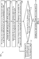
- FIG. 1 is a flow chart 100 for manufacturing a display device.
- the flow chart 100 includes multiple steps 102, 104, 106, 108, 110, 112 and 114. Each of steps may correspond to FIGs. 2A-2G or FIGs. 3A-3D .
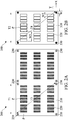
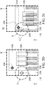
- FIGs. 2A-2G illustrate the steps in the top view.
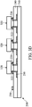
- FIGs. 3A-3D illustrate the steps in the cross-sectional view.
- other steps may be appropriately added before or after above the steps.
- the above partial steps may be appropriately deleted or replaced.
- the above sequence of steps can be changed or modulated as needed.
- the method for manufacturing the display device includes the step 102 of providing an array module having at least one first alignment mark and a light-emitting module having at least one second alignment mark.
- an array module 200 and a light-emitting module 300 are provided.
- the array module 200 includes a first substrate 210.
- the first substrate 210 may include a glass substrate, a ceramic substrate, a plastic substrate or another suitable substrate, but not limited.
- the first substrate 210 may include polyimide (PI), polycarbonate (PC), or polyethylene terephthalate (PET), but not limited thereto.
- the array module 200 includes a plurality of pads 220. The pads 220 are disposed on the first substrate 210.
- the material of the pad 220 may include copper (Cu), aluminum (Al), molybdenum (Mo), gold (Au), chromium (Cr), nickel (Ni), platinum (Pt), titanium (Ti), iridium (Ir), other suitable material, or the above alloy, but is not limited.
- the display device comprises a plurality of pixels P.
- FIG. 2A illustrates a pixel P that may correspond to (or electrically connected to) six pads 220, and a sub-pixel (correspond to one light-emitting element 320) may respectively correspond to two pads 220, but is not limited thereto.
- the dotted line may correspond to a position where the pixel (not shown in FIG.2A ) is expected to be bonded.
- one pixel P may include three sub-pixels, and a sub-pixel may respectively correspond to or electrically connected to two pads 220 after bonding (subsequent step 114 will be described).
- a pixel P may correspond to (or electrically connected to) four pads 220, for example, one of the four pads 220 is a shared pad, the shared pad is electrically connected to three sub-pixels of the pixel P, and other pads may respectively correspond to (or electrically connected to) three sub-pixels with different colors.
- at least part of the pixel P may overlap with corresponding pads 220 in Z direction, and Z direction may defined as a normal direction of the first substrate 210 of the array module 200.
- the array module 200 includes at least one first alignment mark 230 on the first substrate 210.
- the light-emitting module 300 includes a second substrate 310.
- the second substrate 310 may be a carrier substrate or growth substrate, but is not limited.
- the second substrate 310 may include a glass substrate, a ceramic substrate, a plastic substrate, a sapphire substrate or another suitable substrate, but is not limited.
- the growth substrate may include silicon or a sapphire substrate, which includes alumina oxide, GaP, GaAs, AlGaAs, SiC, Si, or another suitable material, but is not limited.
- the light-emitting module 300 includes a plurality of light-emitting elements 320.
- the light-emitting elements 320 may be disposed on the second substrate 310.
- the light-emitting element 320 may be a red sub-pixel, a green sub-pixel or a blue sub-pixel, an infrared (IR) sub-pixel, or other sub-pixel with other colors.
- the light-emitting element 320 may include light-emitting diode (LED), micro LED ( ⁇ LED), mini LED, quantum dot (QD), quantum dot LED (QLED or QDLED) or other suitable element, but is not limited.
- the light-emitting element 320 may emit blue light (or UV light), but is not limited.
- the light-emitting element 320 may respectively emit the light with different colors (such as red, green, blue or other suitable colors).
- the light-emitting module 300 may include the light conversion elements, the light conversion elements (such as quantum dot, but is not limited) may be disposed on or adjacent to the light-emitting module 300.
- the light-emitting module 300 includes at least one second alignment mark 330 on the second substrate 310.
- at least one pixel P may be disposed between two adjacent second alignment marks 330, but not limited, the quantity of pixel P can be adjusted as needed.
- the position of the second alignment mark 330 of the light-emitting module 300 may correspond to the position of the first alignment mark 230 of the array module 200.
- four second alignment marks 330 of the light-emitting module 300 may respectively correspond to one of four first alignment marks 230 on the right part (or on the left part) of the array module 200, but not limited.
- X direction may be defined as a direction parallel to an extension direction of the long side of the first substrate 210, but not limited.
- the X direction may be defined as an arrangement direction of adjacent pixels. In some embodiments, the X direction may be defined as an arrangement direction of sub-pixels of the pixel P. Y direction may be perpendicular with Z direction and X direction.
- First distance T1 may be defined as a distance between a center of one of the first alignment marks 230 and a center of another first alignment mark 230 adjacent to the one of the first alignment marks 230 along the X direction (or Y direction).
- Second distance T2 may be defined as a distance between a center of one of the second alignment marks 330 and a center of another second alignment marks 330 adjacent to the one of the second alignment marks 330 along the X direction(or Y direction).
- the ratio of the first distance T1 to the second distance T2 is in a range from 0.8 to 1.2, but not limited. In some embodiments, the ratio of the first distance T1 to the second distance T2 is in a range from 0.9 to 1.1.
- Distance T3 may be defined as a distance between a center of one of the first alignment marks 230 and a center of another first alignment mark 230 along a direction of the diagonal line.
- Distance T4 may be defined as a distance between a center of one of the second alignment marks 330 and a center of another second alignment marks 330 along a direction of the diagonal line.
- the ratio of distance T3 to distance T4 is in a range from 0.8 to 1.2, but not limited. In some embodiments, the ratio of distance T3 to distance T4 is in a range from 0.9 to 1.1.
- the ratio of distance T3 to distance T4 (or first distance T1 to second distance T2) is in the range mentioned above, the accuracy of bonding the array module 200 and the light-emitting module 300 may be increased.
- the distance between two adjacent first alignment marks 230 along the X direction is the same as or different from the distance between two adjacent first alignment marks 230 along the Y direction. In some embodiments, the distance between two adjacent second alignment marks 330 along the X direction (such as second distance T2) is the same as or different from the distance between two adjacent second alignment marks 330 along the Y direction.
- the second alignment mark 330 has a width W1.
- the light-emitting element 320 has a width W2.
- the width W2 may be a maximum width of one of the light-emitting elements 320 in X direction.
- the width W1 may be a maximum width of one of the second alignment mark 330 in X direction. In some embodiments, the width W1 is less than or equal to the width W2. In some embodiments, the width W1 is greater than the width W2.
- an area of the light-emitting element 320 may be defined as a lighting area of one sub-pixel operating at a highest grayscale in Z direction, but not limited.
- an area of the light-emitting element 320 may defined as a lighting surface (such top surface of the light-emitting element 320) of one sub-pixel, but not limited. In some embodiments, an area of the light-emitting element 320 may be defined by the openings of the light blocking layer 630 (shown in FIG.5 to FIG.6 ). In some embodiments, an area of the second alignment mark 330 is less than an area of one pixel of the display device.
- the method for manufacturing the display device includes the step 104 that aligning the array module 200 and the light-emitting module 300 by the first alignment mark 230 and the second alignment mark 330. As shown in FIG. 2C , the light-emitting module 300 may approach (or be transferred to) the right part (or left part) of the array module 200. In some embodiments, a length of the second alignment mark 330 is greater than a length of the first alignment mark 230. In some embodiments, an area of the second alignment mark 330 is greater than an area of the first alignment mark 230.
- the method for manufacturing the display device includes the step 106 that approaching the at least one second alignment mark 330 with the at least one first alignment mark 230 into a detecting region S.
- the detecting region S may be a region that can be detected by a charge-coupled device (CCD) camera (not shown) or other suitable image equipment (or camera equipment), but not limited.
- CCD charge-coupled device
- the light-emitting module 300 or the array module 200 may be transferred, so that the second alignment mark 330 and the first alignment mark 230 would be inside the detecting region S.
- the method for manufacturing the display device includes the step 108 that detecting the distance between the second alignment mark 330 and the first alignment mark 230, and comparing the distance with a predetermined value.
- FIG. 2E which is an enlarged view of the region R shown in FIG. 2C .
- the distance between the first alignment mark 230 and the second alignment mark 330 is detected by the CCD camera or other suitable image equipment (or camera equipment), but not limited, and the distance between the first alignment mark 230 and the second alignment mark 330 will be compared with the predetermined value.
- the CCD camera or other suitable image equipment or camera equipment
- the pitch between the pixels P is a pixel pitch W3, and the predetermined value is less than or equal to half of the pixel pitch W3.
- the pixel pitch W3 may be a distance between the centers (left sides or right sides) of the two adjacent pixels P, but not limited.
- the pixel pitch P may be a distance between the centers (left sides or right sides) of two adjacent sub-pixels with the same color.
- the method for manufacturing the display device includes the step 110 that determining whether the distance is less than or equal to the predetermined value.
- the step 110 includes determining whether the distance X1 along the X direction (or the distance Y1 along the Y direction) is less than or equal to the predetermined value.
- the distance X1 is the distance between the first alignment mark 230 and the second alignment mark 330 along the X direction
- the distance Y1 is the distance between the first alignment mark 230 and the second alignment mark 330 along the Y direction.
- the step 112 includes reducing the distance between the second alignment mark 330 and the first alignment mark 230.
- the step 112 includes adjusting the position of the array module 200 or the light-emitting module 300, so that the first alignment mark 230 would be aligned with (or overlapped with) the second alignment mark 330.
- the step 112 includes approaching the array module 200 or the light-emitting module 300 along the X direction (or the Y direction or other directions), so that the first alignment mark 230 would be aligned with (or overlapped with) the second alignment mark 330, but not limited.
- the step 108 is performed to detect the distance between the first alignment mark 230 and the second alignment mark 330 along the X direction (or the Y direction or other directions).
- the step 114 includes bonding the light-emitting module 300 onto the array module 200.
- the second substrate 310 may be disposed on the right part (left part or other part) of the first substrate 210, but not limited.
- the light-emitting elements 320 may be electrically connected to the corresponding pad 220. In some embodiments, the light-emitting elements 320 may respectively overlap with part of the corresponding pad 220 in Z direction.
- the predetermined value is less than or equal to half of the pixel pitch W3 of the pixels P. In some embodiments, the predetermined value is equal to the width W2. In some embodiments, when the predetermined value is in the range mentioned above, the production yield of bonding the array module 200 and the light-emitting module 300 may be increased.
- the second substrate 310 may be removed (as shown in FIG. 2G ), and the light-emitting elements 320 are disposed on (or bonded onto) the pad 220.
- the second substrate 310 may be removed by a laser or other suitable methods.
- the second substrate 310 may not be removed, and the second substrate 310 and the light-emitting elements 320 may disposed on the array module 200.
- the process shown in FIGs. 2A-2G may be repeated so that another light-emitting module 300 may be disposed on (or bonded on) the another part (such as left part) of the array module 200.
- the process shown in FIGs. 2A-2G may be used in mass production of the display device, but not limited. For example, nine pixels may be disposed on (or bonded onto) the corresponding pads 220 in same bonding process, but not limited.
- the second substrate 310 may be used as a growth substrate, and the second alignment marks may be disposed on (or formed on) the second substrate 310.
- the second substrate 320 may be used as a carrier substrate, and the light-emitting elements 320 may be transferred onto the second substrate 320, and then transferred onto (or disposed on) the array module 200, but not limited.
- the quantity (number) of first alignment marks 230 may be greater than or equal to the quantity (number) of the second alignment marks 330, but not limited.
- the light-emitting module 300 may have four second alignment marks 330, and the four second alignment marks 330 may respectively be disposed at four corners of the second substrate 310, but not limited.
- the quantity of the second alignment marks 330 in light-emitting module 300 is greater than (or less than) four, and the second alignment marks 330 may be disposed at other suitable position of the second substrate 310.
- the light-emitting module 300 has two second alignment marks 330, and two second alignment marks 330 may respectively be disposed at two diagonal corners of the second substrate 310.
- the light-emitting module 300 may have at least one second alignment mark 330.
- the quantity of the first alignment marks 230 or the position of the first alignment marks 230 may be correspond to the second alignment marks 330, which can be adjusted according to the needs.
- the array module 200 includes a circuit layer 240, and the circuit layer 240 is disposed on (or formed on) the first substrate 210. Furthermore, the circuit layer 240 may include wires 250, other conductive elements (not shown), other dielectric layers (not shown), but not limited. In some embodiments, the pads 220 may be disposed on (or electrically connected to) the circuit layer 240. In some embodiments (shown in fig.3A ), the first alignment mark 230 may be disposed on the circuit layer 240.
- the first alignment mark 230 may be disposed in (or formed in) the circuit layer 240 (not shown in Fig. 3A to Fig. 3D , for example, referring to FIG. 5 , the first alignment mark 522 is disposed in the circuit layer 503).
- the material of the first alignment mark 230 may be the same as or different from the pads 220, the wires 250 or other conductive elements of the circuit layer 240.
- the first alignment mark 230 and the pads 220, the wires 250 or other conductive elements of the circuit layer 240 may be formed in the same process or different process, but not limited.
- the first alignment mark 230 may be formed before the process of forming the circuit layer 240.
- the first alignment mark 230 may be formed after the process of forming the pad 220.
- the material of the first alignment mark 230 may include opaque materials, shading materials, reflective materials or a combination of the above, but is not limited thereto.
- the material of the first alignment mark 230 may include metal material, metal alloy, black photoresist or other suitable material, but is not limited thereto.
- the light-emitting module 300 includes a plurality of pads 322 disposed on the light-emitting element 320.
- the distance D1 may be a distance between a center of the first alignment mark 230 and a center of the second alignment mark 330 along the X direction (or the Y direction). If the distance D1 is greater than the predetermined value, the position of the light-emitting module 300 will be fine-tuned.
- the position of the light-emitting module 300 is fine-tuned.
- the distance D1 is less than or equal to the predetermined value
- the light-emitting module 300 is bonded onto the array module 200 as shown in FIG. 3C .
- the second alignment mark 330 may approximately overlap with the first alignment mark 230 in Z direction, or the second alignment mark 330 may approximately aligned with the first alignment mark 230.
- the second substrate 310 may be removed, but not limited.
- the light-emitting elements 320 and the pads 322 may be disposed on the array module 200.
- the pads 322 of the light-emitting module 300 may electrically connected to (or contact with) the corresponding pads 220 of the array module 200.
- the light-emitting element 320 may be electrically connected to the pad 220 through the pad 322. According to some embodiments, if the distance D1 is less than or equal to the predetermined value, the production yield in mass producing the display device can increase.
- FIGs. 4A and 4B are top views of a first alignment mark and a second alignment mark in accordance with some embodiments.
- the profile of the first alignment marks and second alignment marks shown in FIGs. 4A and 4B are merely examples, and the present disclosure is not limited thereto.
- the first alignment mark 230A and the second alignment mark 330A are in different shapes.
- the second alignment mark 330A may be adjacent to the first alignment mark 230A.
- the second alignment mark 330A may enclose the first alignment mark 230A, as shown in FIG. 4A .
- the second alignment mark may have an opening O, at least part of the opening O may overlap with the first alignment mark 230A in Z direction, but not limited. In some embodiments, at least part of the second alignment mark 330A may overlap with at least part of the first alignment mark 230A in Z direction.
- the shape of the first alignment mark 230A and the shape of the second alignment mark 330A may include rectangle, circle, triangle, polygon, arc shape, obtuse angle shape, acute angle shape, round shape or other suitable shapes, but is not limited. In some embodiments, the shape of the first alignment mark 230A may be the same as or different from the shape of the second alignment mark 330A.
- a distance dm between the second alignment mark 330A and the first alignment mark 230A in X direction (or Y direction) is greater than or equal to 0, and less than or equal to the width W2 (shown in Fig.2B ).
- Distance dm may be defined as the minimum distance between the second alignment mark 330A and the first alignment mark 230A in X direction (or Y direction).
- the position of the first alignment mark 230A and the position of the second alignment mark 330A can be exchanged.
- the second alignment mark 330B may have discontinuous parts, as shown in FIG. 4B .
- the profile of the shape of the second alignment mark 330B is different from or the same as the shape of the first alignment mark 230B.
- the first alignment mark 230B may have a cross-shape, rectangular shape, polygonal shape, curved shape, circular shape, arc shape, obtuse angle shape, acute angle shape, round shape or other suitable shapes, but not limited.
- the first alignment mark 230B may include protruding portions.
- the second alignment mark 330B may be adjacent to the first alignment mark 230B, and the second alignment mark 330B may have any shape correspond to (or in accordance with) the shape of the first alignment mark 230B, but not limited.
- the second alignment mark 330B may have an L-shape (or other shape) and extend into the space between two adjacent protruding portions of the first alignment mark 230B, but not limited.
- the above "the second alignment mark 330B has any shape correspond to (or in accordance with) the shape of the first alignment mark 230B" includes that the second alignment mark 330B has any shape correspond to at least one side of the first alignment mark 230B.
- one of the second alignment marks 330B may have discontinuous parts, these parts may correspond to one of the first alignment marks 230B, these parts can form a second alignment marks 330B, and these parts may have similar or different shapes.
- the position of the first alignment mark 230B and the position of the second alignment mark 330B can be exchanged.
- the shape of the first alignment mark 230B and the shape of the second alignment mark 330B may be complement each other.
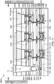
- the display device 400A may include an array module 500 and a light-emitting module 600.
- the array module 500 may include a substrate 502.
- the material of the substrate 502 may be the same as or similar to the material of the first substrate 210.
- some insulating layers 504, 506, 508', 508 may be sequentially disposed on the substrate 502.
- the insulating layers 504, 506, 508 may include, but are not limited to, silicon oxide, silicon nitride, silicon oxynitride or another suitable material.
- a circuit layer 503 is disposed on the substrate 502.
- the circuit layer 503 may include a plurality of transistors 510.
- the transistor 510 may be a thin film transistor (TFT).
- the transistor 510 may include a gate electrode 512, a source/drain electrode 518, and a semiconductor layer 516.
- the gate electrode 512 may be disposed on the insulating layer 504 and the semiconductor layer 516.
- the source/drain electrode 518 may be disposed on the semiconductor layer 516 and the doping layers 514, and the semiconductor layer 516 may be disposed between the doping layers 514.
- the material of the gate electrode 512 and the source/drain electrode 518 may include, but is not limited to, copper (Cu), aluminum (Al), molybdenum (Mo), gold (Au), chromium (Cr), nickel (Ni), titanium (Ti), other suitable material or alloy.
- the material of the semiconductor layer 516 may include, but is not limited to, amorphous silicon, polysilicon such as low-temp polysilicon (LTPS), metal oxide or other suitable materials.
- the metal oxide may include indium gallium zinc oxide (IGZO), indium zinc oxide (IZO), indium gallium zinc tin oxide (IGZTO) or other suitable material.
- the array module 500 may include a plurality of wires 509 and pads 520.
- the pads 520 may be disposed on the circuit layer 503. According to some embodiments, the pads 520 may be disposed on the insulating layer 508 and the wires 509.
- the transistor 510 may be electrically connected to the pad 520 through the wire 509, but not limited.
- the material of the wire 509 and the pad 520 may be the same as or different from the material of the source/drain electrode 518.
- the first alignment mark 522 may be disposed on the insulating layer 504. In some embodiments, the first alignment mark 522 and the gate electrode 512 may be formed in the same process. In some embodiments, the material of the first alignment mark 522 and the material of the gate electrode 512 may be same. In some embodiments, the first alignment mark 522 may include metal material that is disposed in the insulating layer 506. In other embodiments, the first alignment mark 522 and the pad 520 may be formed in the same process. In some embodiments, the material of the first alignment mark 522 and the material of the gate electrode 512 may be same. In other embodiments, the material of the first alignment mark 522 and the material of source/drain electrode 518 may be same.
- the light-emitting module 600 includes a substrate 602.
- the substrate 602 may include a glass substrate, a ceramic substrate, a plastic substrate or another suitable substrate, but not limited.
- the material of the substrate 602 may include sapphire, Si, SiC, other suitable materials or combinations thereof, but are not limited thereto.
- the light-emitting module 600 may include insulating layers 604, 606, 608, and the insulating layers 604, 606, 608 are disposed on the substrate 602.
- the insulating layers 604, 606, 608 may include, but are not limited to, silicon oxide, silicon nitride, silicon oxynitride or another suitable material.
- the light-emitting module 600 may include a plurality of the transistors 610.
- the transistor 610 may include a gate electrode 612, a source/drain electrode 614, and a semiconductor layer 616.
- the gate electrode 612 may be disposed on the insulating layer 604.
- the materials of the gate electrode 612, the source/drain electrode 614 and the semiconductor layer 616 may be the same as, similar to or different from those of the gate electrode 512, the source/drain electrode 518 and the semiconductor layer 516, respectively.
- the light-emitting module 600 includes a plurality of wires 618 and pads 620.
- the transistor 610 may be electrically connected to the pad 620 through the wire 618.
- the transistor 510 may be electrically connected to the transistor 610.
- the pad 520 may be electrically connected to (or contact with) the pad 620.
- the transistor 610 may use as a driving transistor.
- the transistor 510 may use as a switch transistor.
- more transistors (or elements) may be disposed on the substrate 602 or the substrate 502, such as reset transistor or capacitor, but not limited.
- the transistor 610 and the transistor 510 may disposed on the same substrate (such as substrate 602 or the substrate 502).
- the structure of the transistor 610 (or the transistor 510) described above is an example, and the disclosure is not limited thereto.
- the transistor 610 (or the transistor 510) can be top gate thin film transistor, bottom gate thin film transistor, double gate thin film transistor, but not limited.
- the transistor 610 (or the transistor 510) can include amorphous silicon (a-Si:H) transistor, low temperature poly-silicon (LTPS) transistor, indium gallium zinc oxide transistor (IGZO) or other suitable transistor, but not limited.
- the light-emitting element 626 may be electrically connected to the transistor 610 and the transistor 510 through the conductive elements which are disposed in the array module 500 or the light-emitting module 600. According to some embodiments, at least one of the light-emitting elements 626 may be electrically connected to at least one of the pads 520 in the array module 500.
- the light-emitting module 600 includes insulating layer 622 and insulating layer 624.
- the light-emitting module 600 includes a plurality of light-emitting elements 626 and pads 628.
- the light-emitting element 626 and the pad 628 may be surrounded by the insulating layer 622 and the insulating layer 624, but not limited.
- the insulating layer 622 and the insulating layer 624 may be disposed to protect the light-emitting element 626 or the pad 628 from damage or pollution (such as water or air), but not limited.
- the material of the insulating layer 622 (or the insulating layer 624) may include, but is not limited to, resin or another suitable material.
- the light-emitting element 626 and the pad 628 may be the same as or similar to the light-emitting element 320 and the pad 322 shown in FIG. 3A , respectively.
- the order of the above layers or elements can be changed or replaced as needed.
- the above layers can be replaced or removed as needed.
- the light-emitting module 600 includes a light blocking layer 630.
- the light blocking layer 630 may be disposed on the light-emitting element 626.
- the light blocking layer 630 has a plurality of openings B-O, the openings B-O may overlap with the light-emitting element 626 in Z direction. In some embodiments, the light blocking layer 630 does not overlap with the light-emitting element 626 in Z direction.
- the light-emitting module 600 may include a plurality of light conversion layer 632.
- the light conversion layer 632 may be disposed on (or cover) the light-emitting element 626. In some embodiments, the light conversion layer 632 may be adjacent to the light-emitting element 626.
- the material of the light conversion layer 632 may include, but is not limited to, quantum dot, fluorescent material, phosphorescent material or another conversion material.
- the light conversion layer 632 may be an organic or an inorganic layer blended with a quantum dot.
- the quantum dot may include, but is not limited to, zinc, cadmium, selenium, sulfur, InP, GaSb, GaAs, CdSe, CdS, ZnS or a combination thereof.
- the light-emitting module 600 further includes a protective layer 634 and a color filter layer 636.
- the light-emitting element 626 may be disposed between the protective layer 634 and the substrate 602.
- the color filter layer 636 may be disposed between the light conversion layer 632 and the protective layer 634, but not limited.
- the protective layer 634 may be single layer structure, multilayer structure, composite structure, but not limited.
- the material of the protective layer 634 may include organic material, inorganic material, or a combination thereof. In some embodiments, the material of the protective layer 634 may be a transparent substrate.
- the material of the protective layer 634 may include phosphosilicate glass (PSG), borophosphosilicate glass (BPSG), silicon oxide, silicon nitride, or silicon oxynitride, but not limited.
- the color filter layer 636 may be disposed on at least one of the light conversion layer 632. In some embodiments, the color filter layer 636 may be respectively disposed on the corresponding light conversion layer 632. In some embodiments, the color filter layer 636 may overlap with at least part of the light blocking layer 630 in Z direction in order to reduce light leakage. In some embodiments (not shown), the color filter layer 636 may disposed between the light conversion layer 632 and the light-emitting element 626.
- the second alignment mark 638 may be disposed in (or formed in) the second substrate 602.
- the second substrate 602 may be a transparent substrate or non-transparent substrate
- a through hole TH may penetrate the second substrate 602
- the through hole TH may be regarded as the second alignment mark 638.
- the through hole TH may penetrate at least part of the layers (or the elements) formed on the substrate 602.
- the through hole TH may penetrate the substrate 602, the insulating layers 604, 606, 608, 622, 624, the light blocking layer 630 and the protective layer 634, but not limited.
- a shape of the through hole TH may include rectangle, circle, triangle, polygon, arc shape, obtuse angle shape, acute angle shape, round shape or other suitable shapes, but not limited.
- the through hole in the direction of the cross section, has an inverted trapezoid profile, rectangular profile or other shape profile, but not limited.
- the scope of the disclosure is not limiting.
- the second alignment mark 638 approximately overlap with (or aligned with) the first alignment mark 522 in Z direction.
- the second alignment mark 638 (such as through hole TH) have a bottom surface BS and top surface TS opposite to the bottom surface BS, and the bottom surface BS is near to the array module 500.
- the bottom surface BS of the second alignment mark 638 (such as through hole TH) may have a length L1
- the top surface TS of the second alignment mark 638 may have length L3.
- the length L3 may be greater than or equal to the length L1.
- the length L3 may be less than or equal to the length L1.
- the length L3 also may be defined as the maximum length of the top surface TS of the second alignment mark 638 in top view
- length L1 also may be defined as the maximum length of the bottom surface BS of the second alignment mark 638 in top view.
- the first alignment mark 522 has a length L2.
- the length L1 is greater than or equal to the length L2.
- the length L1 is greater than the length L2 so that the CCD camera could receive both images of the first alignment mark 522 and the second alignment mark 638.
- the angle ⁇ may be in a range from about 30° to about 110°, but not limited. In some embodiments, the angle ⁇ is in a range from about 50° to about 90°.
- the angle ⁇ is in a range from about 70° to about 90°.
- the side surface of the second alignment mark 638(such as through hole TH) is a curved edge or an irregular edge. For example, in the Z direction, viewers can see the elements (such as first alignment mark 522 or other layers (or elements) of the array module 500) through the second alignment mark 638 (through hole TH).
- At least one spacer 524 may be disposed between the array module 500 and the light-emitting module 600.
- the spacer 524 may include resin or other suitable materials, but not limited.
- at least one space 526 may be formed between the array module 500 and the light-emitting module 600 by the spacer 524.
- the space 526 may include air, transparent material or other suitable materials, but not limited.
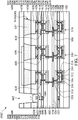
- a second alignment mark 640 of the display device 400B may include a filling materials FM
- the filling materials FM may be disposed in (or filled in) the through hole TH
- the through hole TH with the filling materials FM may be regarded as the second alignment mark 330.
- the filling materials may include transparent material.
- the filling materials FM may include, but is not limited to, silicon oxide, silicon nitride, silicon oxynitride or another suitable material.
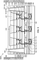
- FIG. 7 illustrates a cross-sectional view of a display device 400C in accordance with some embodiments.
- a notch 642 may penetrate part of layers (or elements) in the light-emitting module 600.
- the notch 642 may penetrate the insulating layers 622, 624, the light blocking layer 630 and the protective layer 634.
- the display device 400C may include a second alignment mark 644.
- the material of the second alignment mark 644 may be the same as or similar to the material of the gate electrode 612 of the transistor 610, but not limited.
- the second alignment mark 644 and a portion of the transistor 610 may be formed in the same process or different process.
- the material of the second alignment mark 644 may be the same as or different from the material of a portion of the transistor 610 (such as source/drain electrode 614).
- the notch 642 has a bottom surface BS', and the bottom surface BS' is near to the array module 500.
- the bottom surface BS' of the notch 642 may have a length L1'.
- the length L1' may be defined as the maximum length of the bottom surface BS' of the notch 642 in top view.
- the second alignment mark 644 has length L4, the length L4 may be defined as the maximum length of the second alignment mark 644 in X direction (or Y direction). In some embodiments, the length L4 is less than or equal to the length L1'.
- at least part of the second alignment mark 644 may overlap with the first alignment mark 522 in Z direction. In some embodiments, at least part of the second alignment mark 644 may be aligned with the first alignment mark 522.
- the shape of the notch 642 may be the same as or different from of shape of the second alignment mark 644 in Z direction.
- the array module 500 of the display device 400D may include a spacer 528 and a protruding portion 530 that is disposed on the spacer 528.
- the protruding portion 530 may be regarded as the first alignment mark of the array module 500.
- the profile of a second alignment mark 646 of the light-emitting module 600 may be correspond to (or accordance with) the profile of the protruding portion 530.
- the protruding portion 530 may protrude into the second alignment mark 646 of the light-emitting module 600.
- the display device 400 may include a plurality of solders 532 that are electrically connected to the pads 520 and the pads 620.
- at least one space 534 may be formed between the array module 500 and the light-emitting module 600 by the spacer 528.
- the space 534 may include air, a transparent material, or other suitable materials, but the disclosure is not limited thereto.
- a display device 700 may include two or more light-emitting modules with different arrangements.
- the display device 700 may include an active region 710 and a peripheral region 720 that is adjacent to (or surrounds) the active region 710.
- the display device 700 may include a plurality of second alignment marks 830A and 830B on the peripheral region 720 and the active region 710.
- the second alignment marks 830A are located on the peripheral region 720
- the second alignment marks 830B are located on the active region 710.
- a light-emitting module 800A may have a second substrate 810, light-emitting elements 820 and second alignment marks 830A.
- FIG. 9A a light-emitting module 800A may have a second substrate 810, light-emitting elements 820 and second alignment marks 830A.
- a light-emitting module 800B may have a second substrate 810, light-emitting elements 820 and second alignment marks 830B.
- One of the differences between the light-emitting module 800A and the light-emitting module 800B is the arrangement of the light-emitting elements 820.
- the display device 700 may include a plurality of second alignment marks 830A of the light-emitting module 800A and a plurality of second alignment marks 830B of the light-emitting module 800B.
- the arrangement of the light-emitting module 800A and the light-emitting module 800B may be adjusted according to the active region 710 and the peripheral region 720.
- the second alignment mark 830A may be disposed on the active region 710 and the peripheral region 720.
- the second alignment mark 830B may be disposed on the active region 710.
Landscapes
- Engineering & Computer Science (AREA)
- Manufacturing & Machinery (AREA)
- Led Device Packages (AREA)
- Electroluminescent Light Sources (AREA)
Applications Claiming Priority (1)
| Application Number | Priority Date | Filing Date | Title |
|---|---|---|---|
| US16/242,228 US11018089B2 (en) | 2019-01-08 | 2019-01-08 | Display devices and methods for manufacturing the same |
Publications (2)
| Publication Number | Publication Date |
|---|---|
| EP3680933A1 true EP3680933A1 (fr) | 2020-07-15 |
| EP3680933B1 EP3680933B1 (fr) | 2025-05-28 |
Family
ID=69055841
Family Applications (1)
| Application Number | Title | Priority Date | Filing Date |
|---|---|---|---|
| EP19220015.2A Active EP3680933B1 (fr) | 2019-01-08 | 2019-12-30 | Dispositif d'affichage et procédé de fabrication associé |
Country Status (4)
| Country | Link |
|---|---|
| US (3) | US11018089B2 (fr) |
| EP (1) | EP3680933B1 (fr) |
| KR (1) | KR102998948B1 (fr) |
| CN (1) | CN111415955A (fr) |
Cited By (1)
| Publication number | Priority date | Publication date | Assignee | Title |
|---|---|---|---|---|
| WO2022026539A1 (fr) * | 2020-07-29 | 2022-02-03 | Lumileds Llc | Alignement d'élément d'éclairage |
Families Citing this family (23)
| Publication number | Priority date | Publication date | Assignee | Title |
|---|---|---|---|---|
| US11239399B2 (en) * | 2019-02-05 | 2022-02-01 | Facebook Technologies, Llc | Architecture for hybrid TFT-based micro display projector |
| US20220157854A1 (en) * | 2019-02-26 | 2022-05-19 | Kyocera Corporation | Micro-light-emitting diode mounting board and display device including micro-light-emitting diode mounting board |
| KR102657174B1 (ko) * | 2019-04-08 | 2024-04-15 | 삼성디스플레이 주식회사 | 전자 패널 및 이의 제조 방법 |
| US11088306B2 (en) * | 2019-04-08 | 2021-08-10 | Innolux Corporation | Light-emitting devices and methods for manufacturing the same |
| CN110634839B (zh) * | 2019-09-26 | 2021-11-26 | 京东方科技集团股份有限公司 | 微发光二极管显示基板、装置及制备方法 |
| US11362038B2 (en) * | 2020-05-28 | 2022-06-14 | Taiwan Semiconductor Manufacturing Company, Ltd. | Photolithography alignment process for bonded wafers |
| DE102020126211A1 (de) | 2020-05-28 | 2021-12-02 | Taiwan Semiconductor Manufacturing Co. Ltd. | Photolithographie-Ausrichtungsprozess für gebondete Wafer |
| CN111627952B (zh) * | 2020-06-19 | 2022-04-08 | 武汉华星光电技术有限公司 | 显示面板及其制备方法、显示装置 |
| CN112164334B (zh) * | 2020-10-27 | 2022-08-26 | 湖北长江新型显示产业创新中心有限公司 | 显示面板、显示装置及显示面板的制备方法 |
| KR102987729B1 (ko) * | 2020-11-24 | 2026-07-07 | 삼성디스플레이 주식회사 | 표시 장치의 제조 장치와 제조 방법 |
| CN115148881A (zh) | 2021-03-31 | 2022-10-04 | 群创光电股份有限公司 | 制作显示装置的方法 |
| CN113380865B (zh) * | 2021-06-07 | 2024-11-08 | 京东方科技集团股份有限公司 | 显示装置 |
| US12564067B2 (en) * | 2021-09-01 | 2026-02-24 | Micron Technology, Inc. | Wafer alignment for stacked wafers and semiconductor device assemblies |
| WO2023123270A1 (fr) * | 2021-12-30 | 2023-07-06 | 厦门市芯颖显示科技有限公司 | Panneau d'affichage, appareil d'affichage et procédé de fabrication d'un panneau d'affichage |
| CN114512471A (zh) * | 2022-01-10 | 2022-05-17 | 深圳市思坦科技有限公司 | 一种发光装置及判定芯片焊接偏移方法 |
| CN116723724A (zh) * | 2022-02-28 | 2023-09-08 | 群创光电股份有限公司 | 电子装置 |
| US12125800B2 (en) | 2022-03-01 | 2024-10-22 | Nanya Technology Corporation | Semiconductor device structure including overlay mark structure |
| TWI799272B (zh) * | 2022-03-01 | 2023-04-11 | 南亞科技股份有限公司 | 具有疊置標記結構之半導體元件結構的製備方法 |
| US12369439B2 (en) | 2022-03-01 | 2025-07-22 | Nanya Technology Corporation | Method for manufacturing semiconductor device structure including an overlay mark structure |
| CN115274528B (zh) * | 2022-09-22 | 2022-12-06 | 西北电子装备技术研究所(中国电子科技集团公司第二研究所) | 一种芯片倒装键合用标定玻璃片 |
| KR20250034249A (ko) * | 2023-09-01 | 2025-03-11 | 삼성전자주식회사 | 디스플레이 패널 및 그 제조 방법 |
| US20250087592A1 (en) * | 2023-09-11 | 2025-03-13 | Taiwan Semiconductor Manufacturing Company, Ltd. | Package structure and method for forming the same |
| US20250132265A1 (en) * | 2023-10-18 | 2025-04-24 | Micron Technology, Inc. | Alignment markers for wafer bonding and associated systems and methods |
Citations (2)
| Publication number | Priority date | Publication date | Assignee | Title |
|---|---|---|---|---|
| US20180190672A1 (en) * | 2017-01-03 | 2018-07-05 | Innolux Corporation | Display device |
| KR101902566B1 (ko) * | 2017-07-25 | 2018-09-28 | 엘지디스플레이 주식회사 | 발광 표시 장치 및 이의 제조 방법 |
Family Cites Families (20)
| Publication number | Priority date | Publication date | Assignee | Title |
|---|---|---|---|---|
| JP4701537B2 (ja) * | 2001-05-16 | 2011-06-15 | ソニー株式会社 | 素子の転写方法及び画像表示装置の製造方法 |
| US6838689B1 (en) * | 2002-02-14 | 2005-01-04 | Finisar Corporation | Backside alignment and packaging of opto-electronic devices |
| KR100567911B1 (ko) | 2004-11-23 | 2006-04-05 | 매그나칩 반도체 유한회사 | 웨이퍼 얼라인 방법 |
| JP5906396B2 (ja) | 2011-03-24 | 2016-04-20 | パナソニックIpマネジメント株式会社 | フレキシブル半導体装置及びその製造方法 |
| KR102173801B1 (ko) * | 2012-07-12 | 2020-11-04 | 가부시키가이샤 한도오따이 에네루기 켄큐쇼 | 표시 장치, 및 표시 장치의 제작 방법 |
| DE102012112530A1 (de) * | 2012-12-18 | 2014-06-18 | Osram Opto Semiconductors Gmbh | Verfahren zum Herstellen von optoelektronischen Halbleiterchips und optoelektronischer Halbleiterchip |
| WO2015000095A1 (fr) * | 2013-07-05 | 2015-01-08 | Industrial Technology Research Institute | Écran souple et son procédé de fabrication |
| US9799719B2 (en) | 2014-09-25 | 2017-10-24 | X-Celeprint Limited | Active-matrix touchscreen |
| US9478583B2 (en) * | 2014-12-08 | 2016-10-25 | Apple Inc. | Wearable display having an array of LEDs on a conformable silicon substrate |
| CN104576964A (zh) * | 2014-12-17 | 2015-04-29 | 深圳市华星光电技术有限公司 | 透明柔性封装衬底及柔性oled封装方法 |
| TWI557831B (zh) * | 2015-05-15 | 2016-11-11 | 友達光電股份有限公司 | 微組件的傳送方法 |
| KR102541451B1 (ko) * | 2016-01-08 | 2023-06-09 | 삼성디스플레이 주식회사 | 디스플레이 장치 및 그 제조방법 |
| KR102524805B1 (ko) | 2016-02-12 | 2023-04-25 | 삼성전자주식회사 | 광원 모듈, 디스플레이 패널 및 이를 구비한 디스플레이 장치 |
| KR102480220B1 (ko) | 2016-04-08 | 2022-12-26 | 삼성전자주식회사 | 발광 다이오드 모듈 및 이를 구비한 디스플레이 패널 |
| CN107768498B (zh) * | 2016-08-19 | 2019-07-30 | 群创光电股份有限公司 | 发光二极管显示装置及其制作方法 |
| CN108573991B (zh) * | 2017-03-12 | 2021-10-08 | 美科米尚技术有限公司 | 显示装置的制造方法 |
| JP6823717B2 (ja) * | 2017-05-26 | 2021-02-03 | シャープ株式会社 | 半導体モジュールおよびその製造方法 |
| KR102481818B1 (ko) * | 2017-08-22 | 2022-12-28 | 삼성디스플레이 주식회사 | 전자 부품 및 이를 포함하는 전자 장치 |
| CN108039415B (zh) * | 2017-11-02 | 2019-06-07 | 厦门市三安光电科技有限公司 | 微元件的封装方法 |
| KR102538411B1 (ko) * | 2018-07-25 | 2023-05-31 | 삼성디스플레이 주식회사 | 표시 장치 |
-
2019
- 2019-01-08 US US16/242,228 patent/US11018089B2/en active Active
- 2019-12-04 KR KR1020190159838A patent/KR102998948B1/ko active Active
- 2019-12-30 EP EP19220015.2A patent/EP3680933B1/fr active Active
-
2020
- 2020-01-02 CN CN202010000737.9A patent/CN111415955A/zh active Pending
-
2021
- 2021-04-22 US US17/237,154 patent/US20210242135A1/en not_active Abandoned
-
2024
- 2024-11-14 US US18/947,320 patent/US20250070041A1/en active Pending
Patent Citations (3)
| Publication number | Priority date | Publication date | Assignee | Title |
|---|---|---|---|---|
| US20180190672A1 (en) * | 2017-01-03 | 2018-07-05 | Innolux Corporation | Display device |
| KR101902566B1 (ko) * | 2017-07-25 | 2018-09-28 | 엘지디스플레이 주식회사 | 발광 표시 장치 및 이의 제조 방법 |
| US20190035817A1 (en) * | 2017-07-25 | 2019-01-31 | Lg Display Co., Ltd. | Light emitting display device and method of manufacturing the same |
Cited By (3)
| Publication number | Priority date | Publication date | Assignee | Title |
|---|---|---|---|---|
| WO2022026539A1 (fr) * | 2020-07-29 | 2022-02-03 | Lumileds Llc | Alignement d'élément d'éclairage |
| US12408482B2 (en) | 2020-07-29 | 2025-09-02 | Lumileds Llc | Lighting element alignment |
| EP3958308A1 (fr) * | 2020-08-19 | 2022-02-23 | Lumileds LLC | Alignement d'élément d'éclairage |
Also Published As
| Publication number | Publication date |
|---|---|
| KR102998948B1 (ko) | 2026-07-31 |
| US11018089B2 (en) | 2021-05-25 |
| EP3680933B1 (fr) | 2025-05-28 |
| US20210242135A1 (en) | 2021-08-05 |
| US20250070041A1 (en) | 2025-02-27 |
| US20200219820A1 (en) | 2020-07-09 |
| KR20200086617A (ko) | 2020-07-17 |
| CN111415955A (zh) | 2020-07-14 |
Similar Documents
| Publication | Publication Date | Title |
|---|---|---|
| EP3680933B1 (fr) | Dispositif d'affichage et procédé de fabrication associé | |
| EP3343611B1 (fr) | Dispositif d'affichage | |
| US12040425B2 (en) | Self-aligned display appartus | |
| US11749709B2 (en) | Display device | |
| US11824138B2 (en) | Display device and method of fabricating the same | |
| CN107393940B (zh) | Led显示设备及其制造方法 | |
| TWI811680B (zh) | 發光二極體微型顯示裝置 | |
| KR102771958B1 (ko) | 표시 장치 및 이를 포함하는 타일형 표시 장치 | |
| US10879218B2 (en) | Display device and method of manufacturing the same | |
| TWI663744B (zh) | 發光二極體顯示器 | |
| US12336333B2 (en) | Display device | |
| KR102811766B1 (ko) | 표시 장치 | |
| KR102951201B1 (ko) | 표시 장치 및 표시 장치 제조 방법 | |
| WO2020203702A1 (fr) | Dispositif d'affichage | |
| US12575462B2 (en) | Display device and fabrication method thereof | |
| US20240222589A1 (en) | Light-emitting module, method for sorting the same, and display device | |
| US12550501B2 (en) | Display device | |
| US20240014363A1 (en) | Display device | |
| US20240224750A1 (en) | Display panel and display device | |
| KR20200081223A (ko) | 표시 장치 | |
| KR100768238B1 (ko) | 노치필터를 구비한 유기발광소자 |
Legal Events
| Date | Code | Title | Description |
|---|---|---|---|
| PUAI | Public reference made under article 153(3) epc to a published international application that has entered the european phase |
Free format text: ORIGINAL CODE: 0009012 |
|
| STAA | Information on the status of an ep patent application or granted ep patent |
Free format text: STATUS: THE APPLICATION HAS BEEN PUBLISHED |
|
| AK | Designated contracting states |
Kind code of ref document: A1 Designated state(s): AL AT BE BG CH CY CZ DE DK EE ES FI FR GB GR HR HU IE IS IT LI LT LU LV MC MK MT NL NO PL PT RO RS SE SI SK SM TR |
|
| AX | Request for extension of the european patent |
Extension state: BA ME |
|
| STAA | Information on the status of an ep patent application or granted ep patent |
Free format text: STATUS: REQUEST FOR EXAMINATION WAS MADE |
|
| 17P | Request for examination filed |
Effective date: 20210114 |
|
| RBV | Designated contracting states (corrected) |
Designated state(s): AL AT BE BG CH CY CZ DE DK EE ES FI FR GB GR HR HU IE IS IT LI LT LU LV MC MK MT NL NO PL PT RO RS SE SI SK SM TR |
|
| STAA | Information on the status of an ep patent application or granted ep patent |
Free format text: STATUS: EXAMINATION IS IN PROGRESS |
|
| 17Q | First examination report despatched |
Effective date: 20210401 |
|
| GRAP | Despatch of communication of intention to grant a patent |
Free format text: ORIGINAL CODE: EPIDOSNIGR1 |
|
| STAA | Information on the status of an ep patent application or granted ep patent |
Free format text: STATUS: GRANT OF PATENT IS INTENDED |
|
| RIC1 | Information provided on ipc code assigned before grant |
Ipc: H01L 33/62 20100101ALN20241025BHEP Ipc: H01L 23/00 20060101ALI20241025BHEP Ipc: H01L 23/544 20060101ALI20241025BHEP Ipc: H01L 21/683 20060101ALI20241025BHEP Ipc: H01L 25/075 20060101AFI20241025BHEP |
|
| INTG | Intention to grant announced |
Effective date: 20241204 |
|
| RIN1 | Information on inventor provided before grant (corrected) |
Inventor name: WU, YUAN-LIN Inventor name: LEE, KUAN-FENG Inventor name: TSAI, TSUNG-HAN Inventor name: CHEN, JIA-YUAN |
|
| GRAS | Grant fee paid |
Free format text: ORIGINAL CODE: EPIDOSNIGR3 |
|
| GRAA | (expected) grant |
Free format text: ORIGINAL CODE: 0009210 |
|
| STAA | Information on the status of an ep patent application or granted ep patent |
Free format text: STATUS: THE PATENT HAS BEEN GRANTED |
|
| AK | Designated contracting states |
Kind code of ref document: B1 Designated state(s): AL AT BE BG CH CY CZ DE DK EE ES FI FR GB GR HR HU IE IS IT LI LT LU LV MC MK MT NL NO PL PT RO RS SE SI SK SM TR |
|
| REG | Reference to a national code |
Ref country code: GB Ref legal event code: FG4D |
|
| REG | Reference to a national code |
Ref country code: CH Ref legal event code: EP |
|
| REG | Reference to a national code |
Ref country code: DE Ref legal event code: R096 Ref document number: 602019070502 Country of ref document: DE |
|
| REG | Reference to a national code |
Ref country code: IE Ref legal event code: FG4D |
|
| REG | Reference to a national code |
Ref country code: NL Ref legal event code: MP Effective date: 20250528 |
|
| PG25 | Lapsed in a contracting state [announced via postgrant information from national office to epo] |
Ref country code: ES Free format text: LAPSE BECAUSE OF FAILURE TO SUBMIT A TRANSLATION OF THE DESCRIPTION OR TO PAY THE FEE WITHIN THE PRESCRIBED TIME-LIMIT Effective date: 20250528 Ref country code: FI Free format text: LAPSE BECAUSE OF FAILURE TO SUBMIT A TRANSLATION OF THE DESCRIPTION OR TO PAY THE FEE WITHIN THE PRESCRIBED TIME-LIMIT Effective date: 20250528 |
|
| REG | Reference to a national code |
Ref country code: LT Ref legal event code: MG9D |
|
| PG25 | Lapsed in a contracting state [announced via postgrant information from national office to epo] |
Ref country code: GR Free format text: LAPSE BECAUSE OF FAILURE TO SUBMIT A TRANSLATION OF THE DESCRIPTION OR TO PAY THE FEE WITHIN THE PRESCRIBED TIME-LIMIT Effective date: 20250829 Ref country code: NO Free format text: LAPSE BECAUSE OF FAILURE TO SUBMIT A TRANSLATION OF THE DESCRIPTION OR TO PAY THE FEE WITHIN THE PRESCRIBED TIME-LIMIT Effective date: 20250828 |
|
| PG25 | Lapsed in a contracting state [announced via postgrant information from national office to epo] |
Ref country code: PL Free format text: LAPSE BECAUSE OF FAILURE TO SUBMIT A TRANSLATION OF THE DESCRIPTION OR TO PAY THE FEE WITHIN THE PRESCRIBED TIME-LIMIT Effective date: 20250528 Ref country code: NL Free format text: LAPSE BECAUSE OF FAILURE TO SUBMIT A TRANSLATION OF THE DESCRIPTION OR TO PAY THE FEE WITHIN THE PRESCRIBED TIME-LIMIT Effective date: 20250528 |
|
| PG25 | Lapsed in a contracting state [announced via postgrant information from national office to epo] |
Ref country code: BG Free format text: LAPSE BECAUSE OF FAILURE TO SUBMIT A TRANSLATION OF THE DESCRIPTION OR TO PAY THE FEE WITHIN THE PRESCRIBED TIME-LIMIT Effective date: 20250528 |
|
| PG25 | Lapsed in a contracting state [announced via postgrant information from national office to epo] |
Ref country code: HR Free format text: LAPSE BECAUSE OF FAILURE TO SUBMIT A TRANSLATION OF THE DESCRIPTION OR TO PAY THE FEE WITHIN THE PRESCRIBED TIME-LIMIT Effective date: 20250528 |
|
| PG25 | Lapsed in a contracting state [announced via postgrant information from national office to epo] |
Ref country code: RS Free format text: LAPSE BECAUSE OF FAILURE TO SUBMIT A TRANSLATION OF THE DESCRIPTION OR TO PAY THE FEE WITHIN THE PRESCRIBED TIME-LIMIT Effective date: 20250828 |
|
| PG25 | Lapsed in a contracting state [announced via postgrant information from national office to epo] |
Ref country code: IS Free format text: LAPSE BECAUSE OF FAILURE TO SUBMIT A TRANSLATION OF THE DESCRIPTION OR TO PAY THE FEE WITHIN THE PRESCRIBED TIME-LIMIT Effective date: 20250928 |
|
| PG25 | Lapsed in a contracting state [announced via postgrant information from national office to epo] |
Ref country code: LV Free format text: LAPSE BECAUSE OF FAILURE TO SUBMIT A TRANSLATION OF THE DESCRIPTION OR TO PAY THE FEE WITHIN THE PRESCRIBED TIME-LIMIT Effective date: 20250528 |
|
| REG | Reference to a national code |
Ref country code: DE Ref legal event code: R079 Ref document number: 602019070502 Country of ref document: DE Free format text: PREVIOUS MAIN CLASS: H01L0025075000 Ipc: H10H0029240000 |
|
| REG | Reference to a national code |
Ref country code: AT Ref legal event code: MK05 Ref document number: 1799151 Country of ref document: AT Kind code of ref document: T Effective date: 20250528 |
|
| PGFP | Annual fee paid to national office [announced via postgrant information from national office to epo] |
Ref country code: DE Payment date: 20251119 Year of fee payment: 7 |
|
| PGFP | Annual fee paid to national office [announced via postgrant information from national office to epo] |
Ref country code: GB Payment date: 20251120 Year of fee payment: 7 |
|
| PG25 | Lapsed in a contracting state [announced via postgrant information from national office to epo] |
Ref country code: SM Free format text: LAPSE BECAUSE OF FAILURE TO SUBMIT A TRANSLATION OF THE DESCRIPTION OR TO PAY THE FEE WITHIN THE PRESCRIBED TIME-LIMIT Effective date: 20250528 Ref country code: AT Free format text: LAPSE BECAUSE OF FAILURE TO SUBMIT A TRANSLATION OF THE DESCRIPTION OR TO PAY THE FEE WITHIN THE PRESCRIBED TIME-LIMIT Effective date: 20250528 Ref country code: DK Free format text: LAPSE BECAUSE OF FAILURE TO SUBMIT A TRANSLATION OF THE DESCRIPTION OR TO PAY THE FEE WITHIN THE PRESCRIBED TIME-LIMIT Effective date: 20250528 |
|
| PGFP | Annual fee paid to national office [announced via postgrant information from national office to epo] |
Ref country code: FR Payment date: 20251124 Year of fee payment: 7 |
|
| PG25 | Lapsed in a contracting state [announced via postgrant information from national office to epo] |
Ref country code: CZ Free format text: LAPSE BECAUSE OF FAILURE TO SUBMIT A TRANSLATION OF THE DESCRIPTION OR TO PAY THE FEE WITHIN THE PRESCRIBED TIME-LIMIT Effective date: 20250528 |
|
| PG25 | Lapsed in a contracting state [announced via postgrant information from national office to epo] |
Ref country code: EE Free format text: LAPSE BECAUSE OF FAILURE TO SUBMIT A TRANSLATION OF THE DESCRIPTION OR TO PAY THE FEE WITHIN THE PRESCRIBED TIME-LIMIT Effective date: 20250528 |
|
| PG25 | Lapsed in a contracting state [announced via postgrant information from national office to epo] |
Ref country code: RO Free format text: LAPSE BECAUSE OF FAILURE TO SUBMIT A TRANSLATION OF THE DESCRIPTION OR TO PAY THE FEE WITHIN THE PRESCRIBED TIME-LIMIT Effective date: 20250528 Ref country code: SK Free format text: LAPSE BECAUSE OF FAILURE TO SUBMIT A TRANSLATION OF THE DESCRIPTION OR TO PAY THE FEE WITHIN THE PRESCRIBED TIME-LIMIT Effective date: 20250528 |
|
| PG25 | Lapsed in a contracting state [announced via postgrant information from national office to epo] |
Ref country code: IT Free format text: LAPSE BECAUSE OF FAILURE TO SUBMIT A TRANSLATION OF THE DESCRIPTION OR TO PAY THE FEE WITHIN THE PRESCRIBED TIME-LIMIT Effective date: 20250528 |
|
| REG | Reference to a national code |
Ref country code: DE Ref legal event code: R097 Ref document number: 602019070502 Country of ref document: DE |
|
| PLBE | No opposition filed within time limit |
Free format text: ORIGINAL CODE: 0009261 |
|
| STAA | Information on the status of an ep patent application or granted ep patent |
Free format text: STATUS: NO OPPOSITION FILED WITHIN TIME LIMIT |
|
| REG | Reference to a national code |
Ref country code: CH Ref legal event code: L10 Free format text: ST27 STATUS EVENT CODE: U-0-0-L10-L00 (AS PROVIDED BY THE NATIONAL OFFICE) Effective date: 20260409 |
|
| 26N | No opposition filed |
Effective date: 20260303 |
|
| PG25 | Lapsed in a contracting state [announced via postgrant information from national office to epo] |
Ref country code: LT Free format text: LAPSE BECAUSE OF FAILURE TO SUBMIT A TRANSLATION OF THE DESCRIPTION OR TO PAY THE FEE WITHIN THE PRESCRIBED TIME-LIMIT Effective date: 20250528 |
|
| PG25 | Lapsed in a contracting state [announced via postgrant information from national office to epo] |
Ref country code: PT Free format text: LAPSE BECAUSE OF NON-PAYMENT OF DUE FEES Effective date: 20250528 Ref country code: MC Free format text: LAPSE BECAUSE OF FAILURE TO SUBMIT A TRANSLATION OF THE DESCRIPTION OR TO PAY THE FEE WITHIN THE PRESCRIBED TIME-LIMIT Effective date: 20250528 |
|
| REG | Reference to a national code |
Ref country code: CH Ref legal event code: H13 Free format text: ST27 STATUS EVENT CODE: U-0-0-H10-H13 (AS PROVIDED BY THE NATIONAL OFFICE) Effective date: 20260723 |
|
| PG25 | Lapsed in a contracting state [announced via postgrant information from national office to epo] |
Ref country code: SE Free format text: LAPSE BECAUSE OF FAILURE TO SUBMIT A TRANSLATION OF THE DESCRIPTION OR TO PAY THE FEE WITHIN THE PRESCRIBED TIME-LIMIT Effective date: 20250528 |