EP3683948A1 - Stromumwandlungsvorrichtung und stromumwandlungssystem - Google Patents
Stromumwandlungsvorrichtung und stromumwandlungssystem Download PDFInfo
- Publication number
- EP3683948A1 EP3683948A1 EP17924487.6A EP17924487A EP3683948A1 EP 3683948 A1 EP3683948 A1 EP 3683948A1 EP 17924487 A EP17924487 A EP 17924487A EP 3683948 A1 EP3683948 A1 EP 3683948A1
- Authority
- EP
- European Patent Office
- Prior art keywords
- power converter
- power
- control device
- voltage
- terminal
- Prior art date
- Legal status (The legal status is an assumption and is not a legal conclusion. Google has not performed a legal analysis and makes no representation as to the accuracy of the status listed.)
- Granted
Links
Images


Classifications
-
- H—ELECTRICITY
- H02—GENERATION; CONVERSION OR DISTRIBUTION OF ELECTRIC POWER
- H02M—APPARATUS FOR CONVERSION BETWEEN AC AND AC, BETWEEN AC AND DC, OR BETWEEN DC AND DC, AND FOR USE WITH MAINS OR SIMILAR POWER SUPPLY SYSTEMS; CONVERSION OF DC OR AC INPUT POWER INTO SURGE OUTPUT POWER; CONTROL OR REGULATION THEREOF
- H02M1/00—Details of apparatus for conversion
- H02M1/36—Means for starting or stopping converters
-
- H—ELECTRICITY
- H02—GENERATION; CONVERSION OR DISTRIBUTION OF ELECTRIC POWER
- H02M—APPARATUS FOR CONVERSION BETWEEN AC AND AC, BETWEEN AC AND DC, OR BETWEEN DC AND DC, AND FOR USE WITH MAINS OR SIMILAR POWER SUPPLY SYSTEMS; CONVERSION OF DC OR AC INPUT POWER INTO SURGE OUTPUT POWER; CONTROL OR REGULATION THEREOF
- H02M5/00—Conversion of AC power input into AC power output, e.g. for change of voltage, for change of frequency, for change of number of phases
- H02M5/40—Conversion of AC power input into AC power output, e.g. for change of voltage, for change of frequency, for change of number of phases with intermediate conversion into DC
- H02M5/42—Conversion of AC power input into AC power output, e.g. for change of voltage, for change of frequency, for change of number of phases with intermediate conversion into DC by static converters
- H02M5/44—Conversion of AC power input into AC power output, e.g. for change of voltage, for change of frequency, for change of number of phases with intermediate conversion into DC by static converters using discharge tubes or semiconductor devices to convert the intermediate DC into AC
- H02M5/453—Conversion of AC power input into AC power output, e.g. for change of voltage, for change of frequency, for change of number of phases with intermediate conversion into DC by static converters using discharge tubes or semiconductor devices to convert the intermediate DC into AC using devices of a triode or transistor type requiring continuous application of a control signal
- H02M5/458—Conversion of AC power input into AC power output, e.g. for change of voltage, for change of frequency, for change of number of phases with intermediate conversion into DC by static converters using discharge tubes or semiconductor devices to convert the intermediate DC into AC using devices of a triode or transistor type requiring continuous application of a control signal using semiconductor devices only
- H02M5/4585—Conversion of AC power input into AC power output, e.g. for change of voltage, for change of frequency, for change of number of phases with intermediate conversion into DC by static converters using discharge tubes or semiconductor devices to convert the intermediate DC into AC using devices of a triode or transistor type requiring continuous application of a control signal using semiconductor devices only having a rectifier with controlled elements
-
- H—ELECTRICITY
- H02—GENERATION; CONVERSION OR DISTRIBUTION OF ELECTRIC POWER
- H02M—APPARATUS FOR CONVERSION BETWEEN AC AND AC, BETWEEN AC AND DC, OR BETWEEN DC AND DC, AND FOR USE WITH MAINS OR SIMILAR POWER SUPPLY SYSTEMS; CONVERSION OF DC OR AC INPUT POWER INTO SURGE OUTPUT POWER; CONTROL OR REGULATION THEREOF
- H02M7/00—Conversion of AC power input into DC power output; Conversion of DC power input into AC power output
- H02M7/02—Conversion of AC power input into DC power output without possibility of reversal
- H02M7/04—Conversion of AC power input into DC power output without possibility of reversal by static converters
- H02M7/12—Conversion of AC power input into DC power output without possibility of reversal by static converters using discharge tubes with control electrode or semiconductor devices with control electrode
- H02M7/125—Avoiding or suppressing excessive transient voltages or currents
-
- H—ELECTRICITY
- H02—GENERATION; CONVERSION OR DISTRIBUTION OF ELECTRIC POWER
- H02M—APPARATUS FOR CONVERSION BETWEEN AC AND AC, BETWEEN AC AND DC, OR BETWEEN DC AND DC, AND FOR USE WITH MAINS OR SIMILAR POWER SUPPLY SYSTEMS; CONVERSION OF DC OR AC INPUT POWER INTO SURGE OUTPUT POWER; CONTROL OR REGULATION THEREOF
- H02M7/00—Conversion of AC power input into DC power output; Conversion of DC power input into AC power output
- H02M7/02—Conversion of AC power input into DC power output without possibility of reversal
- H02M7/04—Conversion of AC power input into DC power output without possibility of reversal by static converters
- H02M7/12—Conversion of AC power input into DC power output without possibility of reversal by static converters using discharge tubes with control electrode or semiconductor devices with control electrode
- H02M7/21—Conversion of AC power input into DC power output without possibility of reversal by static converters using discharge tubes with control electrode or semiconductor devices with control electrode using devices of a triode or transistor type requiring continuous application of a control signal
- H02M7/217—Conversion of AC power input into DC power output without possibility of reversal by static converters using discharge tubes with control electrode or semiconductor devices with control electrode using devices of a triode or transistor type requiring continuous application of a control signal using semiconductor devices only
- H02M7/219—Conversion of AC power input into DC power output without possibility of reversal by static converters using discharge tubes with control electrode or semiconductor devices with control electrode using devices of a triode or transistor type requiring continuous application of a control signal using semiconductor devices only in a bridge configuration
-
- H—ELECTRICITY
- H02—GENERATION; CONVERSION OR DISTRIBUTION OF ELECTRIC POWER
- H02M—APPARATUS FOR CONVERSION BETWEEN AC AND AC, BETWEEN AC AND DC, OR BETWEEN DC AND DC, AND FOR USE WITH MAINS OR SIMILAR POWER SUPPLY SYSTEMS; CONVERSION OF DC OR AC INPUT POWER INTO SURGE OUTPUT POWER; CONTROL OR REGULATION THEREOF
- H02M7/00—Conversion of AC power input into DC power output; Conversion of DC power input into AC power output
- H02M7/42—Conversion of DC power input into AC power output without possibility of reversal
- H02M7/44—Conversion of DC power input into AC power output without possibility of reversal by static converters
- H02M7/48—Conversion of DC power input into AC power output without possibility of reversal by static converters using discharge tubes with control electrode or semiconductor devices with control electrode
- H02M7/483—Converters with outputs that each can have more than two voltages levels
- H02M7/4835—Converters with outputs that each can have more than two voltages levels comprising two or more cells, each including a switchable capacitor, the capacitors having a nominal charge voltage which corresponds to a given fraction of the input voltage, and the capacitors being selectively connected in series to determine the instantaneous output voltage
Definitions
- the present invention relates to a power conversion device and a power conversion system, and, more particularly, to a power conversion device having an arm which includes a transducer cell formed of a plurality of semiconductor switches and a DC capacitor and converts power between an alternating-current (AC) power and a direct-current (DC) power, and a power conversion system which includes a plurality of the power conversion devices.
- a power conversion device having an arm which includes a transducer cell formed of a plurality of semiconductor switches and a DC capacitor and converts power between an alternating-current (AC) power and a direct-current (DC) power
- AC alternating-current
- DC direct-current
- output of a power converter is a high voltage or a large current, and thus multiple power converters may be multiplexed in series or in parallel. Multiplexing the power converters not only increases the capacities of the power converters, but also combines the outputs of the power converters, thereby allowing for reduction in harmonics contained in output voltage waveforms. As a result, harmonic currents flowing out to the system can be reduced.
- Methods for multiplexing the power converters include reactor multiplexing, transformer multiplexing, direct multiplexing, etc.
- the AC sides of the power converters are insulated by the transformers, and thus the direct current of each power converter can be shared.
- the output voltage is a high voltage, the configuration of the multiplexed power transformers is complicated and the cost increases.
- a multilevel converter is known in which outputs of multiple power converters are cascaded.
- One type of the multilevel converter is a modular multilevel converter.
- the modular multilevel converter (hereinafter, referred to as MMC) includes an arm in which multiple unit converters (hereinafter, referred to as transducer cells), called cells, are cascaded.
- the transducer cells each include multiple semiconductor switching elements and a DC capacitor.
- the transducer cell outputs the voltage across the DC capacitor or zero voltage by switching the semiconductor switching elements.
- the DC capacitor in each transducer cell is charged at two phases. Initially, the MMC charges the DC capacitor to the rating with power from an AC system by a diode rectifier operation, without performing a switching control. The MMC thereafter charges the DC capacitor to the rating, by the switching control.
- a circuit breaker (hereinafter, referred to as a DC circuit breaker) at a DC terminal of the MMC is opened and thereby isolated from the DC system, which turns on a circuit breaker (hereinafter, referred to as an AC circuit breaker) at an AC terminal to charge the MMC with power from the AC system.
- the MMC is thereafter controlled so as to output a rated voltage to an AC terminal and a DC terminal.
- the DC circuit breaker is turned on and the MMC is started up.
- PTL 1 upon a startup, a control is performed so that the power converter reduces the potential difference between the terminals of the DC circuit breaker, and the DC circuit breaker is turned on when the potential difference decreases to a constant value or less, thereby the power converter interconnecting with the DC system.
- inrush current upon interconnection of the power converter with a DC system, which flows into other power converters is reduced, thereby allowing for a stable startup.
- a system in which multiple power converters and a DC system is directly connected, does not include a DC circuit breaker. Accordingly, the startup method, as disclosed in PTL 1, in which the power converter controls the DC voltage and establishes the interconnection using a DC circuit breaker, is not applicable.
- each power converter is interconnected to a different AC system, it is not easy to control the DC voltages due to errors in timing at which AC circuit breakers are turned on and delay in communications, etc. Even if each power converter is interconnected to the same system, an amount of charge with power from the AC system increases when the AC circuit breakers connected to the power converters are turn on simultaneously. Thus, in order to reduce the charging current, the timing of turning on the AC circuit breakers need to be staggered, ending up complicating the control.
- the present invention is made to solve problems as the above, and an object of the present invention is to provide a power conversion device which can reduce inrush current upon interconnection with a DC system, and a power conversion system which includes a plurality of the power conversion devices.
- a power conversion system includes: a first power converter capable of converting an alternating-current (AC) power into a direct-current (DC) power or converting a DC power into an AC power; a second power converter capable of converting an AC power into a DC power or converting a DC power into an AC power; a first control device that controls the first power converter; and a second control device that controls the second power converter.
- the first power converter is interconnectable to a first AC system via a first AC circuit breaker
- the second power converter is interconnectable to a second AC system via a second AC circuit breaker
- a first DC terminal of the first power converter and a second DC terminal of the second power converter are connectable to each other.
- the first power converter and the second power converter each include a plurality of arms connected in parallel between a positive DC bus and a negative DC bus.
- the plurality of arms each include a positive arm and a negative arm which are connected in series.
- the positive arm and the negative arm each include one or more transducer cells which are connected in series.
- the transducer cells each include: a series body comprising a plurality of semiconductor switching elements connected in series; and a DC capacitor connected in parallel with the series body.
- the first power converter begins operation prior to the second power converter.
- the first control device controls a voltage of the first DC terminal, based on a status of the second power converter sent from the second control device.
- the first power converter begins operation prior to the second power converter, and the first control device controls the voltage of the first DC terminal based on a status of the second power converter sent from the second control device, thereby reducing inrush current that flows into the second power converter upon interconnection of the first power conversion device and the second power conversion device to a DC system connecting the first DC terminal and the second DC terminal.
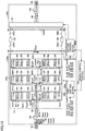
- FIGS. 1 and 2 are schematic configuration diagrams of a power conversion system according to Embodiment 1.
- the power conversion system is a BTB system in which a first power converter 1A and a second power converter 1B are directly connected, without a direct-current (DC) system and a DC transmission line in between.
- DC direct-current
- the power conversion system includes a power conversion device 150A, a power conversion device 150B, and a main control device 200.
- Power conversion device 150A includes a first power converter 1A which is a main circuit, a first control device 100A which controls first power converter 1A, an interconnection transformer 8A, and an alternating-current (AC) circuit breaker 13A.
- Power conversion device 150B includes: a second power converter 1B which is a main circuit; a second control device 100B which controls second power converter 1B; an interconnection transformer 8B; and an AC circuit breaker 13B.
- Main control device 200 is connected to first control device 100A and second control device 100B by communication lines, and controls first control device 100A and second control device 100B.
- First power converter 1A is connected to an AC system 9A.
- Second power converter 1B is connected to an AC system 9B.
- First positive DC terminal 2A and second positive DC terminal 2B are directly connected to each other by a line 50P which is a DC system, without a DC transmission line in between.
- a first negative DC terminal 3A and a second negative DC terminal 3B are directly connected to each other by a line 50N which is a DC system, without a DC transmission line in between.
- First power converter 1A and AC system 9A are interconnected, and second power converter 1B and AC system 9B are interconnected.
- first power converter 1A first power converter 1A
- second power converter 1B has the same configuration as first power converter 1A, and operates in the same manner.
- First power converter 1A converts power between a three-phase alternating current and a direct current.
- the AC side of first power converter 1A is connected to a three-phase AC system 9A, which is a three-phase AC circuit system, via interconnection transformer 8A and AC circuit breaker 13A.
- First power converter 1A is capable of converting an AC power from AC system 9A into a DC power, and supplying the DC power to the DC system, and converting a DC power from the DC system into an AC power and supplying the AC power to AC system 9A.
- Second power converter 1B converts power between a three-phase alternating current and a direct current.
- the AC side of second power converter 1B is connected to a three-phase AC system 9B, which is a three-phase AC circuit system, via interconnection transformer 8B.
- Second power converter 1B is capable of converting an AC power from AC system 9B into a DC power and supplying the DC power to the DC system, and converting a DC power from the DC system into an AC power and supplying the AC power to AC system 9B.
- First power converter 1A includes three phase arms 4UA, 4VA, 4WA.
- Three phase arms 4UA, 4VA, 4WA are connected in parallel between a positive DC bus PBL and a negative DC bus NBL.
- Positive DC bus PBL is connected to positive first DC terminal 2A
- negative DC bus NBL is connected to first negative DC terminal 3A.
- Arm 4UA includes a positive arm 5UA and a negative arm 6UA.
- Arm 4VA includes a positive arm 5VA and a negative arm 6VA.
- Arm 4WA includes a positive arm 5WA and a negative arm 6WA.
- Positive arm 5UA and negative arm 6UA are connected in series.
- An AC terminal 7UA which is a point of connection between positive arm 5UA and negative arm 6UA, is connected to a U-phase AC line UCA.
- Positive arm 5VA and negative arm 6VA are connected in series.
- An AC terminal 7VA which is a point of connection between positive arm 5VA and negative arm 6VA, is connected to a V-phase AC line VCA.
- Positive arm 5WA and negative arm 6WA are connected in series.
- An AC terminal 7WA which is a point of connection between positive arm 5WA and negative arm 6WA, is connected to a W-phase AC line WCA.
- Positive arms 5UA, 5VA, 5WA and negative arms 6UA, 6VA, 6WA each include one or more transducer cells 10A connected in series.
- Arm 4UA includes one or more transducer cells 10A connected in series and reactors 11UA, 12UA.
- Reactors 11UA, 12UA may be inserted anywhere within arm 4UA. As shown in FIG. 1 , one of reactors 11UA, 12UA may be inserted in positive arm 5UA and the other may be inserted in negative arm 6UA. Alternatively, both reactors 11UA, 12UA may be inserted in positive arm 5UA or in negative arm 6UA.
- Arm 4VA includes one or more transducer cells 10A connected in series and reactors 11VA, 12VA.
- Reactors 11VA, 12VA may be inserted anywhere within arm 4VA. As shown in FIG. 1 , one of reactors 11VA, 12VA may be inserted in positive arm 5VA, and the other may be inserted in negative arm 6VA. Alternatively, both reactors 11VA, 12VA may be inserted in positive arm 5VA or in negative arm 6VA.
- Arm 4WA includes one or more transducer cells 10A connected in series and reactors 11WA, 12WA.
- Reactors 11WA, 12WA may be inserted anywhere within arm 4WA. As shown in FIG. 1 , one of reactors 11WA, 12WA may be inserted in positive arm 5WA, and the other may be inserted in negative arm 6WA. Alternatively, both reactors 11WA, 12WA may be inserted in positive arm 5WA or in negative arm 6WA.
- First control device 100A includes a voltage command value generation unit 181 and a PWM (Pulse Width Modulation) circuitry 182.
- First control device 100A generates a gate signal, and controls transducer cells 10A included in positive arms 5UA, 5VA, 5WA and negative arms 6UA, 6VA, 6WA. A detailed configuration of first control device 100A will be described below.
- Positive arm currents ipuA, ipvA, ipwA flowing through positive arms 5UA, 5VA, 5WA are detected by current detectors 71pUA, 71pVA, 71pWA, respectively, and sent to control device 100.
- Negative arm currents inuA, invA, inwA flowing through negative arms 6UA, 6VA, 6WA are detected by current detectors 71nUA, 71nVA, 71nWA, respectively, and sent to first control device 100A.
- Three phase voltages VsuA, VsvA, VswA of AC system 9A are detected by voltage detectors 74UA, 74VA, 74WA and sent to first control device 100A.
- DC voltage VdcA between first positive DC terminal 2A and first negative DC terminal 3A is detected by a voltage detector 73A and sent to first control device 100A.
- DC voltage VdcB between second positive DC terminal 2B and second negative DC terminal 3B is detected by a voltage detector 73B and sent to main control device 200.
- the three phase AC currents of AC system 9A and DC currents may be detected by current detectors not shown, or determined by computing positive arm currents ipuA, ipvA, ipwA, and negative arm currents inuA, invA, inwA.
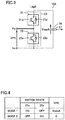
- FIG. 3 is a diagram representing a configuration example of transducer cell 10A according to Embodiment 1.
- a transducer cell 10B has the same configuration as transducer cell 10A.
- Transducer cell 10A has a half-bridge configuration.
- Transducer cell 10A includes a series body 23 and a DC capacitor 29 which are connected in parallel.
- series body 23 may be referred to as LegX.
- DC capacitor 29 smooths DC voltage.
- Series body 23 includes a switch 21 and a switch 22 which are connected in series.
- Switch 21 includes a semiconductor switching element 21s and a diode 21d connected in anti-parallel with semiconductor switching element 21s.
- Switch 22 includes a semiconductor switching element 22s and a diode 22d connected in anti-parallel with semiconductor switching element 22s.
- Self turn-off elements such as IGBT (Insulated Gate Bipolar Transistor) or GCT (Gate Commutated Turn-off Thyristor), are used as semiconductor switching elements 21s, 22s.
- semiconductor switching elements 21s, 22s switch on or off.
- transducer cell 10A In transducer cell 10A according to Embodiment 1, semiconductor switching elements 21s, 22s turn on or off, thereby causing the voltage across DC capacitor 29 or zero voltage to be output from terminals Po, No of semiconductor switching element 22s. While one transducer cell 10A and one transducer cell 10B have terminals Po, No in FIGS. 1 and 2 , the other transducer cells 10A and the other transducer cells 10B have terminals Po, No as well.
- Voltage VcapA across DC capacitor 29 included in transducer cell 10A is detected by a voltage detector 27 and sent to first control device 100A.
- FIG. 4 is a diagram representing a relationship between modes and operations of transducer cell 10A according to Embodiment 1.
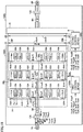
- FIG. 5 is a block diagram of a configuration example of first control device 100A.
- Second control device 100B has the same configuration as first control device 100A.
- First control device 100A includes a voltage command value generation unit 181 and a PWM circuitry 182.
- Voltage command value generation unit 181 includes a conversion unit 110, a DC control unit 120, an AC control unit 130, a positive arm command value computing unit 140, a negative arm command value computing unit 141, a positive cell individual control unit 155, and a negative cell individual control unit 156.
- PWM circuitry 182 includes a positive PWM circuit 160 and a negative PWM circuit 161.
- Conversion unit 110 converts detected current value and voltage value into signals for use in the control.
- Conversion unit 110 receives DC voltage VdcA between first positive DC terminal 2A and first negative DC terminal 3A, three phase voltages VsuA, VsvA, VswA of AC system 9A, positive arm currents ipuA, ipvA, ipwA, negative arm currents inuA, invA, inwA, and voltage VcapA across DC capacitor 29.
- Conversion unit 110 outputs, to DC control unit 120, DC voltage VdcA, and Idc flowing through line 50P between first positive DC terminal 2A and second positive DC terminal 2B.
- Conversion unit 110 outputs, to AC control unit 130, each phase AC current lac, each phase AC voltage Vs (VsuA, VsvA, VswA), and voltage average VcapA across DC capacitor 29.
- DC control unit 120 controls DC voltage and DC current.
- DC control unit 120 outputs a command value Kdc* to positive arm command value computing unit 140 and negative arm command value computing unit 141.
- AC control unit 130 controls AC voltage and AC current.
- AC control unit 130 outputs a command value Vac+* to positive arm command value computing unit 140, and outputs a command value Vac-* to negative arm command value computing unit 141.
- Positive arm command value computing unit 140 calculates a positive arm voltage command value V+*, based on command value Kdc* and command value Vac+*.
- Negative arm command value computing unit 141 calculates a negative arm voltage command value V-*, based on command value Kdc* and command value Vac-*.
- Positive cell individual control unit 155 calculates a voltage command value Vcell+* of each positive transducer cell 10A, based on positive arm voltage command value V+*.
- Negative cell individual control unit 156 calculates a voltage command value Vcell-* of each negative transducer cell 10A, based on negative arm voltage command value V-*.
- Positive PWM circuit 160 generates a gate signal for PWM control of each transducer cell 10A in positive arms 5UA, 5VA, 5WA, based on voltage command value Vcell+* of each positive transducer cell 10A.
- Negative PWM circuit 161 generates a gate signal for PWM control of each transducer cell 10A in negative arms 6UA, 6VA, 6WA, based on voltage command value Vcell-* of each negative transducer cell 10A.
- Semiconductor switching elements 21s, 22s in transducer cell 10A are control driven by the generated gate signal, thereby controlling the output voltage of first power converter 1A to a desired value.
- FIG. 6 is a flowchart representing a procedure for startup of the power conversion system according to Embodiment 1.
- FIG. 7 shows diagrams representing: AC voltages VsuA, VsvA, VswA in first power converter 1A versus time; DC voltage VdcA between first positive DC terminal 2A and first negative DC terminal 3A and its command value VdcA* versus time; an average of voltages of DC capacitors 29 included in first power converter 1A versus time; positive arm currents ipuA, ipvA, ipwA of first power converter 1A versus time; and negative arm currents inuA, invA, inwA of first power converter 1A versus time.
- FIG. 7 shows diagrams representing: AC voltages VsuA, VsvA, VswA in first power converter 1A versus time; DC voltage VdcA between first positive DC terminal 2A and first negative DC terminal 3A and its command value VdcA* versus time; an average of voltages of DC capacitors 29 included in first power converter 1A versus time; positive arm currents ipuA, ipvA, ip
- FIGS. 7 and 8 shows diagrams representing: AC voltages VsuB, VsvB, VswB in second power converter 1B versus time; DC voltage VdcB between second positive DC terminal 2B and second negative DC terminal 3B and its command value VdcB* versus time; an average of voltages of DC capacitors 29 included in second power converter 1B versus time; positive arm currents ipuB, ipvB, ipwB of second power converter 1B versus time; and negative arm currents inuB, invB, inwB of second power converter 1B versus time.
- pu represents a unit voltage or a unit current.
- DC voltage VdcA and DC voltage VdcB varies, depending on impedances between first positive DC terminal 2A and first negative DC terminal 3A and between second positive DC terminal 2B and second negative DC terminal 3B. If the impedances are close to zero, DC voltage VdcA and DC voltage VdcB are almost equal.
- first control device 100A and second control device 100B for first power converter 1A and second power converter 1B receive an AC circuit breaker turn-on command sent from main control device 200.
- first control device 100A and second control device 100B for first power converter 1A and second power converter 1B having received the AC circuit breaker turn-on command, turn on AC circuit breakers 13A, 13B.
- first power converter 1A and second power converter 1B are interconnected to AC systems 9A, 9B, charging of DC capacitors 29 of transducer cells 10A, 10B in first power converter 1A and second power converter 1B is started by a diode rectifier operation, and DC voltages VdcA, VdcB increase.
- the diode rectifier operation is an operation in which a current flows through only diodes 21d, 22d which are connected in anti-parallel with semiconductor switching elements 21s, 22s in first power converter 1A, second power converter 1B while semiconductor switching elements 21s, 22s in first power converter 1A, second power converter 1B are off.
- first control device 100A obtains voltages of DC capacitors 29 included in all the transducer cells 10A of first power converter 1A, and calculates an average (hereinafter, an average voltage VA) of the voltages.
- the average is used because the voltages of DC capacitors 29 included in all the transducer cells 10A are approximately the same value and a small amount of error is negligible.
- first control device 100A determines whether the initial charging of DC capacitors 29 included in first power converter 1A has completed, based on whether average voltage VA has reached an initial charging level VIF or whether an average voltage VA has been greater than or equal to initial charging level VIF for a few consecutive cycles.
- specifications [pu] of initial charging level VIF can be a value predetermined according to the following Equation (1), where V 1 [V] indicates a first power converter 1A side rated line AC voltage, Ncell indicates the number of transducer cells 10A per arm, and Vmx [V] indicates a rated capacitor voltage of transducer cell 10A.
- Equation (1) Equation (1), where V 1 [V] indicates a first power converter 1A side rated line AC voltage, Ncell indicates the number of transducer cells 10A per arm, and Vmx [V] indicates a rated capacitor voltage of transducer cell 10A.
- MATH 1 VIF 2 V l Ncell 1 Vmx
- the completion of the initial charging of DC capacitors 29 included in transducer cells 10A of first power converter 1A is determined because a drive device not shown in FIG. 3 uses the energy generated by the DC capacitors 29 included in transducer cells 10A to drive semiconductor switching elements 21s, 22s included in transducer cells 10A.
- Semiconductor switching elements 21s, 22s included in transducer cell 10A are not driven until the charging voltage of DC capacitors 29 has reached the initial charging voltage. In other words, semiconductor switching elements 21s, 22s can be driven once the completion of the initial charging is determined.
- the initial charging of DC capacitors 29 included in second power converter 1B may be completed or incomplete. Thus, the completion of the initial charging of DC capacitors 29 included in second power converter 1B is not determined.
- step S4 If the initial charging is determined to be incomplete at step S4 (S4: NO), the process returns to step S3, and first control device 100A repeats the process of determining the completion of the initial charging. If the initial charging of DC capacitors 29 is determined to be completed at step S4 (S4: YES), the process proceeds to step S5. As shown in the third row of FIG. 7 , S4 is determined as YES at time t1.
- step S5 first control device 100A notifies first control device 100A for first power converter 1A of an operation start command.
- first control device 100A for first power converter 1A having received the operation start command, generates voltage command values Vcell+*, Vcell-* for outputting an AC voltage to AC terminals 7UA, 7VA, 7WA and a first reference level to first DC terminals 2A, 3A.
- First control device 100A performs a PWM control on semiconductor switching elements 21s, 22s, based on voltage command values Vcell+*, Vcell-*.
- DC capacitors 29 are charged with power from AC system 9A simultaneously.
- the control command value for the average of the voltages of DC capacitors 29 versus time is configured as a ramp function RC having a constant rate of increase
- command value VdcA* for DC voltage VdcA between first positive DC terminal 2A and first negative DC terminal 3A is configured as a ramp function RD having a constant rate of increase, the ramp function RD being depending on ramp function RC.
- DC capacitors 29 of transducer cells 10B included in second power converter 1B are also charged with power from the DC system to constant levels with an increase of DC voltage VdcA.
- the average of the voltages of DC capacitors 29 and DC voltage VdcA are raised at a constant rate of increase because DC capacitor 29 rapidly receives energy from AC system 9A if they are raised rapidly, causing variations in voltage of AC system 9A.
- a value that does not cause variations in voltage of AC system 9A may be determined by a simulation or the like and set as the rate of increase.
- first control device 100A obtains the magnitude of DC voltage VdcA by measurement or computation.
- first control device 100A determines whether the raising of DC voltage VdcA to the first reference level has completed, based on the magnitude of DC voltage VdcA, specifically, based on whether DC voltage VdcA has reached the first reference level or whether DC voltage VdcA has been greater than or equal to the first reference level for a few consecutive cycles. If the raising of DC voltage VdcA to the first reference level is determined to be incomplete (S8: NO), the process returns to step S7, and first control device 100A repeats the process of determining whether the raising has completed. If the raising of DC voltage VdcA to the first reference level is determined to be completed (S8: YES), the process proceeds to step S9.
- DC voltage VdcA is raised to the first reference level at steps S7 and S8 in order to charge DC capacitors 29 included in second power converter 1B to a constant level. If the amount of charge in DC capacitors 29 included in second power converter 1B is low, an increased amount of voltage is reduced at the following step S9, which may cause first power converter 1A to overmodulate.
- the first reference level can be the rated voltage for first power converter 1A, or a voltage that is higher or smaller than the rated voltage by a few percentages.
- main control device 200 receives, from second control device 100B for second power converter 1B, a signal representing a level LB of the DC voltage that can be output from second power converter 1B, as information representing the status of second power converter 1B.
- first control device 100A for first power converter 1A receives level LB of the DC voltage from main control device 200.
- First control device 100A reduces DC voltage VdcA to LB at a constant rate of reduction.
- Command value VdcA* for DC voltage VdcA between first positive DC terminal 2A and first negative DC terminal 3A is configured as a ramp function having a constant rate of reduction, thereby causing DC voltage VdcA to fall at the constant rate of reduction (see times t3 to t4 in the second row of FIG. 7 and the second row of FIG. 8 ).
- first control device 100A obtains the magnitude of DC voltage VdcA by measurement or computation.
- first control device 100A determines whether the magnitude of VdcA has changed to level LB of the DC voltage that can be output from second power converter 1B obtained at step S9, based on whether the magnitude of DC voltage VdcA has reached level LB of the DC voltage or whether the magnitude of DC voltage VdcA has been at level LB of the DC voltage for a few consecutive cycles.
- step S12 If the magnitude of DC voltage VdcA is determined as not having changed to level LB of the DC voltage that can be output from second power converter 1B (S12: NO), the process returns to step S11, and first control device 100A repeats the process of determining the completion of the change. If the magnitude of DC voltage VdcA is determined as having changed to level LB of the DC voltage that can be output from second power converter 1B (S12: YES), the process proceeds to step S13. This can reduce the potential difference between DC voltage VdcA and DC voltage VdcB, thereby allowing for reduction of inrush current from first power converter 1A to second power converter 1B.
- second control device 100B for second power converter 1B receives an operation start command sent from main control device 200.
- Second control device 100B generates voltage command values Vcell+*, Vcell-* for outputting AC voltage to AC terminals 7UB, 7VB, 7WB and outputting, to second DC terminals 2B, 3B, level LB of the DC voltage that can be output from second power converter 1B and transmitted at step S9, and performs a PWM control of semiconductor switching elements 21s, 22s.
- DC capacitors 29 in second power converter 1B are simultaneously charged with power from AC system 9B.
- First control device 100A maintains the voltages of first DC terminals 2A, 3A at level LB of the DC voltage that can be output from second power converter 1B.
- DC voltage VdcB is raised to LB, not to the rating, for the sake of stable operation. If DC voltage VdcB is raised to the rating, a current flows through second power converter 1B due to the voltage difference between DC voltage VdcA and DC voltage VdcB, which needs to be prevented.
- second control device 100B obtains an average of voltages (hereinafter, average voltage VB) of DC capacitors 29 included in all the transducer cells 10B of second power converter 1B by measurement or computation.
- average voltage VB average voltage
- second control device 100B determines whether charging of DC capacitors 29 included in all the transducer cells 10B of second power converter 1B to a second reference level has completed, based on whether average voltage VB has reached the second reference level or whether average voltage VB has been at the second reference level for a few consecutive cycles. If charging of DC capacitors 29 to the second reference level is determined to be incomplete (S15: NO), the process returns to step S14, and second control device 100B repeats the operation of determining the completion of the charging. If charging of DC capacitors 29 to the second reference level is determined to be completed (S15: YES), the process proceeds to step S16.
- the second reference level can be the rated voltage for DC capacitors 29, or a voltage higher or smaller than the rated voltage by a few percentages.
- first control device 100A receives, from second control device 100B, information notifying that charging of DC capacitors 29 included in all the transducer cells 10B of second power converter 1B to the second reference level has completed, as information representing the status of second power converter 1B.
- First control device 100A raises command value VdcA* for DC voltage VdcA to a third reference level at a constant rate of change.
- Second control device 100B raises command value VdcB* for DC voltage VdcB to a fourth reference level at a constant rate of change.
- the third reference level can be the rated voltage for first power converter 1A, or a voltage higher or smaller than the rated voltage by a few percentages.
- the fourth reference level can be the rated voltage for second power converter 1B, or a voltage higher or smaller than the rated voltage by a few percentages. Note that, preferably, the third reference level and the fourth reference level are the same level for the prevention of inrush current caused by the potential difference between DC voltages VdcA and VdcB.
- first control device 100A obtains the magnitudes of DC voltages VdcA, VdcB by measurement or computation.
- first control device 100A and second control device 100B determine whether the raising of DC voltages VdcA, VdcB to the third reference level and the fourth reference level has completed, based on whether the magnitudes of DC voltages VdcA, VdcB have reached the third reference level and the fourth reference level or whether the magnitudes of DC voltages VdcA, VdcB have been at the third reference level and the fourth reference level for a few consecutive cycles.
- the process returns to step S17, and first control device 100A and second control device 100B repeat the processes of determining the completions of the raising. If the raising of DC voltages VdcA, VdcB to the third reference level and the fourth reference level is determined to be completed (S18: YES), the process proceeds to step S19.
- first power converter 1A converts an AC power into a DC power
- second power converter 1B converts a DC power into an AC power, thereby transmitting the power from AC system 9A to AC system 9B.
- FIG. 9 is a diagram representing a configuration of a transducer cell 10A according to Embodiment 2.
- a transducer cell 10B has the same configuration as transducer cell 10A.
- Transducer cell 10A includes a series body 35 and a series body 36, and a DC capacitor 39 which are connected in parallel.
- series body 35 may be referred to as LeX
- series body 36 may be referred to as LegY.
- DC capacitor 39 smooths DC voltage.
- Series body 35 includes a switch 31 and a switch 32 which are connected in series.
- Switch 31 includes a semiconductor switching element 31s and a diode 31d connected in anti-parallel with semiconductor switching element 31s.
- Switch 32 includes a semiconductor switching element 32s and a diode 32d connected in anti-parallel with semiconductor switching element 32s.
- Series body 36 includes a diode 33 and a switch 34 which are connected in series.
- Switch 34 includes a semiconductor switching element 34s and a diode 34d connected in anti-parallel with semiconductor switching element 34s.
- Self turn-off elements such as IGBT or GCT, are used as semiconductor switching elements 31s, 32s, 34s.
- semiconductor switching elements 31s, 32s, 34s turn on or off, thereby causing a positive voltage having the same polarity and substantially equal in magnitude to the voltage of DC capacitor 39 or zero voltage to be output from a terminal Po, which is a point of connection between semiconductor switching elements 31s, 32s, and terminal No, which is a point of connection between diode 33 and semiconductor switching element 34s.
- FIG. 10 is a diagram representing modes and operations of transducer cell 10A according to Embodiment 2.
- series body 36 includes a diode and a switch
- series body 35 may include a diode and a switch.
- FIG. 11 is a diagram representing a configuration example of a transducer cell 10A according to Embodiment 3.
- a transducer cell 10B has the same configuration as transducer cell 10A.
- Transducer cell 10A has a full-bridge configuration.
- Transducer cell 10A includes a series body 45, a series body 46, and a DC capacitor 49 which are connected in parallel.
- series body 45 may be referred to as LegX
- series body 46 may be referred to as LegZ.
- DC capacitor 49 smooths DC voltage.
- Series body 45 includes a switch 41 and a switch 42 which are connected in series.
- Switch 41 includes a semiconductor switching element 41s and a diode 41d connected in anti-parallel with semiconductor switching element 41s.
- Switch 42 includes a semiconductor switching element 42s and a diode 42d connected in anti-parallel with semiconductor switching element 42s.
- Series body 46 includes a switch 43 and a switch 44 which are connected in series.
- Switch 43 includes a semiconductor switching element 43s and a diode 43d connected in anti-parallel with semiconductor switching element 43s.
- Switch 44 includes a semiconductor switching element 44s and a diode 44d connected in anti-parallel with semiconductor switching element 44s.
- Self turn-off elements such as IGBT or GCT, are used as semiconductor switching elements 41s, 42s, 43s, 44s.
- semiconductor switching elements 41s, 42s, 43s, 44s turn on or off, thereby causing a positive voltage having the same polarity as the voltage across DC capacitor 49, a negative voltage having an opposite polarity to the voltage across DC capacitor 49, or zero voltage to be output from a terminal Po and a terminal No, the terminal Po being a point of connection between semiconductor switching elements 41s, 42s, the terminal No being a point of connection between semiconductor switching element 43s, 44s.
- FIG. 12 is a diagram representing modes and operations of transducer cell 10A according to Embodiment 3.
- a voltage between terminals Po, No is, generally, a voltage (-VcapA) across DC capacitor 49.
- semiconductor switching element 41s is off, semiconductor switching element 42s is on, semiconductor switching element 43s is off, and semiconductor switching element 44s is on.
- a voltage between terminals Po, No is generally zero voltage (0).
- FIG. 13 is a schematic configuration diagram of a power conversion system according to Embodiment 4.
- a first positive DC terminal 2A connected to a first power converter 1A, is connected to a DC transmission line 15P which is a DC system, via a DC circuit breaker 14PA.
- a first negative DC terminal 3A connected to first power converter 1A, is connected to a DC transmission line 15N which is a DC system, via a DC circuit breaker 14NA.
- FIG. 14 is a flowchart representing a procedure for startup of the power conversion system according to Embodiment 4.
- a first control device 100A and second control device 100B for first power converter 1A and second power converter 1B receive a DC circuit breaker turn-on command sent from a main control device 200.
- first control device 100A and second control device 100B for first power converter 1A and second power converter 1B having received the DC circuit breaker turn-on command, turn on DC circuit breakers 14PA, 14NA, 14PB, 14NB. This connects first power converter 1A and second power converter 1B through DC transmission lines 15P, 15N.
- first control device 100A and second control device 100B detect whether an answer back signal is sent, the answer back signal notifying that DC circuit breakers 14PA, 14NA, 14PB, 14N are turned on.
- step S24 based on the answer back signal, it is determined whether all the DC circuit breakers 14PA, 14NA, 14PB, 14NB are turned on. If the turning on of all the DC circuit breakers 14PA, 14NA, 14PB, 14NB is determined to be incomplete at step S23, the process returns to step S22, and first control device 100A and second control device 100B repeat, at regular intervals, the determination of the completion of turning on of DC circuit breakers 14PA, 14NA, 14PB, 14NB. At step S23, if the turning on of all the DC circuit breakers 14PA, 14NA, 14PB is determined to be completed, the process proceeds to steps S1 to S19 in FIG. 6 .
- inrush current that flows into the power converter upon startup can be reduced also in a power conversion system which includes a DC circuit breaker 14.
- FIG. 15 is a schematic configuration diagram of a power conversion system according to Embodiment 5.
- first control device 100A and second control device 100B directly communicate with each other, bypassing main control device 200.
- inrush current that flows into the power converter upon startup can be reduced, without requiring the precedence main control device 200.
- FIG. 16 is a schematic configuration diagram of a power conversion system according to Embodiment 6.
- the power conversion system is a three-terminal HVDC (High Voltage Direct Current) system. The same parts as those according to Embodiment 1 will not be described.
- a method for starting up the three-terminal HVDC system will be described from charging of capacitors with power from an AC system to a start of transmission of power.
- a first power converter 1A connects to an AC system 9A.
- First power converter 1A connected to first DC terminals 2A, 3A, is connected, via DC circuit breakers 14PA, 14NA, to DC transmission lines 15PA, 15NA which are DC systems.
- a second power converter 1B connects to an AC system 9B.
- Second power converter 1B connected to second DC terminals 2B, 3B, is connected, via DC circuit breakers 14PB, 14NB, to DC transmission lines 15PB, 15NB which are DC systems.
- a third power converter 1C connects to an AC system 9C.
- Third power converter 1C connected to third DC terminals 2C, 3C, is connected, via DC circuit breakers 14PC, 14NC, to DC transmission lines 15PC, 15NC which are DC systems.
- DC transmission line 15PA, DC transmission line 15PB, and DC transmission line 15PC are connected.
- DC transmission line 15NA, DC transmission line 15NB, and DC transmission line 15NC are connected.
- FIGS. 17 and 18 are flowcharts representing a procedure for startup of the power conversion system according to Embodiment 6.
- first power converter 1A, second power converter 1B, a first control device 100A for third power converter 1C, a second control device 100B, and third control device 100C receive a DC circuit breaker turn-on command sent from main control device 200.
- first control device 100A, second control device 100B, and third control device 100C for first power converter 1A, second power converter 1B, and third power converter 1C having received the DC circuit breaker turn-on command, turn on DC circuit breakers 14PA, 14NA, 14PB, 14NB, 14PC, 14NC.
- First power converter 1A and third power converter 1C are connected via DC transmission lines 15PA, 15PC, 15NA, 15NC.
- Second power converter 1B and third power converter 1C are connected via DC transmission lines 15PB, 15PC, 15NB, 15NC.
- first control device 100A, second control device 100B, and third control device 100C detect whether an answer back signal has been sent, the answer back signal notifying that DC circuit breakers 14PA, 14NA, 14PB, 14NB, 14PC, 14N are turned on.
- first control device 100A, second control device 100B, and third control device 100C determine whether all the DC circuit breakers 14PA, 14NA, 14PB, 14NB, 14PC, 14NC are turned on. It the turning on of all the DC circuit breakers 14PA, 14NA, 14PB, 14NB, 14PC, 14NC is determined to be incomplete at step S33, the process returns to step S32, and first control device 100A, second control device 100B, and third control device 100C repeat, at regular intervals, the process of determining of the completion of turning on of DC circuit breakers 14PA, 14NA, 14PB, 14NB, 14PC, 14NC.
- step S33 If the turning on of all the DC circuit breakers 14PA, 14NA, 14PB, 14NB, 14PC, 14NC is determined to be completed at step S33, the process proceeds to step S34.
- first control device 100A, second control device 100B, and third control device 100C for first power converter 1A, second power converter 1B, and third power converter 1C receive an AC circuit breaker turn-on command sent from main control device 200.
- first power converter 1A, second power converter 1B, and third power converter 1C are interconnected to AC systems 9A, 9B, 9C; DC voltages VdcA, VdcB, VdcC is increased by a diode rectifier operation; and charging of DC capacitors 29 included in transducer cells 10A, 10B, 10C of first power converter 1A, second power converter 1B, and third power converter 1C is started.
- first control device 100A obtains voltages of DC capacitors 29 included in all the transducer cells 10A of first power converter 1A, and calculates an average (hereinafter, average voltage VA) of the voltages.
- first control device 100A determines whether the initial charging of DC capacitors 29 included in first power converter 1A has been completed, based on whether average voltage VA has reached an initial charging level VIF or whether average voltage VA has been at initial charging level VIF for a few consecutive cycles.
- Initial charging level VIF can be determined in the same manner as Embodiment 1.
- step S37 If the initial charging is determined to be incomplete at step S37 (S37: NO), the process returns to step S36, and first control device 100A repeats the process of determining the completion of the initial charging. If the initial charging of DC capacitor 29 is determined to be completed at step S37 (S37: YES), the process proceeds to step S38.
- main control device 200 notifies first control device 100A for first power converter 1A of an operation start command.
- first control device 100A for first power converter 1A having received the operation start command, generates voltage command values Vcell+*, Vcell-* for outputting rated voltages to AC terminals 7UA, 7VA, 7WA and outputting a first reference level to first DC terminals 2A, 3A. Based on voltage command values Vcell+*, Vcell-*, first control device 100A performs a PWM control of semiconductor switching elements 21s, 22s. At this time, DC capacitor 29 is charged simultaneously.
- the control command value for the average of the voltages of DC capacitors 29 versus time is configured as a ramp function RC having a constant rate of increase
- command value VdcA* for DC voltage VdcA between first positive DC terminal 2A and first negative DC terminal 3A is configured as a ramp function RD having a constant rate of increase, the ramp function RD being depending on ramp function RC, thereby raising the average of voltages of DC capacitors 29 at the constant rate of increase and DC voltage VdcA at the constant rate of increase.
- first control device 100A obtains the magnitude of DC voltage VdcA by measurement or computation.
- first control device 100A determines whether the raising of DC voltage VdcA to the first reference level has completed, based on the magnitude of DC voltage VdcA, specifically, based on whether DC voltage VdcA has reached the first reference level or whether DC voltage VdcA has been at the first reference level for a few consecutive cycles. If the raising of DC voltage VdcA to the first reference level is determined to be incomplete (S41: NO), the process returns to step S40, and first control device 100A repeats the process of determining whether the raising has completed. If the raising of DC voltage VdcA to the first reference level is determined to be completed (S41: YES), and the process proceeds to step S42.
- the first reference level can be the rated voltage for first power converter 1A, or a voltage that is higher or smaller than the rated voltage by a few percentages.
- main control device 200 receives, from second control device 100B for second power converter 1B, a signal representing a level LB of the DC voltage that can be output from second power converter 1B, as information representing the status of second power converter 1B.
- Main control device 200 receives, from third control device 100C for third power converter 1C, a signal representing a level LC of the DC voltage that can be output from third power converter 1C, as information representing the status of third power converter 1C.
- the DC voltage levels LB and LC are compared, and a power converter corresponding to a greater DC voltage level is started up prior to the other.
- a description will be given, assuming that DC voltage level LB is greater than DC level LC.
- Level LB of the DC voltage can be determined in the same manner as Embodiment 1.
- first control device 100A for first power converter 1A reduces DC voltage VdcA at a constant rate of reduction.
- Command value VdcA* for DC voltage VdcA between first positive DC terminal 2A and first negative DC terminal 3A is configured as a ramp function having a constant rate of reduction, thereby causing DC voltage VdcA to fall at the constant rate of reduction.
- first control device 100A obtains the magnitude of DC voltage VdcA by measurement or computation.
- first control device 100A determines whether the magnitude of DC voltage VdcA has changed to level LB of the DC voltage that can be output from second power converter 1B obtained at step S42, based on whether the magnitude of DC voltage VdcA has reached level LB of the DC voltage or whether the magnitude of DC voltage VdcA has been at level LB of the DC voltage for a few consecutive cycles.
- step S45 If the magnitude of DC voltage VdcA is determined as not having changed to level LB of the DC voltage that can be output from second power converter 1B (S45: NO), the process returns to step S44, and first control device 100A repeats the process of determining the completion of the change. If the magnitude of DC voltage VdcA is determined as having changed to level LB of the DC voltage that can be output from second power converter 1B (S45: YES), the process proceeds to step S46.
- second control device 100B for second power converter 1B receives an operation start command sent from main control device 200.
- Second control device 100B generates voltage command values Vcell+*, Vcell-* for rated voltages to AC terminals 7UB, 7VB, 7WB and outputting, to second DC terminals 2B, 3B, level LB of the DC voltage that can be output from second power converter 1B and transmitted at step S42, and performs a PWM control of semiconductor switching elements 21s, 22s.
- DC capacitors 29 in second power converter 1B are charged simultaneously.
- First control device 100A maintains the voltages of first DC terminals 2A, 3A at level LB of the DC voltage that can be output from second power converter 1B. This increases the voltages of DC capacitors 29 in second power converter 1B at a constant rate of change.
- second control device 100B obtains an average of voltages (hereinafter, average voltage VB) of DC capacitors 29 included in all the transducer cells 10B of second power converter 1B by measurement or computation.
- average voltage VB average voltages
- second control device 100B determines whether charging of DC capacitors 29 included in all the transducer cells 10B of second power converter 1B to the second reference level has completed, based on whether average voltage VB has reached the second reference level or whether average voltage VB has been at the second reference level for a few consecutive cycles. If changing of DC capacitors 29 to the second reference level is determined to be incomplete (S48: NO), the process returns to step S47, and second control device 100B repeats the operation of determining the completion of the charging. If changing of DC capacitors 29 to the second reference level is determined to be completed (S48: YES), the process proceeds to step S49.
- the second reference level can be the rated voltage for DC capacitors 29, or a voltage higher or smaller than the rated voltage by a few percentages.
- first control device 100A receives, from second control device 100B, information notifying that charging of DC capacitors 29 included in all the transducer cells 10B of second power converter 1B to the second reference level has completed, as information representing the status of second power converter 1B.
- main control device 200 receives, from third control device 100C for third power converter 1C, a signal representing level LC of the DC voltage that can be output from third power converter 1C, as information representing the status of third power converter 1C.
- the information is sent to first control device 100A for first power converter 1A and second control device 100B for second power converter 1B.
- First control device 100A for first power converter 1A and second control device 100B for second power converter 1B reduce DC voltages VdcA, VdcB to level LC of the DC voltage at a constant rate of reduction.
- Command value VdcA* for DC voltage VdcA between first positive DC terminal 2A and first negative DC terminal 3A is configured as a ramp function having a constant rate of reduction, thereby causing DC voltage VdcA to fall at the constant rate of reduction.
- Command value VdcB* for DC voltage VdcB between second positive DC terminal 2B and first negative DC terminal 3B is configured as a ramp function having a constant rate of reduction, thereby causing DC voltage VdcB to fall at the constant rate of reduction.
- first control device 100A and second control device 100B obtain the magnitudes of DC voltages VdcA, VdcB by measurement or computation.
- first control device 100A and second control device 100B determine whether the magnitudes of DC voltages VdcA, VdcB have changed to level LC of the DC voltage that can be output from third power converter 1C obtained at step S42, based on whether the magnitudes of DC voltages VdcA, VdcB have reached level LC of the DC voltage or whether the magnitudes of DC voltages VdcA, VdcB have been at level LC of the DC voltage for a few consecutive cycles.
- step S51: NO If the magnitudes of DC voltages VdcA, VdcB are determined as not having changed to level LC of the DC voltage that can be output from third power converter 1C (S51: NO), the process returns to step S50, and first control device 100A and second control device 100B repeat the operation of determining the completion of the change. If the magnitudes of DC voltages VdcA, VdcB are determined as having changed to level LC of the DC voltage that can be output from third power converter 1C (S51: YES), the process proceeds to step S52.
- third control device 100C for third power converter 1C receives an operation start command sent from main control device 200.
- Third control device 100C generates voltage command values Vcell+*, Vcell-* for outputting rated voltages to AC terminals 7UB, 7VB, 7WB and outputting, to second DC terminals 2B, 3B, level LC of the DC voltage that can be output from third power converter 1C and transmitted at step S42, and performs a PWM control of semiconductor switching elements 21s, 22s.
- DC capacitors 29 in third power converter 1C are simultaneously charged.
- First control device 100A maintains the voltages of first DC terminals 2A, 3A at level LC of the DC voltage that can be output from third power converter 1C. This increases the voltages of DC capacitors 29 in third power converter 1C at a constant rate of change.
- third control device 100C obtains an average of voltages (hereinafter, average voltage VC) of DC capacitors 29 included in all the transducer cell 10C of third power converter 1C by measurement or computation.
- average voltage VC average voltage
- step S54 third control device 100C determines whether changing of DC capacitors 29 included in all the transducer cell 10C of third power converter 1C to the second reference level has completed, based on whether average voltage VC has reached the second reference level or whether average voltage VC have been at the second reference level for a few consecutive cycles. If charging of DC capacitors 29 to the second reference level is determined to be incomplete (S54: NO), the process returns to step S53, and third control device 100C repeats the operation of determining the completion of the charging. If changing of DC capacitors 29 to the second reference level is determined to be completed (S54: YES), the process proceeds to step S55.
- first control device 100A and second control device 100B receive, from third control device 100C, information notifying that charging of DC capacitors 29 included in all the transducer cells 10C of third power converter 1C to the second reference level has completed, as information representing the status of the second power converter 1C.
- First control device 100A raises command value VdcA* for DC voltage VdcA to a third reference level at a constant rate of change.
- Second control device 100B raises command value VdcB* for DC voltage VdcB to a fourth reference level at a constant rate of change.
- Third control device 100C raises command value VdcC* for the DC voltage VdcC to a fifth reference level at a constant rate of change.
- the third reference level can be the rated voltage for first power converter 1A, or a voltage higher or smaller than the rated voltage by a few percentages.
- the fourth reference level can be the rated voltage for second power converter 1B, or a voltage higher or smaller than the rated voltage by a few percentages.
- the fifth reference level can be the rated voltage for third power converter 1C, or a voltage higher or smaller than the rated voltage by a few percentages. Note that, preferably, the third reference level, the fourth reference level, and the fifth reference level are the same level for the prevention of inrush current caused by the potential differences between DC voltages VdcA, VdcB, VdcC.
- first control device 100A, second control device 100B, and third control device 100C obtain the magnitudes of DC voltages VdcA, VdcB, VdcC by measurement or computation.
- first control device 100A, second control device 100B, and third control device 100C determine whether the raising of DC voltages VdcA, VdcB, VdcC to the third reference level, the fourth reference level, and the fifth reference level has completed, based on whether the magnitudes DC voltages VdcA, VdcB, VdcC have reached the third reference level, the fourth reference level, and the fifth reference level or whether the magnitudes of DC voltages VdcA, VdcB, VdcC have been at the third reference level, the fourth reference level, and the fifth reference level for a few consecutive cycles.
- step S58 if the raising of DC voltages VdcA, VdcB, VdcC to the third reference level, the fourth reference level, and the fifth reference level is determined to be incomplete (S57: NO), the process returns to step S56, and first control device 100A, second control device 100B, and third control device 100C repeat the process of determining the completions of the raising. If the raising of the DC voltages VdcA, VdcB, VdcC to the third reference level, the fourth reference level, and the fifth reference level is determined to be completed (S57: YES), the process proceeds to step S58.
- step S58 the startup is completed and the process transitions to a DC power transmission initiation operation.
- first power converter 1A converts an AC power into a DC power
- second power converter 1B and third power converter 1C convert a DC power into an AC power, thereby transmitting the power from first power converter 1A to second power converter 1B and third power converter 1C.
- main control device 200 may select a power converter to be started up first, from among first power converter 1A, second power converter 1B, and third power converter 1C, based on the information on AC systems 9A, 9B, 9C. This allows the power conversion system to operate stably, and allows for reduction of the effects on the AC system, such as variations in voltage of the AC system when charging the capacitors.
- inrush current that flows into second power converters 1B, 1C can be reduced.
- first control device 100A, second control device 100B, and third control device 100C may directly communicate with each other, bypassing main control device 200.
Landscapes
- Engineering & Computer Science (AREA)
- Power Engineering (AREA)
- Inverter Devices (AREA)
- Rectifiers (AREA)
Applications Claiming Priority (1)
| Application Number | Priority Date | Filing Date | Title |
|---|---|---|---|
| PCT/JP2017/032686 WO2019049368A1 (ja) | 2017-09-11 | 2017-09-11 | 電力変換装置および電力変換システム |
Publications (3)
| Publication Number | Publication Date |
|---|---|
| EP3683948A1 true EP3683948A1 (de) | 2020-07-22 |
| EP3683948A4 EP3683948A4 (de) | 2020-10-21 |
| EP3683948B1 EP3683948B1 (de) | 2024-06-26 |
Family
ID=65634900
Family Applications (1)
| Application Number | Title | Priority Date | Filing Date |
|---|---|---|---|
| EP17924487.6A Active EP3683948B1 (de) | 2017-09-11 | 2017-09-11 | Stromumwandlungssystem |
Country Status (4)
| Country | Link |
|---|---|
| US (1) | US11121637B2 (de) |
| EP (1) | EP3683948B1 (de) |
| JP (1) | JP6873251B2 (de) |
| WO (1) | WO2019049368A1 (de) |
Families Citing this family (9)
| Publication number | Priority date | Publication date | Assignee | Title |
|---|---|---|---|---|
| WO2019161907A1 (en) * | 2018-02-23 | 2019-08-29 | Abb Schweiz Ag | Energization of a converter including a mix of half-bridge and full-bridge submodules |
| US12322969B2 (en) | 2020-08-21 | 2025-06-03 | Mitsubishi Electric Corporation | Power conversion system |
| CN115989625A (zh) * | 2020-08-28 | 2023-04-18 | 日立能源瑞士股份公司 | 用于操作转换器的方法、转换器以及计算机程序产品 |
| US11424692B2 (en) * | 2020-12-23 | 2022-08-23 | Hamilton Sundstrand Corporation | Multi-level single-phase AC-to-DC converter |
| JP2022134479A (ja) * | 2021-03-03 | 2022-09-15 | 株式会社東芝 | 多端子直流送電システム |
| JP7497315B2 (ja) * | 2021-03-03 | 2024-06-10 | 株式会社東芝 | 多端子直流送電システム |
| CN118054668A (zh) | 2022-11-09 | 2024-05-17 | 台达电子企业管理(上海)有限公司 | 多电平转换电路及其飞跨电容电压的控制方法 |
| CN118017828A (zh) | 2022-11-09 | 2024-05-10 | 台达电子企业管理(上海)有限公司 | 多电平转换电路及其飞跨电容电压的控制方法 |
| CN118017851A (zh) * | 2022-11-09 | 2024-05-10 | 台达电子企业管理(上海)有限公司 | 多电平交流或直流/直流转换电路及其控制方法 |
Family Cites Families (20)
| Publication number | Priority date | Publication date | Assignee | Title |
|---|---|---|---|---|
| JPH0775341A (ja) * | 1993-09-06 | 1995-03-17 | Hitachi Ltd | 自励式送電システムの運転方法および運転制御装置 |
| JP4287031B2 (ja) * | 2000-07-14 | 2009-07-01 | 株式会社日立製作所 | 自励式直流送電システムの制御方法及び装置 |
| US8018748B2 (en) * | 2007-11-14 | 2011-09-13 | General Electric Company | Method and system to convert direct current (DC) to alternating current (AC) using a photovoltaic inverter |
| CN102377324B (zh) * | 2011-10-18 | 2013-09-04 | 吕遥 | 适合于高压应用的变流桥臂及其应用系统 |
| US9219426B2 (en) * | 2012-02-09 | 2015-12-22 | Hitachi, Ltd. | Switching element, power converter, direct current transmission system, current control device, method of controlling power converter, and method of controlling current in voltage source converter |
| JP5766356B2 (ja) * | 2012-08-08 | 2015-08-19 | 三菱電機株式会社 | 電力変換装置 |
| JP5993675B2 (ja) * | 2012-09-14 | 2016-09-14 | 株式会社日立製作所 | 電力変換装置,電力変換システム及び電力変換装置の制御方法 |
| DK2887526T3 (da) * | 2013-12-19 | 2019-06-24 | Abb Schweiz Ag | Fremgangsmåde og strømretter til at bestemme forringelse af en cellekondensator i en omformercelle |
| WO2016012060A1 (en) * | 2014-07-22 | 2016-01-28 | Abb Technology Ltd | A multilevel converter with reduced ac fault handling rating |
| WO2016056072A1 (ja) * | 2014-10-08 | 2016-04-14 | 三菱電機株式会社 | 電力変換装置 |
| EP3026803A1 (de) * | 2014-11-25 | 2016-06-01 | Alstom Technology Ltd | Anfahren von HVDC-Wandlern |
| EP3070799B1 (de) * | 2015-03-16 | 2018-11-21 | General Electric Technology GmbH | Inbetriebsetzung von hvdc-netzwerken |
| EP3070827B1 (de) * | 2015-03-16 | 2022-09-07 | General Electric Technology GmbH | Inbetriebsetzung von hvdc-netzwerken |
| JP6411925B2 (ja) | 2015-03-18 | 2018-10-24 | 株式会社日立製作所 | 電力変換装置 |
| WO2016191187A1 (en) * | 2015-05-27 | 2016-12-01 | University Of Pittsburgh-Of The Commonwealth System Of Higher Education | Communication-less fault section identification for hybrid hvdc transmission systems |
| CN106787875B (zh) * | 2015-11-20 | 2019-12-17 | 台达电子企业管理(上海)有限公司 | 脉冲驱动系统及脉冲驱动方法 |
| KR101629397B1 (ko) * | 2015-12-03 | 2016-06-13 | 연세대학교 산학협력단 | 비대칭 모듈러 멀티레벨 컨버터 제어 장치 및 방법 |
| CN107276378B (zh) * | 2016-04-08 | 2019-03-15 | 台达电子企业管理(上海)有限公司 | 预先充电控制方法 |
| US10936036B2 (en) * | 2016-09-26 | 2021-03-02 | Embedderment Ab | Soft-start switch circuits using separated power supply paths and related methods and systems |
| US10361624B2 (en) * | 2016-12-06 | 2019-07-23 | Infineon Technologies Austria Ag | Multi-cell power converter with improved start-up routine |
-
2017
- 2017-09-11 JP JP2019540285A patent/JP6873251B2/ja active Active
- 2017-09-11 WO PCT/JP2017/032686 patent/WO2019049368A1/ja not_active Ceased
- 2017-09-11 EP EP17924487.6A patent/EP3683948B1/de active Active
- 2017-09-11 US US16/631,196 patent/US11121637B2/en active Active
Also Published As
| Publication number | Publication date |
|---|---|
| WO2019049368A1 (ja) | 2019-03-14 |
| JP6873251B2 (ja) | 2021-05-19 |
| EP3683948B1 (de) | 2024-06-26 |
| JPWO2019049368A1 (ja) | 2020-08-06 |
| EP3683948A4 (de) | 2020-10-21 |
| US11121637B2 (en) | 2021-09-14 |
| US20200220471A1 (en) | 2020-07-09 |
Similar Documents
| Publication | Publication Date | Title |
|---|---|---|
| EP3683948B1 (de) | Stromumwandlungssystem | |
| US8228699B2 (en) | Power converting apparatus including half-bridge inverters connected between positive and negative terminals of a DC power supply | |
| EP2795780B1 (de) | Schwarzstart eines modularen multilevelumrichters mit spannungszwischenkreisen | |
| EP3836377B1 (de) | Stromumwandlungsvorrichtung | |
| TW504891B (en) | PWM pulse control method | |
| US11601064B2 (en) | Power conversion device having a frequency of a first control signal higher than a frequency of a second control signal | |
| EP3641123B1 (de) | Stromwandlungsvorrichtung | |
| EP4030612B1 (de) | Stromumwandlungsvorrichtung | |
| EP3633841A1 (de) | Stromwandlungsvorrichtung | |
| US9130481B2 (en) | Power converting appartatus | |
| CN103546055B (zh) | 多级电力变换电路的控制方法 | |
| EP0152595A1 (de) | Regelgerät für ein Gleichstrom-Energieübertragungssystem | |
| EP3890134B1 (de) | Leistungssteuerungssystem | |
| EP3637573B1 (de) | Leistungssteuerungssystem und steuerungsvorrichtung | |
| JP6779424B1 (ja) | 電力変換装置 | |
| EP3745582A1 (de) | Stromumwandlungsvorrichtung | |
| EP2677654A1 (de) | Inverterschaltung | |
| EP1643626A2 (de) | Gleichstromversorgungsgerät und Regelungsverfahren für dasselbe, und ein Kompressorantriebsgerät | |
| EP3661043A1 (de) | Modularer mehrpunktumrichter mit parallelen umrichterarmen in den einzelnen phasen und inter-arm kreisströmen | |
| US12381397B2 (en) | Power conversion system and control device for same | |
| JP2000287453A (ja) | 多重電力変換装置 | |
| CN105391308A (zh) | 矩阵变换器、矩阵变换器的控制装置及矩阵变换器的控制方法 | |
| EP4475373A1 (de) | Leistungssteuerungssystem | |
| JP2000308361A (ja) | 中性点クランプ型電力変換装置 | |
| JP7266373B2 (ja) | 電力変換装置 |
Legal Events
| Date | Code | Title | Description |
|---|---|---|---|
| STAA | Information on the status of an ep patent application or granted ep patent |
Free format text: STATUS: THE INTERNATIONAL PUBLICATION HAS BEEN MADE |
|
| PUAI | Public reference made under article 153(3) epc to a published international application that has entered the european phase |
Free format text: ORIGINAL CODE: 0009012 |
|
| STAA | Information on the status of an ep patent application or granted ep patent |
Free format text: STATUS: REQUEST FOR EXAMINATION WAS MADE |
|
| 17P | Request for examination filed |
Effective date: 20200217 |
|
| AK | Designated contracting states |
Kind code of ref document: A1 Designated state(s): AL AT BE BG CH CY CZ DE DK EE ES FI FR GB GR HR HU IE IS IT LI LT LU LV MC MK MT NL NO PL PT RO RS SE SI SK SM TR |
|
| AX | Request for extension of the european patent |
Extension state: BA ME |
|
| A4 | Supplementary search report drawn up and despatched |
Effective date: 20200917 |
|
| RIC1 | Information provided on ipc code assigned before grant |
Ipc: H02M 7/12 20060101AFI20200911BHEP Ipc: H02M 1/36 20070101ALI20200911BHEP Ipc: H02M 7/48 20070101ALI20200911BHEP Ipc: H02M 5/458 20060101ALI20200911BHEP Ipc: H02M 7/217 20060101ALI20200911BHEP Ipc: H02M 7/483 20070101ALI20200911BHEP |
|
| DAV | Request for validation of the european patent (deleted) | ||
| DAX | Request for extension of the european patent (deleted) | ||
| GRAP | Despatch of communication of intention to grant a patent |
Free format text: ORIGINAL CODE: EPIDOSNIGR1 |
|
| STAA | Information on the status of an ep patent application or granted ep patent |
Free format text: STATUS: GRANT OF PATENT IS INTENDED |
|
| INTG | Intention to grant announced |
Effective date: 20230913 |
|
| GRAJ | Information related to disapproval of communication of intention to grant by the applicant or resumption of examination proceedings by the epo deleted |
Free format text: ORIGINAL CODE: EPIDOSDIGR1 |
|
| STAA | Information on the status of an ep patent application or granted ep patent |
Free format text: STATUS: REQUEST FOR EXAMINATION WAS MADE |
|
| GRAP | Despatch of communication of intention to grant a patent |
Free format text: ORIGINAL CODE: EPIDOSNIGR1 |
|
| STAA | Information on the status of an ep patent application or granted ep patent |
Free format text: STATUS: GRANT OF PATENT IS INTENDED |
|
| INTC | Intention to grant announced (deleted) | ||
| INTG | Intention to grant announced |
Effective date: 20240205 |
|
| GRAS | Grant fee paid |
Free format text: ORIGINAL CODE: EPIDOSNIGR3 |
|
| GRAA | (expected) grant |
Free format text: ORIGINAL CODE: 0009210 |
|
| STAA | Information on the status of an ep patent application or granted ep patent |
Free format text: STATUS: THE PATENT HAS BEEN GRANTED |
|
| AK | Designated contracting states |
Kind code of ref document: B1 Designated state(s): AL AT BE BG CH CY CZ DE DK EE ES FI FR GB GR HR HU IE IS IT LI LT LU LV MC MK MT NL NO PL PT RO RS SE SI SK SM TR |
|
| REG | Reference to a national code |
Ref country code: GB Ref legal event code: FG4D |
|
| REG | Reference to a national code |
Ref country code: CH Ref legal event code: EP |
|
| REG | Reference to a national code |
Ref country code: DE Ref legal event code: R096 Ref document number: 602017082907 Country of ref document: DE |
|
| REG | Reference to a national code |
Ref country code: SE Ref legal event code: TRGR |
|
| PG25 | Lapsed in a contracting state [announced via postgrant information from national office to epo] |
Ref country code: BG Free format text: LAPSE BECAUSE OF FAILURE TO SUBMIT A TRANSLATION OF THE DESCRIPTION OR TO PAY THE FEE WITHIN THE PRESCRIBED TIME-LIMIT Effective date: 20240626 |
|
| PG25 | Lapsed in a contracting state [announced via postgrant information from national office to epo] |
Ref country code: HR Free format text: LAPSE BECAUSE OF FAILURE TO SUBMIT A TRANSLATION OF THE DESCRIPTION OR TO PAY THE FEE WITHIN THE PRESCRIBED TIME-LIMIT Effective date: 20240626 Ref country code: FI Free format text: LAPSE BECAUSE OF FAILURE TO SUBMIT A TRANSLATION OF THE DESCRIPTION OR TO PAY THE FEE WITHIN THE PRESCRIBED TIME-LIMIT Effective date: 20240626 |
|
| REG | Reference to a national code |
Ref country code: LT Ref legal event code: MG9D |
|
| PG25 | Lapsed in a contracting state [announced via postgrant information from national office to epo] |
Ref country code: GR Free format text: LAPSE BECAUSE OF FAILURE TO SUBMIT A TRANSLATION OF THE DESCRIPTION OR TO PAY THE FEE WITHIN THE PRESCRIBED TIME-LIMIT Effective date: 20240927 |
|
| PG25 | Lapsed in a contracting state [announced via postgrant information from national office to epo] |
Ref country code: LV Free format text: LAPSE BECAUSE OF FAILURE TO SUBMIT A TRANSLATION OF THE DESCRIPTION OR TO PAY THE FEE WITHIN THE PRESCRIBED TIME-LIMIT Effective date: 20240626 |
|
| REG | Reference to a national code |
Ref country code: NL Ref legal event code: MP Effective date: 20240626 |
|
| PG25 | Lapsed in a contracting state [announced via postgrant information from national office to epo] |
Ref country code: NO Free format text: LAPSE BECAUSE OF FAILURE TO SUBMIT A TRANSLATION OF THE DESCRIPTION OR TO PAY THE FEE WITHIN THE PRESCRIBED TIME-LIMIT Effective date: 20240926 Ref country code: LV Free format text: LAPSE BECAUSE OF FAILURE TO SUBMIT A TRANSLATION OF THE DESCRIPTION OR TO PAY THE FEE WITHIN THE PRESCRIBED TIME-LIMIT Effective date: 20240626 Ref country code: HR Free format text: LAPSE BECAUSE OF FAILURE TO SUBMIT A TRANSLATION OF THE DESCRIPTION OR TO PAY THE FEE WITHIN THE PRESCRIBED TIME-LIMIT Effective date: 20240626 Ref country code: GR Free format text: LAPSE BECAUSE OF FAILURE TO SUBMIT A TRANSLATION OF THE DESCRIPTION OR TO PAY THE FEE WITHIN THE PRESCRIBED TIME-LIMIT Effective date: 20240927 Ref country code: FI Free format text: LAPSE BECAUSE OF FAILURE TO SUBMIT A TRANSLATION OF THE DESCRIPTION OR TO PAY THE FEE WITHIN THE PRESCRIBED TIME-LIMIT Effective date: 20240626 Ref country code: BG Free format text: LAPSE BECAUSE OF FAILURE TO SUBMIT A TRANSLATION OF THE DESCRIPTION OR TO PAY THE FEE WITHIN THE PRESCRIBED TIME-LIMIT Effective date: 20240626 Ref country code: RS Free format text: LAPSE BECAUSE OF FAILURE TO SUBMIT A TRANSLATION OF THE DESCRIPTION OR TO PAY THE FEE WITHIN THE PRESCRIBED TIME-LIMIT Effective date: 20240926 |
|
| PG25 | Lapsed in a contracting state [announced via postgrant information from national office to epo] |
Ref country code: NL Free format text: LAPSE BECAUSE OF FAILURE TO SUBMIT A TRANSLATION OF THE DESCRIPTION OR TO PAY THE FEE WITHIN THE PRESCRIBED TIME-LIMIT Effective date: 20240626 |
|
| REG | Reference to a national code |
Ref country code: AT Ref legal event code: MK05 Ref document number: 1698531 Country of ref document: AT Kind code of ref document: T Effective date: 20240626 |
|
| PG25 | Lapsed in a contracting state [announced via postgrant information from national office to epo] |
Ref country code: NL Free format text: LAPSE BECAUSE OF FAILURE TO SUBMIT A TRANSLATION OF THE DESCRIPTION OR TO PAY THE FEE WITHIN THE PRESCRIBED TIME-LIMIT Effective date: 20240626 |
|
| PG25 | Lapsed in a contracting state [announced via postgrant information from national office to epo] |
Ref country code: PT Free format text: LAPSE BECAUSE OF FAILURE TO SUBMIT A TRANSLATION OF THE DESCRIPTION OR TO PAY THE FEE WITHIN THE PRESCRIBED TIME-LIMIT Effective date: 20241028 |
|
| PG25 | Lapsed in a contracting state [announced via postgrant information from national office to epo] |
Ref country code: PT Free format text: LAPSE BECAUSE OF FAILURE TO SUBMIT A TRANSLATION OF THE DESCRIPTION OR TO PAY THE FEE WITHIN THE PRESCRIBED TIME-LIMIT Effective date: 20241028 |
|
| PG25 | Lapsed in a contracting state [announced via postgrant information from national office to epo] |
Ref country code: PL Free format text: LAPSE BECAUSE OF FAILURE TO SUBMIT A TRANSLATION OF THE DESCRIPTION OR TO PAY THE FEE WITHIN THE PRESCRIBED TIME-LIMIT Effective date: 20240626 |
|
| PG25 | Lapsed in a contracting state [announced via postgrant information from national office to epo] |
Ref country code: EE Free format text: LAPSE BECAUSE OF FAILURE TO SUBMIT A TRANSLATION OF THE DESCRIPTION OR TO PAY THE FEE WITHIN THE PRESCRIBED TIME-LIMIT Effective date: 20240626 |
|
| PG25 | Lapsed in a contracting state [announced via postgrant information from national office to epo] |
Ref country code: AT Free format text: LAPSE BECAUSE OF FAILURE TO SUBMIT A TRANSLATION OF THE DESCRIPTION OR TO PAY THE FEE WITHIN THE PRESCRIBED TIME-LIMIT Effective date: 20240626 Ref country code: IS Free format text: LAPSE BECAUSE OF FAILURE TO SUBMIT A TRANSLATION OF THE DESCRIPTION OR TO PAY THE FEE WITHIN THE PRESCRIBED TIME-LIMIT Effective date: 20241026 |
|
| PG25 | Lapsed in a contracting state [announced via postgrant information from national office to epo] |
Ref country code: CZ Free format text: LAPSE BECAUSE OF FAILURE TO SUBMIT A TRANSLATION OF THE DESCRIPTION OR TO PAY THE FEE WITHIN THE PRESCRIBED TIME-LIMIT Effective date: 20240626 |
|
| PG25 | Lapsed in a contracting state [announced via postgrant information from national office to epo] |
Ref country code: RO Free format text: LAPSE BECAUSE OF FAILURE TO SUBMIT A TRANSLATION OF THE DESCRIPTION OR TO PAY THE FEE WITHIN THE PRESCRIBED TIME-LIMIT Effective date: 20240626 Ref country code: SK Free format text: LAPSE BECAUSE OF FAILURE TO SUBMIT A TRANSLATION OF THE DESCRIPTION OR TO PAY THE FEE WITHIN THE PRESCRIBED TIME-LIMIT Effective date: 20240626 |
|
| PG25 | Lapsed in a contracting state [announced via postgrant information from national office to epo] |
Ref country code: SM Free format text: LAPSE BECAUSE OF FAILURE TO SUBMIT A TRANSLATION OF THE DESCRIPTION OR TO PAY THE FEE WITHIN THE PRESCRIBED TIME-LIMIT Effective date: 20240626 Ref country code: ES Free format text: LAPSE BECAUSE OF FAILURE TO SUBMIT A TRANSLATION OF THE DESCRIPTION OR TO PAY THE FEE WITHIN THE PRESCRIBED TIME-LIMIT Effective date: 20240626 |
|
| PG25 | Lapsed in a contracting state [announced via postgrant information from national office to epo] |
Ref country code: SM Free format text: LAPSE BECAUSE OF FAILURE TO SUBMIT A TRANSLATION OF THE DESCRIPTION OR TO PAY THE FEE WITHIN THE PRESCRIBED TIME-LIMIT Effective date: 20240626 Ref country code: SK Free format text: LAPSE BECAUSE OF FAILURE TO SUBMIT A TRANSLATION OF THE DESCRIPTION OR TO PAY THE FEE WITHIN THE PRESCRIBED TIME-LIMIT Effective date: 20240626 Ref country code: RO Free format text: LAPSE BECAUSE OF FAILURE TO SUBMIT A TRANSLATION OF THE DESCRIPTION OR TO PAY THE FEE WITHIN THE PRESCRIBED TIME-LIMIT Effective date: 20240626 Ref country code: PL Free format text: LAPSE BECAUSE OF FAILURE TO SUBMIT A TRANSLATION OF THE DESCRIPTION OR TO PAY THE FEE WITHIN THE PRESCRIBED TIME-LIMIT Effective date: 20240626 Ref country code: IS Free format text: LAPSE BECAUSE OF FAILURE TO SUBMIT A TRANSLATION OF THE DESCRIPTION OR TO PAY THE FEE WITHIN THE PRESCRIBED TIME-LIMIT Effective date: 20241026 Ref country code: ES Free format text: LAPSE BECAUSE OF FAILURE TO SUBMIT A TRANSLATION OF THE DESCRIPTION OR TO PAY THE FEE WITHIN THE PRESCRIBED TIME-LIMIT Effective date: 20240626 Ref country code: EE Free format text: LAPSE BECAUSE OF FAILURE TO SUBMIT A TRANSLATION OF THE DESCRIPTION OR TO PAY THE FEE WITHIN THE PRESCRIBED TIME-LIMIT Effective date: 20240626 Ref country code: CZ Free format text: LAPSE BECAUSE OF FAILURE TO SUBMIT A TRANSLATION OF THE DESCRIPTION OR TO PAY THE FEE WITHIN THE PRESCRIBED TIME-LIMIT Effective date: 20240626 Ref country code: AT Free format text: LAPSE BECAUSE OF FAILURE TO SUBMIT A TRANSLATION OF THE DESCRIPTION OR TO PAY THE FEE WITHIN THE PRESCRIBED TIME-LIMIT Effective date: 20240626 |
|
| PG25 | Lapsed in a contracting state [announced via postgrant information from national office to epo] |
Ref country code: IT Free format text: LAPSE BECAUSE OF FAILURE TO SUBMIT A TRANSLATION OF THE DESCRIPTION OR TO PAY THE FEE WITHIN THE PRESCRIBED TIME-LIMIT Effective date: 20240626 |
|
| REG | Reference to a national code |
Ref country code: DE Ref legal event code: R097 Ref document number: 602017082907 Country of ref document: DE |
|
| PG25 | Lapsed in a contracting state [announced via postgrant information from national office to epo] |
Ref country code: DK Free format text: LAPSE BECAUSE OF FAILURE TO SUBMIT A TRANSLATION OF THE DESCRIPTION OR TO PAY THE FEE WITHIN THE PRESCRIBED TIME-LIMIT Effective date: 20240626 |
|
| PG25 | Lapsed in a contracting state [announced via postgrant information from national office to epo] |
Ref country code: MC Free format text: LAPSE BECAUSE OF FAILURE TO SUBMIT A TRANSLATION OF THE DESCRIPTION OR TO PAY THE FEE WITHIN THE PRESCRIBED TIME-LIMIT Effective date: 20240626 |
|
| REG | Reference to a national code |
Ref country code: CH Ref legal event code: PL |
|
| PLBE | No opposition filed within time limit |
Free format text: ORIGINAL CODE: 0009261 |
|
| STAA | Information on the status of an ep patent application or granted ep patent |
Free format text: STATUS: NO OPPOSITION FILED WITHIN TIME LIMIT |
|
| PG25 | Lapsed in a contracting state [announced via postgrant information from national office to epo] |
Ref country code: LU Free format text: LAPSE BECAUSE OF NON-PAYMENT OF DUE FEES Effective date: 20240911 |
|
| 26N | No opposition filed |
Effective date: 20250327 |
|
| REG | Reference to a national code |
Ref country code: BE Ref legal event code: MM Effective date: 20240930 |
|
| PG25 | Lapsed in a contracting state [announced via postgrant information from national office to epo] |
Ref country code: BE Free format text: LAPSE BECAUSE OF NON-PAYMENT OF DUE FEES Effective date: 20240930 |
|
| PG25 | Lapsed in a contracting state [announced via postgrant information from national office to epo] |
Ref country code: CH Free format text: LAPSE BECAUSE OF NON-PAYMENT OF DUE FEES Effective date: 20240930 |
|
| PG25 | Lapsed in a contracting state [announced via postgrant information from national office to epo] |
Ref country code: IE Free format text: LAPSE BECAUSE OF NON-PAYMENT OF DUE FEES Effective date: 20240911 |
|
| P01 | Opt-out of the competence of the unified patent court (upc) registered |
Free format text: CASE NUMBER: UPC_APP_4903_3683948/2025 Effective date: 20250827 |
|
| PGFP | Annual fee paid to national office [announced via postgrant information from national office to epo] |
Ref country code: DE Payment date: 20250730 Year of fee payment: 9 |
|
| PGFP | Annual fee paid to national office [announced via postgrant information from national office to epo] |
Ref country code: GB Payment date: 20250731 Year of fee payment: 9 |
|
| PGFP | Annual fee paid to national office [announced via postgrant information from national office to epo] |
Ref country code: FR Payment date: 20250808 Year of fee payment: 9 |
|
| PGFP | Annual fee paid to national office [announced via postgrant information from national office to epo] |
Ref country code: SE Payment date: 20250728 Year of fee payment: 9 |
|
| PG25 | Lapsed in a contracting state [announced via postgrant information from national office to epo] |
Ref country code: CY Free format text: LAPSE BECAUSE OF FAILURE TO SUBMIT A TRANSLATION OF THE DESCRIPTION OR TO PAY THE FEE WITHIN THE PRESCRIBED TIME-LIMIT; INVALID AB INITIO Effective date: 20170911 |
|
| PG25 | Lapsed in a contracting state [announced via postgrant information from national office to epo] |
Ref country code: HU Free format text: LAPSE BECAUSE OF FAILURE TO SUBMIT A TRANSLATION OF THE DESCRIPTION OR TO PAY THE FEE WITHIN THE PRESCRIBED TIME-LIMIT; INVALID AB INITIO Effective date: 20170911 |