EP3686323A1 - Substrat monocristallin de nitrure du groupe iii - Google Patents
Substrat monocristallin de nitrure du groupe iii Download PDFInfo
- Publication number
- EP3686323A1 EP3686323A1 EP18857897.5A EP18857897A EP3686323A1 EP 3686323 A1 EP3686323 A1 EP 3686323A1 EP 18857897 A EP18857897 A EP 18857897A EP 3686323 A1 EP3686323 A1 EP 3686323A1
- Authority
- EP
- European Patent Office
- Prior art keywords
- group iii
- single crystal
- substrate
- iii nitride
- nitride single
- Prior art date
- Legal status (The legal status is an assumption and is not a legal conclusion. Google has not performed a legal analysis and makes no representation as to the accuracy of the status listed.)
- Granted
Links
Images


Classifications
-
- C—CHEMISTRY; METALLURGY
- C30—CRYSTAL GROWTH
- C30B—SINGLE-CRYSTAL GROWTH; UNIDIRECTIONAL SOLIDIFICATION OF EUTECTIC MATERIAL OR UNIDIRECTIONAL DEMIXING OF EUTECTOID MATERIAL; REFINING BY ZONE-MELTING OF MATERIAL; PRODUCTION OF A HOMOGENEOUS POLYCRYSTALLINE MATERIAL WITH DEFINED STRUCTURE; SINGLE CRYSTALS OR HOMOGENEOUS POLYCRYSTALLINE MATERIAL WITH DEFINED STRUCTURE; AFTER-TREATMENT OF SINGLE CRYSTALS OR A HOMOGENEOUS POLYCRYSTALLINE MATERIAL WITH DEFINED STRUCTURE; APPARATUS THEREFOR
- C30B25/00—Single-crystal growth by chemical reaction of reactive gases, e.g. chemical vapour-deposition growth
- C30B25/02—Epitaxial-layer growth
- C30B25/18—Epitaxial-layer growth characterised by the substrate
- C30B25/186—Epitaxial-layer growth characterised by the substrate being specially pre-treated by, e.g. chemical or physical means
-
- C—CHEMISTRY; METALLURGY
- C23—COATING METALLIC MATERIAL; COATING MATERIAL WITH METALLIC MATERIAL; CHEMICAL SURFACE TREATMENT; DIFFUSION TREATMENT OF METALLIC MATERIAL; COATING BY VACUUM EVAPORATION, BY SPUTTERING, BY ION IMPLANTATION OR BY CHEMICAL VAPOUR DEPOSITION, IN GENERAL; INHIBITING CORROSION OF METALLIC MATERIAL OR INCRUSTATION IN GENERAL
- C23C—COATING METALLIC MATERIAL; COATING MATERIAL WITH METALLIC MATERIAL; SURFACE TREATMENT OF METALLIC MATERIAL BY DIFFUSION INTO THE SURFACE, BY CHEMICAL CONVERSION OR SUBSTITUTION; COATING BY VACUUM EVAPORATION, BY SPUTTERING, BY ION IMPLANTATION OR BY CHEMICAL VAPOUR DEPOSITION, IN GENERAL
- C23C14/00—Coating by vacuum evaporation, by sputtering or by ion implantation of the coating forming material
- C23C14/02—Pretreatment of the material to be coated
-
- C—CHEMISTRY; METALLURGY
- C23—COATING METALLIC MATERIAL; COATING MATERIAL WITH METALLIC MATERIAL; CHEMICAL SURFACE TREATMENT; DIFFUSION TREATMENT OF METALLIC MATERIAL; COATING BY VACUUM EVAPORATION, BY SPUTTERING, BY ION IMPLANTATION OR BY CHEMICAL VAPOUR DEPOSITION, IN GENERAL; INHIBITING CORROSION OF METALLIC MATERIAL OR INCRUSTATION IN GENERAL
- C23C—COATING METALLIC MATERIAL; COATING MATERIAL WITH METALLIC MATERIAL; SURFACE TREATMENT OF METALLIC MATERIAL BY DIFFUSION INTO THE SURFACE, BY CHEMICAL CONVERSION OR SUBSTITUTION; COATING BY VACUUM EVAPORATION, BY SPUTTERING, BY ION IMPLANTATION OR BY CHEMICAL VAPOUR DEPOSITION, IN GENERAL
- C23C14/00—Coating by vacuum evaporation, by sputtering or by ion implantation of the coating forming material
- C23C14/06—Coating by vacuum evaporation, by sputtering or by ion implantation of the coating forming material characterised by the coating material
- C23C14/0617—AIII BV compounds, where A is Al, Ga, In or Tl and B is N, P, As, Sb or Bi
-
- C—CHEMISTRY; METALLURGY
- C23—COATING METALLIC MATERIAL; COATING MATERIAL WITH METALLIC MATERIAL; CHEMICAL SURFACE TREATMENT; DIFFUSION TREATMENT OF METALLIC MATERIAL; COATING BY VACUUM EVAPORATION, BY SPUTTERING, BY ION IMPLANTATION OR BY CHEMICAL VAPOUR DEPOSITION, IN GENERAL; INHIBITING CORROSION OF METALLIC MATERIAL OR INCRUSTATION IN GENERAL
- C23C—COATING METALLIC MATERIAL; COATING MATERIAL WITH METALLIC MATERIAL; SURFACE TREATMENT OF METALLIC MATERIAL BY DIFFUSION INTO THE SURFACE, BY CHEMICAL CONVERSION OR SUBSTITUTION; COATING BY VACUUM EVAPORATION, BY SPUTTERING, BY ION IMPLANTATION OR BY CHEMICAL VAPOUR DEPOSITION, IN GENERAL
- C23C14/00—Coating by vacuum evaporation, by sputtering or by ion implantation of the coating forming material
- C23C14/22—Coating by vacuum evaporation, by sputtering or by ion implantation of the coating forming material characterised by the process of coating
- C23C14/24—Vacuum evaporation
- C23C14/243—Crucibles for source material
-
- C—CHEMISTRY; METALLURGY
- C23—COATING METALLIC MATERIAL; COATING MATERIAL WITH METALLIC MATERIAL; CHEMICAL SURFACE TREATMENT; DIFFUSION TREATMENT OF METALLIC MATERIAL; COATING BY VACUUM EVAPORATION, BY SPUTTERING, BY ION IMPLANTATION OR BY CHEMICAL VAPOUR DEPOSITION, IN GENERAL; INHIBITING CORROSION OF METALLIC MATERIAL OR INCRUSTATION IN GENERAL
- C23C—COATING METALLIC MATERIAL; COATING MATERIAL WITH METALLIC MATERIAL; SURFACE TREATMENT OF METALLIC MATERIAL BY DIFFUSION INTO THE SURFACE, BY CHEMICAL CONVERSION OR SUBSTITUTION; COATING BY VACUUM EVAPORATION, BY SPUTTERING, BY ION IMPLANTATION OR BY CHEMICAL VAPOUR DEPOSITION, IN GENERAL
- C23C14/00—Coating by vacuum evaporation, by sputtering or by ion implantation of the coating forming material
- C23C14/22—Coating by vacuum evaporation, by sputtering or by ion implantation of the coating forming material characterised by the process of coating
- C23C14/24—Vacuum evaporation
- C23C14/26—Vacuum evaporation by resistance or inductive heating of the source
-
- C—CHEMISTRY; METALLURGY
- C23—COATING METALLIC MATERIAL; COATING MATERIAL WITH METALLIC MATERIAL; CHEMICAL SURFACE TREATMENT; DIFFUSION TREATMENT OF METALLIC MATERIAL; COATING BY VACUUM EVAPORATION, BY SPUTTERING, BY ION IMPLANTATION OR BY CHEMICAL VAPOUR DEPOSITION, IN GENERAL; INHIBITING CORROSION OF METALLIC MATERIAL OR INCRUSTATION IN GENERAL
- C23C—COATING METALLIC MATERIAL; COATING MATERIAL WITH METALLIC MATERIAL; SURFACE TREATMENT OF METALLIC MATERIAL BY DIFFUSION INTO THE SURFACE, BY CHEMICAL CONVERSION OR SUBSTITUTION; COATING BY VACUUM EVAPORATION, BY SPUTTERING, BY ION IMPLANTATION OR BY CHEMICAL VAPOUR DEPOSITION, IN GENERAL
- C23C16/00—Chemical coating by decomposition of gaseous compounds, without leaving reaction products of surface material in the coating, i.e. chemical vapour deposition [CVD] processes
- C23C16/02—Pretreatment of the material to be coated
- C23C16/0209—Pretreatment of the material to be coated by heating
-
- C—CHEMISTRY; METALLURGY
- C23—COATING METALLIC MATERIAL; COATING MATERIAL WITH METALLIC MATERIAL; CHEMICAL SURFACE TREATMENT; DIFFUSION TREATMENT OF METALLIC MATERIAL; COATING BY VACUUM EVAPORATION, BY SPUTTERING, BY ION IMPLANTATION OR BY CHEMICAL VAPOUR DEPOSITION, IN GENERAL; INHIBITING CORROSION OF METALLIC MATERIAL OR INCRUSTATION IN GENERAL
- C23C—COATING METALLIC MATERIAL; COATING MATERIAL WITH METALLIC MATERIAL; SURFACE TREATMENT OF METALLIC MATERIAL BY DIFFUSION INTO THE SURFACE, BY CHEMICAL CONVERSION OR SUBSTITUTION; COATING BY VACUUM EVAPORATION, BY SPUTTERING, BY ION IMPLANTATION OR BY CHEMICAL VAPOUR DEPOSITION, IN GENERAL
- C23C16/00—Chemical coating by decomposition of gaseous compounds, without leaving reaction products of surface material in the coating, i.e. chemical vapour deposition [CVD] processes
- C23C16/22—Chemical coating by decomposition of gaseous compounds, without leaving reaction products of surface material in the coating, i.e. chemical vapour deposition [CVD] processes characterised by the deposition of inorganic material, other than metallic material
- C23C16/30—Deposition of compounds, mixtures or solid solutions, e.g. borides, carbides, nitrides
- C23C16/301—AIII BV compounds, where A is Al, Ga, In or Tl and B is N, P, As, Sb or Bi
- C23C16/303—Nitrides
-
- C—CHEMISTRY; METALLURGY
- C23—COATING METALLIC MATERIAL; COATING MATERIAL WITH METALLIC MATERIAL; CHEMICAL SURFACE TREATMENT; DIFFUSION TREATMENT OF METALLIC MATERIAL; COATING BY VACUUM EVAPORATION, BY SPUTTERING, BY ION IMPLANTATION OR BY CHEMICAL VAPOUR DEPOSITION, IN GENERAL; INHIBITING CORROSION OF METALLIC MATERIAL OR INCRUSTATION IN GENERAL
- C23C—COATING METALLIC MATERIAL; COATING MATERIAL WITH METALLIC MATERIAL; SURFACE TREATMENT OF METALLIC MATERIAL BY DIFFUSION INTO THE SURFACE, BY CHEMICAL CONVERSION OR SUBSTITUTION; COATING BY VACUUM EVAPORATION, BY SPUTTERING, BY ION IMPLANTATION OR BY CHEMICAL VAPOUR DEPOSITION, IN GENERAL
- C23C16/00—Chemical coating by decomposition of gaseous compounds, without leaving reaction products of surface material in the coating, i.e. chemical vapour deposition [CVD] processes
- C23C16/22—Chemical coating by decomposition of gaseous compounds, without leaving reaction products of surface material in the coating, i.e. chemical vapour deposition [CVD] processes characterised by the deposition of inorganic material, other than metallic material
- C23C16/30—Deposition of compounds, mixtures or solid solutions, e.g. borides, carbides, nitrides
- C23C16/34—Nitrides
-
- C—CHEMISTRY; METALLURGY
- C30—CRYSTAL GROWTH
- C30B—SINGLE-CRYSTAL GROWTH; UNIDIRECTIONAL SOLIDIFICATION OF EUTECTIC MATERIAL OR UNIDIRECTIONAL DEMIXING OF EUTECTOID MATERIAL; REFINING BY ZONE-MELTING OF MATERIAL; PRODUCTION OF A HOMOGENEOUS POLYCRYSTALLINE MATERIAL WITH DEFINED STRUCTURE; SINGLE CRYSTALS OR HOMOGENEOUS POLYCRYSTALLINE MATERIAL WITH DEFINED STRUCTURE; AFTER-TREATMENT OF SINGLE CRYSTALS OR A HOMOGENEOUS POLYCRYSTALLINE MATERIAL WITH DEFINED STRUCTURE; APPARATUS THEREFOR
- C30B23/00—Single-crystal growth by condensing evaporated or sublimed materials
- C30B23/02—Epitaxial-layer growth
- C30B23/025—Epitaxial-layer growth characterised by the substrate
-
- C—CHEMISTRY; METALLURGY
- C30—CRYSTAL GROWTH
- C30B—SINGLE-CRYSTAL GROWTH; UNIDIRECTIONAL SOLIDIFICATION OF EUTECTIC MATERIAL OR UNIDIRECTIONAL DEMIXING OF EUTECTOID MATERIAL; REFINING BY ZONE-MELTING OF MATERIAL; PRODUCTION OF A HOMOGENEOUS POLYCRYSTALLINE MATERIAL WITH DEFINED STRUCTURE; SINGLE CRYSTALS OR HOMOGENEOUS POLYCRYSTALLINE MATERIAL WITH DEFINED STRUCTURE; AFTER-TREATMENT OF SINGLE CRYSTALS OR A HOMOGENEOUS POLYCRYSTALLINE MATERIAL WITH DEFINED STRUCTURE; APPARATUS THEREFOR
- C30B25/00—Single-crystal growth by chemical reaction of reactive gases, e.g. chemical vapour-deposition growth
- C30B25/02—Epitaxial-layer growth
- C30B25/18—Epitaxial-layer growth characterised by the substrate
- C30B25/20—Epitaxial-layer growth characterised by the substrate the substrate being of the same materials as the epitaxial layer
-
- C—CHEMISTRY; METALLURGY
- C30—CRYSTAL GROWTH
- C30B—SINGLE-CRYSTAL GROWTH; UNIDIRECTIONAL SOLIDIFICATION OF EUTECTIC MATERIAL OR UNIDIRECTIONAL DEMIXING OF EUTECTOID MATERIAL; REFINING BY ZONE-MELTING OF MATERIAL; PRODUCTION OF A HOMOGENEOUS POLYCRYSTALLINE MATERIAL WITH DEFINED STRUCTURE; SINGLE CRYSTALS OR HOMOGENEOUS POLYCRYSTALLINE MATERIAL WITH DEFINED STRUCTURE; AFTER-TREATMENT OF SINGLE CRYSTALS OR A HOMOGENEOUS POLYCRYSTALLINE MATERIAL WITH DEFINED STRUCTURE; APPARATUS THEREFOR
- C30B29/00—Single crystals or homogeneous polycrystalline material with defined structure characterised by the material or by their shape
- C30B29/10—Inorganic compounds or compositions
- C30B29/38—Nitrides
-
- C—CHEMISTRY; METALLURGY
- C30—CRYSTAL GROWTH
- C30B—SINGLE-CRYSTAL GROWTH; UNIDIRECTIONAL SOLIDIFICATION OF EUTECTIC MATERIAL OR UNIDIRECTIONAL DEMIXING OF EUTECTOID MATERIAL; REFINING BY ZONE-MELTING OF MATERIAL; PRODUCTION OF A HOMOGENEOUS POLYCRYSTALLINE MATERIAL WITH DEFINED STRUCTURE; SINGLE CRYSTALS OR HOMOGENEOUS POLYCRYSTALLINE MATERIAL WITH DEFINED STRUCTURE; AFTER-TREATMENT OF SINGLE CRYSTALS OR A HOMOGENEOUS POLYCRYSTALLINE MATERIAL WITH DEFINED STRUCTURE; APPARATUS THEREFOR
- C30B29/00—Single crystals or homogeneous polycrystalline material with defined structure characterised by the material or by their shape
- C30B29/10—Inorganic compounds or compositions
- C30B29/40—AIIIBV compounds wherein A is B, Al, Ga, In or Tl and B is N, P, As, Sb or Bi
- C30B29/403—AIII-nitrides
-
- H—ELECTRICITY
- H10—SEMICONDUCTOR DEVICES; ELECTRIC SOLID-STATE DEVICES NOT OTHERWISE PROVIDED FOR
- H10H—INORGANIC LIGHT-EMITTING SEMICONDUCTOR DEVICES HAVING POTENTIAL BARRIERS
- H10H20/00—Individual inorganic light-emitting semiconductor devices having potential barriers, e.g. light-emitting diodes [LED]
- H10H20/01—Manufacture or treatment
- H10H20/011—Manufacture or treatment of bodies, e.g. forming semiconductor layers
- H10H20/013—Manufacture or treatment of bodies, e.g. forming semiconductor layers having light-emitting regions comprising only Group III-V materials
- H10H20/0137—Manufacture or treatment of bodies, e.g. forming semiconductor layers having light-emitting regions comprising only Group III-V materials the light-emitting regions comprising nitride materials
-
- H—ELECTRICITY
- H10—SEMICONDUCTOR DEVICES; ELECTRIC SOLID-STATE DEVICES NOT OTHERWISE PROVIDED FOR
- H10P—GENERIC PROCESSES OR APPARATUS FOR THE MANUFACTURE OR TREATMENT OF DEVICES COVERED BY CLASS H10
- H10P14/00—Formation of materials, e.g. in the shape of layers or pillars
- H10P14/20—Formation of materials, e.g. in the shape of layers or pillars of semiconductor materials
-
- H—ELECTRICITY
- H10—SEMICONDUCTOR DEVICES; ELECTRIC SOLID-STATE DEVICES NOT OTHERWISE PROVIDED FOR
- H10P—GENERIC PROCESSES OR APPARATUS FOR THE MANUFACTURE OR TREATMENT OF DEVICES COVERED BY CLASS H10
- H10P14/00—Formation of materials, e.g. in the shape of layers or pillars
- H10P14/20—Formation of materials, e.g. in the shape of layers or pillars of semiconductor materials
- H10P14/24—Formation of materials, e.g. in the shape of layers or pillars of semiconductor materials using chemical vapour deposition [CVD]
-
- H—ELECTRICITY
- H10—SEMICONDUCTOR DEVICES; ELECTRIC SOLID-STATE DEVICES NOT OTHERWISE PROVIDED FOR
- H10P—GENERIC PROCESSES OR APPARATUS FOR THE MANUFACTURE OR TREATMENT OF DEVICES COVERED BY CLASS H10
- H10P14/00—Formation of materials, e.g. in the shape of layers or pillars
- H10P14/20—Formation of materials, e.g. in the shape of layers or pillars of semiconductor materials
- H10P14/29—Formation of materials, e.g. in the shape of layers or pillars of semiconductor materials characterised by the substrates
- H10P14/2901—Materials
- H10P14/2907—Materials being Group IIIA-VA materials
- H10P14/2908—Nitrides
-
- H—ELECTRICITY
- H10—SEMICONDUCTOR DEVICES; ELECTRIC SOLID-STATE DEVICES NOT OTHERWISE PROVIDED FOR
- H10P—GENERIC PROCESSES OR APPARATUS FOR THE MANUFACTURE OR TREATMENT OF DEVICES COVERED BY CLASS H10
- H10P14/00—Formation of materials, e.g. in the shape of layers or pillars
- H10P14/20—Formation of materials, e.g. in the shape of layers or pillars of semiconductor materials
- H10P14/29—Formation of materials, e.g. in the shape of layers or pillars of semiconductor materials characterised by the substrates
- H10P14/2924—Structures
- H10P14/2925—Surface structures
-
- H—ELECTRICITY
- H10—SEMICONDUCTOR DEVICES; ELECTRIC SOLID-STATE DEVICES NOT OTHERWISE PROVIDED FOR
- H10P—GENERIC PROCESSES OR APPARATUS FOR THE MANUFACTURE OR TREATMENT OF DEVICES COVERED BY CLASS H10
- H10P14/00—Formation of materials, e.g. in the shape of layers or pillars
- H10P14/20—Formation of materials, e.g. in the shape of layers or pillars of semiconductor materials
- H10P14/34—Deposited materials, e.g. layers
- H10P14/3402—Deposited materials, e.g. layers characterised by the chemical composition
- H10P14/3414—Deposited materials, e.g. layers characterised by the chemical composition being group IIIA-VIA materials
- H10P14/3416—Nitrides
-
- H—ELECTRICITY
- H10—SEMICONDUCTOR DEVICES; ELECTRIC SOLID-STATE DEVICES NOT OTHERWISE PROVIDED FOR
- H10P—GENERIC PROCESSES OR APPARATUS FOR THE MANUFACTURE OR TREATMENT OF DEVICES COVERED BY CLASS H10
- H10P14/00—Formation of materials, e.g. in the shape of layers or pillars
- H10P14/20—Formation of materials, e.g. in the shape of layers or pillars of semiconductor materials
- H10P14/36—Formation of materials, e.g. in the shape of layers or pillars of semiconductor materials characterised by treatments done before the formation of the materials
Definitions
- the present invention relates to a high-quality group III nitride single crystal substrate having reduced crystal defects in the proximity of the center thereof, and a method for production thereof.
- Group III nitride semiconductors such as aluminum nitride, gallium nitride, and indium nitride, are able to form mixed crystal semiconductors of freely-selected compositions, and are able to have various bandgap values depending on mixed crystal compositions thereof.
- Use of group III nitride single crystals thus allows production of light emitting devices of a wide range of emission wavelength ranging from infrared to ultraviolet wavelengths. Intensive efforts have been recently made to develop light emitting devices employing aluminum-based group III nitride semiconductors (mainly aluminum gallium nitride mixed crystal).
- sapphire substrates are commonly employed for production of group III nitride light emitting devices, in view of crystal quality, ultraviolet transparency, mass productivity, and cost.
- group III nitride is grown over a sapphire substrate, though, differences of e.g. lattice constants and thermal expansion coefficients between the sapphire substrate and the group III nitride (such as aluminum gallium nitride) which forms an epitaxial semiconductor film make the epitaxial layer suffer e.g. crystal defects (dislocation defects) and cracks, which may result in lower emission performance of the device.
- the group III nitride such as aluminum gallium nitride
- Vapor phase growth methods such as sublimation (PVT: Physical Vapor Transport), metalorganic vapor phase epitaxy (MOCVD: Metalorganic Chemical Vapor Deposition), and hydride vapor phase epitaxy (HVPE: Hydride Vapor Phase Epitaxy), are known as production methods of such group III nitride single crystal substrates.
- PVT is a method which sublimes a solid group III nitride at a high temperature and makes it deposit over a base substrate at a lower temperature. The PVT method is advantageous in that it can grow a thick film at a high growth rate.
- MOCVD and HVPE are methods which produce single crystals by reacting a group III source gas and a nitrogen source gas (such as ammonia gas) over a base substrate.
- Vapor phase growth of a group III nitride single crystal substrate may suffer contamination of the inside or the surface of the substrate by an impurity element or a foreign material or may suffer their deposition onto the substrate surface.
- Impurities or foreign matters liberated from a reactor into an atmosphere which derives from a reactor attacked by an atmosphere gas such as a group III source gas, as well as group III nitride particles formed during a reaction as by-products, are considered responsible to these problems.
- Patent Literature 1 teaches a method for producing an aluminum nitride single crystal, the method including: (i) growing an aluminum nitride single crystal over a single crystal substrate by hydride vapor phase epitaxy by means of a HVPE apparatus, wherein the aluminum nitride single crystal has a carbon concentration of no less than 1 ⁇ 10 14 atoms/cm 3 and less than 3 ⁇ 10 17 atoms/cm 3 , a chlorine concentration of 1 ⁇ 10 14 to 1 ⁇ 10 17 atoms/cm 3 , and an absorption coefficient at a wavelength of 256 nm of no more than 40 cm -1 ; the growing in the (i) is conducted at a temperature of 1200 to 1700°C; the HVPE apparatus includes a first exposed surface arranged in a first region, the first region reaching no less than 1200°C during the growing in the (i); the first exposed surface is composed of at least one specific member only; each
- Patent Literature 3 teaches a method of growing an aluminum-containing group III nitride thin film by HVPE, the method including: (i) employing a corrosion-resistant material in a HVPE reactor, the corrosion resistant material being arranged in a first region, the first region contacting with an aluminum halide, and the HVPE reactor including a raw material zone; (ii) heating the raw material zone at a temperature equal to or greater than a predetermined temperature, the raw material zone including a raw material containing aluminum; and (iii) growing an aluminum-containing group III nitride thin film in the HVPE reactor.
- Patent Literature 4 teaches a method for producing an aluminum-based group III nitride single crystal, the method including: (i) supplying an aluminum halide gas and a nitrogen source gas onto a base substrate, such that the aluminum halide gas and the nitrogen source gas react over the base substrate, wherein the reaction of the aluminum halide gas and the nitrogen source gas is conducted under a condition that a halogen-based gas coexists such that a specific formula is satisfied, and wherein a growth rate of the aluminum-based group III nitride crystal is no less than 10 ⁇ m/h.
- Patent Literature 5 teaches a method for producing an AlN single crystal layer of high transparency, the method including: (i) supplying an aluminum chloride gas from a first supply nozzle into a reactor, the reactor including a wall surface; (ii) supplying a nitrogen source gas from a second supply nozzle into the reactor; and (iii) making the aluminum chloride gas and the nitrogen source gas react with each other over a substrate arranged in the reactor, wherein an aluminum content in a deposit formed onto a flow channel wall surface during the reaction step is maintained to be no more than 30% on the basis of the total amount of aluminum supplied into the reactor; and the flow channel wall surface is maintained at a temperature of no more than 1200°C; wherein the flow channel wall surface is defined as a wall surface within a range along a gas flow between 200 mm-upstream side of a tip of the first supply nozzle and 200 mm-downstream side of the tip of the first supply nozzle.
- Patent Literature 6 teaches a method for producing a group III nitride single crystal, the method including: (i) supplying a group III raw material gas and a nitrogen source gas onto a base substrate arranged in a reactor, such that the group III raw material gas and the nitrogen source gas react with each other over the base substrate, wherein at least one halogen-based gas selected from hydrogen halide gases and halogen gases is supplied onto the base substrate prior to supplying the group III raw material gas.
- Patent Literature 7 teaches an apparatus for production of a group III nitride single crystal including: a reactor including a reaction zone, wherein a group III raw material gas and a nitrogen source gas are reacted to grow a group III nitride crystal over a substrate; a susceptor arranged in the reaction zone, the susceptor supporting the substrate; a group III raw material supply nozzle supplying the group III raw material gas into the reaction zone; and a nitrogen source gas supply nozzle supplying the nitrogen source gas into the reaction zone, wherein the nitrogen source gas supply nozzle includes a structure such that the nitrogen source gas and at least one halogen-based gas selected from hydrogen halide gases and halogen gases into the reaction zone.
- Patent Literature 7 also teaches a method for producing a group III nitride single crystal, the method including: (a) supplying a group III raw material gas and a nitrogen source gas into the reaction zone of the apparatus for production of the group III nitride single crystal, such that the group III raw material gas and the nitrogen source gas react with each other, wherein in the (a), the nitrogen source gas and at least one halogen-based gas selected from hydrogen halide gases and halogen gases are supplied from the nitrogen source gas supply nozzle into the reaction zone.
- Such measures have achieved, to some extent, suppression of side reactions and contamination of impurity elements and foreign matters in vapor phase growth methods, and thus have improved quality of group III nitride single crystals which can be produced.
- the inventors though, have found that employment of such measures still fails to completely suppress occurrence of spots which are considered to be crystal defects on a group III nitride single crystal substrate.
- a crystal defect is observed as a relatively large protrusion (hereinafter may be referred to as "hillock”) by Nomarski differential interference contrast microscopy, and is observed as a spot (hereinafter may be referred to as "bright spot”) brighter than other area in X-ray reflection topography.
- the inventors have also found such a crystal defect exists in the proximity of the center of a substrate after crystal growth.
- the spot where such a crystal defect has occurred forms a pit (recess) during polishing treatment after growth.
- Electronic devices such as LEDs produced by depositing semiconductor layers over a group III nitride single crystal substrate which includes such a crystal defect may fail to achieve a desired performance or may suffer a leakage current path originating from the crystal defect.
- the number of such a crystal defect is desired to be as less as possible.
- An object of the present invention is to provide a group III nitride single crystal substrate with suppressed occurrence of crystal defects in the proximity of the center of the substrate.
- a method for producing such a group III nitride single crystal substrate is also provided.
- a first aspect of the present invention is a group III nitride single crystal substrate comprising a main surface, the main surface comprising: a center; a periphery; an outer region whose distance from the center is greater than 30% of a first distance, the first distance being a distance from the center to the periphery; and an inner region whose distance from the center is no more than 30% of the first distance, wherein a ratio (v A - v B ) / v B is within the range of ⁇ 0.1%, wherein v A is a minimum value of peak wave numbers of micro-Raman spectra in the inner region; and v B is an average value of peak wave numbers of micro-Raman spectra in the outer region.
- the ratio (v A - v B ) / v B is preferably within the range of ⁇ 0.05%.
- the group III nitride single crystal substrate is preferably an aluminum nitride single crystal substrate.
- a second aspect of the present invention is a method for producing a group III nitride single crystal substrate, the method comprising, in the sequence set forth: (a) thermally treating a base substrate at a constant temperature of 1000 to 2300°C for at least 60 seconds, wherein the base substrate is a group III nitride single crystal substrate comprising a main surface; and (b) growing a group III nitride single crystal layer over the main surface by means of vapor phase epitaxy, wherein the main surface has a surface roughness of no more than 0.5 nm in terms of arithmetical mean height Sa.
- the thermal treatment in the (a) is preferably carried out while supplying a halogen gas, a hydrogen halide gas, and/or ammonia gas.
- the base substrate is preferably an aluminum nitride single crystal substrate, and the thermal treatment in the (a) is preferably carried out at the constant temperature of 1000 to 1700°C.
- the vapor phase epitaxy in the (b) is preferably hydride vapor phase epitaxy.
- the difference between the inner region and the outer region in peak wave numbers of micro Raman spectra is small.
- variation of peak wave numbers of micro Raman spectra depending on positions in a single crystal substrate means that there is residual stress in the single crystal substrate.
- the group III nitride single crystal substrate of the present invention has a reduced number of crystal defects which are considered to derive from residual stress in the proximity of the center of the substrate, and thus has a higher uniformity over the entire face of the single crystal substrate.
- the first aspect of the present invention can provide a group III nitride single crystal substrate with suppressed occurrence of crystal defects in the proximity of the center of the substrate.
- the method for producing the group III nitride single crystal substrate according to the second aspect of the present invention makes it possible to produce the group III nitride single crystal substrate according to the first aspect of the present invention.
- E 1 and/or E 2 concerning elements E 1 and E 2 means “E 1 or E 2 or any combination thereof", and an expression “E 1 , ..., E N-1 , and/or E N " (N is an integer of 3 or more) means “ E 1 , ..., E N-1 , or E N , or any combination thereof”.
- the group III nitride single crystal substrate according to the first aspect of the present invention comprises a main surface, and the main surface comprises: a center; a periphery; an outer region whose distance from the center is greater than 30% of a first distance, the first distance being a distance from the center to the periphery; and an inner region whose distance from the center is no more than 30% of the first distance, wherein a ratio (v A - v B ) / v B (hereinafter may be referred to as "wave number deviation ratio”) is within the range of ⁇ 0.1%, wherein v A is a minimum value of peak wave numbers of micro-Raman spectra in the inner region; and v B is an average value of peak wave numbers of micro-Raman spectra in the outer region.
- a spot which shows a shifted peak wave number in the micro Raman spectrum is a crystal defect which is observed as a relatively large hillock in Nomarski differential interference contrast microscopy, and is observed as a bright spot in X-ray reflection topography.
- Such a spot of a crystal defect tends to form a pit (recess) when the single crystal substrate is subjected to polishing treatment.
- the group III nitride single crystal substrate of the present invention offers suppression of occurrence of such a crystal defect, which offers suppression of pit formation in polishing treatment. It is thus possible to uniformly grow a group III nitride semiconductor layer over the substrate, which makes it possible to fabricate electronic devices such as LEDs over the substrate at a higher yield.
- the group III nitride single crystal substrate offers suppression of stress concentration in the proximity of the center of the substrate, which is considered to offer improved uniformity of mechanical strength.
- a group III nitride single crystal substrate has a main surface having a rotationally symmetric shape
- the center of the main surface shall be the position of the axis of the rotational symmetry.
- rotationally symmetric shape include circle and regular polygons (such as regular hexagon).
- a group III nitride single crystal substrate has a main surface having a circular shape, a regular polygonal shape, a partly-distorted circular shape, or a partly-distorted polygonal shape.
- partly-distorted circular or polygonal shapes include circular shapes and polygonal shapes which are partly cut out.
- Examples of a cutout of the main surface i.e. a cutout provided in a substrate
- examples of a cutout of the main surface include an orientation flat.
- the center of the main surface shall be the center of the original circle.
- the original circle can be found as the circle whose periphery has the longest total overlap with the periphery of the main surface.
- the center of the original circle also can be found as the intersection of two longest straight lines which can be drawn from the periphery of the main surface to the opposite periphery of the main surface.
- the center of the main surface shall be the center of the original regular polygon.
- the original regular polygon can be found as the regular polygon whose periphery has the longest total overlap with the periphery of the main surface.
- Such an original regular polygon can be obtained by deformation of the shape of the main surface such that change of the area of the shape is minimized.
- the main surface is a circular shape
- the boundary between the inner region and the outer region in the main surface is a concentric circle whose radius is 30% of the radius of the main surface.
- the ratio of the difference between the minimum value of peak wave numbers of micro-Raman spectra in the inner region (v A ) and the average value of peak wave numbers of micro-Raman spectra in the outer region (v B ) to the average value of peak wave numbers of micro-Raman spectra in the outer region (v B ) is calculated by the following formula. 100 ⁇ ⁇ A ⁇ ⁇ B / ⁇ B %
- any peak wave number of micro-Raman spectra used in calculation of the above formula shall be a wave number of a peak corresponding to the same mode.
- the minimum value of peak wave numbers of micro-Raman spectra in the inner region (v A ) is the minimum value of peak wave numbers of micro-Raman spectra measured for a plurality of spots in the inner region. Measurement spots of micro-Raman spectra in the inner region are selected as in the following.
- the main surface of the group III nitride single crystal substrate is observed by X-ray reflection topography.
- micro-Raman spectra are measured for at least 3 spots in the inner region, the at least 3 spots including all of the crystal defect(s).
- micro-Raman spectra are measured for the center of the main surface and at least 2 spots randomly selected from the inner region (i.e. at least 3 spots in total). It is noted that the X-ray reflection topography image can be preferably obtained by detecting CuK ⁇ 1 ray diffracted by (114) plane of the substrate.
- (114) plane can be preferably used as the diffraction plane for the X-ray reflection topography observation.
- (114) plane may be used as the diffraction plane for the X-ray reflection topography observation, or (105) plane or (214) plane may be used as the diffraction plane for the X-ray reflection topography observation.
- crystal defects are observed as dark or bright spots in X-ray reflection topography images measured with (105) plane or (214) plane as the diffraction plane
- positions of the dark or bright spots observed in X-ray reflection topography images measured with (105) plane or (214) plane as the diffraction plane are the same as positions of bright spots observed in X-ray reflection topography images measured with (114) plane as the diffraction plane.
- the average value of peak wave numbers of micro-Raman spectra in the outer region is an average value of peak wave numbers of micro-Raman spectra measured for a plurality of spots in the outer region.
- Measurement spots of micro-Raman spectra in the outer region are at least 3 spots arranged at regular intervals along the entire length of a part of a line segment, the line segment connecting the center of the main surface and the periphery, and the part being included in the outer region.
- the interval between the measurement spots in the outer region is preferably no more than 2 mm, and for example it may be 2 mm.
- the line segment connecting the center of the main surface and the periphery i.e. the line segment along which the measurement spots in the outer region is arranged
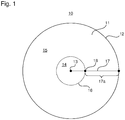
- Fig.1 is a plan view of a group III nitride single crystal substrate 10 (hereinafter may be referred to as "substrate 10") according to one embodiment to explain an inner region and an outer region in a case where a main surface of a substrate has a circular shape.
- the substrate 10 comprises a main surface 11, and the main surface 11 comprises a periphery 12.
- the substrate 10 is a substrate having a circular shape, and the shape of the main surface 11 is circle. Since the shape of the main surface 11 has rotational symmetry, the position of the center 13 of the main surface 11 is the position of the axis of the rotational symmetry.
- the boundary 16 between the inner region 14 and the outer region 15 in the main surface 11 is a concentric circle whose radius is 30% of the radius of the main surface 11.
- Measurement spots of micro-Raman spectra in the outer region 15 are arranged at regular intervals over the entire length of a part 17a of the line segment 17, wherein the line segment 17 connects the center 13 of the main surface 11 and the periphery 12, and wherein the part 17a is a part contained in the outer region 15.
- Fig.2 is a plan view of a group III nitride single crystal substrate 20 (hereinafter may be referred to as "substrate 20") according to one embodiment to explain an inner region and an outer region in a case where a main surface of a substrate has a regular polygonal shape.
- the substrate 20 comprises a main surface 21, and the main surface 21 comprises a periphery 22.
- the substrate 20 is a substrate having a regular hexagonal shape, and the shape of the main surface 21 is regular hexagon. Since the shape of the main surface 21 has rotational symmetry, the position of the center 23 of the main surface 21 is the position of the axis of the rotational symmetry.
- Measurement spots of micro-Raman spectra in the outer region 25 are arranged at regular intervals over the entire length of a part 27a of the line segment 27, wherein the line segment 27 connects the center 23 of the main surface 21 and the periphery 22, and wherein the part 27a is a part contained in the outer region 25.
- Fig.3 is a plan view a group III nitride single crystal substrate 30 (hereinafter may be referred to as "substrate 30") according to one embodiment to explain an inner region and an outer region in a case where a main surface of a substrate has a partly-distorted circular shape.
- the substrate 30 comprises a main surface 31, and the main surface 31 comprises a periphery 32.
- the substrate 30 is a circular substrate having an orientation flat, that is, the substrate 30 is a substrate having a circular shape which is partly cut out, and the shape of the main surface 31 is a partly-distorted circle. Since the shape of the main surface 31 is partly distorted from circle, it does not have rotational symmetry.
- the "original circle” 39 can be found as the circle 39 whose periphery has the longest (total) overlap 39a with the periphery 32 of the main surface 31.
- the center of the main surface 31 is the center 33 of the original circle 39.
- the boundary 36 between an inner region 34 and an outer region 35 is a trace drawn by a point 38 such that a distance from the center 33 to the point 38 is 30% of the distance from the center 33 to the periphery 32: i.e.
- Measurement spots of micro-Raman spectra in the outer region 35 are arranged at regular intervals over the entire length of a part 37a of the line segment 37, wherein the line segment 37 connects the center 33 of the main surface 31 and the periphery 32, and wherein the part 37a is a part contained in the outer region 35.
- Fig.4 is a plan view of a group III nitride single crystal substrate 40 (hereinafter may be referred to as "substrate 40") according to one embodiment to explain an inner region and an outer region in a case where a main surface of a substrate has a partly-distorted regular polygonal shape.
- the substrate 40 comprises a main surface 41, and the main surface 41 comprises a periphery 42.
- the substrate 40 is a regular hexagonal substrate having an orientation flat, that is, the substrate 40 is a substrate having a regular hexagonal shape which is partly cut out, and the shape of the main surface 41 is a partly-distorted regular hexagon. Since the shape of the main surface 41 is partly distorted from regular hexagon, it does not have rotational symmetry.
- the "original regular hexagon” 49 can be found as the regular hexagon 49 whose periphery has the longest (total) overlap 49a with the periphery 42 of the main surface 41.
- the center of the main surface 41 is the center 43 of the original regular hexagon 49.
- the boundary 46 between an inner region 44 and an outer region 45 is a trace drawn by a point 48 such that a distance from the center 43 to the point 48 is 30% of the distance from the center 43 to the periphery 42: i.e.
- Measurement spots of micro-Raman spectra in the outer region 45 are arranged at regular intervals over the entire length of a part 47a of the line segment 47, wherein the line segment 47 connects the center 43 of the main surface 41 and the periphery 42, and wherein the part 47a is a part contained in the outer region 45.
- Smaller "wave number deviation ratio" in the group III nitride single crystal substrate means that the substrate has less crystal defect(s) and is more uniform substrate.
- the "wave number deviation ratio” is preferably within the range of ⁇ 0.05%, more preferably within the range of ⁇ 0.03%.
- Wave numbers of micro-Raman spectra can be evaluated by means of a micro-Raman spectrometer.
- a laser of 531.98 nm in wavelength is employed as an excitation laser; slit width and a grating are adjusted such that wave number resolution of no more than 0.5 cm -1 is obtained; excitation laser power is adjusted to be about 10 mW; and the excitation layer is irradiated to the main surface of a group III nitride single crystal substrate, through an objective lens of 100 times magnification such that the diameter of an measurement spot becomes about 1 ⁇ m, to measure a local Raman spectrum.
- Calibration of measured Raman spectra are carried out by means of, for an example, a wave number of 521.448 cm -1 which is a representative Raman shift of silicon substrates, or the wave number of the excitation laser.
- the peak to be subjected to wave number evaluation in a Raman spectrum of a group III nitride single crystal may be any peak as long as the peak can be observed.
- Raman spectra of wurtzite group III nitrides peaks corresponding to respective modes of A 1 (TO), A 1 (LO), E 1 (TO), E 1 (LO), E 2 high , and E 2 low can be observed.
- Such a peak that corresponds to a lattice vibration mode whose Raman shift wave number changes depending on stress in the in-plane direction of the main surface of a group III nitride single crystal substrate is preferably employed for evaluation.
- the E 2 high peak may be preferably employed.
- the E 2 high peak can be observed by irradiating the excitation laser onto the main surface, irrespective of the face orientation of the growth face (the main surface) of the group III nitride single crystal substrate.
- the wave number of the E 2 high peak changes depending on stress in the in-plane direction of the main surface of the group III nitride single crystal substrate, irrespective of the face orientation of the main surface.
- the E 2 high peak of gallium nitride is observed at 567.6 cm -1
- the E 2 high peak of aluminum nitride is observed at 657.4 cm -1 .
- the group III nitride which constitutes the group III nitride single crystal substrate is not particularly limited.
- the group III nitride single crystal substrate include an AlN substrate, a GaN substrate, an AlGaN substrate, an InGaN substrate, and an InAlGaN substrate.
- the AlN substrate and the GaN substrate are preferable in view of better lattice-matching when a group III nitride semiconductor light emitting device layer is grown over the substrate and in view of higher transparency of light of 210 to 365 nm in wavelength which is deep ultraviolet region.
- the diameter and the thickness of the group III nitride single crystal substrate is not particularly limited, and may be suitably determined depending on desired use.
- the group III nitride single crystal substrate of the present invention can have a large diameter, because the substrate has small residual stress therein.
- the diameter and the thickness of the substrate may be suitably determined, the diameter being preferably 10 to 210 mm, especially preferably 20 to 210 mm, and the thickness being preferably 50 to 2000 ⁇ m, especially preferably 100 to 1000 ⁇ m.
- the face orientation of the growth face (the main surface) of the group III nitride single crystal substrate is not particularly limited, as long as the group III nitride single crystal can grow with the face orientation as the growth face orientation.
- Examples of the face orientation of the growth face (the main surface) of the group III nitride single crystal substrate include +c-face, -c-face, m-face, a-face, and r-face.
- the half width of an X-ray rocking curve measured for a group III nitride single crystal substrate means better crystal quality of the substrate.
- the half width of the X-ray rocking curve measured for (0002) diffraction plane is preferably no more than 100 arcsec, and especially preferably no more than 50 arcsec.
- the half width of the X-ray rocking curve measured for (11-20) diffraction plane is preferably no more than 100 arcsec, and especially preferably no more than 50 arcsec.
- the half width of the X-ray rocking curve measured for (10-10) diffraction plane is preferably no more than 100 arcsec, and especially preferably no more than 50 arcsec.
- the group III nitride single crystal substrate preferably has a silicon concentration of 1 ⁇ 10 15 to 1 ⁇ 10 19 cm -3 , an oxygen concentration of 1 ⁇ 10 15 to 2 ⁇ 10 19 cm -3 , and a carbon concentration of 1 x 10 14 to 5 ⁇ 10 17 cm -3 ; more preferably has a silicon concentration of 2 ⁇ 10 15 to 5 ⁇ 10 18 cm -3 , an oxygen concentration of 2 ⁇ 10 15 to 1 ⁇ 10 19 cm -3 , and a carbon concentration of 2 ⁇ 10 14 to 3 ⁇ 10 17 cm -3 ; and especially preferably has a silicon concentration of 3 ⁇ 10 15 to 2 ⁇ 10 18 cm -3 , an oxygen concentration of 3 ⁇ 10 15 to 2 ⁇ 10 18 cm -3 , and a carbon concentration of 3 ⁇ 10 14 to 1 ⁇ 10 17 cm -3 .
- the group III nitride single crystal substrate does not form a pit (recess) when the substrate is subjected to polishing treatment, a group III nitride semiconductor light emitting device layer can be uniformly grown over the single crystal substrate.
- the yield of the light emitting diode can be improved.
- the group III nitride single crystal substrate is also considered to have improved workability when making the wafer into chips, since distortion which accompanies crystal defects is reduced or eliminated in the substate.
- Such a group III nitride single crystal substrate of the present invention can be produced by the method for producing a group III nitride single crystal substrate of the present invention described later. In the following, the method for producing a group III nitride single crystal substrate of the present invention will be described in detail.
- the method for producing a group III nitride single crystal substrate of the present invention comprises, in the sequence set forth: (a) thermally treating a base substrate at a constant temperature of 1000 to 2300°C for at least 60 seconds, wherein the base substrate is a group III nitride single crystal substrate comprising a main surface; and (b) growing a group III nitride single crystal layer over the main surface by means of vapor phase epitaxy, wherein the main surface has a surface roughness of no more than 0.5 nm in terms of arithmetical mean height Sa.
- a base substrate used for production of a group III nitride singe crystal substrate has distortion remaining therein, and residual stress in the base substrate changes when a group III nitride single crystal layer is grown over the base substrate depending on growth conditions and a thermal history, which results in formation of a spot where stress is concentrated in the proximity of the center of the base substrate.
- stress concentration also occurs in the position of the layer grown over the spot, which results in occurrence of a crystal defect. Peak wave numbers of a micro-Raman spectrum of the grown single crystal layer shift in the position where stress is concentrated. Residual stress in a base substrate thus changes depending on growth conditions and a thermal history.
- Patent Literature 6 teaches carrying out thermal cleaning prior to growing a group III nitride single crystal over a base substrate: in more detail, Patent Literature 6 teaches, when the base substrate is an aluminum nitride substrate or a sapphire substrate, carrying out thermal cleaning to remove organic materials attached on the base substrate by maintaining the base substrate at a temperature of no less than 1000°C and no more than a growth temperature of the group III nitride single crystal for about 10 minutes while supplying a carrier gas containing hydrogen, and then growing the crystal. It is noted, however, such a method cannot suppress occurrence of crystal defects in the proximity of the center of the single crystal layer. The reason thereof is considered as in the following.
- the surface profile of the growth face (the main surface) of the base substrate may change accompanying stress relaxation, and thus flatness of the growth face is lost accompanying stress relaxation even if the growth face is flat enough before the thermal cleaning, and then the single crystal layer is grown over the growth face whose flatness is lost, which results in occurrence of crystal defects during growth of the single crystal layer.
- a base substrate is thermally treated at a constant temperature of 1000 to 2300°C for at least 60 seconds, and thereafter (b) under such a condition that the main surface of the base substrate has sufficiently high flatness (the surface profile is no more than 0.5 nm in terms of arithmetical mean height Sa), a group III nitride single crystal layer is grown over the main surface of the base substrate, which allows uniform crystal growth, which makes it possible to produce a high-quality group III nitride single crystal substrate with reduced occurrence of crystal defect(s) in the proximity of the center of thereof.
- the material of the base substrate is preferably the same kind of material as the group III nitride single crystal layer to be grown over the base substrate.
- Examples of such a base substrate include group III nitride single crystal substrates such as an AlN substrate, a GaN substrate, and an AlGaN substrate.
- group III nitride single crystal substrates such as an AlN substrate, a GaN substrate, and an AlGaN substrate.
- an aluminum nitride single crystal substrate is preferably employed as the base substrate, in view of growing an uniform and thick aluminum nitride single crystal layer.
- Aluminum nitride single crystal substrates produced by known methods such as PVT method and HVPE method may be employed as the aluminum nitride single crystal substrate.
- the base substrate preferably has a small number of defects (e.g. having a dislocation density of no more than 10 6 cm -2 ) and a thickness of 100 to 1000 ⁇ m, and preferably has a high flatness of the crystal growth surface (the main surface): i.e. a surface roughness of the crystal growth surface (the main surface) of no more than 0.5 nm, more preferably no more than 0.3 nm, and further preferably 0.2 nm, in terms of arithmetical mean height (Sa) (ISO 25178).
- the crystal growth surface (the main surface) of the base substrate may be polished such that the surface roughness of the crystal growth surface (the main surface) becomes no more than the upper limit if necessary.
- the surface roughness (arithmetical mean height Sa) of the main surface of the base substrate is a value calculated based on results of observation of a square-shaped field of 2 ⁇ m in length ⁇ 2 ⁇ m in width arranged in the center of the main surface by means of atomic force microscopy (AFM).
- AFM atomic force microscopy
- the diameter of the base substrate is not particularly limited, and may be suitably determined depending on desired use. For example, the diameter may be suitably determined within the range of 10 to 210 mm.
- the face orientation of the base substrate is not particularly limited, and may be suitably determined depending on the face orientation of the group III nitride single crystal layer to be grown. Examples of the face orientation of the main surface of the base substrate include +c-face, -c-face, m-face, a-face, and r-face.
- Impurity concentrations of the base substrate considerably vary depending on the kind of the substrate and the production method of the substrate. Impurity concentrations of the base substrate may be suitably determined depending on desired use.
- impurity concentrations thereof are: preferably 1 ⁇ 10 15 to 2 ⁇ 10 19 cm -3 in silicon concentration, 1 ⁇ 10 15 to 5 ⁇ 10 19 cm -3 in oxygen concentration, and 1 ⁇ 10 14 to 5 ⁇ 10 19 cm -3 in carbon concentration; and especially preferably 2 ⁇ 10 15 to 1 ⁇ 10 19 cm -3 in silicon concentration, 2 ⁇ 10 15 to 2 ⁇ 10 19 cm -3 in oxygen concentration, and 2 ⁇ 10 16 to 1 ⁇ 10 19 cm -3 in carbon concentration.
- impurity concentrations are within the above range, stress strong enough to cause crystal defects does not occur between the base substrate and the group III nitride single crystal layer during growth, and thus defects are not formed in the central part of the substrate, even when there are differences between impurity concentrations of the base substrate and impurity concentrations of the group III nitride single crystal layer grown on the base substrate.
- a ratio of the total concentration of silicon, oxygen, and carbon, which are major impurities in the group III nitride single crystal layer, in the group III nitride single crystal layer , to the total concentration of silicon, oxygen, and carbon, which are major impurities in the base substrate, in the base substrate is preferably 0.001 to 100, more preferably 0.005 to 20, and further preferably 0.01 to 5 (single crystal layer / base substrate).
- the ratio of total impurity concentrations within the above range makes it possible to suppress formation of cracks in the group III nitride single crystal layer due to stress originated from differences in impurity concentrations between the group III nitride single crystal and the base substrate.
- the ratio of the total impurity concentrations of the group III nitride single crystal layer and the base substrate being closer to 1, i.e. smaller concentration difference, reduces a risk of crystal defect formation in the proximity of the center; but the method of the present invention offers reduced crystal defect formation in the proximity of the center even when there is a considerable difference in impurity concentrations between the group III nitride single crystal layer and the base substrate, which means greater possibility for stress originated from the impurity concentration difference to occur.
- the production method of the present invention comprises thermally treating the base substrate for at least 60 seconds at a constant temperature of 1000 to 2300°C (step (a)), prior to growing a group III nitride single crystal layer over the base substrate. Details of the thermal treatment will be described in the following.
- the thermal treatment of the base substrate is carried out so as to make residual stress in the base substrate relax.
- the thermal treatment of the base substrate is carried out by keeping the base substrate at a constant temperature of 1000 to 2300°C for at least 60 seconds.
- a higher temperature is preferred for the temperature of the thermal treatment, and the thermal treatment temperature may be suitably selected within the above temperature range considering a substrate temperature in a growth step (step (b)).
- the thermal treatment temperature may be selected from a range which is within the range of 1000 to 2300°C and which is close to the substrate temperature (growth temperature) in the growth step (step (b)) (preferably within the range of ⁇ 100°C from the growth temperature, more preferably within the range of ⁇ 50°C from the growth temperature).
- an atmosphere gas during the thermal treatment a gas which does not react with the base substrate is preferably used.
- the atmosphere gas one gas may be used alone, or a mixed gas of at least two gases may be used.
- the atmosphere gas during the thermal treatment preferably comprises a halogen gas, a hydrogen halide gas, and/or ammonia gas, and especially preferably comprises a halogen gas and/or a hydrogen halide gas.
- the supply of the atmosphere gas is not particularly limited, and may be determined depending on the volume of a reactor; in general, the supply is, for example, preferably 50 to 50000 sccm, more preferably 100 to 20000 sccm. In the present description, sccm is a unit of mass flow which means flow per 1 minute in terms of volume (cc) at the standard state (0°C, 1 atm). It is preferred to remove impurity gases such as oxygen, water vapor, carbon monoxide, and carbon dioxide, in advance from the gas to be supplied, by means of a gas purifier.
- a time spent for heating (raising the temperature) before the thermal treatment is preferably determined such that stress or cracks do not occur in the base substrate. To be specific, it is preferably 1 minute to 15 hours, and especially preferably 1 minute to 5 hours in view of process efficiency.
- a heating apparatus it is preferred to employ such a production apparatus of a group III nitride single crystal that does not cause damage (such as cracking of the substrate, decomposition of the surface, adhesion of impurities, and contamination by foreign matters) to the base substrate.
- An apparatus which is separate from the production apparatus of the group III nitride single crystal may be employed as the heating apparatus, if the apparatus is composed of members which do not affect the base substrate, such as the apparatus described in the Patent Literature.
- a structure which supports the base substrate is preferably such a structure that there is no position locally abnormally heated in the face of the base substrate. Examples of such a supporting structure include a structure which makes the entire underside surface contact with a susceptor.
- the heating apparatus may be either a continuous-type apparatus or a batch-type apparatus; the batch-type apparatus is more preferable in view of process efficiency.
- a group III nitride single crystal layer is grown by vapor phase epitaxy over the main surface which has a surface roughness (arithmetical mean height Sa) of no more than 0.5 nm (step (b)). If the surface roughness (arithmetical mean height Sa) of the base substrate after the step (a) is no more than 0.5 nm, the step (b) can be carried out on the base substrate as obtained without additional treatment.
- the surface roughness (arithmetical mean height Sa) of the base substrate before the step (a) is no more than 0.5 nm, however, the surface roughness (arithmetical mean height Sa) of the base substrate after the step (a) may become greater than 0.5 nm.
- Plausible causes of such an increase of the surface roughness of the base substrate by experiencing the step (a) include: roughening of the main surface during the thermal treatment, which leads to loss of flatness of the surface; adhesion of foreign matters onto the surface; and a change of the surface profile accompanying relaxation of residual stress of the base substrate.
- the base substrate may be cooled to the ambient temperature and the surface roughness of the main surface of the base substrate may be measured.
- the average rate of the cooling may be, for example, preferably 1 to 170 K/min.
- the step (b) may be carried out without carrying out the planarizing step.
- means to reduce the surface roughness (arithmetical mean height Sa) of the main surface of the base substrate to 0.5 nm or less in the planarizing step include: polishing, washing, and thermal cleaning. Among them, in view of ease of fine surface control, polishing may be preferably employed, and chemomechanical polishing (CMP) may be especially preferably employed. In CMP, known slurries such as silica slurry and alumina slurry may be employed.
- the step (b) may be carried out on the base substrate as obtained without cooling of the substrate and measurement of the surface roughness.
- the surface roughness (arithmetical mean height Sa) of the main surface of the base substrate is a value calculated based on results of observation of a square-shaped field of 2 ⁇ m in length ⁇ 2 ⁇ m in width arranged in the center of the main surface by means of atomic force microscopy (AFM).
- a group III nitride single crystal layer is grown over the main surface of the base substrate after the step (a) by means of vapor phase epitaxy (step (b)), to produce a group III nitride single crystal.
- a known vapor phase growth method may be employed without particular limitation.
- Examples of vapor phase growth methods include sublimation (PVT) method, metalorganic vapor phase epitaxy (MOCVD), and hydride vapor phase epitaxy (HVPE). Among them, PVT or HVPE method is preferred in that they can grow a single crystal of good crystal quality at a high growth rate.
- step (b) will be described in detail, giving examples of HVPE method and PVT method.
- a conventional HVPE apparatus such as a horizontal flow reactor and a vertical perpendicular flow reactor may be employed.
- an apparatus which can supply raw material gases and a carrier gas from the upstream side of the substrate and can exhaust a reaction product gas from the downstream side, can adjust gas supply by means of a mass flow controller, and can heat the base substrate by e.g. high-frequency heating or resistance heating, and whose members are coated with a material which does not react with the raw material gases or the reaction product gas and does not decompose at high temperature, may be preferably used.
- a batch-type apparatus which can grow group III nitride single crystal layers over a plurality of base substrates at the same time may be particularly preferably employed.
- HVPE method is employed as the vapor phase growth method in the step (b), it is preferred to supply a carrier gas into the reactor to form a flow of raw material gases (a group III raw material gas and a nitrogen source gas), so as to the supply raw material gases onto the base substrate in a reactor.
- a carrier gas hydrogen gas and/or various inert gases may be used.
- the carrier gas one gas may be used alone, or a mixed gas of at least two gases may be used. Among them, in view of not disadvantageously affect the production of the group III nitride single crystal, one or more gas selected from hydrogen gas and nitrogen gas is preferably used as the carrier gas.
- the supply of the carrier gas may be suitably determined depending on the volume of the reactor; in general, it is for example preferably 50 to 50000 seem, more preferably 100 to 10000 sccm. It is also preferred to remove impurity gases such as oxygen, water vapor, carbon monoxide, and carbon dioxide from the carrier gas in advance, by means of a gas purifier.
- group III raw material gas a known group III raw material gas used when producing a group III nitride single crystal may be used without particular limitations. Among them, the advantageous effect of the present invention is significant when a group III raw material gas containing aluminum is used.
- an aluminum halide gas such as aluminum chloride gas and aluminum iodide gas is preferably used.
- Aluminum halide gases are preferred as the group III raw material gas used in the present invention because they have high reactivity and offer a high growth rate.
- the aluminum halide gas may be obtained by vaporizing a solid aluminum halide, or may be obtained by reacting metal aluminum with a halogen-based gas for raw material formation such as hydrogen chloride gas and chloride gas.
- a halogen-based gas for raw material formation such as hydrogen chloride gas and chloride gas.
- a solid of 99,99% or more in purity is preferably used as aluminum as the raw material of the aluminum halide gas.
- the dimensions and shape of the solid aluminum is not particularly limited; in view of contact efficiency of aluminum and the halogen-based gas for raw material formation and a flow path resistance of the halogen-based gas, a pellet-shape of 0.1 to 10 mm in diameter and 0.1 to 10 mm in length may be preferably used.
- the aluminum halide gas may be obtained by a reaction of a metal-organic gas containing aluminum and a halogen-based gas for raw material formation.
- the group III raw material gas is preferably supplied onto the base substrate together with the carrier gas.
- the concentration of the group III raw material gas in a mixed gas of the group III raw material gas and the carrier gas may be, for example, 0.0001 to 10% by volume.
- the supply of the group III raw material gas may be, for example, 0.005 to 500 sccm.
- a nitrogen source gas is suppled onto the base substrate.
- a reactive gas containing nitrogen may be employed; in view of cost and ease of handling, ammonia gas is preferably used.
- the nitrogen source gas is supplied on the base substrate, usually as suitably diluted in the carrier gas.
- the supply of the nitrogen source gas and the supply of the carrier gas may be determined depending on e.g. volume of the reactor.
- the supply of the carrier gas is preferably 50 to 10000 sccm, and more preferably 100 to 5000 sccm.
- the concentration of the nitrogen source gas in a mixed gas of the nitrogen source gas and the carrier gas may be, for example, 0.001 to 10% by volume.
- the supply of the nitrogen source gas is preferably 0.01 to 1000 sccm.
- the reaction of the group III raw material gas and the nitrogen source gas may also be conducted in the presence of at least one halogen-based gas selected from hydrogen halide gases and halogen gases.
- the halogen gas include chlorine gas and bromine gas.
- the hydrogen halide gas include hydrogen chloride gas and hydrogen bromide gas.
- hydrogen halide gas is preferably used as the halogen-based gas, in view of low corrosiveness against gas conduits, ease of handling, and cost. So as to obtain a group III nitride single crystal of higher quality, it is preferred to supply as the group III raw material gas a mixed gas obtained by further mixing the aluminum halide gas with an additional halogen-based gas, as described in Patent Literature 4.
- a barrier gas may be supplied from a gap between a nozzle supplying the group III raw material gas and a nozzle supplying the nitrogen source gas, so as to control mixing of the group III raw material gas and the nitrogen source gas, as described in Patent Literature 6.
- the temperature of the base substrate during crystal growth (growth temperature)
- a conventional growth temperature may be employed without particular limitation.
- the growth temperature is preferably 1000 to 1700°C.
- the temperature of the base substrate (growth temperature) is preferably 1200 to 1600°C.
- the supply of the aluminum halide gas is preferably 0.001 to 100 sccm.
- HVPE method growth of a group III nitride single crystal layer is begun by supplying both a group III raw material gas and a nitrogen source gas are supplied onto a heated base substrate.
- the order of beginning supply of the group III raw material gas, the nitrogen source gas, and the halogen-based gas onto the base substrate is not particularly limited.
- Supply of gases may be begun, for example, in the sequence set forth: (i) the halogen-based gas, the nitrogen source gas, and the group II raw material gas; (ii) the nitrogen source gas, the halogen-based gas, and the group III raw material gas; (iii) the halogen-based gas, the group III raw material gas, and the nitrogen source gas; (iv) the group III raw material gas, the halogen-based gas, and the nitrogen source gas; (v) the nitrogen source gas, the group III raw material gas, and the halogen-based gas; or (vi) the group III raw material gas, the nitrogen source gas, and the halogen-based gas.
- two or three gases selected from the group III raw material gas, the nitrogen source gas, and the halogen-based gas may be mixed and supplied as a mixed gas.
- supply of two or three gases selected from the group III raw material gas, the nitrogen source gas, and the halogen-based gas may be begun at the same time from separate gas supply pipes.
- the growth rate of the aluminum-based group III nitride single crystal layer becomes 10 ⁇ m/h or more, more preferably 15 ⁇ m/h or more.
- the upper limit of the growth rate is not particularly limited, it may be for example 300 ⁇ m/h or less in view of improving crystal quality.
- the thickness of the group III nitride single crystal layer to be grown is not particularly limited, and it may be suitably determined depending on desired use of the group III nitride single crystal substrate to be produced. It is usually 50 to 2000 ⁇ m.
- the pressure in the reactor may be suitably determined depending on e.g. raw materials used. During growth of the group III nitride single crystal, the pressure in the reactor is preferably 0.2 to 1.5 atm.
- Cooling of the group III nitride single crystal after growth is preferably carried out at such a rate that stress or a crack does not occur in the base substrate.
- the time spent for the cooling is preferably 10 minutes to 15 hours, and preferably 30 minutes to 6 hours in view of process efficiency.
- the group III nitride single crystal layer may be grown by PVT method.
- Conventional conditions may be employed for crystal growth conditions of PVT method.
- materials employable as the material of a crucible used in PVT method include: metals such as tungsten, tantalum, and zirconium; carbides thereof such as tungsten carbide and tantalum carbide; graphite; aluminum nitride; and boron nitride.
- a common crucible comprises a cylindrical outer shape, and a base substrate is arranged on one side of the inside of the crucible on one hand, and a group III nitride raw material is arranged on the opposite side of the inside of the crucible on the other hand.
- group III nitride raw material a group III nitride powder or a sintered group III nitride may be used.
- the group nitride powder or the sintered group III nitride is heated at 1800 to 2500°C to reduce impurities such as oxygen, silicon, and carbon in advance, and thus obtained group III nitride with reduced impurities is preferably used as the raw material.
- the group III nitride raw material may be obtained by reacting a group III metal of high purity with a nitrogen source gas such as nitrogen gas or ammonia gas at a temperature equal to or greater than the melting point of the metal.
- a PVT reactor in one embodiment, comprises a water-cooled quartz double tube structure comprising a inner tube and an outer tube, and the crucible is arranged inside the inner tube of the quartz double tube.
- the inside of the PVT reactor has a structure such that an inert gas such as nitrogen gas, argon gas, and helium gas can be supplied, and nitrogen gas alone or a mixed gas comprising nitrogen gas is supplied when growing a group III nitride single crystal layer.
- the PVT reactor comprises an exhaust system which is connected to a vacuum pump such that oxidizing components such as oxygen gas and water in the system can be efficiently exhausted.
- the pressure in the reactor may be suitably adjusted within the range of 1 to 1000 Torr.
- a halogen-based gas such as hydrogen chloride gas and chlorine gas may be supplied into the PVT reactor. It is possible to facilitate removal of e.g. impurities, deposits of the group III nitride, and foreign matters in the reactor, as well as to control a driving force of deposition of the group III nitride single crystal, by supplying the halogen-based gas suitably in an amount of 0.01 to 10% by volume on the basis of the total gas volume in the reactor while heating the inside of the reactor.
- the crucible may be heated by high-frequency heating or resistive heating.
- high-frequency heating (a) a high-frequency wave may be directly applied to the crucible, or (b) a heatable part to which the high-frequency wave can be applied may be provided around the outside of the crucible, and the crucible may be indirectly heated by making a heat generated in the heatable part be transferred to the crucible.
- One heating method of them may be employed alone, or both of them may be employed in combination.
- Inside the crucible e.g. a tapered structure, a protrusion structure, a hollow structure, or a curved structure may be suitably provided such that a temperature distribution suitable for deposition of the group III nitride single crystal substrate is realized.
- the group III nitride single crystal layer can be grown over the base substrate by: heating the group III nitride raw material at 1800 to 2500°C, to decompose the group III nitride raw material into a group III nitride raw material gas; making the group III nitride raw material gas diffuse and be transported to the base substrate; and making the group III nitride deposit from the group III nitride raw material gas onto the base substrate.
- the temperature of the base substrate (growth temperature) is suitably selected from the range which is within the range of 1600 to 2300°C and is equal to or lower than the heating temperature of the group III nitride raw material.
- the substrate is maintained at the growth temperature until a desired film thickness is obtained, to grow the group III nitride single crystal layer. Thereafter the substrate is cooled to the room temperature at a cooling rate of 1 to 1000 K/h, and then a layered body comprising the base substrate and the group III nitride single crystal layer is taken out from the reactor.
- the obtained group III nitride single crystal substrate may be preferably used for fabrication of electronic devices comprising an aluminum-based group III nitride (mainly aluminum gallium nitride mixed crystal) semiconductor, such as light emitting devices, Schottky barrier diodes, and high electron mobility transistors.
- the obtained group III nitride single crystal substrate may be subjected to grinding, and then to planarization of the surface by grinding, and thereafter to chemomechanical polishing (CMP) to remove a damaged layer formed by the grinding of the surface, to give a group III nitride single crystal substrate having a flat surface.
- CMP chemomechanical polishing
- a new group III nitride single crystal substrate consisting of the group III nitride single crystal layer grown over the base substrate may be obtained by removing the base substrate by a conventional process method such as mechanical cutting, laser cutting, or grinding. Grinding and chemomechanical polishing (CMP) may be carried out by conventional methods.
- An abrasive comprising a material such as silica, alumina, ceria, boron carbide, boron nitride, and diamond may be used.
- the nature of the abrasive may be any of alkaline, neutral, and acidic.
- a weak alkaline, neutral or acidic abrasive is preferably used rather than a strong alkaline abrasive, since nitrogen face (-c-face) of aluminum nitride has low alkaline resistance: to be specific, an abrasive of 9 or less in pH is preferably used.
- an additive such as an oxidant may be added so as to increase polishing rate.
- a commercially available polishing pat may be used, and its material and hardness is not particularly limited.
- Obtained group III nitride single crystal substrates were evaluated by Nomarski differential interference contrast microscopy, observation by X-ray reflection topography, measurement of impurity concentrations, measurement of surface roughness (flatness), measurement of micro-Raman spectra, and observation by white-light interference microscopy. Details of evaluation methods are as in the following.
- a group III nitride single crystal substrate was observed in a bright field with a magnification of 100 to 500 times, by means of a Nomarski differential interference contrast microscope (LV150 manufactured by Nikon Corporation).
- a high-resolution thin film X-ray diffractometer (X'Pert Pro MRD manufactured by PANalytical B.V.) was used. From a Cu-target X-ray tube, characteristic X-ray (direct beam intensity: 40000 cps) was generated under the conditions of 45 kV of acceleration voltage and 40 mA of filament current, whereby X-ray beam was taken out by line focus. The generated X-ray beam was reflected by an X-ray mirror module (Goebel mirror) to give a horizontal X-ray beam of high intensity.
- X'Pert Pro MRD manufactured by PANalytical B.V.
- the X-ray mirror module was equipped with a 1/2° divergence slit (lateral limitation slit) and a vertical limitation slit of 50 ⁇ m in width, the both being arranged at the entrance of the X-ray mirror module, to make the X-ray beam narrowed to approximately 1.2 mm in beam width.
- the X-ray beam was irradiated onto an aluminum nitride substrate arranged on a measurement stage.
- the CuK ⁇ 1 ray diffracted from (114) plane of the aluminum nitride single crystal substrate was detected by a two-dimensional semiconductor X-ray detector (PIXcel 3D semiconductor detector manufactured by PANalytical B.V.), whereby an X-ray reflection topography image was acquired. Image analysis of the acquired X-ray reflection topography image was carried out.
- PIXcel 3D semiconductor detector manufactured by PANalytical B.V.
- concentrations of silicon atoms, oxygen atoms, and carbon atoms were determined by secondary ion mass spectrometry (IMS-f6 manufactured by CAMECA Instruments Inc.) using cesium ion (acceleration voltage: 15 kV) as the primary ion. Secondary ion intensities at an analysis depth of 2 ⁇ m from the surface were measured, and silicon concentration, oxygen concentration, and carbon concentration were determined based on a calibration curve which had been separately prepared using an AlN standard sample.
- Wave numbers of micro-Raman spectra were evaluated by means of NRD-7100 micro-Raman spectrometer manufactured by JASCO Corporation.
- a laser of 531.98 nm in wavelength was used as an excitation laser.
- a slit of 10 ⁇ m in width ⁇ 1000 ⁇ m in length, and a grating of 600 lines/mm were used.
- the excitation laser (output power: 10.8 mW) was concentrated through an objective lens of 100 times magnification such that the diameter of a measurement spot became about 1 ⁇ m, and was irradiated to a group III nitride single crystal, to acquire a local Raman spectrum.
- Three spectra each acquired with an exposure time of 5 seconds were integrated.
- Wave numbers of measured Raman spectra were calibrated based on a Raman shift of 521.448 cm -1 in wave number which was a Raman shift of a silicon substrate measured under the same conditions.
- E 2 high Raman shift peaks of measured group III nitride single crystals were fitted with Lorentzian functions to give peak wave numbers thereof.
- Measurement spots in the inner region were: when one or more bright spot(s) was/were observed in the X-ray reflection topography image, micro-Raman spectra were measured for at least 3 spots in the inner region, the at least 3 spots including all of the bright spot(s); when no bright spot was observed in the X-ray reflection topography image, micro-Raman spectra were measured for the center of the main surface and at least 2 spots randomly selected from the inner region (i.e. at least 3 spots in total).
- Measurement spots of micro-Raman spectra in the outer region were at least 3 spots arranged at regular intervals (2 mm) along the entire length of a part of a line segment, the line segment connecting the center of the main surface and the periphery, and the part being included in the outer region.
- the ratio of the difference between the minimum value of peak wave numbers of micro-Raman spectra in the inner region (v A ) and the average value of peak wave numbers of micro-Raman spectra in the outer region (v B ) to the average value of peak wave numbers of micro-Raman spectra in the outer region (v B ) was calculated by the following formula. 100 ⁇ ⁇ A ⁇ ⁇ B / ⁇ B %
- the base substrate had a silicon concentration of 5 ⁇ 10 18 cm -3 , an oxygen concentration of 7 ⁇ 10 18 cm -3 , and a carbon concentration of 8 ⁇ 10 18 cm -3 .
- the base substrate was subjected to ultrasonic cleaning with acetone and isopropyl alcohol. After the ultrasonic cleaning of the base substrate, the base substrate was placed on a susceptor made of BN-coated graphite in a HVPE apparatus.
- the pressure in the HVPE apparatus was changed to 0.99 atm.
- the base substrate was heated from the room temperature to 1475°C in 20 minutes, while supplying 3512 sccm of nitrogen gas, 6848 sccm of hydrogen gas, and 10 sccm of ammonia gas onto the base substrate. After 4 minutes and 30 seconds of keeping under the same conditions, the base substrate was cooled to the room temperature and was taken out from the apparatus.
- the surface roughness (arithmetical mean height Sa) of the main surface (Al-face) of the base substrate at this time was 0.6 nm.
- the surface (Al-face) of the base substrate after the thermal treatment was subjected to grinding by #170 to #3000, and then to chemomechanical polishing (CMP).
- the base substrate after polishing was 465 ⁇ m in thickness and 0.08 nm in surface roughness (arithmetical mean height Sa).
- the base substate was washed in the same manner as in the pretreatment, and then was placed on the susceptor made of BN-coated graphite in the HVPE apparatus.
- a hydrogen-nitrogen mixed carrier gas of hydrogen gas and nitrogen gas mixed in a flow rate ratio (sccm / seem) of 8:2 was used, and its total amount of flow was 6500 seem.
- the pressure in the reactor was kept at 0.99 atm during growth. Thereafter the base substrate was heated at 1475°C.
- the wave number deviation ratio of the peak wave number of the micro-Raman spectra of thus obtained aluminum nitride single crystal substrate was measured to be -0.03%. No hillock was observed in the inner region by Nomarski differential interference contrast microscopy. No bright spot was observed in the inner region in an X-ray reflection topography image of the aluminum nitride single crystal layer.
- the surface (Al-face) of the obtained aluminum nitride single crystal substrate was processed in the same manner as in the process of the base substrate.
- the back face (N-face of the base substrate) was mirror-finished by planarizing by grinding and CMP polishing. No pit was observed in white-light interference microscope observation of the aluminum nitride single crystal substrate after the process.
- the aluminum nitride single crystal layer of the obtained group III nitride single crystal substrate had a silicon concentration of 1.3 ⁇ 10 17 cm -3 , an oxygen concentration of 5.5 ⁇ 10 17 cm -3 , and a carbon concentration of 8 ⁇ 10 15 cm -3 .
- the ratio of the total concentration of silicon, oxygen, and carbon in the obtained aluminum nitride single crystal layer to the total concentration (6.9 ⁇ 10 17 cm -3 ) of silicon, oxygen, and carbon in the base substrate was 0.03.
- Example 8 in the inner region of the substrate were observed a hillock by Nomarski differential interference contrast microscopy and a bright spot by image analysis of an X-ray reflection topography image respectively, although they were very small in size. In Example 8, peak wave numbers of micro-Raman spectra showed the lowest value in the center of the substrate, and no pit was observed after polishing.
- Comparative examples 1 to 5 were observed a hillock by Nomarski differential interference contrast microscopy and a bright spot by image analysis of an X-ray reflection topography image respectively, both in the same position (i.e. central defect part) in the inner region of the substrate. Peak wave numbers of micro-Raman spectra showed the lowest value in the central defect part. After polishing, a pit was observed in the central defect part where the hillock and the bright spot had been observed.
- An aluminum nitride single crystal substrate of 50.8 mm in diameter and 580 ⁇ m in thickness prepared by PVT method was used as a base substrate.
- the base substrate was washed in the same manner as in Example 1. Then the base substrate was placed on a susceptor made of BN-coated graphite in a thermal treatment apparatus, such that Al-face of the substrate was in an upward direction. While maintaining the pressure in the thermal treatment apparatus at 1.2 atm, 5000 sccm of nitrogen gas was supplied into the thermal treatment apparatus on one hand, and the base substrate was heated to 1800°C in 20 minutes on the other hand. After 20 minutes of keeping under the same conditions, the base substrate was cooled in 30 minutes, and the base substrate was taken out from the apparatus.
- the surface roughness (arithmetical mean height Sa) of the main surface (Al-face) of the base substrate was measured to be 0.62 nm.
- the main surface (Al-face) of the base substrate was subjected to chemomechanical polishing (CMP), to make the surface roughness (arithmetical mean height Sa) of the main surface 0.15 nm.
- CMP chemomechanical polishing
- the base substrate was placed in a crucible made of tungsten on one hand, and an aluminum nitride raw material was placed in the crucible in the position opposite from the base substrate on the other hand.
- the aluminum nitride raw material had been thermally treated at 2200°C to reduce impurities in advance. That is, the base substrate and the group III nitride raw material were placed in opposite positions in the single crucible.
- the tungsten crucible was placed in a PVT reactor comprising a water-cooled quartz double tube.
- the pressure in the system was reduced to 5 Torr or less, and then nitrogen gas whose dew point was controlled to be -110°C or less was filled in the system, to make the pressure in the system be 760 Torr.
- the pressure in the system was controlled to be constant at 800 Torr by means of a pressure controller.
- heating was begun by applying a high-frequency wave to the tungsten crucible by means of a high-frequency induction heating apparatus.
- the temperature of the base substrate was ramped to 1850°C while maintaining the temperature of the aluminum nitride raw material lower than the temperature of the base substrate by 50°C, and thereafter the temperature of the aluminum nitride raw material was ramped to 2100°C in 1 hour while maintaining the temperature of the base substrate at 1850°C, to promote decomposition of the aluminum nitride raw material on one hand and begin growth of an aluminum nitride single crystal layer over the base substrate on the other hand.
- an aluminum nitride single crystal layer of 56 mm in largest diameter and 8 mm in thickness was grown over the base substrate.
- Impurity concentrations of the base substrate were measured by secondary ion mass spectrometry to be: 6 ⁇ 10 18 cm -3 in silicon concentration, 1 ⁇ 10 19 cm -3 in oxygen concentration, and 1 ⁇ 10 19 cm -3 in carbon concentration, which meant that the total concentration of major impurities were 2.6 ⁇ 10 19 cm -3 .
- Impurity concentrations of the obtained aluminum nitride single crystal layer was measured in the same manner to be: 1 ⁇ 10 17 cm -3 in silicon concentration, 2 x 10 17 cm -3 in oxygen concentration, and 8 ⁇ 10 16 cm -3 in carbon concentration, which meant that the total concentration of major impurities were 3.8 ⁇ 10 17 cm -3 .
- the ratio of the total impurity concentrations of the base substrate and the group III nitride single crystal layer was 0.02.
- a very low hillock was observed in the obtained aluminum nitride single crystal layer by Nomarski differential interference contrast microscopy, in a position distant from the center of the substrate by 2.8 mm (11.0% of the distance from the center to the periphery).
- a bright spot was observed by image analysis of an X-ray reflection topography image of (114) diffraction plane of the aluminum nitride single crystal, in the same position as the hillock observed by Nomarski differential interference contrast microscopy, but the bright spot was obscure.
- the wave number deviation ratio of the E 2 high peak in micro-Raman spectra of the aluminum nitride single crystal layer was analyzed to be -0.03%. No pit was observed after polishing.
- a group III nitride single crystal substrate was produced in the same manner as in Example 14.
- a hillock was observed in the obtained aluminum nitride single crystal layer by Nomarski differential interference contrast microscopy, in a position distant from the center of the substrate by 1.5 mm (6% of the distance from the center to the periphery).
- a clear bright spot was observed by image analysis of an X-ray reflection topography image acquired for (114) diffraction plane of the entire face of the aluminum nitride single crystal, in the same position as the hillock observed by Nomarski differential interference contrast microscopy.
- the wave number deviation ratio of the E 2 high peak in micro-Raman spectra of the aluminum nitride single crystal layer was evaluated to be -0.29%. After polishing, a pit was observed in the central defect part at which the hillock and the bright spot had been observed.
Landscapes
- Chemical & Material Sciences (AREA)
- Engineering & Computer Science (AREA)
- Materials Engineering (AREA)
- Metallurgy (AREA)
- Organic Chemistry (AREA)
- Chemical Kinetics & Catalysis (AREA)
- General Chemical & Material Sciences (AREA)
- Mechanical Engineering (AREA)
- Crystallography & Structural Chemistry (AREA)
- Inorganic Chemistry (AREA)
- Crystals, And After-Treatments Of Crystals (AREA)
- Chemical Vapour Deposition (AREA)
Applications Claiming Priority (2)
| Application Number | Priority Date | Filing Date | Title |
|---|---|---|---|
| JP2017182967 | 2017-09-22 | ||
| PCT/JP2018/035204 WO2019059381A1 (fr) | 2017-09-22 | 2018-09-21 | Substrat monocristallin de nitrure du groupe iii |
Publications (3)
| Publication Number | Publication Date |
|---|---|
| EP3686323A1 true EP3686323A1 (fr) | 2020-07-29 |
| EP3686323A4 EP3686323A4 (fr) | 2021-07-28 |
| EP3686323B1 EP3686323B1 (fr) | 2024-07-31 |
Family
ID=65811394
Family Applications (1)
| Application Number | Title | Priority Date | Filing Date |
|---|---|---|---|
| EP18857897.5A Active EP3686323B1 (fr) | 2017-09-22 | 2018-09-21 | Substrat monocristallin de nitrure du groupe iii |
Country Status (6)
| Country | Link |
|---|---|
| US (2) | US11767612B2 (fr) |
| EP (1) | EP3686323B1 (fr) |
| JP (1) | JP7107951B2 (fr) |
| KR (1) | KR102667614B1 (fr) |
| CN (1) | CN111164242B (fr) |
| WO (1) | WO2019059381A1 (fr) |
Families Citing this family (9)
| Publication number | Priority date | Publication date | Assignee | Title |
|---|---|---|---|---|
| WO2020158254A1 (fr) * | 2019-01-30 | 2020-08-06 | パナソニックセミコンダクターソリューションズ株式会社 | Élément électroluminescent à semi-conducteur |
| JP7262027B2 (ja) * | 2019-05-17 | 2023-04-21 | パナソニックIpマネジメント株式会社 | Iii族窒化物半導体の製造方法 |
| WO2021111835A1 (fr) * | 2019-12-02 | 2021-06-10 | 住友電気工業株式会社 | Substrat en carbure de silicium et procédé de fabrication de substrat en carbure de silicium |
| CN112593293A (zh) * | 2020-11-04 | 2021-04-02 | 奥趋光电技术(杭州)有限公司 | 一种氮化铝晶片热处理方法 |
| WO2023026924A1 (fr) * | 2021-08-23 | 2023-03-02 | 株式会社トクヤマ | Procédé de nettoyage et procédé de production de substrat monocristallin de nitrure du groupe iii |
| JP2023105952A (ja) * | 2022-01-20 | 2023-08-01 | スタンレー電気株式会社 | 単結晶AlN基板、単結晶AlN基板を用いた半導体ウェハ、及びこれらの製造方法 |
| KR102886179B1 (ko) * | 2022-02-24 | 2025-11-14 | 고쿠리츠다이가쿠호진 도호쿠다이가쿠 | AlN 단결정의 제조 방법, AlN 단결정, 및 AlN 단결정 제조 장치 |
| JP7822460B2 (ja) * | 2022-03-24 | 2026-03-02 | 日本碍子株式会社 | AlN単結晶基板及びデバイス |
| JP2023155935A (ja) * | 2022-04-12 | 2023-10-24 | 国立大学法人京都大学 | 発振器、増幅器 |
Family Cites Families (43)
| Publication number | Priority date | Publication date | Assignee | Title |
|---|---|---|---|---|
| JPS6070297U (ja) | 1983-10-20 | 1985-05-18 | 吉野 佐知子 | 物干兼物掛具 |
| EP0970932A1 (fr) * | 1998-07-10 | 2000-01-12 | Sumitomo Electric Industries, Ltd. | Support ceramique |
| JP3836697B2 (ja) * | 2000-12-07 | 2006-10-25 | 日本碍子株式会社 | 半導体素子 |
| JP2003327497A (ja) | 2002-05-13 | 2003-11-19 | Sumitomo Electric Ind Ltd | GaN単結晶基板、窒化物系半導体エピタキシャル基板、窒化物系半導体素子及びその製造方法 |
| JP4052150B2 (ja) * | 2003-03-05 | 2008-02-27 | 住友電気工業株式会社 | 窒化物系半導体装置の製造方法 |
| JP2006032911A (ja) * | 2004-06-15 | 2006-02-02 | Ngk Insulators Ltd | 半導体積層構造、半導体素子およびhemt素子 |
| JP4712450B2 (ja) * | 2004-06-29 | 2011-06-29 | 日本碍子株式会社 | AlN結晶の表面平坦性改善方法 |
| JP4969860B2 (ja) | 2005-04-22 | 2012-07-04 | 国立大学法人三重大学 | AlN単結晶膜の作製方法 |
| US8771552B2 (en) * | 2005-06-23 | 2014-07-08 | Sumitomo Electric Industries, Ltd. | Group III nitride crystal substrate, epilayer-containing group III nitride crystal substrate, semiconductor device and method of manufacturing the same |
| JP2009536605A (ja) | 2006-05-08 | 2009-10-15 | ザ リージェンツ オブ ザ ユニバーシティ オブ カリフォルニア | アルミニウムを含むiii族窒化物半導体化合物の成長方法及び材料。 |
| JP4872450B2 (ja) * | 2006-05-12 | 2012-02-08 | 日立電線株式会社 | 窒化物半導体発光素子 |
| DE102007010286B4 (de) * | 2007-03-02 | 2013-09-05 | Freiberger Compound Materials Gmbh | Verfahren zum Herstellen eines Verbindungshalbleiterwerkstoffs, einer III-N-Schicht oder eines III-N-Bulkkristalls, Reaktor zur Herstellung des Verbindungshalbleiterwerkstoffs, Verbindungshalbleiterwerkstoff, III-N-Bulkkristall und III-N-Kristallschicht |
| JP5079361B2 (ja) * | 2007-03-23 | 2012-11-21 | 日本碍子株式会社 | AlGaN結晶層の形成方法 |
| WO2009011407A1 (fr) * | 2007-07-13 | 2009-01-22 | Ngk Insulators, Ltd. | Procédé de fabrication d'un monocristal de nitrure du groupe iii |
| JP5493861B2 (ja) | 2007-10-09 | 2014-05-14 | 株式会社リコー | Iii族窒化物結晶基板の製造方法 |
| JP2009283785A (ja) * | 2008-05-23 | 2009-12-03 | Showa Denko Kk | Iii族窒化物半導体積層構造体およびその製造方法 |
| JP2010040867A (ja) * | 2008-08-06 | 2010-02-18 | Showa Denko Kk | Iii族窒化物半導体積層構造体およびその製造方法 |
| WO2010092972A1 (fr) * | 2009-02-13 | 2010-08-19 | 電気化学工業株式会社 | Substrat composite pour élément électroluminescent à del, son procédé de fabrication et élément électroluminescent à del |
| CN101958236B (zh) * | 2009-07-20 | 2012-12-19 | 上海半导体照明工程技术研究中心 | 一种半导体衬底及其制备方法 |
| JP2012124473A (ja) * | 2010-11-15 | 2012-06-28 | Ngk Insulators Ltd | 複合基板及び複合基板の製造方法 |
| CN102749316A (zh) * | 2011-04-21 | 2012-10-24 | 中国科学院金属研究所 | 测量SiCf/Ti基复合材料界面微观残余应力的方法 |
| US8778783B2 (en) * | 2011-05-20 | 2014-07-15 | Applied Materials, Inc. | Methods for improved growth of group III nitride buffer layers |
| JP5189712B2 (ja) * | 2011-07-14 | 2013-04-24 | 株式会社アライドマテリアル | AlN基板およびその製造方法 |
| JP5904470B2 (ja) | 2011-12-22 | 2016-04-13 | 国立大学法人東京農工大学 | 窒化アルミニウム単結晶基板、およびこれらの製造方法 |
| KR20130094058A (ko) | 2012-02-15 | 2013-08-23 | 주식회사 케이티 | 커뮤니케이션 시스템, 장치 및 기록 매체 |
| JP2013239474A (ja) * | 2012-05-11 | 2013-11-28 | Sanken Electric Co Ltd | エピタキシャル基板、半導体装置及び半導体装置の製造方法 |
| US9840790B2 (en) | 2012-08-23 | 2017-12-12 | Hexatech, Inc. | Highly transparent aluminum nitride single crystalline layers and devices made therefrom |
| JP6049361B2 (ja) | 2012-09-03 | 2016-12-21 | 東海工業ミシン株式会社 | ミシン |
| JP6328557B2 (ja) * | 2012-09-11 | 2018-05-23 | 株式会社トクヤマ | 窒化アルミニウム基板およびiii族窒化物積層体 |
| JP6070297B2 (ja) | 2013-03-08 | 2017-02-01 | 三菱化学株式会社 | 周期表第13族金属窒化物半導体結晶の製造方法 |
| JP6344688B2 (ja) | 2013-06-10 | 2018-06-20 | 株式会社トクヤマ | アルミニウム系iii族窒化物単結晶の製造方法 |
| JP6108980B2 (ja) | 2013-06-27 | 2017-04-05 | 京セラ株式会社 | 移動通信システム及びユーザ端末 |
| WO2015012005A1 (fr) * | 2013-07-25 | 2015-01-29 | 日本碍子株式会社 | Carte composite et son procédé de fabrication |
| JP6298057B2 (ja) * | 2013-07-26 | 2018-03-20 | スタンレー電気株式会社 | ベース基板の前処理方法、および該前処理を行ったベース基板を用いた積層体の製造方法 |
| JP2015044707A (ja) * | 2013-08-28 | 2015-03-12 | 住友電気工業株式会社 | 窒化ガリウム基板および半導体デバイス |
| US9627197B2 (en) * | 2014-04-15 | 2017-04-18 | Globalwafers Co., Ltd. | Composite substrate, semiconductor device including the same, and method of manufacturing the same |
| JP6405767B2 (ja) | 2014-07-24 | 2018-10-17 | 住友電気工業株式会社 | 窒化ガリウム基板 |
| CN106605291B (zh) * | 2014-09-11 | 2020-05-05 | 株式会社德山 | 氮化铝单结晶基板的洗净方法及层叠体 |
| TWI690632B (zh) | 2014-11-10 | 2020-04-11 | 日商德山股份有限公司 | Iii族氮化物單結晶製造裝置、使用該裝置之iii族氮化物單結晶之製造方法、及氮化鋁單結晶 |
| KR20160076270A (ko) | 2014-12-22 | 2016-06-30 | 현대모비스 주식회사 | 차량용 멀티 코어 시스템 |
| JP6765185B2 (ja) | 2015-05-18 | 2020-10-07 | 株式会社トクヤマ | Iii族窒化物単結晶の製造方法 |
| JP6868364B2 (ja) * | 2015-09-30 | 2021-05-12 | Hoya株式会社 | ガラスブランクおよび磁気ディスク用ガラス基板の製造方法 |
| KR102299465B1 (ko) * | 2017-03-24 | 2021-09-07 | 위스콘신 얼럼나이 리서어치 화운데이션 | 다층 p형 접촉자를 갖는 III-V족 질화물계 발광 소자 |
-
2018
- 2018-09-21 WO PCT/JP2018/035204 patent/WO2019059381A1/fr not_active Ceased
- 2018-09-21 KR KR1020207002168A patent/KR102667614B1/ko active Active
- 2018-09-21 EP EP18857897.5A patent/EP3686323B1/fr active Active
- 2018-09-21 JP JP2019543746A patent/JP7107951B2/ja active Active
- 2018-09-21 US US16/649,382 patent/US11767612B2/en active Active
- 2018-09-21 CN CN201880061317.2A patent/CN111164242B/zh active Active
-
2023
- 2023-08-15 US US18/450,161 patent/US20230407521A1/en not_active Abandoned
Also Published As
| Publication number | Publication date |
|---|---|
| CN111164242B (zh) | 2022-06-24 |
| KR20200056378A (ko) | 2020-05-22 |
| US20200299862A1 (en) | 2020-09-24 |
| US11767612B2 (en) | 2023-09-26 |
| KR102667614B1 (ko) | 2024-05-22 |
| JPWO2019059381A1 (ja) | 2020-09-10 |
| JP7107951B2 (ja) | 2022-07-27 |
| EP3686323A4 (fr) | 2021-07-28 |
| EP3686323B1 (fr) | 2024-07-31 |
| CN111164242A (zh) | 2020-05-15 |
| US20230407521A1 (en) | 2023-12-21 |
| WO2019059381A1 (fr) | 2019-03-28 |
Similar Documents
| Publication | Publication Date | Title |
|---|---|---|
| US20230407521A1 (en) | Group iii nitride single crystal substrate | |
| JP6042545B2 (ja) | 高透明性窒化アルミニウム単結晶層、及びこれからなる素子 | |
| JP2654232B2 (ja) | 高圧相物質単結晶の製造方法 | |
| EP2796596B1 (fr) | Substrat de nitrure d'aluminium monocristallin et procédé de sa production | |
| US20110018104A1 (en) | METHOD FOR PRODUCING A LAMINATED BODY HAVING Al-BASED GROUP-III NITRIDE SINGLE CRYSTAL LAYER, LAMINATED BODY PRODUCED BY THE METHOD, METHOD FOR PRODUCING Al-BASED GROUP-III NITRIDE SINGLE CRYSTAL SUBSTRATE EMPLOYING THE LAMINATED BODY, AND ALUMINUM NITRIDE SINGLE CRYSTAL SUBSTRATE | |
| EP3219833B1 (fr) | Dispositif de fabrication de monocristal de nitrure d'élément du groupe iii, procédé de fabrication de monocristal de nitrure d'élément du groupe iii utilisant celui-ci et monocristal de nitrure d'aluminium | |
| JP7023837B2 (ja) | 窒化アルミニウム単結晶基板の製造方法 | |
| US10094017B2 (en) | Method and system for preparing polycrystalline group III metal nitride | |
| US20180158680A1 (en) | Method for manufacturing nitride semiconductor template, nitride semiconductor template and nitride semiconductor device | |
| KR20130014566A (ko) | 탄화규소 에피택셜 웨이퍼 및 그 제조 방법, 에피택셜 성장용 탄화규소 벌크 기판 및 그 제조 방법 및 열처리 장치 | |
| JP7781642B2 (ja) | Iii族窒化物単結晶基板およびその製造方法 | |
| EP1555337B1 (fr) | Substrat en diamant monocristallin et son procédé de fabrication | |
| WO2006013957A1 (fr) | SEMI-CONDUCTEUR MONOCRISTAL AU NITRURE COMPRENANT Ga, MÉTHODE POUR LE FABRIQUER, ET SUBSTRAT ET DISPOSITIF UTILISANT LE CRISTAL | |
| KR102050369B1 (ko) | 기상 성장 방법 | |
| JP4707755B2 (ja) | 窒化アルミニウム単結晶層を有する積層体の製造方法、該製法で製造される積層体、該積層体を用いた窒化アルミニウム単結晶基板の製造方法、および、窒化アルミニウム単結晶基板 | |
| JP2016094337A (ja) | Iii族窒化物単結晶製造装置、該装置を用いたiii族窒化物単結晶の製造方法、及び窒化アルミニウム単結晶 | |
| JP5228857B2 (ja) | シリコンエピタキシャルウェーハの製造方法 | |
| JP6765185B2 (ja) | Iii族窒化物単結晶の製造方法 | |
| JP6996952B2 (ja) | Iii族窒化物単結晶積層体の製造方法及びiii族窒化物単結晶積層体 | |
| JP2018095506A (ja) | Si半導体製造装置用サセプタおよびSi半導体製造装置用サセプタの製造方法 | |
| Afif et al. | Growth and characterization of large single crystal diamond grown by MPCVD with varying methane concentration | |
| JP2007042841A (ja) | ハイドライド気相成長装置および半導体基板の製造方法 | |
| WO2023127455A1 (fr) | Monocristal de nitrure d'aluminium et procédé de production de monocristal de nitrure du groupe iii | |
| CN121693021A (zh) | 来自反应室部分的碳化硅膜的光子辅助化学蚀刻 | |
| CN113423863A (zh) | 多晶合成金刚石材料 |
Legal Events
| Date | Code | Title | Description |
|---|---|---|---|
| STAA | Information on the status of an ep patent application or granted ep patent |
Free format text: STATUS: THE INTERNATIONAL PUBLICATION HAS BEEN MADE |
|
| PUAI | Public reference made under article 153(3) epc to a published international application that has entered the european phase |
Free format text: ORIGINAL CODE: 0009012 |
|
| STAA | Information on the status of an ep patent application or granted ep patent |
Free format text: STATUS: REQUEST FOR EXAMINATION WAS MADE |
|
| 17P | Request for examination filed |
Effective date: 20200316 |
|
| AK | Designated contracting states |
Kind code of ref document: A1 Designated state(s): AL AT BE BG CH CY CZ DE DK EE ES FI FR GB GR HR HU IE IS IT LI LT LU LV MC MK MT NL NO PL PT RO RS SE SI SK SM TR |
|
| AX | Request for extension of the european patent |
Extension state: BA ME |
|
| DAV | Request for validation of the european patent (deleted) | ||
| DAX | Request for extension of the european patent (deleted) | ||
| A4 | Supplementary search report drawn up and despatched |
Effective date: 20210630 |
|
| RIC1 | Information provided on ipc code assigned before grant |
Ipc: C30B 29/38 20060101AFI20210624BHEP Ipc: C23C 16/02 20060101ALI20210624BHEP Ipc: C23C 16/34 20060101ALI20210624BHEP Ipc: C30B 25/20 20060101ALI20210624BHEP Ipc: H01L 21/203 20060101ALI20210624BHEP Ipc: H01L 21/205 20060101ALI20210624BHEP Ipc: C23C 14/06 20060101ALI20210624BHEP Ipc: C30B 23/02 20060101ALI20210624BHEP Ipc: C30B 25/18 20060101ALI20210624BHEP Ipc: C30B 29/40 20060101ALI20210624BHEP Ipc: H01L 21/208 20060101ALI20210624BHEP Ipc: H01L 21/02 20060101ALI20210624BHEP Ipc: C23C 16/30 20060101ALI20210624BHEP Ipc: C23C 14/26 20060101ALI20210624BHEP Ipc: C23C 14/02 20060101ALI20210624BHEP Ipc: C23C 14/24 20060101ALI20210624BHEP |
|
| GRAP | Despatch of communication of intention to grant a patent |
Free format text: ORIGINAL CODE: EPIDOSNIGR1 |
|
| STAA | Information on the status of an ep patent application or granted ep patent |
Free format text: STATUS: GRANT OF PATENT IS INTENDED |
|
| INTG | Intention to grant announced |
Effective date: 20240220 |
|
| RIN1 | Information on inventor provided before grant (corrected) |
Inventor name: NAGASHIMA, TORU Inventor name: FUKUDA, MASAYUKI |
|
| GRAS | Grant fee paid |
Free format text: ORIGINAL CODE: EPIDOSNIGR3 |
|
| GRAA | (expected) grant |
Free format text: ORIGINAL CODE: 0009210 |
|
| STAA | Information on the status of an ep patent application or granted ep patent |
Free format text: STATUS: THE PATENT HAS BEEN GRANTED |
|
| AK | Designated contracting states |
Kind code of ref document: B1 Designated state(s): AL AT BE BG CH CY CZ DE DK EE ES FI FR GB GR HR HU IE IS IT LI LT LU LV MC MK MT NL NO PL PT RO RS SE SI SK SM TR |
|
| REG | Reference to a national code |
Ref country code: CH Ref legal event code: EP Ref country code: GB Ref legal event code: FG4D |
|
| REG | Reference to a national code |
Ref country code: DE Ref legal event code: R096 Ref document number: 602018072559 Country of ref document: DE |
|
| REG | Reference to a national code |
Ref country code: IE Ref legal event code: FG4D |
|
| REG | Reference to a national code |
Ref country code: LT Ref legal event code: MG9D |
|
| REG | Reference to a national code |
Ref country code: NL Ref legal event code: MP Effective date: 20240731 |
|
| PG25 | Lapsed in a contracting state [announced via postgrant information from national office to epo] |
Ref country code: PT Free format text: LAPSE BECAUSE OF FAILURE TO SUBMIT A TRANSLATION OF THE DESCRIPTION OR TO PAY THE FEE WITHIN THE PRESCRIBED TIME-LIMIT Effective date: 20241202 |
|
| REG | Reference to a national code |
Ref country code: AT Ref legal event code: MK05 Ref document number: 1708533 Country of ref document: AT Kind code of ref document: T Effective date: 20240731 |
|
| PG25 | Lapsed in a contracting state [announced via postgrant information from national office to epo] |
Ref country code: PT Free format text: LAPSE BECAUSE OF FAILURE TO SUBMIT A TRANSLATION OF THE DESCRIPTION OR TO PAY THE FEE WITHIN THE PRESCRIBED TIME-LIMIT Effective date: 20241202 |
|
| PG25 | Lapsed in a contracting state [announced via postgrant information from national office to epo] |
Ref country code: NO Free format text: LAPSE BECAUSE OF FAILURE TO SUBMIT A TRANSLATION OF THE DESCRIPTION OR TO PAY THE FEE WITHIN THE PRESCRIBED TIME-LIMIT Effective date: 20241031 |
|
| PG25 | Lapsed in a contracting state [announced via postgrant information from national office to epo] |
Ref country code: PL Free format text: LAPSE BECAUSE OF FAILURE TO SUBMIT A TRANSLATION OF THE DESCRIPTION OR TO PAY THE FEE WITHIN THE PRESCRIBED TIME-LIMIT Effective date: 20240731 Ref country code: FI Free format text: LAPSE BECAUSE OF FAILURE TO SUBMIT A TRANSLATION OF THE DESCRIPTION OR TO PAY THE FEE WITHIN THE PRESCRIBED TIME-LIMIT Effective date: 20240731 Ref country code: NL Free format text: LAPSE BECAUSE OF FAILURE TO SUBMIT A TRANSLATION OF THE DESCRIPTION OR TO PAY THE FEE WITHIN THE PRESCRIBED TIME-LIMIT Effective date: 20240731 Ref country code: GR Free format text: LAPSE BECAUSE OF FAILURE TO SUBMIT A TRANSLATION OF THE DESCRIPTION OR TO PAY THE FEE WITHIN THE PRESCRIBED TIME-LIMIT Effective date: 20241101 |
|
| PG25 | Lapsed in a contracting state [announced via postgrant information from national office to epo] |
Ref country code: BG Free format text: LAPSE BECAUSE OF FAILURE TO SUBMIT A TRANSLATION OF THE DESCRIPTION OR TO PAY THE FEE WITHIN THE PRESCRIBED TIME-LIMIT Effective date: 20240731 |
|
| PG25 | Lapsed in a contracting state [announced via postgrant information from national office to epo] |
Ref country code: LV Free format text: LAPSE BECAUSE OF FAILURE TO SUBMIT A TRANSLATION OF THE DESCRIPTION OR TO PAY THE FEE WITHIN THE PRESCRIBED TIME-LIMIT Effective date: 20240731 |
|
| PG25 | Lapsed in a contracting state [announced via postgrant information from national office to epo] |
Ref country code: AT Free format text: LAPSE BECAUSE OF FAILURE TO SUBMIT A TRANSLATION OF THE DESCRIPTION OR TO PAY THE FEE WITHIN THE PRESCRIBED TIME-LIMIT Effective date: 20240731 Ref country code: IS Free format text: LAPSE BECAUSE OF FAILURE TO SUBMIT A TRANSLATION OF THE DESCRIPTION OR TO PAY THE FEE WITHIN THE PRESCRIBED TIME-LIMIT Effective date: 20241130 |
|
| PG25 | Lapsed in a contracting state [announced via postgrant information from national office to epo] |
Ref country code: HR Free format text: LAPSE BECAUSE OF FAILURE TO SUBMIT A TRANSLATION OF THE DESCRIPTION OR TO PAY THE FEE WITHIN THE PRESCRIBED TIME-LIMIT Effective date: 20240731 |
|
| PG25 | Lapsed in a contracting state [announced via postgrant information from national office to epo] |
Ref country code: RS Free format text: LAPSE BECAUSE OF FAILURE TO SUBMIT A TRANSLATION OF THE DESCRIPTION OR TO PAY THE FEE WITHIN THE PRESCRIBED TIME-LIMIT Effective date: 20241031 Ref country code: ES Free format text: LAPSE BECAUSE OF FAILURE TO SUBMIT A TRANSLATION OF THE DESCRIPTION OR TO PAY THE FEE WITHIN THE PRESCRIBED TIME-LIMIT Effective date: 20240731 |
|
| PG25 | Lapsed in a contracting state [announced via postgrant information from national office to epo] |
Ref country code: RS Free format text: LAPSE BECAUSE OF FAILURE TO SUBMIT A TRANSLATION OF THE DESCRIPTION OR TO PAY THE FEE WITHIN THE PRESCRIBED TIME-LIMIT Effective date: 20241031 Ref country code: PL Free format text: LAPSE BECAUSE OF FAILURE TO SUBMIT A TRANSLATION OF THE DESCRIPTION OR TO PAY THE FEE WITHIN THE PRESCRIBED TIME-LIMIT Effective date: 20240731 Ref country code: NO Free format text: LAPSE BECAUSE OF FAILURE TO SUBMIT A TRANSLATION OF THE DESCRIPTION OR TO PAY THE FEE WITHIN THE PRESCRIBED TIME-LIMIT Effective date: 20241031 Ref country code: NL Free format text: LAPSE BECAUSE OF FAILURE TO SUBMIT A TRANSLATION OF THE DESCRIPTION OR TO PAY THE FEE WITHIN THE PRESCRIBED TIME-LIMIT Effective date: 20240731 Ref country code: LV Free format text: LAPSE BECAUSE OF FAILURE TO SUBMIT A TRANSLATION OF THE DESCRIPTION OR TO PAY THE FEE WITHIN THE PRESCRIBED TIME-LIMIT Effective date: 20240731 Ref country code: IS Free format text: LAPSE BECAUSE OF FAILURE TO SUBMIT A TRANSLATION OF THE DESCRIPTION OR TO PAY THE FEE WITHIN THE PRESCRIBED TIME-LIMIT Effective date: 20241130 Ref country code: HR Free format text: LAPSE BECAUSE OF FAILURE TO SUBMIT A TRANSLATION OF THE DESCRIPTION OR TO PAY THE FEE WITHIN THE PRESCRIBED TIME-LIMIT Effective date: 20240731 Ref country code: GR Free format text: LAPSE BECAUSE OF FAILURE TO SUBMIT A TRANSLATION OF THE DESCRIPTION OR TO PAY THE FEE WITHIN THE PRESCRIBED TIME-LIMIT Effective date: 20241101 Ref country code: FI Free format text: LAPSE BECAUSE OF FAILURE TO SUBMIT A TRANSLATION OF THE DESCRIPTION OR TO PAY THE FEE WITHIN THE PRESCRIBED TIME-LIMIT Effective date: 20240731 Ref country code: ES Free format text: LAPSE BECAUSE OF FAILURE TO SUBMIT A TRANSLATION OF THE DESCRIPTION OR TO PAY THE FEE WITHIN THE PRESCRIBED TIME-LIMIT Effective date: 20240731 Ref country code: BG Free format text: LAPSE BECAUSE OF FAILURE TO SUBMIT A TRANSLATION OF THE DESCRIPTION OR TO PAY THE FEE WITHIN THE PRESCRIBED TIME-LIMIT Effective date: 20240731 Ref country code: AT Free format text: LAPSE BECAUSE OF FAILURE TO SUBMIT A TRANSLATION OF THE DESCRIPTION OR TO PAY THE FEE WITHIN THE PRESCRIBED TIME-LIMIT Effective date: 20240731 |
|
| PG25 | Lapsed in a contracting state [announced via postgrant information from national office to epo] |
Ref country code: DK Free format text: LAPSE BECAUSE OF FAILURE TO SUBMIT A TRANSLATION OF THE DESCRIPTION OR TO PAY THE FEE WITHIN THE PRESCRIBED TIME-LIMIT Effective date: 20240731 Ref country code: SM Free format text: LAPSE BECAUSE OF FAILURE TO SUBMIT A TRANSLATION OF THE DESCRIPTION OR TO PAY THE FEE WITHIN THE PRESCRIBED TIME-LIMIT Effective date: 20240731 Ref country code: RO Free format text: LAPSE BECAUSE OF FAILURE TO SUBMIT A TRANSLATION OF THE DESCRIPTION OR TO PAY THE FEE WITHIN THE PRESCRIBED TIME-LIMIT Effective date: 20240731 |
|
| PG25 | Lapsed in a contracting state [announced via postgrant information from national office to epo] |
Ref country code: MC Free format text: LAPSE BECAUSE OF FAILURE TO SUBMIT A TRANSLATION OF THE DESCRIPTION OR TO PAY THE FEE WITHIN THE PRESCRIBED TIME-LIMIT Effective date: 20240731 Ref country code: EE Free format text: LAPSE BECAUSE OF FAILURE TO SUBMIT A TRANSLATION OF THE DESCRIPTION OR TO PAY THE FEE WITHIN THE PRESCRIBED TIME-LIMIT Effective date: 20240731 |
|
| PG25 | Lapsed in a contracting state [announced via postgrant information from national office to epo] |
Ref country code: CZ Free format text: LAPSE BECAUSE OF FAILURE TO SUBMIT A TRANSLATION OF THE DESCRIPTION OR TO PAY THE FEE WITHIN THE PRESCRIBED TIME-LIMIT Effective date: 20240731 |
|
| PG25 | Lapsed in a contracting state [announced via postgrant information from national office to epo] |
Ref country code: SK Free format text: LAPSE BECAUSE OF FAILURE TO SUBMIT A TRANSLATION OF THE DESCRIPTION OR TO PAY THE FEE WITHIN THE PRESCRIBED TIME-LIMIT Effective date: 20240731 Ref country code: IT Free format text: LAPSE BECAUSE OF FAILURE TO SUBMIT A TRANSLATION OF THE DESCRIPTION OR TO PAY THE FEE WITHIN THE PRESCRIBED TIME-LIMIT Effective date: 20240731 |
|
| REG | Reference to a national code |
Ref country code: CH Ref legal event code: PL |
|
| REG | Reference to a national code |
Ref country code: DE Ref legal event code: R097 Ref document number: 602018072559 Country of ref document: DE |
|
| PG25 | Lapsed in a contracting state [announced via postgrant information from national office to epo] |
Ref country code: LU Free format text: LAPSE BECAUSE OF NON-PAYMENT OF DUE FEES Effective date: 20240921 |
|
| PLBE | No opposition filed within time limit |
Free format text: ORIGINAL CODE: 0009261 |
|
| STAA | Information on the status of an ep patent application or granted ep patent |
Free format text: STATUS: NO OPPOSITION FILED WITHIN TIME LIMIT |
|
| GBPC | Gb: european patent ceased through non-payment of renewal fee |
Effective date: 20241031 |
|
| 26N | No opposition filed |
Effective date: 20250501 |
|
| PG25 | Lapsed in a contracting state [announced via postgrant information from national office to epo] |
Ref country code: GB Free format text: LAPSE BECAUSE OF NON-PAYMENT OF DUE FEES Effective date: 20241031 |
|
| REG | Reference to a national code |
Ref country code: BE Ref legal event code: MM Effective date: 20240930 |
|
| PG25 | Lapsed in a contracting state [announced via postgrant information from national office to epo] |
Ref country code: BE Free format text: LAPSE BECAUSE OF NON-PAYMENT OF DUE FEES Effective date: 20240930 |
|
| PG25 | Lapsed in a contracting state [announced via postgrant information from national office to epo] |
Ref country code: FR Free format text: LAPSE BECAUSE OF NON-PAYMENT OF DUE FEES Effective date: 20240930 |
|
| PG25 | Lapsed in a contracting state [announced via postgrant information from national office to epo] |
Ref country code: CH Free format text: LAPSE BECAUSE OF NON-PAYMENT OF DUE FEES Effective date: 20240930 |
|
| PG25 | Lapsed in a contracting state [announced via postgrant information from national office to epo] |
Ref country code: IE Free format text: LAPSE BECAUSE OF NON-PAYMENT OF DUE FEES Effective date: 20240921 |
|
| PG25 | Lapsed in a contracting state [announced via postgrant information from national office to epo] |
Ref country code: SE Free format text: LAPSE BECAUSE OF FAILURE TO SUBMIT A TRANSLATION OF THE DESCRIPTION OR TO PAY THE FEE WITHIN THE PRESCRIBED TIME-LIMIT Effective date: 20240731 |
|
| PGFP | Annual fee paid to national office [announced via postgrant information from national office to epo] |
Ref country code: DE Payment date: 20250730 Year of fee payment: 8 |
|
| PG25 | Lapsed in a contracting state [announced via postgrant information from national office to epo] |
Ref country code: CY Free format text: LAPSE BECAUSE OF FAILURE TO SUBMIT A TRANSLATION OF THE DESCRIPTION OR TO PAY THE FEE WITHIN THE PRESCRIBED TIME-LIMIT; INVALID AB INITIO Effective date: 20180921 |
|
| PG25 | Lapsed in a contracting state [announced via postgrant information from national office to epo] |
Ref country code: HU Free format text: LAPSE BECAUSE OF FAILURE TO SUBMIT A TRANSLATION OF THE DESCRIPTION OR TO PAY THE FEE WITHIN THE PRESCRIBED TIME-LIMIT; INVALID AB INITIO Effective date: 20180921 |