EP3686716A1 - Dispositif d'affichage comportant un motif attachable/détachable - Google Patents
Dispositif d'affichage comportant un motif attachable/détachable Download PDFInfo
- Publication number
- EP3686716A1 EP3686716A1 EP18859062.4A EP18859062A EP3686716A1 EP 3686716 A1 EP3686716 A1 EP 3686716A1 EP 18859062 A EP18859062 A EP 18859062A EP 3686716 A1 EP3686716 A1 EP 3686716A1
- Authority
- EP
- European Patent Office
- Prior art keywords
- layer
- window
- detachable
- detachable pattern
- touch screen
- Prior art date
- Legal status (The legal status is an assumption and is not a legal conclusion. Google has not performed a legal analysis and makes no representation as to the accuracy of the status listed.)
- Granted
Links
Images


Classifications
-
- G—PHYSICS
- G06—COMPUTING OR CALCULATING; COUNTING
- G06F—ELECTRIC DIGITAL DATA PROCESSING
- G06F3/00—Input arrangements for transferring data to be processed into a form capable of being handled by the computer; Output arrangements for transferring data from processing unit to output unit, e.g. interface arrangements
- G06F3/01—Input arrangements or combined input and output arrangements for interaction between user and computer
- G06F3/03—Arrangements for converting the position or the displacement of a member into a coded form
- G06F3/041—Digitisers, e.g. for touch screens or touch pads, characterised by the transducing means
-
- B—PERFORMING OPERATIONS; TRANSPORTING
- B32—LAYERED PRODUCTS
- B32B—LAYERED PRODUCTS, i.e. PRODUCTS BUILT-UP OF STRATA OF FLAT OR NON-FLAT, e.g. CELLULAR OR HONEYCOMB, FORM
- B32B17/00—Layered products essentially comprising sheet glass, or glass, slag, or like fibres
- B32B17/06—Layered products essentially comprising sheet glass, or glass, slag, or like fibres comprising glass as the main or only constituent of a layer, next to another layer of a specific material
-
- B—PERFORMING OPERATIONS; TRANSPORTING
- B32—LAYERED PRODUCTS
- B32B—LAYERED PRODUCTS, i.e. PRODUCTS BUILT-UP OF STRATA OF FLAT OR NON-FLAT, e.g. CELLULAR OR HONEYCOMB, FORM
- B32B27/00—Layered products comprising a layer of synthetic resin
- B32B27/06—Layered products comprising a layer of synthetic resin as the main or only constituent of a layer, which is next to another layer of the same or of a different material
- B32B27/08—Layered products comprising a layer of synthetic resin as the main or only constituent of a layer, which is next to another layer of the same or of a different material of synthetic resin
-
- B—PERFORMING OPERATIONS; TRANSPORTING
- B32—LAYERED PRODUCTS
- B32B—LAYERED PRODUCTS, i.e. PRODUCTS BUILT-UP OF STRATA OF FLAT OR NON-FLAT, e.g. CELLULAR OR HONEYCOMB, FORM
- B32B27/00—Layered products comprising a layer of synthetic resin
- B32B27/28—Layered products comprising a layer of synthetic resin comprising synthetic resins not wholly covered by any one of the sub-groups B32B27/30 - B32B27/42
- B32B27/281—Layered products comprising a layer of synthetic resin comprising synthetic resins not wholly covered by any one of the sub-groups B32B27/30 - B32B27/42 comprising polyimides
-
- B—PERFORMING OPERATIONS; TRANSPORTING
- B32—LAYERED PRODUCTS
- B32B—LAYERED PRODUCTS, i.e. PRODUCTS BUILT-UP OF STRATA OF FLAT OR NON-FLAT, e.g. CELLULAR OR HONEYCOMB, FORM
- B32B27/00—Layered products comprising a layer of synthetic resin
- B32B27/28—Layered products comprising a layer of synthetic resin comprising synthetic resins not wholly covered by any one of the sub-groups B32B27/30 - B32B27/42
- B32B27/283—Layered products comprising a layer of synthetic resin comprising synthetic resins not wholly covered by any one of the sub-groups B32B27/30 - B32B27/42 comprising polysiloxanes
-
- B—PERFORMING OPERATIONS; TRANSPORTING
- B32—LAYERED PRODUCTS
- B32B—LAYERED PRODUCTS, i.e. PRODUCTS BUILT-UP OF STRATA OF FLAT OR NON-FLAT, e.g. CELLULAR OR HONEYCOMB, FORM
- B32B27/00—Layered products comprising a layer of synthetic resin
- B32B27/28—Layered products comprising a layer of synthetic resin comprising synthetic resins not wholly covered by any one of the sub-groups B32B27/30 - B32B27/42
- B32B27/286—Layered products comprising a layer of synthetic resin comprising synthetic resins not wholly covered by any one of the sub-groups B32B27/30 - B32B27/42 comprising polysulphones; polysulfides
-
- B—PERFORMING OPERATIONS; TRANSPORTING
- B32—LAYERED PRODUCTS
- B32B—LAYERED PRODUCTS, i.e. PRODUCTS BUILT-UP OF STRATA OF FLAT OR NON-FLAT, e.g. CELLULAR OR HONEYCOMB, FORM
- B32B27/00—Layered products comprising a layer of synthetic resin
- B32B27/30—Layered products comprising a layer of synthetic resin comprising vinyl (co)polymers; comprising acrylic (co)polymers
- B32B27/308—Layered products comprising a layer of synthetic resin comprising vinyl (co)polymers; comprising acrylic (co)polymers comprising acrylic (co)polymers
-
- B—PERFORMING OPERATIONS; TRANSPORTING
- B32—LAYERED PRODUCTS
- B32B—LAYERED PRODUCTS, i.e. PRODUCTS BUILT-UP OF STRATA OF FLAT OR NON-FLAT, e.g. CELLULAR OR HONEYCOMB, FORM
- B32B27/00—Layered products comprising a layer of synthetic resin
- B32B27/32—Layered products comprising a layer of synthetic resin comprising polyolefins
- B32B27/325—Layered products comprising a layer of synthetic resin comprising polyolefins comprising polycycloolefins
-
- B—PERFORMING OPERATIONS; TRANSPORTING
- B32—LAYERED PRODUCTS
- B32B—LAYERED PRODUCTS, i.e. PRODUCTS BUILT-UP OF STRATA OF FLAT OR NON-FLAT, e.g. CELLULAR OR HONEYCOMB, FORM
- B32B27/00—Layered products comprising a layer of synthetic resin
- B32B27/36—Layered products comprising a layer of synthetic resin comprising polyesters
-
- B—PERFORMING OPERATIONS; TRANSPORTING
- B32—LAYERED PRODUCTS
- B32B—LAYERED PRODUCTS, i.e. PRODUCTS BUILT-UP OF STRATA OF FLAT OR NON-FLAT, e.g. CELLULAR OR HONEYCOMB, FORM
- B32B27/00—Layered products comprising a layer of synthetic resin
- B32B27/36—Layered products comprising a layer of synthetic resin comprising polyesters
- B32B27/365—Layered products comprising a layer of synthetic resin comprising polyesters comprising polycarbonates
-
- B—PERFORMING OPERATIONS; TRANSPORTING
- B32—LAYERED PRODUCTS
- B32B—LAYERED PRODUCTS, i.e. PRODUCTS BUILT-UP OF STRATA OF FLAT OR NON-FLAT, e.g. CELLULAR OR HONEYCOMB, FORM
- B32B7/00—Layered products characterised by the relation between layers; Layered products characterised by the relative orientation of features between layers, or by the relative values of a measurable parameter between layers, i.e. products comprising layers having different physical, chemical or physicochemical properties; Layered products characterised by the interconnection of layers
- B32B7/04—Interconnection of layers
- B32B7/06—Interconnection of layers permitting easy separation
-
- B—PERFORMING OPERATIONS; TRANSPORTING
- B32—LAYERED PRODUCTS
- B32B—LAYERED PRODUCTS, i.e. PRODUCTS BUILT-UP OF STRATA OF FLAT OR NON-FLAT, e.g. CELLULAR OR HONEYCOMB, FORM
- B32B7/00—Layered products characterised by the relation between layers; Layered products characterised by the relative orientation of features between layers, or by the relative values of a measurable parameter between layers, i.e. products comprising layers having different physical, chemical or physicochemical properties; Layered products characterised by the interconnection of layers
- B32B7/04—Interconnection of layers
- B32B7/12—Interconnection of layers using interposed adhesives or interposed materials with bonding properties
-
- B—PERFORMING OPERATIONS; TRANSPORTING
- B32—LAYERED PRODUCTS
- B32B—LAYERED PRODUCTS, i.e. PRODUCTS BUILT-UP OF STRATA OF FLAT OR NON-FLAT, e.g. CELLULAR OR HONEYCOMB, FORM
- B32B2255/00—Coating on the layer surface
- B32B2255/10—Coating on the layer surface on synthetic resin layer or on natural or synthetic rubber layer
-
- B—PERFORMING OPERATIONS; TRANSPORTING
- B32—LAYERED PRODUCTS
- B32B—LAYERED PRODUCTS, i.e. PRODUCTS BUILT-UP OF STRATA OF FLAT OR NON-FLAT, e.g. CELLULAR OR HONEYCOMB, FORM
- B32B2255/00—Coating on the layer surface
- B32B2255/20—Inorganic coating
-
- B—PERFORMING OPERATIONS; TRANSPORTING
- B32—LAYERED PRODUCTS
- B32B—LAYERED PRODUCTS, i.e. PRODUCTS BUILT-UP OF STRATA OF FLAT OR NON-FLAT, e.g. CELLULAR OR HONEYCOMB, FORM
- B32B2255/00—Coating on the layer surface
- B32B2255/28—Multiple coating on one surface
-
- B—PERFORMING OPERATIONS; TRANSPORTING
- B32—LAYERED PRODUCTS
- B32B—LAYERED PRODUCTS, i.e. PRODUCTS BUILT-UP OF STRATA OF FLAT OR NON-FLAT, e.g. CELLULAR OR HONEYCOMB, FORM
- B32B2307/00—Properties of the layers or laminate
- B32B2307/40—Properties of the layers or laminate having particular optical properties
- B32B2307/412—Transparent
-
- B—PERFORMING OPERATIONS; TRANSPORTING
- B32—LAYERED PRODUCTS
- B32B—LAYERED PRODUCTS, i.e. PRODUCTS BUILT-UP OF STRATA OF FLAT OR NON-FLAT, e.g. CELLULAR OR HONEYCOMB, FORM
- B32B2307/00—Properties of the layers or laminate
- B32B2307/50—Properties of the layers or laminate having particular mechanical properties
- B32B2307/538—Roughness
-
- B—PERFORMING OPERATIONS; TRANSPORTING
- B32—LAYERED PRODUCTS
- B32B—LAYERED PRODUCTS, i.e. PRODUCTS BUILT-UP OF STRATA OF FLAT OR NON-FLAT, e.g. CELLULAR OR HONEYCOMB, FORM
- B32B2307/00—Properties of the layers or laminate
- B32B2307/70—Other properties
- B32B2307/748—Releasability
-
- B—PERFORMING OPERATIONS; TRANSPORTING
- B32—LAYERED PRODUCTS
- B32B—LAYERED PRODUCTS, i.e. PRODUCTS BUILT-UP OF STRATA OF FLAT OR NON-FLAT, e.g. CELLULAR OR HONEYCOMB, FORM
- B32B2307/00—Properties of the layers or laminate
- B32B2307/70—Other properties
- B32B2307/75—Printability
-
- B—PERFORMING OPERATIONS; TRANSPORTING
- B32—LAYERED PRODUCTS
- B32B—LAYERED PRODUCTS, i.e. PRODUCTS BUILT-UP OF STRATA OF FLAT OR NON-FLAT, e.g. CELLULAR OR HONEYCOMB, FORM
- B32B2457/00—Electrical equipment
- B32B2457/20—Displays, e.g. liquid crystal displays, plasma displays
-
- B—PERFORMING OPERATIONS; TRANSPORTING
- B32—LAYERED PRODUCTS
- B32B—LAYERED PRODUCTS, i.e. PRODUCTS BUILT-UP OF STRATA OF FLAT OR NON-FLAT, e.g. CELLULAR OR HONEYCOMB, FORM
- B32B2457/00—Electrical equipment
- B32B2457/20—Displays, e.g. liquid crystal displays, plasma displays
- B32B2457/202—LCD, i.e. liquid crystal displays
-
- B—PERFORMING OPERATIONS; TRANSPORTING
- B32—LAYERED PRODUCTS
- B32B—LAYERED PRODUCTS, i.e. PRODUCTS BUILT-UP OF STRATA OF FLAT OR NON-FLAT, e.g. CELLULAR OR HONEYCOMB, FORM
- B32B2457/00—Electrical equipment
- B32B2457/20—Displays, e.g. liquid crystal displays, plasma displays
- B32B2457/206—Organic displays, e.g. OLED
-
- B—PERFORMING OPERATIONS; TRANSPORTING
- B32—LAYERED PRODUCTS
- B32B—LAYERED PRODUCTS, i.e. PRODUCTS BUILT-UP OF STRATA OF FLAT OR NON-FLAT, e.g. CELLULAR OR HONEYCOMB, FORM
- B32B2457/00—Electrical equipment
- B32B2457/20—Displays, e.g. liquid crystal displays, plasma displays
- B32B2457/208—Touch screens
-
- G—PHYSICS
- G06—COMPUTING OR CALCULATING; COUNTING
- G06F—ELECTRIC DIGITAL DATA PROCESSING
- G06F2203/00—Indexing scheme relating to G06F3/00 - G06F3/048
- G06F2203/041—Indexing scheme relating to G06F3/041 - G06F3/045
- G06F2203/04103—Manufacturing, i.e. details related to manufacturing processes specially suited for touch sensitive devices
Definitions
- the present invention relates to a display device, and more specifically, to a display device applying a window or a touch screen that can be attached and detached using a detachable pattern including a layer implemented by curing.
- a display such as a liquid crystal display (LCD), an organic light emitting diode (OLED), or an electrophoretic display (EPD) forms a screen.
- LCD liquid crystal display
- OLED organic light emitting diode
- EPD electrophoretic display
- a touch screen to provide convenience of handling.
- a window made of tempered glass or transparent polymer resin is disposed on the front surface of the touch screen.
- the window is divided into a screen unit at the center and a bezel unit on the rim, and protects the display device from damage caused by external impact or contact.
- the window is bonded and fixed to the touch screen using an optically clear adhesive (OCA), ultraviolet curable adhesive or the like.
- OCA optically clear adhesive
- Korean Patent Registration No. 10-1574923 proposes a display device including a detachable window and an attaching and detaching method thereof.
- the patent may easily replace a damaged window, easily separate the window from the display device, simplify the process of manufacturing the display device, reduce manufacturing cost, and design display device in various ways.
- a display device capable of attaching and detaching a touch screen is also possible.
- it needs to reinforce the functions such as adjusting the adhesive force of attaching and detaching the window or facilitating removal of bubbles. This is since that it is needed to set the detachable window or touch screen to meet various usages and environments.
- the present invention has been made in view of the above problems, and it is an object of the present invention to provide a display device having a detachable pattern that can freely control adhesive force of attaching and detaching a window and facilitate removal of bubbles.
- a display device having a detachable pattern, the device comprising a window and a display, and optionally including a touch screen, in which the detachable pattern is located on any one among the window, the touch screen and the display, has an adhesive force of 0.1gf/25mm to 500gf/25mm, and includes an adhesive layer and a cured layer, and the area occupied by the adhesive layer is 5 to 95% of the detachable pattern.
- the adhesive layer of the detachable pattern may be cured by heat or ultraviolet rays.
- the adhesive layer and the cured layer of the detachable pattern may be arranged in the shape of a stripe.
- the adhesive layer and the cured layer of the detachable pattern are arranged in the shape of a lattice.
- the adhesive layer and the cured layer of the detachable pattern are arranged to be closed in the shape of a fence.
- the adhesive layer and the cured layer of the detachable pattern are arranged to form the shape of a fence, to close a part of the fence, and to open a part of the fence.
- At least one among the strip shape, the lattice shape and the fence shape is a square shape, a wave shape or a combination of these.
- the detachable pattern is attached to and detached from the adhesion reduction layer, and the adhesion reduction layer lowers the adhesive force of the detachable pattern for being attached to and detached from the adhesion reduction layer.
- All or part of the adhesion reduction layer may include micro protrusions.
- the adhesion reduction layer may contain fluorine-based resin or silicon-based resin.
- the adhesion reduction layer may include a deposition layer made of titania (TiO 2 ) or silica (SiO 2 ), and fluorine-based resin or silicon-based resin may be positioned on the deposition layer. Any one among the detachable layer and the adhesion reduction layer may be formed on a touch screen cover layer located on the touch screen.
- the display device having a detachable pattern of the present invention as a window structure or a touch screen on which a detachable pattern having an adhesive force of 0.1gf/25mm to 500gf/25mm is applied to the display device, adhesive force of attaching and detaching a window can be adjusted, and removal of bubbles is facilitated.
- First to sixth display devices 10 Display 14: Touch screen 16: Adhesion reduction layer 18: Detachable pattern 18a, 18b, 18c, 18d: First to fourth detachable pattern 20: Window 22, 26, 30, 34, 36: First to fifth window structures
- An embodiment of the present invention proposes a display device for adjusting adhesive force of attaching and detaching a window and facilitating removal of bubbles by applying a window structure or a touch screen formed with a detachable pattern having an adhesive force of 0.1gf/25mm to 500gf/25mm to the display device.
- the window structure or the touch screen has a detachable pattern formed to be attached to and detached from the touch screen or the display.
- a being-adhered device to be attached and detached may be regarded as being associated with the touch screen or the display.
- attachment and detachment means freely attaching and detaching the detachable layer to and from the being-adhered device.
- the detachable pattern of the present invention may be attached and detached only to and from the touch screen and the display, and is clearly distinguished from a conventional window protection film attached to and detached from the window. That is, a device configured of a display without a window or a touch screen of the present invention is not a display device of a completed form. The display device is completed only when the window or the touch screen of the present invention is attached. By the way, a window protection film is attached on the window of the present invention, and the window protection film is attached to an already completed display. Accordingly, the window or the touch screen of the present invention is an essential component constituting the display device, whereas a conventional window protection film corresponds to an auxiliary component that can be selectively applied to a display device. Accordingly, the window protection film is excluded from the scope of the present invention.
- the display device applied to the embodiment of the present invention refers to all image processing devices such as a mobile device, an information processing terminal, a television, and the like.
- the mobile device may be a cellular phone, a smartphone, a tablet or the like, and the information processing terminal may be an ATM, a kiosk or the like.
- the display of the display device may be a flat or curved one, or may be a flexible one.
- the image processing device includes a window, a touch screen and a display. Accordingly, the window generally refers to a window of a mobile devices, a windows of an information processing terminal, and windows of all image processing devices such as a television and the like. Similarly, the touch screen and the display also refer to touch screens and displays applied to all image processing devices.
- the window structure is divided into first to fifth window structures attached to and detached from the touch screen and the display for convenience of explanation. That is, the first to fifth window structures are attached to and detached from the touch screen, the cover layer of the touch screen, and the display (hereinafter, referred to as an being-adhered device).
- the first to fifth window structures will be separately described.
- the embodiment of the present invention shows an example of a display device to which the first to fifth window structures are applied, the window structures may be applied to display devices of other types within the scope of the present invention.
- the window structures of the present invention are separately manufactured and attached to and detached from the being-adhered device. At this point, the window structures may be manually attached.
- a detachable pattern is on a window or a touch screen
- an adhesion reduction layer is on a corresponding touch screen or display.
- an adhesion reduction layer is on a window or a touch screen
- a detachable pattern may be on a corresponding touch screen or display.
- the prior case will be described as an example.
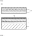
- FIG. 1 is a cross-sectional view showing a first display device 100 including a first window structure that can be attached and detached according to an embodiment of the present invention. However, it does not show a cross-sectional view of a strict meaning, and there may be components that may not appear in the cross-sectional view for convenience of explanation.
- the first display device 100 is configured by sequentially stacking a display 10, a bonding layer 12, a touch screen 14, an adhesion reduction layer 16, a detachable pattern 18, and a window 20.
- the detachable pattern 18 and the window 20 are referred to as a first window structure 22 together.
- the display 10 includes a liquid crystal display (LCD), an organic light emitting diode (OLED), an electrophoretic display (EPD) and the like, and quantum dots are also utilized.
- the bonding layer 12 firmly bonds the touch screen 14 to the display 10.
- a thermosetting adhesive or an ultraviolet curable adhesive may be used.
- the bonding layer 12 is not limited thereto, and an OCA tape or the like may also be used.
- the touch screen 14 has a conductive pattern formed on one side or both sides of an insulating layer made of metal oxide or plastic.
- the metal oxide is mainly applied to the conductive pattern, and the metal oxide includes ITO, ATO, ZnO, Cu, conductive polymer, silver nanowire or the like.
- the window 20 may use a transparent material without limit.
- the window 20 may include a glass substrate or a plastic substrate.
- the glass substrate may be tempered glass
- the plastic substrate may include any one or any one or more among polyethylene terephthalate (PET), polyethylene naphthalate (PEN), polyether sulfone (PES), polyimide (PI), polyarylate (PAR), polycarbonate (PC), polymethyl methacrylate (PMMA), and cycloolefin copolymer (COC).
- PET polyethylene terephthalate
- PEN polyethylene naphthalate
- PES polyether sulfone
- PI polyimide
- PAR polyarylate
- PC polycarbonate
- PMMA polymethyl methacrylate
- COC cycloolefin copolymer
- the window 20 may also be a stacked structure in which the tempered glass and the plastic substrate are formed as multiple layers.
- the window 20 may have a print layer transparent or implementing various functions.
- the print layer may apply any one or any one or more coatings among transparent, translucent and color coatings.
- the print layer may be formed by silk printing, inkjet printing using UV, inkjet printing using thermosetting, or transfer printing.
- a functional coating layer such as anti-fingerprint coating, antimicrobial coating, or anti-scratch coating may be formed on the window 20.
- the functional coating layer may be formed by wet coating of applying a coating liquid or dry coating such as deposition.
- the characteristics such as shielding, anti-reflection, blue light blocking, electromagnetic wave blocking, privacy and the like may be provided on the bottom of the glass substrate or the plastic substrate of the window 20.
- an opening for exposing a button, a camera, a speaker or the like may be formed in the window 20.
- an adhesion reduction layer 16 may be added on the touch screen 14 to facilitate attachment and detachment of the first window structure 22.
- the adhesion reduction layer 16 increases the slip property by lowering frictional force.
- the first window structure 22 may be easily attached to and detached from the touch screen 14 by the adhesion reduction layer 16.
- the adhesion reduction layer 16 may use a coating material of fluorine-based resin or silicon-based resin.
- the adhesion reduction layer 16 may be formed by depositing titania (TiO 2 ) or silica (SiO 2 ) on the touch screen 14 and then coating a fluorine-based resin or a silicon-based resin on the deposited touch screen 14.
- the fluorine-based resin or the silicon-based resin may be formed in an easy cleaning coating (ECC) method. If the adhesion reduction layer 16 is applied, generation of bubbles can be suppressed more effectively when the window 20 is attached. In addition, the adhesion reduction layer 16 allows a consumer to easily attach and detach the first window structure 22 by himself or herself without a tool.
- ECC easy cleaning coating
- the detachable pattern 18 When the adhesive force of the detachable pattern 18 is about 0.1gf/25mm to 500gf/25mm, the detachable pattern 18 has a self-adhesive force.
- the self-adhesive force is a property of the detachable pattern 18 adhering itself without bubbles by simply putting the detachable pattern 18 on the touch screen 14.
- the adhesion reduction layer 16 when the adhesion reduction layer 16 is applied to the touch screen 14, the self-adhesive force is improved more than when there is no adhesion reduction layer 16.
- the adhesive force according to an embodiment of the present invention may vary depending on the presence of the adhesion reduction layer 16.
- the adhesive force is 0.5gf/25mm to 500gf/25mm when the adhesion reduction layer 16 exists, whereas the adhesive force is 0.1gf/25mm to 200gf/25mm when the adhesion reduction layer 16 does not exist. If there exists an adhesion reduction layer 16 when a detachment pattern 18 of the same material and thickness is provided, it is easier to attach the first window structure 22 without bubbles. In addition, owing to the effect of the adhesion reduction layer 16, separation of the first window structure 22 occurs relatively easily.
- the adhesion reduction layer 16 of the present invention may have micro protrusions formed on all or part of it.
- the cross section of the micro projection may be angled, curved, or a combination thereof.
- the adhesion reduction layer 16 having micro protrusions formed thereon has an effect of preventing fingerprint, contamination and reflection by itself, and also has an effect of stably attaching and detaching the detachable pattern 18 without impairing clarity of the screen owing to the micro protrusions.
- the adhesion reduction layer 16 of the present invention may include a pattern formed of micro protrusions.
- the authenticity and engraved pattern of at least any one product among the window, the touch screen, and the display acquired through different channels can be confirmed.
- the micro protrusions and the pattern become translucent when they are separated from the detachable pattern 18, and when the detachable pattern 18 is attached to the adhesion reduction layer 16, the micro protrusions and the pattern disappear and the adhesion reduction layer 16 becomes transparent.
- FIG. 2 is plan views showing examples of a detachable pattern 18 applied to a first window structure 22 that can be attached and detached according to an embodiment of the present invention. It merely shows some examples of the detachable pattern 18 herein, and various modifications can be made within the scope of the present invention.
- e is an adhesive layer having an adhesive force of about 0.1gf/25mm to 500gf/25mm
- f is a cured layer formed by curing e and having an adhesive force lower than that of e. That is, e may be referred to as an adhesive layer that can be cured, and f may be referred to as a cured layer. At this point, the area occupied by the cured layer (f) may be 5 to 95% of the adhesive layer (e) and the cured layer (f).
- the curable adhesive layer (e) may be a thermosetting adhesive layer or an ultraviolet curable adhesive layer.
- the thermosetting adhesive layer may be diversely selected within the scope of the present invention. For example, there are an acrylic resin containing a hydroxyl group, an acrylic resin containing a hydroxyl group and having a weight average molecular weight of 100,000 to 1,000,000, a resin composition containing block isocyanate as a main component, a composition containing a hydroxyl group containing acrylic resin and block isocyanate as essential components, a composition containing a compound having two or more functional groups capable of reacting to an isocyanate group in one molecule and a block isocyanate, and the like.
- the ultraviolet curable adhesive layer is made by, for example, mixing various acrylic monomers and an ultraviolet curing catalyst with a polyurethane resin, an epoxy resin, or a polyester resin.
- a urethane or acrylate oligomer, a reactive monomer, a photoinitiator and a leveling agent are mixed as the ultraviolet reactive coating material.
- the urethane acrylate oligomer contains an aliphatic, cyclic aliphatic or aromatic compound or an oligomer of these compounds, and have a chemical formula in which polyester polyols or polyether polyols are contained in the molecular structure.
- the photoinitiator uses a general polymerization initiator activated by ultraviolet rays, and particularly, hydroxycyclohexyl phenyl ketone, benzophenol, and phenyl-2-hydroxy-2-phenyl ketone are mainly used.
- curable adhesive layers (e) and cured layers (f) are disposed in the shape of a stripe.
- the order of disposing the adhesive layers (e) and the cured layers (f) may vary depending on the shape of the first window structure 22 to which the first detachable pattern 18a of the present invention is applied.
- the cured layers (f) may be mainly disposed in the bezel region.
- the width of the adhesive layers (e) and the cured layers (f) configuring the first detachable pattern 18a may be appropriately adjusted, respectively.
- the shape of the strip in the drawing is a rectangular shape having a predetermined thickness, in some cases, the shape may be modified to a wave shape or the like.
- a second detachable pattern 18b(b) is formed in the shape of a lattice, and an adhesive layer (e) or a cured layer (f) is disposed in each cell.
- the order of disposing the adhesive layers (e) and the cured layers (f) may vary depending on the shape of the first window structure 22 to which the second detachable pattern 18b of the present invention is applied.
- the cured layers (f) may be mainly disposed in the bezel region.
- the areas of the adhesive layers (e) and the cured layers (f) configuring the second detachable pattern 18a may be appropriately adjusted.
- the shape of the strip ( ⁇ cells) in the drawing is a rectangular shape having a predetermined thickness ( ⁇ area), in some cases, it may include a shape such as a circle, an ellipse, a wave or the like.
- a third detachable pattern 18c(c) adhesive layers (e) and a cured layer (f) closed in the shape of a fence are disposed.
- the order of disposing the adhesive layers (e) and the cured layer (f) may vary depending on the shape of the first window structure 22 to which the third detachable pattern 18c of the present invention is applied.
- the cured layer (f) may be mainly disposed in the bezel region.
- the areas of the adhesive layers (e) and the cured layer (f) configuring the third detachable pattern 18c may be appropriately adjusted.
- the shape of a fence in the drawing may be a rectangular shape having a predetermined thickness, in some cases, the shape may be modified to a wave shape or the like.
- a fourth detachable pattern 18d(d) one among the adhesive layer (e) and the cured layer (f) passes through some of the closed fence of the third detachable pattern 18c.
- the order of disposing the adhesive layers (e) and the cured layer (f) may vary depending on the shape of the first window structure 22 to which the fourth detachable pattern 18d of the present invention is applied.
- the cured layer (f) may be mainly disposed in the bezel region.
- the areas of the adhesive layers (e) and the cured layer (f) configuring the fourth detachable pattern 18d may be appropriately adjusted.
- the shape of the fence in the drawing may be a rectangular shape having a predetermined thickness, in some cases, the shape may be modified to a wave shape or the like.
- the detachable pattern 18 allows to freely adjust adhesive force of attaching and detaching a window.
- the adhesive force of the detachable pattern 18 is changed.
- the adhesive layers (e) and the cured layers (f) of the detachable pattern 18 are different from each other in the adhesive force, the possibility of removing bubbles increases.
- the first window structure 22 of the present invention is separately manufactured and protected by a release film.
- the release film is removed to attach the first window structure 22 to the adhesion reduction layer 16.
- the detachable pattern 18 is exposed.
- the first window structure 22 having the exposed detachable pattern 18 is manually attached to the touch screen 14 or the adhesion reduction layer 16, a display mounted with the window 20 may be completed.
- the first window structure 22 is manually separated, and a new first window structure 22 may be attached.
- FIG. 3 is a cross-sectional view showing a second display device 200 including a first window structure 22 that can be attached and detached according to an embodiment of the present invention. However, it does not show a cross-sectional view of a strict meaning, and there may be components that may not appear in the cross-sectional view for convenience of explanation.
- the second display device 200 is the same as the first display device 100 except that the bonding layer 12 does not exist.
- the matters overlapped with the above description will be omitted or briefly described.
- a display 10, a touch screen 14, an adhesion reduction layer 16, and a first window structure 22 configure sequential layers.
- the first window structure 22 includes a detachable pattern 18.
- the detachable pattern 18 is divided into an adhesive layer (e) that can be cured and a cured layer (f) formed by curing the adhesive layer, and the area occupied by the cured layer (f) may be 5 to 95% of the adhesive layer (e) and the cured layer (f). Adhesive force of the detachable pattern 18 may be adjusted and removal of bubbles may be facilitated by varying the area.
- the touch screen 14 is manufactured by forming a conductive pattern directly on the display 10. That is, the touch screen 14 is formed together with the conductive pattern formed on the display 10.
- the first window structure 22 includes the detachable pattern 18 described above.
- the second display device 200 may be provided with an adhesion reduction layer 16, like the first display device 100.
- the materials, functions and the like of the adhesion reduction layer 16 are the same as those described in the first display device 100.
- the adhesive force according to an embodiment of the present invention may vary depending on the presence of the adhesion reduction layer 16.
- the adhesive force is 0.5gf/25mm to 500gf/25mm when the adhesion reduction layer 16 exists, whereas the adhesive force is 0.1gf/25mm to 200gf/25mm when the adhesion reduction layer 16 does not exist. If there exists an adhesion reduction layer 16 when a detachment pattern 18 of the same material and thickness is provided, it is easy to attach the first window structure 22 without bubbles. In addition, owing to the effect of the adhesion reduction layer 16 ( ⁇ 22), separation of the first window structure 22 occurs relatively easily.
- an additional component for providing various functions may be further provided between the window 20 and the detachable pattern 18 of the first window structure 22 according to an embodiment of the present invention.
- the additional component may include an optically clear adhesive (OCA) layer, a shatterproof layer, and the like, and if necessary, a print layer and a functional coating layer may be appropriately formed.
- OCA optically clear adhesive
- the detachable pattern 18 may be formed on the transparent synthetic resin film. Since such an additional component is already well known, detailed description thereof will be omitted.
- FIG. 4 is a cross-sectional view showing a third display device 300 including a second window structure 26 that can be attached and detached according to an embodiment of the present invention. However, it does not show a cross-sectional view of a strict meaning, and there may be components that may not appear in the cross-sectional view for convenience of explanation.
- the third display device 300 is the same as the first display device 100 except that a touch screen cover layer 24 is adopted. Accordingly, the detailed description of the same reference numerals will be omitted.
- the second window structure 26 may further include additional components, as is described in the first window structure 22.
- the third display device 300 may be implemented by sequentially stacking a display 10, a bonding layer 12, a touch screen 14, a cover layer 24, an adhesion reduction layer 16, a detachable pattern 18, and a window 20.
- the display 10 may be directly bonded to the touch screen 14 without the bonding layer 12, like the second display device 200.
- the second window structure 26 includes the detachable pattern 18.
- the detachable pattern 18 is divided into an adhesive layer (e) that can be cured and a cured layer (f) formed by curing the adhesive layer, and the area occupied by the cured layer (f) may be 5 to 95% of the adhesive layer (e) and the cured layer (f). Adhesive force of the detachable pattern 18 may be adjusted and removal of bubbles may be facilitated by varying the area.
- a conductive pattern for forming the touch screen 14 is disposed on the top or bottom of the cover layer 24.
- the cover layer 24 may be regarded as a part of the touch screen 14.
- the cover layer 24 prevents the touch screen 14 from being damaged by impact or contamination.
- the third display device 300 configures the touch screen 14 by forming a conductive pattern directly on the display 10. In this case, the touch screen cover layer 24 may be positioned on the top of the display 10.
- the cover layer 24 When the cover layer 24 is covered with the second window structure 26, it is positioned inside the third display device 300. Since the cover layer 24 is positioned inside, there is no worry that the cover layer 24 is exposed to the outside of the third display device 300 and damaged by impact or the like.
- the cover layer 24 may include a print layer or a functional coating layer, and may beautify the third display device 300 through various designs or translucence. In addition, the cover layer 24 may exclude the effect of windings and steps generated by various patterns, circuits or the like of the touch screen 14. When the effect of windings and steps disappears, attachment and detachment by the detachment pattern 18 becomes easier.
- the cover layer 24 may use a transparent material without limit.
- the window 20 may include a glass substrate or a plastic substrate.
- the glass substrate may be tempered glass or untempered glass, and in addition, the plastic substrate may include any one or more among polyethylene terephthalate (PET), polyethylene naphthalate (PEN), polyether sulfone (PES), polyimide (PI), polyarylate (PAR), polycarbonate (PC), polymethyl methacrylate (PMMA), and cycloolefin copolymer (COC).
- PET polyethylene terephthalate
- PEN polyethylene naphthalate
- PES polyether sulfone
- PI polyimide
- PAR polyarylate
- PC polycarbonate
- PMMA polymethyl methacrylate
- COC cycloolefin copolymer
- the thickness of the cover layer 24 is sufficient if the touch screen 14 is not damaged in the process of using the third display device 300.
- the third display device 300 may be provided with an adhesion reduction layer 16, like the first display device 100.
- the materials, functions and the like of the adhesion reduction layer 16 are the same as those described in the first display device 100.
- the adhesive force according to an embodiment of the present invention may vary depending on the presence of the adhesion reduction layer 16.
- the adhesive force is 0.5gf/25mm to 500gf/25mm when the adhesion reduction layer 16 exists, whereas the adhesive force is 0.1gf/25mm to 200gf/25mm when the adhesion reduction layer 16 does not exist. If there exists an adhesion reduction layer 16 when a detachment pattern 18 of the same material and thickness is provided, it is easy to attach the second window structure 26 without bubbles. In addition, owing to the effect of the adhesion reduction layer 16, separation of the second window structure 26 occurs relatively easily.
- the detachable pattern 18 When the adhesive force of the detachable pattern 18 is about 0.1gf/25mm to 500gf/25mm, the detachable pattern 18 has a self-adhesive force.
- the self-adhesive force is a property of the detachable pattern 18 adhering itself without bubbles by simply putting the detachable pattern 18 on the cover layer 24.
- the adhesion reduction layer 16 when the adhesion reduction layer 16 is applied to the cover layer 24, the self-adhesive force is improved more than when there is no adhesion reduction layer 16.
- the window structure may be replaced by selecting and attaching a new window structure. Specifically, the broken window structure is removed and replaced by attaching a new window structure. A customer himself or herself may manually perform the process of replacing the window structure, and the time required for replacing the window structure is very short. In addition, since only the window structure needs to be removed, recycle of the display device is easy. Furthermore, since the window structure is attached and detached, it can be easily attached without bubbles. Since a manufacturer only needs to manufacture only the parts other than the window structure and does not need to perform an adhering process, the manufacturing process is simplified.
- FIG. 5 is a cross-sectional view showing a fourth display 400 device including a third window structure 30 that can be attached and detached according to an embodiment of the present invention. However, it does not show a cross-sectional view of a strict meaning, and there may be components that may not appear in the cross-sectional view for convenience of explanation.
- the fourth display device 400 is basically the same as the first display device 100 except that the position of each layer is changed.
- the matters overlapped with the above description will be omitted or briefly described.
- the fourth display device 400 is configured by sequentially stacking a display 10, an adhesion reduction layer 16, a detachable pattern 18, a touch screen 14, a bonding layer 12, and a window 20.
- the window 20, the bonding layer 12, the touch screen 14, and the detachable pattern 18 configure the third window structure 30.
- the third window structure 30 includes the detachable pattern 18.
- the detachable pattern 18 is divided into an adhesive layer (e) that can be cured and a cured layer (f) formed by curing the adhesive layer, and the area occupied by the cured layer (f) may be 5 to 95% of the adhesive layer (e) and the cured layer (f). Adhesive force of the detachable pattern 18 may be adjusted and removal of bubbles may be facilitated by varying the area.
- the display 10 includes a liquid crystal display (LCD), an organic light emitting diode (OLED), an electrophoretic display (EPD) and the like, and quantum dots are also utilized.
- a thermosetting adhesive or an ultraviolet curable adhesive may be used for the bonding layer 12.
- the bonding layer 12 is not limited thereto, and an OCA tape or the like may also be used.
- the touch screen 14 has conductive patterns formed on one side or both sides of an insulating layer made of metal oxide or plastic. Metal oxide is mainly applied to the conductive pattern, and the metal oxide includes ITO, ATO, ZnO, Cu, conductive polymer, silver nanowire or the like.
- an adhesion reduction layer 16 may be added on the display 10 to facilitate attachment and detachment of the third window structure 30.
- the adhesion reduction layer 16 increases the slip property by increasing the contact angle.
- the third window structure 30 may be easily attached to and detached from the touch screen 14 by the adhesion reduction layer 16.
- the adhesion reduction layer 16 may use a coating material of fluorine-based resin or silicon-based resin.
- the adhesion reduction layer 16 may be formed by depositing titania (TiO 2 ) or silica (SiO 2 ) on the display 10, and then coating a fluorine-based resin or a silicon-based resin on the deposited display 10. At this point, the fluorine-based resin or the silicon-based resin may be formed by easy cleaning coating (ECC) method.
- ECC easy cleaning coating
- adhesion reduction layer 16 If the adhesion reduction layer 16 is applied, generation of bubbles can be suppressed more effectively when the touch screen 14 is attached.
- the adhesion reduction layer 16 ( ⁇ 60) allows a consumer to easily attach and detach the third window structure 30 by himself or herself without a tool.
- the detachable pattern 18 When the adhesive force of the detachable pattern 18 is about 0.1gf/25mm to 500gf/25mm, the detachable pattern 18 has a self-adhesive force.
- the self-adhesive force is a property of the detachable pattern 18 adhering itself without bubbles by simply putting the detachable pattern 18 on the touch screen 14.
- the adhesion reduction layer 16 when the adhesion reduction layer 16 is applied to the display 10, the self-adhesive force is improved more than when there is no adhesion reduction layer 16.
- the adhesive force according to an embodiment of the present invention may vary depending on the presence of the adhesion reduction layer 16.
- the adhesive force is 0.5gf/25mm to 500gf/25mm when the adhesion reduction layer 16 exists. If the adhesion reduction layer 16 does not exist, the adhesive force is 0.1gf/25mm to 200gf/25mm. If there exists an adhesion reduction layer 16 when a detachment pattern 18 of the same material and thickness is provided, it is easy to attach the third window structure 30 without bubbles. In addition, owing to the effect of the adhesion reduction layer 16, separation of the third window structure 30 occurs relatively easily.
- the third window structure 30 of the present invention is separately manufactured and protected by a release film.
- the release film is removed to attach the third window structure 30 to the display 10.
- the detachable pattern 18 is exposed.
- the third window structure 30 having the exposed detachable pattern 18 is manually attached to the display 10, a display mounted with the window 20 may be completed. Accordingly, unlike the prior art, a precise bonding process is not required.
- the third window structure 30 is damaged or to be replaced, the third window structure 30 is manually separated, and a new third window structure 30 may be attached.
- FIG. 6 is a cross-sectional view showing a fifth display device 500 including a fourth window structure 34 that can be attached and detached according to an embodiment of the present invention. However, it does not show a cross-sectional view of a strict meaning, and there may be components that may not appear in the cross-sectional view for convenience of explanation.
- the fifth display device 500 is the same as the first display device 100 except that the bonding layer 12 is replaced with a detachable layer 32.
- the matters overlapped with the above description will be omitted or briefly described.
- a display 10, an adhesion reduction layer 16, a detachable pattern 18, a touch screen 14, a detachable layer 32, and a window 20 are sequentially stacked in the fifth display device 500.
- the window 20, the detachable layer 32, the touch screen 14, and the detachable pattern 18 configure the fourth window structure 34.
- the fourth window structure 34 includes the detachable pattern 18.
- the detachable pattern 18 is divided into an adhesive layer (e) that can be cured and a cured layer (f) formed by curing the adhesive layer, and the area occupied by the cured layer (f) may be 5 to 95% of the adhesive layer (e) and the cured layer (f). Adhesive force of the detachable pattern 18 may be adjusted and removal of bubbles may be facilitated by varying the area.
- the fourth window structure 34 is attached to and detached from the display 10 by the detachable pattern 18.
- the detachable pattern 18 may be attached to the display 10 while the release film is removed.
- the fourth window structure 34 may be attached to and detached from the touch screen 14 by the detachable layer 32.
- the fourth window structure 34 includes the detachable pattern 18 and the detachable layer 32 that can be attached to and detached from the display 10 and the touch screen 20 ( ⁇ 14), respectively.
- any transparent material may be used as the detachable layer 32, it may be an acrylic polymer, a silicon polymer, a urethane polymer, an adhesive made by mixing a crosslinking agent with an ultraviolet curable resin, a mixture thereof, or a copolymer thereof.
- the detachable layer 32 may be a single layer or a multilayer made of different materials in each layer, and at least one may be a single layer. In the multilayer, a material which forms each layer may be appropriately selected according to the environment in which the detachable layer 32 of the present invention is used. Thickness of the detachable layer 32 is acceptable if the adhesion is sufficient, and thickness of 10 to 200 micrometers is preferable. It is apparent that the thickness can be obtained through repeated experiments by those skilled in the art.
- an additional component for providing various functions may be further provided between the window 20 and the detachable layer 32 or between the touch screen 14 and the detachable pattern 18 of the third and fourth window structures 30 and 34 according to an embodiment of the present invention.
- the additional component may include an optically clear adhesive (OCA) layer, a shatterproof layer, and the like, and if necessary, a print layer and a functional coating layer may be appropriately formed.
- OCA optically clear adhesive
- the detachable pattern 18 may be formed on the transparent synthetic resin film. Since such an additional component is already well known, detailed description thereof will be omitted.
- FIG. 7 is a cross-sectional view showing a sixth display device 600 including a fifth window structure 36 that can be attached and detached according to an embodiment of the present invention. However, it does not show a cross-sectional view of a strict meaning, and there may be components that may not appear in the cross-sectional view for convenience of explanation.
- the sixth display device 600 is the same as the fourth display device 400 except that the bonding layer 12 is not provided. Accordingly, the detailed description of the same reference numerals will be omitted.
- the fifth window structure 36 may further include additional components, as is described in the third window structure 30.
- the sixth display device 600 is configured by stacking a display 10, an adhesion reduction layer 16, a detachable pattern 18, a touch screen 14, and a window 20.
- the window 20, the touch screen 14, and the detachable layer ( ⁇ pattern) 18 configure the fifth window structure 36.
- the fifth window structure 36 includes the detachable pattern 18.
- the detachable pattern 18 is divided into an adhesive layer (e) that can be cured and a cured layer (f) formed by curing the adhesive layer, and the area occupied by the cured layer (f) may be 5 to 95% of the adhesive layer (e) and the cured layer (f).
- Adhesive force of the detachable pattern 18 may be adjusted and removal of bubbles may be facilitated by varying the area.
- the touch screen 14 is manufactured by forming a conductive pattern directly under the window 20. That is, the touch screen 14 is formed together with the conductive pattern formed under the window 20.
- the sixth display device 600 may be provided with an adhesion reduction layer 16, like the fourth display device 400.
- the materials, functions and the like of the adhesion reduction layer 16 are the same as those described in the fourth display device 400.
- the adhesive force according to an embodiment of the present invention may vary depending on the presence of the adhesion reduction layer 16.
- the adhesive force is 0.5gf/25mm to 500gf/25mm when the adhesion reduction layer 16 exists, whereas the adhesive force is 0.1gf/25mm to 200gf/25mm when the adhesion reduction layer 16 does not exist. If there exists an adhesion reduction layer 16 when a detachment pattern 18 of the same material and thickness is provided, it is easy to attach the fifth window structure 36 without bubbles. In addition, owing to the effect of the adhesion reduction layer 16, separation of the fifth window structure 36 occurs relatively easily.
- the detachable pattern 18 When the adhesive force of the detachable pattern 18 is about 0.1gf/25mm to 500gf/25mm, the detachable pattern 18 has a self-adhesive force.
- the self-adhesive force is a property of the detachable pattern 18 adhering itself without bubbles by simply putting the detachable pattern 18 on the display 10.
- the adhesion reduction layer 16 when the adhesion reduction layer 16 is applied to the display 10, the self-adhesive force is improved more than when there is no adhesion reduction layer 16.
- connection units may be made to face each other in predetermined areas of the display 10 and the touch screen 14, respectively.
- part of the detachable pattern 18 of the touch screen 14 ⁇ the touch screen 14 and the detachable pattern 18
- the connection units are connected to each other. In this manner, connections of the first to sixth display devices 100, 200, 300, 400, 500 and 600 may be implemented.
- the window structure may be replaced by selecting and attaching a new window structure. Specifically, the broken window structure is removed and replaced by attaching a new window structure. A customer himself or herself may perform the process of replacing the window structure, and the time required for replacing the window structure is very short. In addition, since only the window structure needs to be removed, recycle of the display device is easy. Furthermore, since the window structure is attached and detached by adhesion, it can be easily attached without bubbles. Since a manufacturer only needs to manufacture only the parts other than the window structure and does not need to perform an adhering process, the manufacturing process is simplified. Particularly, when an adhesion reduction layer exists, it is easier to attach the window structure without bubbles, and owing to the effect of the adhesion reduction layer, separation of the window structure occurs relatively easily.
- the appearance of the display device of the present invention can be diversely designed.
- the display device of the present invention may be designed to have a beautiful shape, various colors and patterns, and the like. This is since that when an original window structure is separated and a new structure is attached, the appearance of the window structure can be changed in a desired design. Conventionally, it needs to remove adhesion of the window structure and reattach a new window structure to change the design.
- the design is changed by detaching an existing window structure and attaching a new window structure. Accordingly, unlike a conventional window structure, the window structure of the present invention is not an essential component fixed to a display device and may be treated as a disposable component that can be attached and detached as needed. If the design is diversified in this way, the manufacturer of the display device does not need to provide a service corresponding to the design later.
- the display device having a detachable pattern of the present invention since a window formed with a detachable pattern having an adhesive force of 0.1gf/25mm to 500gf/25mm is attached and detached, a damaged window is easily replaced, and separation of the window is simple. If the areas of the adhesive layer (e) and the cured layer (f) of the detachable pattern are changed, the adhesive force of the detachable pattern 18 can be adjusted, and removal of bubbles is facilitated. In addition, since the detachable pattern of the present invention has a self-adhesive force, it can be easily attached and detached without bubbles.
- the display device of the present invention may satisfy desires of consumers. Furthermore, since anyone may easily replace a window by attaching and detaching, it can be treated as a disposable component rather than an essential component fixed to the display device.
- a separate means such as a groove or the like may be provided in the injection mold of the display device so that the window structure may be attached and detached more easily.
Landscapes
- Engineering & Computer Science (AREA)
- General Engineering & Computer Science (AREA)
- Theoretical Computer Science (AREA)
- Human Computer Interaction (AREA)
- Physics & Mathematics (AREA)
- General Physics & Mathematics (AREA)
- Devices For Indicating Variable Information By Combining Individual Elements (AREA)
- Liquid Crystal (AREA)
- Position Input By Displaying (AREA)
Applications Claiming Priority (3)
| Application Number | Priority Date | Filing Date | Title |
|---|---|---|---|
| KR20160127307 | 2016-10-03 | ||
| KR1020170123028A KR102146150B1 (ko) | 2016-10-03 | 2017-09-23 | 탈부착 패턴을 가진 디스플레이 장치 |
| PCT/KR2018/009859 WO2019059546A1 (fr) | 2016-10-03 | 2018-08-27 | Dispositif d'affichage comportant un motif attachable/détachable |
Publications (3)
| Publication Number | Publication Date |
|---|---|
| EP3686716A1 true EP3686716A1 (fr) | 2020-07-29 |
| EP3686716A4 EP3686716A4 (fr) | 2020-11-04 |
| EP3686716B1 EP3686716B1 (fr) | 2023-07-19 |
Family
ID=61975938
Family Applications (1)
| Application Number | Title | Priority Date | Filing Date |
|---|---|---|---|
| EP18859062.4A Active EP3686716B1 (fr) | 2016-10-03 | 2018-08-27 | Dispositif d'affichage comportant un motif attachable/détachable |
Country Status (6)
| Country | Link |
|---|---|
| US (1) | US11073924B2 (fr) |
| EP (1) | EP3686716B1 (fr) |
| JP (1) | JP2020534577A (fr) |
| KR (1) | KR102146150B1 (fr) |
| CN (1) | CN111095177A (fr) |
| WO (1) | WO2019059546A1 (fr) |
Families Citing this family (8)
| Publication number | Priority date | Publication date | Assignee | Title |
|---|---|---|---|---|
| KR102241293B1 (ko) * | 2018-05-14 | 2021-04-16 | 김영수 | 점착조절층을 이용한 표시장치 |
| WO2019221460A1 (fr) * | 2018-05-14 | 2019-11-21 | Kim Young Su | Dispositif d'affichage utilisant une couche de régulation d'adhérence |
| WO2020040489A1 (fr) * | 2018-08-20 | 2020-02-27 | 김영수 | Dispositif d'indication de fixation/séparation |
| KR102241276B1 (ko) * | 2018-08-20 | 2021-04-16 | 김영수 | 일체형 커버를 포함하는 탈부착 표시장치 |
| WO2021125764A1 (fr) * | 2019-12-20 | 2021-06-24 | 김영수 | Dispositif d'affichage pouvant être fixé/détaché comprenant une couche d'habillage composite |
| KR102437333B1 (ko) * | 2019-12-20 | 2022-08-29 | 김영수 | 복합커버층을 포함하는 탈부착 표시장치 |
| KR102776785B1 (ko) * | 2020-04-22 | 2025-03-11 | 삼성디스플레이 주식회사 | 표시 장치 및 표시 장치의 제조 방법 |
| KR102395757B1 (ko) * | 2021-01-28 | 2022-05-10 | (주)유티아이 | 플렉시블 커버 윈도우 |
Family Cites Families (17)
| Publication number | Priority date | Publication date | Assignee | Title |
|---|---|---|---|---|
| CA2406693C (fr) * | 2000-04-24 | 2011-02-15 | Avery Dennison Corporation | Articles adhesifs a chasse d'air amelioree et procedes de fabrication correspondants |
| JP2008027747A (ja) * | 2006-07-21 | 2008-02-07 | Fujitsu Ltd | 電池充電用燃料電池 |
| JP5269343B2 (ja) * | 2007-04-27 | 2013-08-21 | 株式会社半導体エネルギー研究所 | 半導体装置の作製方法 |
| US20100066683A1 (en) * | 2008-09-17 | 2010-03-18 | Shih-Chang Chang | Method for Transferring Thin Film to Substrate |
| KR101393778B1 (ko) * | 2010-11-22 | 2014-05-13 | (주)엘지하우시스 | 양면 점착 시트 및 이를 포함하는 터치 패널 표시장치 |
| KR101321341B1 (ko) | 2011-07-01 | 2013-10-23 | 정형근 | 터치스크린 패널 보호용 필터 |
| JP2013125262A (ja) * | 2011-12-16 | 2013-06-24 | Technology Research Association For Advanced Display Materials | 貼合材料、表示素子及び表示素子の製造方法 |
| KR20140123735A (ko) * | 2013-04-15 | 2014-10-23 | 삼성디스플레이 주식회사 | 점착캡슐을 갖는 점착제 및 상기 점착제에 의하여 형성된 점착층을 갖는 유기발광 표시장치 |
| KR20150034829A (ko) * | 2013-08-30 | 2015-04-06 | 주식회사 엔씰텍 | 플렉시블 정보 표시 소자 제조용 지지 기판, 이의 제조 방법, 이를 이용하여 제조된 플렉시블 정보 표시 소자 및 이의 제조방법 |
| CN105446508B (zh) * | 2014-06-19 | 2018-12-25 | 宸鸿科技(厦门)有限公司 | 触控显示装置 |
| KR102246292B1 (ko) * | 2014-07-29 | 2021-04-30 | 삼성디스플레이 주식회사 | 휴대용 전자장치 |
| KR101562874B1 (ko) * | 2014-12-03 | 2015-10-26 | 엘지디스플레이 주식회사 | 보호 필름 및 그를 포함한 디스플레이 모듈과 그 제조 방법 |
| KR101574923B1 (ko) * | 2015-01-20 | 2015-12-04 | 김영수 | 탈부착이 가능한 윈도우를 포함하는 디스플레이 장치 및 그 탈부착 방법 |
| JP6460525B2 (ja) * | 2015-01-30 | 2019-01-30 | 藤森工業株式会社 | 接着性樹脂層、接着性樹脂フィルム、積層体及び積層体の製造方法 |
| KR102342869B1 (ko) * | 2015-02-26 | 2021-12-23 | 삼성디스플레이 주식회사 | 가요성 표시 장치 및 이의 제조방법 |
| KR101675225B1 (ko) * | 2015-04-08 | 2016-11-10 | 김영수 | 탈부착층을 가진 디스플레이 장치 및 그 제조방법 |
| KR101959632B1 (ko) * | 2016-10-03 | 2019-03-18 | 김영수 | 탈부착 조절을 위한 미세돌기를 포함하는 디스플레이 장치 및 그 제조방법 |
-
2017
- 2017-09-23 KR KR1020170123028A patent/KR102146150B1/ko not_active Expired - Fee Related
-
2018
- 2018-08-27 WO PCT/KR2018/009859 patent/WO2019059546A1/fr not_active Ceased
- 2018-08-27 CN CN201880060637.6A patent/CN111095177A/zh active Pending
- 2018-08-27 JP JP2020516383A patent/JP2020534577A/ja active Pending
- 2018-08-27 US US16/649,358 patent/US11073924B2/en not_active Expired - Fee Related
- 2018-08-27 EP EP18859062.4A patent/EP3686716B1/fr active Active
Also Published As
| Publication number | Publication date |
|---|---|
| KR20180037108A (ko) | 2018-04-11 |
| EP3686716B1 (fr) | 2023-07-19 |
| EP3686716A4 (fr) | 2020-11-04 |
| US20200225781A1 (en) | 2020-07-16 |
| CN111095177A (zh) | 2020-05-01 |
| JP2020534577A (ja) | 2020-11-26 |
| WO2019059546A1 (fr) | 2019-03-28 |
| US11073924B2 (en) | 2021-07-27 |
| KR102146150B1 (ko) | 2020-08-19 |
Similar Documents
| Publication | Publication Date | Title |
|---|---|---|
| US11073924B2 (en) | Apparatus of display having detachable pattern | |
| JP6330919B2 (ja) | 着脱可能なウィンドウを含むディスプレイ装置、及びその着脱方法 | |
| US10696011B2 (en) | Display device including fine bump for adjusting attachment and detachment and manufacturing method therefor | |
| KR101675225B1 (ko) | 탈부착층을 가진 디스플레이 장치 및 그 제조방법 | |
| US11301070B2 (en) | Apparatus of display having adhesion reduction layer formed micro protrusion design | |
| KR102241293B1 (ko) | 점착조절층을 이용한 표시장치 | |
| KR20180037088A (ko) | 탈부착층을 포함하는 디스플레이 장치 및 그 제조방법 | |
| KR102146151B1 (ko) | 표면개질 탈부착 시트를 포함하는 디스플레이 장치 | |
| KR101911698B1 (ko) | 탈부착 유동층을 가진 디스플레이 장치 | |
| US11324133B2 (en) | Attachable/detachable display device comprising polarizing film | |
| KR20180026830A (ko) | 탈부착층을 가진 디스플레이 장치 | |
| KR102144652B1 (ko) | 탈부착 패턴을 가진 디스플레이 장치 | |
| EP3293568A1 (fr) | Dispositif d'affichage ayant une couche amovible et son procédé de fabrication | |
| KR20180037103A (ko) | 탈부착 시트를 포함하는 디스플레이 장치 | |
| JP6330871B2 (ja) | 着脱層を有するディスプレイ装置、及びその製造方法{Apparatus of display having detachable layer and method of manufacturing the display} | |
| KR20210016017A (ko) | 표면개질된 탈부착층을 이용한 표시장치 | |
| KR20210016018A (ko) | 표면개질된 탈부착층을 이용한 표시장치 | |
| WO2018066853A1 (fr) | Dispositif d'affichage comprenant une bosse fine pour ajuster la fixation et le détachement et son procédé de fabrication | |
| WO2018066854A1 (fr) | Dispositif d'affichage comprenant une feuille détachable |
Legal Events
| Date | Code | Title | Description |
|---|---|---|---|
| STAA | Information on the status of an ep patent application or granted ep patent |
Free format text: STATUS: THE INTERNATIONAL PUBLICATION HAS BEEN MADE |
|
| PUAI | Public reference made under article 153(3) epc to a published international application that has entered the european phase |
Free format text: ORIGINAL CODE: 0009012 |
|
| STAA | Information on the status of an ep patent application or granted ep patent |
Free format text: STATUS: REQUEST FOR EXAMINATION WAS MADE |
|
| 17P | Request for examination filed |
Effective date: 20200422 |
|
| AK | Designated contracting states |
Kind code of ref document: A1 Designated state(s): AL AT BE BG CH CY CZ DE DK EE ES FI FR GB GR HR HU IE IS IT LI LT LU LV MC MK MT NL NO PL PT RO RS SE SI SK SM TR |
|
| AX | Request for extension of the european patent |
Extension state: BA ME |
|
| A4 | Supplementary search report drawn up and despatched |
Effective date: 20201005 |
|
| RIC1 | Information provided on ipc code assigned before grant |
Ipc: G06F 3/041 20060101AFI20200929BHEP Ipc: B32B 7/06 20190101ALI20200929BHEP |
|
| DAV | Request for validation of the european patent (deleted) | ||
| DAX | Request for extension of the european patent (deleted) | ||
| STAA | Information on the status of an ep patent application or granted ep patent |
Free format text: STATUS: EXAMINATION IS IN PROGRESS |
|
| 17Q | First examination report despatched |
Effective date: 20210806 |
|
| GRAP | Despatch of communication of intention to grant a patent |
Free format text: ORIGINAL CODE: EPIDOSNIGR1 |
|
| STAA | Information on the status of an ep patent application or granted ep patent |
Free format text: STATUS: GRANT OF PATENT IS INTENDED |
|
| RIC1 | Information provided on ipc code assigned before grant |
Ipc: G06F 3/041 20060101ALI20221223BHEP Ipc: B32B 27/36 20060101ALI20221223BHEP Ipc: B32B 27/32 20060101ALI20221223BHEP Ipc: B32B 27/28 20060101ALI20221223BHEP Ipc: B32B 17/06 20060101ALI20221223BHEP Ipc: B32B 27/12 20060101AFI20221223BHEP |
|
| RIC1 | Information provided on ipc code assigned before grant |
Ipc: B32B 27/30 19680901ALI20230111BHEP Ipc: B32B 27/08 19680901ALI20230111BHEP Ipc: B32B 17/06 19680901ALI20230111BHEP Ipc: B32B 27/36 19680901ALI20230111BHEP Ipc: B32B 27/32 19680901ALI20230111BHEP Ipc: B32B 27/28 19680901ALI20230111BHEP Ipc: B32B 7/12 19680901ALI20230111BHEP Ipc: B32B 7/06 19680901ALI20230111BHEP Ipc: G06F 3/041 20060101AFI20230111BHEP |
|
| INTG | Intention to grant announced |
Effective date: 20230131 |
|
| GRAS | Grant fee paid |
Free format text: ORIGINAL CODE: EPIDOSNIGR3 |
|
| GRAA | (expected) grant |
Free format text: ORIGINAL CODE: 0009210 |
|
| STAA | Information on the status of an ep patent application or granted ep patent |
Free format text: STATUS: THE PATENT HAS BEEN GRANTED |
|
| AK | Designated contracting states |
Kind code of ref document: B1 Designated state(s): AL AT BE BG CH CY CZ DE DK EE ES FI FR GB GR HR HU IE IS IT LI LT LU LV MC MK MT NL NO PL PT RO RS SE SI SK SM TR |
|
| REG | Reference to a national code |
Ref country code: GB Ref legal event code: FG4D |
|
| REG | Reference to a national code |
Ref country code: CH Ref legal event code: EP |
|
| REG | Reference to a national code |
Ref country code: DE Ref legal event code: R096 Ref document number: 602018053787 Country of ref document: DE |
|
| REG | Reference to a national code |
Ref country code: IE Ref legal event code: FG4D |
|
| REG | Reference to a national code |
Ref country code: LT Ref legal event code: MG9D |
|
| REG | Reference to a national code |
Ref country code: NL Ref legal event code: MP Effective date: 20230719 |
|
| REG | Reference to a national code |
Ref country code: AT Ref legal event code: MK05 Ref document number: 1590126 Country of ref document: AT Kind code of ref document: T Effective date: 20230719 |
|
| PG25 | Lapsed in a contracting state [announced via postgrant information from national office to epo] |
Ref country code: NL Free format text: LAPSE BECAUSE OF FAILURE TO SUBMIT A TRANSLATION OF THE DESCRIPTION OR TO PAY THE FEE WITHIN THE PRESCRIBED TIME-LIMIT Effective date: 20230719 |
|
| PG25 | Lapsed in a contracting state [announced via postgrant information from national office to epo] |
Ref country code: GR Free format text: LAPSE BECAUSE OF FAILURE TO SUBMIT A TRANSLATION OF THE DESCRIPTION OR TO PAY THE FEE WITHIN THE PRESCRIBED TIME-LIMIT Effective date: 20231020 |
|
| PG25 | Lapsed in a contracting state [announced via postgrant information from national office to epo] |
Ref country code: IS Free format text: LAPSE BECAUSE OF FAILURE TO SUBMIT A TRANSLATION OF THE DESCRIPTION OR TO PAY THE FEE WITHIN THE PRESCRIBED TIME-LIMIT Effective date: 20231119 |
|
| PG25 | Lapsed in a contracting state [announced via postgrant information from national office to epo] |
Ref country code: SE Free format text: LAPSE BECAUSE OF FAILURE TO SUBMIT A TRANSLATION OF THE DESCRIPTION OR TO PAY THE FEE WITHIN THE PRESCRIBED TIME-LIMIT Effective date: 20230719 Ref country code: RS Free format text: LAPSE BECAUSE OF FAILURE TO SUBMIT A TRANSLATION OF THE DESCRIPTION OR TO PAY THE FEE WITHIN THE PRESCRIBED TIME-LIMIT Effective date: 20230719 Ref country code: PT Free format text: LAPSE BECAUSE OF FAILURE TO SUBMIT A TRANSLATION OF THE DESCRIPTION OR TO PAY THE FEE WITHIN THE PRESCRIBED TIME-LIMIT Effective date: 20231120 Ref country code: NO Free format text: LAPSE BECAUSE OF FAILURE TO SUBMIT A TRANSLATION OF THE DESCRIPTION OR TO PAY THE FEE WITHIN THE PRESCRIBED TIME-LIMIT Effective date: 20231019 Ref country code: LV Free format text: LAPSE BECAUSE OF FAILURE TO SUBMIT A TRANSLATION OF THE DESCRIPTION OR TO PAY THE FEE WITHIN THE PRESCRIBED TIME-LIMIT Effective date: 20230719 Ref country code: LT Free format text: LAPSE BECAUSE OF FAILURE TO SUBMIT A TRANSLATION OF THE DESCRIPTION OR TO PAY THE FEE WITHIN THE PRESCRIBED TIME-LIMIT Effective date: 20230719 Ref country code: IS Free format text: LAPSE BECAUSE OF FAILURE TO SUBMIT A TRANSLATION OF THE DESCRIPTION OR TO PAY THE FEE WITHIN THE PRESCRIBED TIME-LIMIT Effective date: 20231119 Ref country code: HR Free format text: LAPSE BECAUSE OF FAILURE TO SUBMIT A TRANSLATION OF THE DESCRIPTION OR TO PAY THE FEE WITHIN THE PRESCRIBED TIME-LIMIT Effective date: 20230719 Ref country code: GR Free format text: LAPSE BECAUSE OF FAILURE TO SUBMIT A TRANSLATION OF THE DESCRIPTION OR TO PAY THE FEE WITHIN THE PRESCRIBED TIME-LIMIT Effective date: 20231020 Ref country code: FI Free format text: LAPSE BECAUSE OF FAILURE TO SUBMIT A TRANSLATION OF THE DESCRIPTION OR TO PAY THE FEE WITHIN THE PRESCRIBED TIME-LIMIT Effective date: 20230719 Ref country code: AT Free format text: LAPSE BECAUSE OF FAILURE TO SUBMIT A TRANSLATION OF THE DESCRIPTION OR TO PAY THE FEE WITHIN THE PRESCRIBED TIME-LIMIT Effective date: 20230719 |
|
| PG25 | Lapsed in a contracting state [announced via postgrant information from national office to epo] |
Ref country code: PL Free format text: LAPSE BECAUSE OF FAILURE TO SUBMIT A TRANSLATION OF THE DESCRIPTION OR TO PAY THE FEE WITHIN THE PRESCRIBED TIME-LIMIT Effective date: 20230719 |
|
| REG | Reference to a national code |
Ref country code: DE Ref legal event code: R119 Ref document number: 602018053787 Country of ref document: DE |
|
| REG | Reference to a national code |
Ref country code: CH Ref legal event code: PL |
|
| PG25 | Lapsed in a contracting state [announced via postgrant information from national office to epo] |
Ref country code: LU Free format text: LAPSE BECAUSE OF NON-PAYMENT OF DUE FEES Effective date: 20230827 |
|
| PG25 | Lapsed in a contracting state [announced via postgrant information from national office to epo] |
Ref country code: ES Free format text: LAPSE BECAUSE OF FAILURE TO SUBMIT A TRANSLATION OF THE DESCRIPTION OR TO PAY THE FEE WITHIN THE PRESCRIBED TIME-LIMIT Effective date: 20230719 |
|
| PG25 | Lapsed in a contracting state [announced via postgrant information from national office to epo] |
Ref country code: SM Free format text: LAPSE BECAUSE OF FAILURE TO SUBMIT A TRANSLATION OF THE DESCRIPTION OR TO PAY THE FEE WITHIN THE PRESCRIBED TIME-LIMIT Effective date: 20230719 Ref country code: RO Free format text: LAPSE BECAUSE OF FAILURE TO SUBMIT A TRANSLATION OF THE DESCRIPTION OR TO PAY THE FEE WITHIN THE PRESCRIBED TIME-LIMIT Effective date: 20230719 Ref country code: LU Free format text: LAPSE BECAUSE OF NON-PAYMENT OF DUE FEES Effective date: 20230827 Ref country code: ES Free format text: LAPSE BECAUSE OF FAILURE TO SUBMIT A TRANSLATION OF THE DESCRIPTION OR TO PAY THE FEE WITHIN THE PRESCRIBED TIME-LIMIT Effective date: 20230719 Ref country code: EE Free format text: LAPSE BECAUSE OF FAILURE TO SUBMIT A TRANSLATION OF THE DESCRIPTION OR TO PAY THE FEE WITHIN THE PRESCRIBED TIME-LIMIT Effective date: 20230719 Ref country code: DK Free format text: LAPSE BECAUSE OF FAILURE TO SUBMIT A TRANSLATION OF THE DESCRIPTION OR TO PAY THE FEE WITHIN THE PRESCRIBED TIME-LIMIT Effective date: 20230719 Ref country code: CZ Free format text: LAPSE BECAUSE OF FAILURE TO SUBMIT A TRANSLATION OF THE DESCRIPTION OR TO PAY THE FEE WITHIN THE PRESCRIBED TIME-LIMIT Effective date: 20230719 Ref country code: MC Free format text: LAPSE BECAUSE OF FAILURE TO SUBMIT A TRANSLATION OF THE DESCRIPTION OR TO PAY THE FEE WITHIN THE PRESCRIBED TIME-LIMIT Effective date: 20230719 Ref country code: CH Free format text: LAPSE BECAUSE OF NON-PAYMENT OF DUE FEES Effective date: 20230831 Ref country code: SK Free format text: LAPSE BECAUSE OF FAILURE TO SUBMIT A TRANSLATION OF THE DESCRIPTION OR TO PAY THE FEE WITHIN THE PRESCRIBED TIME-LIMIT Effective date: 20230719 |
|
| REG | Reference to a national code |
Ref country code: BE Ref legal event code: MM Effective date: 20230831 |
|
| REG | Reference to a national code |
Ref country code: IE Ref legal event code: MM4A |
|
| PLBE | No opposition filed within time limit |
Free format text: ORIGINAL CODE: 0009261 |
|
| STAA | Information on the status of an ep patent application or granted ep patent |
Free format text: STATUS: NO OPPOSITION FILED WITHIN TIME LIMIT |
|
| PG25 | Lapsed in a contracting state [announced via postgrant information from national office to epo] |
Ref country code: IT Free format text: LAPSE BECAUSE OF FAILURE TO SUBMIT A TRANSLATION OF THE DESCRIPTION OR TO PAY THE FEE WITHIN THE PRESCRIBED TIME-LIMIT Effective date: 20230719 |
|
| 26N | No opposition filed |
Effective date: 20240422 |
|
| GBPC | Gb: european patent ceased through non-payment of renewal fee |
Effective date: 20231019 |
|
| PG25 | Lapsed in a contracting state [announced via postgrant information from national office to epo] |
Ref country code: IE Free format text: LAPSE BECAUSE OF NON-PAYMENT OF DUE FEES Effective date: 20230827 |
|
| PG25 | Lapsed in a contracting state [announced via postgrant information from national office to epo] |
Ref country code: GB Free format text: LAPSE BECAUSE OF NON-PAYMENT OF DUE FEES Effective date: 20231019 |
|
| PG25 | Lapsed in a contracting state [announced via postgrant information from national office to epo] |
Ref country code: IE Free format text: LAPSE BECAUSE OF NON-PAYMENT OF DUE FEES Effective date: 20230827 Ref country code: GB Free format text: LAPSE BECAUSE OF NON-PAYMENT OF DUE FEES Effective date: 20231019 Ref country code: FR Free format text: LAPSE BECAUSE OF NON-PAYMENT OF DUE FEES Effective date: 20230919 Ref country code: DE Free format text: LAPSE BECAUSE OF NON-PAYMENT OF DUE FEES Effective date: 20240301 Ref country code: SI Free format text: LAPSE BECAUSE OF FAILURE TO SUBMIT A TRANSLATION OF THE DESCRIPTION OR TO PAY THE FEE WITHIN THE PRESCRIBED TIME-LIMIT Effective date: 20230719 |
|
| PG25 | Lapsed in a contracting state [announced via postgrant information from national office to epo] |
Ref country code: BE Free format text: LAPSE BECAUSE OF NON-PAYMENT OF DUE FEES Effective date: 20230831 |
|
| PG25 | Lapsed in a contracting state [announced via postgrant information from national office to epo] |
Ref country code: BG Free format text: LAPSE BECAUSE OF FAILURE TO SUBMIT A TRANSLATION OF THE DESCRIPTION OR TO PAY THE FEE WITHIN THE PRESCRIBED TIME-LIMIT Effective date: 20230719 |
|
| PG25 | Lapsed in a contracting state [announced via postgrant information from national office to epo] |
Ref country code: BG Free format text: LAPSE BECAUSE OF FAILURE TO SUBMIT A TRANSLATION OF THE DESCRIPTION OR TO PAY THE FEE WITHIN THE PRESCRIBED TIME-LIMIT Effective date: 20230719 |
|
| PG25 | Lapsed in a contracting state [announced via postgrant information from national office to epo] |
Ref country code: CY Free format text: LAPSE BECAUSE OF FAILURE TO SUBMIT A TRANSLATION OF THE DESCRIPTION OR TO PAY THE FEE WITHIN THE PRESCRIBED TIME-LIMIT; INVALID AB INITIO Effective date: 20180827 |
|
| PG25 | Lapsed in a contracting state [announced via postgrant information from national office to epo] |
Ref country code: HU Free format text: LAPSE BECAUSE OF FAILURE TO SUBMIT A TRANSLATION OF THE DESCRIPTION OR TO PAY THE FEE WITHIN THE PRESCRIBED TIME-LIMIT; INVALID AB INITIO Effective date: 20180827 |
|
| PG25 | Lapsed in a contracting state [announced via postgrant information from national office to epo] |
Ref country code: TR Free format text: LAPSE BECAUSE OF FAILURE TO SUBMIT A TRANSLATION OF THE DESCRIPTION OR TO PAY THE FEE WITHIN THE PRESCRIBED TIME-LIMIT Effective date: 20230719 |