EP3690475B1 - Détection de signal basée sur des histogrammes avec des sous-régions avec des compartiments adaptés - Google Patents
Détection de signal basée sur des histogrammes avec des sous-régions avec des compartiments adaptés Download PDFInfo
- Publication number
- EP3690475B1 EP3690475B1 EP20152054.1A EP20152054A EP3690475B1 EP 3690475 B1 EP3690475 B1 EP 3690475B1 EP 20152054 A EP20152054 A EP 20152054A EP 3690475 B1 EP3690475 B1 EP 3690475B1
- Authority
- EP
- European Patent Office
- Prior art keywords
- sub
- bin
- histogram
- histograms
- circuitry
- Prior art date
- Legal status (The legal status is an assumption and is not a legal conclusion. Google has not performed a legal analysis and makes no representation as to the accuracy of the status listed.)
- Active
Links
Images







Classifications
-
- G—PHYSICS
- G01—MEASURING; TESTING
- G01S—RADIO DIRECTION-FINDING; RADIO NAVIGATION; DETERMINING DISTANCE OR VELOCITY BY USE OF RADIO WAVES; LOCATING OR PRESENCE-DETECTING BY USE OF THE REFLECTION OR RERADIATION OF RADIO WAVES; ANALOGOUS ARRANGEMENTS USING OTHER WAVES
- G01S17/00—Systems using the reflection or reradiation of electromagnetic waves other than radio waves, e.g. lidar systems
- G01S17/02—Systems using the reflection of electromagnetic waves other than radio waves
- G01S17/06—Systems determining position data of a target
- G01S17/08—Systems determining position data of a target for measuring distance only
-
- G—PHYSICS
- G01—MEASURING; TESTING
- G01S—RADIO DIRECTION-FINDING; RADIO NAVIGATION; DETERMINING DISTANCE OR VELOCITY BY USE OF RADIO WAVES; LOCATING OR PRESENCE-DETECTING BY USE OF THE REFLECTION OR RERADIATION OF RADIO WAVES; ANALOGOUS ARRANGEMENTS USING OTHER WAVES
- G01S7/00—Details of systems according to groups G01S13/00, G01S15/00, G01S17/00
- G01S7/48—Details of systems according to groups G01S13/00, G01S15/00, G01S17/00 of systems according to group G01S17/00
- G01S7/483—Details of pulse systems
- G01S7/486—Receivers
- G01S7/487—Extracting wanted echo signals, e.g. pulse detection
-
- G—PHYSICS
- G01—MEASURING; TESTING
- G01S—RADIO DIRECTION-FINDING; RADIO NAVIGATION; DETERMINING DISTANCE OR VELOCITY BY USE OF RADIO WAVES; LOCATING OR PRESENCE-DETECTING BY USE OF THE REFLECTION OR RERADIATION OF RADIO WAVES; ANALOGOUS ARRANGEMENTS USING OTHER WAVES
- G01S7/00—Details of systems according to groups G01S13/00, G01S15/00, G01S17/00
- G01S7/48—Details of systems according to groups G01S13/00, G01S15/00, G01S17/00 of systems according to group G01S17/00
- G01S7/483—Details of pulse systems
- G01S7/486—Receivers
- G01S7/4861—Circuits for detection, sampling, integration or read-out
- G01S7/4863—Detector arrays, e.g. charge-transfer gates
-
- G—PHYSICS
- G01—MEASURING; TESTING
- G01S—RADIO DIRECTION-FINDING; RADIO NAVIGATION; DETERMINING DISTANCE OR VELOCITY BY USE OF RADIO WAVES; LOCATING OR PRESENCE-DETECTING BY USE OF THE REFLECTION OR RERADIATION OF RADIO WAVES; ANALOGOUS ARRANGEMENTS USING OTHER WAVES
- G01S17/00—Systems using the reflection or reradiation of electromagnetic waves other than radio waves, e.g. lidar systems
- G01S17/02—Systems using the reflection of electromagnetic waves other than radio waves
- G01S17/04—Systems determining the presence of a target
-
- G—PHYSICS
- G01—MEASURING; TESTING
- G01S—RADIO DIRECTION-FINDING; RADIO NAVIGATION; DETERMINING DISTANCE OR VELOCITY BY USE OF RADIO WAVES; LOCATING OR PRESENCE-DETECTING BY USE OF THE REFLECTION OR RERADIATION OF RADIO WAVES; ANALOGOUS ARRANGEMENTS USING OTHER WAVES
- G01S17/00—Systems using the reflection or reradiation of electromagnetic waves other than radio waves, e.g. lidar systems
- G01S17/02—Systems using the reflection of electromagnetic waves other than radio waves
- G01S17/06—Systems determining position data of a target
- G01S17/08—Systems determining position data of a target for measuring distance only
- G01S17/10—Systems determining position data of a target for measuring distance only using transmission of interrupted, pulse-modulated waves
-
- G—PHYSICS
- G01—MEASURING; TESTING
- G01S—RADIO DIRECTION-FINDING; RADIO NAVIGATION; DETERMINING DISTANCE OR VELOCITY BY USE OF RADIO WAVES; LOCATING OR PRESENCE-DETECTING BY USE OF THE REFLECTION OR RERADIATION OF RADIO WAVES; ANALOGOUS ARRANGEMENTS USING OTHER WAVES
- G01S17/00—Systems using the reflection or reradiation of electromagnetic waves other than radio waves, e.g. lidar systems
- G01S17/02—Systems using the reflection of electromagnetic waves other than radio waves
- G01S17/06—Systems determining position data of a target
- G01S17/08—Systems determining position data of a target for measuring distance only
- G01S17/10—Systems determining position data of a target for measuring distance only using transmission of interrupted, pulse-modulated waves
- G01S17/18—Systems determining position data of a target for measuring distance only using transmission of interrupted, pulse-modulated waves wherein range gates are used
-
- G—PHYSICS
- G01—MEASURING; TESTING
- G01S—RADIO DIRECTION-FINDING; RADIO NAVIGATION; DETERMINING DISTANCE OR VELOCITY BY USE OF RADIO WAVES; LOCATING OR PRESENCE-DETECTING BY USE OF THE REFLECTION OR RERADIATION OF RADIO WAVES; ANALOGOUS ARRANGEMENTS USING OTHER WAVES
- G01S17/00—Systems using the reflection or reradiation of electromagnetic waves other than radio waves, e.g. lidar systems
- G01S17/88—Lidar systems specially adapted for specific applications
- G01S17/93—Lidar systems specially adapted for specific applications for anti-collision purposes
- G01S17/931—Lidar systems specially adapted for specific applications for anti-collision purposes of land vehicles
-
- G—PHYSICS
- G01—MEASURING; TESTING
- G01S—RADIO DIRECTION-FINDING; RADIO NAVIGATION; DETERMINING DISTANCE OR VELOCITY BY USE OF RADIO WAVES; LOCATING OR PRESENCE-DETECTING BY USE OF THE REFLECTION OR RERADIATION OF RADIO WAVES; ANALOGOUS ARRANGEMENTS USING OTHER WAVES
- G01S7/00—Details of systems according to groups G01S13/00, G01S15/00, G01S17/00
- G01S7/48—Details of systems according to groups G01S13/00, G01S15/00, G01S17/00 of systems according to group G01S17/00
- G01S7/483—Details of pulse systems
- G01S7/486—Receivers
- G01S7/4865—Time delay measurement, e.g. time-of-flight measurement, time of arrival measurement or determining the exact position of a peak
Definitions
- aspects of various embodiments are directed to histogram-based signal detection with sub-regions corresponding to adaptive bin widths.
- a typical LIDAR system includes an illuminator (e.g., a light source) and a detector.
- the illuminator can be, for example, a laser that emits light having a particular operating wavelength.
- the illuminator emits light toward a target, which then scatters the light. Some of the scattered light is received back at the detector.
- the system determines the distance to the target based on one or more characteristics associated with the returned light. For example, the system may determine the distance to the target based on the time-of-flight of a returned light pulse.
- Single-Photon Avalanche Photodiode also sometimes referred to as Geiger-Mode Avalanche Photodiode
- CMOS SPAD planar device structures
- a release of charge carrier can be due to the absorption of the incident photon (e.g., signal or noise), can be thermally induced release (known as a "dark count"), or the release of trapped charge carriers from a previous avalanche (known as "afterpulses”). Note that avalanche triggers can be considered herein as an event.
- the SPAD device can be quenched-off (e.g., the bias voltage can be lowered below the breakdown voltage into a linear operation mode), to avoid permanent damage of the device.
- a SPAD array may include a timing circuit composed of, for example, a Time-to-Digital Converter (TDC), or a Time-to-Analog Converter (TAC) followed by an Analog-to-Digital Converter (ADC), which together measure the time between the reference signal (e.g. laser light pulse) and the SPAD output signal caused by an avalanche.
- TDC Time-to-Digital Converter
- ADC Analog-to-Digital Converter
- the corresponding time-of-flight record can be stored, for example, in a register or a latch for subsequent read-out.
- the earlier photons "block" the following photons, and the probability that the time-of-flight is not yet recorded and that the SPAD is active can drop exponentially with the time.
- a single acquisition cycle can be composed of multiple measurements and a signal can be identified via a statistical approach, such as, for example, by a construction of time-of-flight records histogram and further signal processing.
- WO2018/125438 A2 discloses techniques for adaptive scanning with a laser scanner including obtaining range measurements at a coarse angular resolution and determining a range gate subset and a characteristic range. A fine angular resolution is based on the characteristic range and a target spatial resolution. If the fine angular resolution is finer than the coarse angular resolution, then a minimum vertical angle and maximum vertical angle is determined for a horizontal slice of the subset of angular width based on the first angular resolution. The scanning laser ranging system is then operated to obtain second range measurements at the second angular resolution in the slice between the minimum vertical angle and the maximum vertical angle. In some embodiments, the scanning is repeated for each horizontal slice in the range gate subset using a minimum vertical angle and maximum vertical angle for that slice.
- US 2016/131744 A1 discloses a method for processing radar signals, wherein said radar signals comprise digitized data received by at least one radar antenna, the method comprising (i) determining FFT results based on the digitized data received; and (ii) storing a first group of the FFT results, wherein the first group of FFT results comprises at least two portions, wherein a first portion of FFT results is stored with a first accuracy and a second portion of FFT results is stored with a second accuracy.
- US 2017/0052065 A1 discloses a sensing device including a first array of sensing elements, which output a signal indicative of a time of incidence of a single photon on the sensing element.
- a second array of processing circuits are coupled respectively to the sensing elements and comprise a gating generator, which variably sets a start time of the gating interval for each sensing element within each acquisition period, and a memory, which records the time of incidence of the single photon on each sensing element in each acquisition period.
- a controller controls the gating generator during a first sequence of the acquisition periods so as to sweep the gating interval over the acquisition periods and to identify a respective detection window for the sensing element, and during a second sequence of the acquisition periods, to fix the gating interval for each sensing element to coincide with the respective detection window.
- an apparatus that includes sensor circuitry and processing circuitry.
- the sensor circuitry produces and senses detected signals corresponding to physical objects located in an operational region relative to a location of the sensor circuitry.
- the sensor circuitry can include single-photon avalanche photodiode (SPAD) array circuitry that senses optical signals and, in response, produces the detected signals.
- the sensor circuitry can measure a time-of-flight by sensing the (reflected) optical signals.
- SPAD single-photon avalanche photodiode
- the processing circuitry records and organizes information associated with the detected signals in a plurality of sub-histograms respectively associated with different accuracy metrics for corresponding sub-regions of the operational region and refine at least one of the accuracy metrics by adapting one or more of the bin widths dynamically in response to a signal power of the detected signals.
- Each of the one or more bin widths is optimized to half of a full-width at half maximum, FWHM, of a corresponding detected signal.
- Each of the plurality of sub-histograms includes a set of histogram bins characterized by a bin width linked to its accuracy metric.
- the plurality of sub-histograms with the adapted one or more bin widths can be used to simultaneously determine a distance of two or more physical objects from the sensor circuitry.
- the accuracy metric can be indicative of a detection reliability and/or a level of resolution.
- the plurality of sub-histograms correspond to different sub-regions of the operational region with each of the different sub-regions at least temporarily covering a different range indicated by a (possible) distance between the sensor circuitry and one or more of the physical objects.
- the plurality of sub-histograms correspond to different sub-regions of the operational region.
- each of the plurality of histogram bins has a bin width that is less than half of a transmitted light pulse width.
- the bin widths inside a single sub-histogram are equal (e.g., the same) for all bins of the respective sub-histogram, and the bin widths of different sub-histograms are independent and, in a number of embodiments, distinct.
- the bin width for a single-histogram can be changed and/or adjusted over time, such as from frame to frame.
- the processing circuitry refines the accuracy metric in response to the detected signals indicating presence of a proximate one of the physical objects and of a distal one of the physical objects by adjusting a first bin width for a first one of the plurality of sub-histograms for optimizing or improving resolution associated with the proximate one of the physical objects, and adjusting a second bin width corresponding to a second one of the plurality of sub-histograms for optimizing or improving detection reliability associated with the distal one of the physical objects.
- the processing circuitry provides indications of power for the detected signals in each of the plurality of histogram bins, and refines the accuracy metric by adjusting the bin widths based on empirical data indicating correspondence between bin widths and detected-signal power.
- the processing circuitry can facilitate detection reliability according to signal-to-noise ratio (SNR) of the detected signals, in order to process peak detection of the detected signals, wherein at least one of the bin widths is adjusted as an iterative step to improve the peak detection.
- SNR signal-to-noise ratio
- the processing circuitry can generate, at least temporarily, the plurality of sub-histograms (e.g., the sets of histogram bins) as a function of empirical data indicating correspondence between bin widths and detected-signal power, the empirical data being provided from a storage circuit integrated with the processing circuitry and/or being received from a communication channel provided from an external circuitry.
- the plurality of sub-histograms e.g., the sets of histogram bins
- the sensor circuitry and the processing circuitry operate concurrently, and in real-time, with the sensor circuitry producing the detected signals while the processing circuitry is constructing information for the plurality of sub-histograms.
- the sensor circuitry can operate in an autonomous, or semi-autonomous, driving (or flying) mode with the detected signals being produced dynamically and with the bins of the plurality of sub-histograms having information changing dynamically.
- the apparatus further includes an automobile to which the sensor circuitry and the processing circuitry are secured, and wherein during movement of the automobile, the sensor circuitry produces the detected signals dynamically and in response the processing circuitry refines the accuracy metric for at least one of the plurality of sub-histograms dynamically by adapting its bin width.
- a method for sensing physical objects located in an operational region includes using sensor circuitry to sense and produce detected signals corresponding to physical objects located in the operational region relative to a location of the sensor circuitry.
- the method further includes using processing circuitry operating in response to the detected signals to record and organize information associated with the detected signals in a plurality of sub-histograms respectively associated with different accuracy metrics for corresponding sub-regions of the operational region, each of the plurality of sub-histograms including a set of histogram bins characterized by a bin width linked to its accuracy metric, and refine the at least one of the accuracy metrics by adapting one or more of the bin widths dynamically in response to a signal power of the detected signals.
- Each of the one or more bin widths is optimized to half of a full-width at half maximum, FWHM, of a corresponding detected signal
- aspects of the present disclosure are believed to be applicable to a variety of different types of apparatuses, systems and methods involving histogram-based signal detection with sub-regions corresponding to adaptive bin widths.
- aspects of the present disclosure have been shown to be beneficial when used in the context of recording and organizing information associated with detected signals in systems involving light detection and ranging (LIDAR) and in which a plurality of sub-histograms associated with or corresponding to sub-regions of an operational region.
- the adaptive histograms are used with adaptive bin widths to simultaneously detect a distance of two or more physical objects from the sensor circuitry. While not necessarily so limited, various aspects may be appreciated through the following discussion of non-limiting examples which use exemplary contexts.
- LIDAR light detection and ranging
- CMOS complementary metal-oxide-semiconductor
- avalanche triggers can be considered herein as an event. Upon the event (e.g.,
- the diode is quenched off (bias voltage lowered below breakdown) into linear mode to avoid permanent damage, and the diode consequently is held in a linear mode for a certain period of time to substantially reduce the probability of after-pulsing.
- This time period is often referred to as a dead-time, during which no signal can be detected.
- SPAD pixels can be followed by an array of time-to-digital converters for time-of-flight estimation.
- time-of-flight measurements are repeated multiple times and the true signal is statistically identified via construction of single-photon detection histograms.
- a strong signal may be represented by a narrow full-width at half maximum (FWHM), while a weak signal may be represented by a wider FWHM given a longer integration time for SPAD saturation.
- FWHM full-width at half maximum
- weak signal may be represented by a wider FWHM given a longer integration time for SPAD saturation.
- FWHM full-width at half maximum
- a balance and/or trade-off can occur between higher resolution for strong signals (e.g., high reflectivity and/or short range) and higher detection reliability for weak signals (e.g. low reflectivity and/or long range) when bin width for the histogram is considered.
- Various embodiments are directed to a technique to overcome this trade-off using an efficient/fast and inexpensive circuitry as dictated by real-time automotive applications (among others, such as flying drones) and cost-sensitivity of the industry by incorporating power-adaptive binning for LIDAR systems based on SPAD.
- a principle of the power-adaptive histogram binning technique is a sub-division of the sensor circuitry's complete operational region, which can also be referred to as the "operation range" of the sensor circuitry, into sub-regions each with its independent sub-histogram each with respective bin width.
- the bin widths are adapted to signal power both spatially and temporally in dynamic environment to improve or optimize an accuracy metric associated with one or more sub-histograms.
- All sub-histograms are used in a combined manner to mimic a single frequency-based histogram over the complete operational region.
- the technique overcomes resolution-detection reliability trade-off between strong and weak signals resulting from SPAD's probabilistic nature and inherent dead-time.
- a number of embodiments are directed to range-adaptive histogram binning for LIDAR systems using SPAD array circuitry in addition to the above-described power-adaptive histogram binning technique.
- range inverse square power drop dominates the dynamic range. For example, differences between reflections from an object at 1 meter (m) away to one from an object of 100m away is 10000 fold.
- various embodiments are directed to a range-adaptive application of a power-adaptive histogram binning technique that compensates for the range inverse square power drop.
- Efficient circuitry preserves low computational costs of equi-width histogram for enabling real-time histogram construction parallel to data acquisition. The circuitry determines how the complete operational region is sub-divided and bin widths are assigned.
- More specific embodiments are directed to an apparatus that includes sensor circuitry and processing circuitry, wherein the sensor circuitry produces and senses detected signals corresponding to physical objects located in an operational region relative to a location of the sensor circuitry.
- the sensor circuitry includes SPAD array circuitry that senses optical signals and, in response, produces the detected signals.
- the sensor circuitry can be configured to measure a time-of-flight by sensing the (reflected or returned) optical signals.
- the processing circuitry records and organizes information associated with the detected signals in a plurality of sub-histograms respectively associated with different accuracy metrics for corresponding sub-regions of the operational region and refines at least one of the accuracy metrics by adapting one or more of the bin widths dynamically in response to the detected signals.
- Each of the plurality of sub-histograms includes a set of histogram bins characterized by a bin width linked to its accuracy metric.
- the plurality of sub-histograms with the adapted one or more of the bin widths can be used to simultaneously determine a distance of two or more physical objects from the sensor circuitry.
- the accuracy metric is indicative of a detection reliability and/or a level of resolution.
- the bin widths can be adjusted to improve or optimize detection reliability and/or a level3 of resolution for one or more of the sub-histograms.
- the plurality of sub-histograms correspond to different sub-regions of the operational region with each of the different sub-regions at least temporarily covering a different range indicated by a possible distance between the sensor circuitry and one or more of the physical objects.
- the plurality of sub-histograms include at least two sub-histograms corresponding to two different sub-regions of the operational region and/or each of the two or more sub-histograms have a different bin width than the others, and wherein at least one of the different bin widths is adapted dynamically in response to the at least portion of the detected signals, although embodiments are not so limited.
- each of the plurality of histogram bins has a bin width that is less than half of a transmitted light pulse width.
- the processing circuitry can refine the at least one accuracy metric as a function of at least one of an indication of power sensed in optically received signals, and an indication of distance between the sensor circuitry and one or more of the physical objects.
- the processing circuitry refines the at least one accuracy metric as a function of at least one of an indication of power or distance sensed in optically received signals by changing one or more of the bin widths of the plurality of different sub-histograms for a coarser detection to optimize or improve detection reliability of one or more distal ones of the physical objects, and by changing another one of the bin widths of another of the plurality of sub-histograms for a finer detection to optimize or improve resolution in terms of detecting one or more proximal ones of the physical objects.
- changing one (or more) of the bin widths of the plurality of different sub-histograms includes changing the bin width of each of the bins of the respective sub-histogram to the same (changed or revised) bin width. For example, assume a histogram has four sub-histograms and each sub-histogram contains ten bins. The bin width of each (e.g., all) of the ten bins of a respective sub-histogram is changed to the same revised bin width.
- the processing circuitry provides indications of power for the detected signals in each of the plurality of histogram bins, and refines at least one of the accuracy metrics by adjusting the bin widths based on empirical data indicating correspondence between bin widths and detected-signal power.
- the processing circuitry can facilitate detection reliability according to signal-to-noise ratio (SNR) of the detected signals, in order to process peak detection of the detected signals.
- SNR signal-to-noise ratio
- the at least one of the bin widths can be adjusted as an iterative step to improve the peak detection.
- the processing circuitry can generate, at least temporarily, the plurality of sub-histograms as a function of empirical data indicating correspondence between bin widths and detected-signal power.
- the empirical data can be provided from a storage circuit integrated with the processing circuitry and/or received from a communication channel provided from an external circuitry.
- the sensor circuitry and the processing circuitry operate concurrently in real-time, with the sensor circuitry producing the detected signals while the processing circuitry is constructing information for the plurality of sub-histograms.
- the sensor circuitry can operate in an autonomous, or semi-autonomous, driving mode with the detected signals being produced dynamically and with the bins of the plurality of sub-histograms having information changing dynamically.
- the apparatus further includes an automobile to which the sensor circuitry and the processing circuitry are secured, and wherein during movement of the automobile, the sensor circuitry produces the detected signals dynamically and in response the processing circuitry refines the accuracy metric for at least one of the plurality of sub-histograms dynamically by adapting its bin width.
- embodiments are not limited to automotive applications and can include drones, robotic, etc.
- FIG. 1 illustrates an example of an apparatus 100 that includes sensor circuitry 104 and processing circuitry 102.
- the sensor circuitry 104 can produce and sense detected signals corresponding to physical objects located in an operational region relative to a location of the sensor circuitry 104.
- the sensor circuitry 104 can include SPAD array circuitry that senses optical signals and, in response, produces detected signals.
- the SPAD array circuitry can include an array of SPADs.
- the sensor circuitry 104 can transmit a signal that can be reflected from physical objects within the operational region of the transmitted signals using transmitter circuitry (e.g., transmitter (TX) front-end circuitry 114). Signals reflect from the target objects and the reflected signals are detected via receiver circuitry (e.g., receiver (RX) front-end circuitry 116) of the sensor circuitry 104.
- the produced signals and received reflected signals are used to determine a time-of-flight of the signal as transmitted and reflected.
- SPADs are detectors capable of capturing individual photons with very high time-of-arrival resolution, of the order of a few tens of picoseconds.
- SPADs can be fabricated in dedicated semiconductor processes or in standard CMOS technologies, using known arrays of SPAD sensors, such as used in three-dimensional (3D) imaging cameras.
- the sensor circuitry 104 includes a TX front-end circuitry 114 and RX front-end circuitry 116. As further described herein, the TX front-end circuitry 114 and RX front-end circuitry 116 are used to send reference signals and detect (reflected) signals therefrom (e.g., via the TX lens 115 and RX lens 117), which correspond to physical objects and which are used to estimate a time-of-flight for the reference signal and reflected signals that are indicative of a distance of the physical object from the sensor circuitry 104.
- the apparatus further includes processing circuitry 102 that is in communication with the sensor circuitry 104.
- the processing circuitry 102 is used to generate an adaptive histogram using the detected signals and uses the adaptive histogram to determine or estimate a distance of physical objects from the sensor circuitry 104.
- the processing circuitry 102 can include an array of processing circuits coupled to the SPAD array circuitry.
- An adaptive histogram includes or refers to a histogram having a plurality of sub-histograms, with each sub-histogram having adaptive bin widths and the combination of the plurality of sub-histograms capturing the operation region.
- the bin widths can be adaptive to refine one or more accuracy metrics as a function of an indication of power sensed in received signals and/or an indication of a range or distance between the sensor circuitry 104 and one or more of the physical objects.
- the processing circuitry 102 records and organizes information associated with the detected signals in the plurality of sub-histograms respectively associated with different accuracy metrics for corresponding sub-regions of the operational region, each of the plurality of sub-histograms including a set of histogram bins characterized by a bin width linked to its accuracy metric.
- the processing circuitry 102 further refines at least one of accuracy metrics by adapting one or more of the bin widths dynamically in response to the detected signals.
- FIG. 1 illustrates a processing circuitry 102, for example, as a part of an automotive LIDAR system.
- the processing circuitry 102 includes a controller circuit 106, adaptive histogram circuit 112, a digital signal processor 110, and a storage circuit (e.g., random access memory (RAM)) 108.
- the controller circuit 106 synchronizes and orchestrates the complete system.
- the controller circuit 106 sends reference or timing signals to the TX and RX front-end circuitries 114, 116 to synchronize time origins for time-of-flight estimation.
- the controller circuit 106 can also control histogram parameters and/or settings, e.g., bin width settings for sub-histograms.
- the TX and RX front-end circuitries 114, 116 can include a variety of known front-end signal-receiving circuitry and related logic for processing of I/O signals related to the controller circuit 106.
- the output of RX front-end circuitry 116 is a time-of-flight record of a single detection in digital format (hereinafter time or data record). Upon detection of the signal, the histogram is updated with the new data record.
- the adaptive histogram circuit 112 can be used to generate and store the adaptive histogram having sub-histograms with adaptive bin widths.
- the apparatus 100 may further include an automobile to which the sensor circuitry 104 and the processing circuitry 102 are secured. During movement of the automobile, the sensor circuitry 104 produces the detected signals dynamically and, in response, the processing circuitry 102 refines the accuracy metric for at least one of the plurality of sub-histograms dynamically by adapting its bin width. As may be appreciated, embodiments are not so limited to automotive applications.
- Such an accuracy metric can be indicative of a detection reliability and/or a level of resolution.
- the sensor circuitry 104 can measure a time-of-flight by sensing optical signals and the processing circuitry 102 determines a distance of two or more physical objects from the sensor circuitry 104 using the plurality of sub-histograms with the adapted one or more of the bin widths.
- the plurality of sub-histograms may include at least two sub-histograms corresponding to two different sub-regions of the operational region.
- Each of the two or more sub-histograms can have a different bin width than the others, and at least one of the different bin widths is adapted dynamically in response to the at least portion of the detected signals.
- Each of the plurality of histogram bins may have a bin width that is less than half of a transmitted light pulse width.
- the bin widths are adjusted based on the power of the detected signals.
- the bin widths can be adapted to refine an accuracy measurement of the histogram.
- the accuracy metric can be indicative of the detection reliability and/or level of resolution of a sub-histogram.
- Such an adaptive bin width technique can include a variable, relative to the range, bin width used to optimize resolution and detection reliability.
- narrow bins are associated with strong signals, e.g., close targets and/or high reflectivity, to reach higher resolution, and wider bins are associated with weak signals, e.g., distant targets and/or low reflectivity, to ensure higher detection reliability.
- Bin width(s) can also change temporally, e.g., with acquisition cycles, adapting to a dynamic environment.
- the processing circuitry 102 can divide the complete operational region into sub-regions each with its corresponding sub-histogram.
- Each sub-region can be adapted to a signal power by varying respective bin widths independently of other sub-regions.
- an operational region is subdivided into four sub-regions each with its corresponding sub-histogram with bin widths of 1, 1, 2, 8 x least significant bit (LSB) (x - times ) respectively, where LSB is the least significant bit of time-of-flight record.
- LSB least significant bit
- Each sub-histogram can be thought of as an independent equi-width histogram, with its ease of maintenance and capability of updating in real-time without partial or complete reconstruction. However, all sub-histograms combined mimic the effect of frequency-based histograms, such as equi-depth, as the bin-widths for each sub-histogram are adjusted to signal power and/or can be changed temporally, with acquisition cycles.
- the plurality of sub-histograms correspond to the different sub-regions of the operational region with each of the different sub-regions at least temporarily covering a different range indicated by a (possible) distance between the sensor circuitry 104 and one or more of the physical objects.
- the processing circuitry 102 can refine the one or more accuracy metrics as a function of at least one of the indication of power or distance sensed in optically received signals by changing one of the bin widths of one of the plurality of different sub-histograms for a coarser detection to optimize or improve detection reliability of one or more distal ones of the physical objects, and by changing another one of the bin widths of another of the plurality of sub-histograms for a finer detection to optimize or improve resolution in terms of detecting one or more proximal ones of the physical objects.
- the processing circuitry 102 facilitates detection reliability according to SNR of the produced signals, in order to process peak detection of the produced signals.
- Such accuracy metrics can additionally and/or alternatively be refined based on a range or distance between the sensor circuitry 104 and the one or more physical objects (e.g., a sub-region of the operational region).
- the processing circuitry 102 can refine the accuracy metric as a function of at least one of an indication of power sensed in optically received signals, and an indication of distance between the sensor circuitry and one or more of the physical objects.
- the processing circuitry 102 can generate, at least temporarily, the plurality of sub-histograms as a function of empirical data indicating correspondence between bin widths and detected-signal power.
- the empirical data can be provided from a storage circuit 108 integrated with the processing circuitry 102.
- the empirical data can be received from a communications channel provided from an external circuit.
- the empirical data can be from an external system (e.g., external navigation system) or from another circuit associated with the apparatus 100, such as an internal navigation system of an automobile that has a pre-programmed table based on analytics (e.g., analytics of the driver's habits and/or environment).
- the sensor circuitry 104 and the processing circuitry 102 can operate concurrently in real-time.
- the sensor circuitry 104 produces the detected signals while the processing circuitry is constructing information for the plurality of sub-histograms.
- the sensor circuitry 104 may operate in an autonomous, or semi-autonomous, driving mode with the detected signals being produced dynamically and with the bins of the plurality of sub-histograms having information changing dynamically.
- FIG. 2 illustrates an example of operation of an apparatus, such as an apparatus of the type as in connection with FIG. 1 .
- FIG. 2 can include the apparatus 100 illustrated by FIG. 1 as used in an automotive, robotic, drone or other applications concerning detection of physical objects.
- the physical objects can be detected using a time-of-flight technique by transmitting signals via a TX front-end circuit and receiving reflected signals in response thereto via a RX back-end circuit.
- the range (e.g., distance) r is calculated based on the time-of-flight (t1-t0).
- the time stamping can be via am edge or peak, respectively using thresholding and time-to-digital converter (TDC) or an analog-to-digital converter (ADC) and processing (e.g., with the TDC and ADC being high speed circuits).
- TDC time-to-digital converter
- ADC analog-to-digital converter
- FIG. 2 illustrates another example specific circuit-based approach, which is consistent with aspects discussed above in connection with FIG. 1 .
- the approach shown in FIG. 2 involves an automobile 219 and its circuitry including optical-signal generation circuitry 221 and optical-signal processing circuitry 225, which form sensor circuitry such as the sensor circuitry 104 illustrated by FIG. 1 .
- the optical-signal generation circuitry 221 generates optical radiation, which when reflected off of physical objects (e.g., trees, buildings, automobiles), is detected by the optical-signal processing circuitry 225.
- Additional circuitry is configured to process signals output from the optical-signal generation circuitry 221 and the optical-signal processing circuitry 225.
- the sensor circuitry illustrated by FIGs. 1 and 2 (as well as further illustrated by FIG. 8A ) may form a LiDAR system.
- the optical-signal generation circuitry 221 includes a transmitter driver 224, a timing engine 230, and a transmitter illuminator 220 that form a transmitter path (also referred to as a transmit path). Emission of optical radiation by the transmitter illuminator 220 is controlled by the transmitter driver 224 and timing engine 230.
- the transmitter illuminator 220 constitutes an illuminator (e.g., a laser or otherwise).
- Example illuminators include a light emitting diode, an edge-emitting laser, a vertical cavity surface emitting laser, and a known array thereof.
- Optical radiation emitted by the transmitter illuminator 220 travels until it is reflected by physical objects (e.g., trees, buildings, other automotive vehicles). The reflected optical radiation is sensed/received by optical-signal processing circuitry 225, at which point time-of-flight of the emitted optical radiation is determined.
- the optical-signal processing circuitry 225 includes a single-photon avalanche diode (SPAD) array 222 and a threshold (level-detection) circuit 228 (as well as a quenching circuit 227).
- the SPAD array 222 is configured to detect the reflected optical radiation. Once detected by SPAD array 222, the optical radiation is thresholded (e.g., compared to a quiescent point by threshold circuit 228) before it is passed to additional circuitry for further processing.
- the sensor circuitry of the LIDAR system can further include a lens and a bandpass filter, which can be located in the LIDAR system with respect to the SPAD array 222.
- the transmitter path may include a micro-electro-mechanical system (MEMS) scanner and a MEMS driver for two-dimensional (2D) steering of a laser beam or one-dimensional (1D) steering of an array of laser beams or line-laser.
- MEMS micro-electro-mechanical system
- the transmitter or transmitter path may include an optical phase array and drivers for scanning a laser beam.
- the transmitter or the transmitter path may include a VCSEL (vertical cavity surface emitting laser) array.
- VCSEL vertical cavity surface emitting laser
- the transmitter or transmitter path may include a lens system for spreading the beam into a complete field-of-view (e.g. flash) or for laser beam collimation. It can be thus be appreciated that a number of different configurations can be implemented for the transmitter or transmitter path. The point is that the disclosed transmitter can be configured from a variety of different types of devices and elements.
- the additional circuitry which is configured to process the at least one signal output form the optical-signal generation circuitry 221 and the optical-signal processing circuitry 225 is comprised of a time-to-digital converter (TDC) 232, a histogramming circuitry (e.g., block/IC) 234, and signal processing circuitry 236.
- the TDC 232 is configured to receive the detected reflected optical radiation from the optical-signal processing circuitry 225 (which is indicative of time of incidence of a single photon) as detected by the constituent SPAD array 222. Time of incidence is used to increment a count in memory of the respective incidence photon of the optical-signal processing circuitry 225 via the histogramming circuitry 234 and for signal processing via the signal processing circuitry 236.
- the timing circuit Upon the event (e.g., a detection of a reflected signal), the timing circuit (e.g., the TDC 232 illustrated in FIG. 2 ) outputs the time difference between the event and the reference/signal, referred to as measured time-of-flight record, that can be written in a time-of-flight record register or latch. The records from time-of-flight registers or latches can be read-out and passed to the histogram block for subsequent histogram generation and storage.
- the timing circuit e.g., the TDC 232
- FIG. 2 the timing circuit is illustrated by FIG. 2 as being separate from the optical-signal processing circuitry 225, the timing circuit can form part of the optical-signal processing circuitry 225.
- timing circuit may be integrated in-pixel, or shared across columns, rows or other sections via means of column/row decoding, multiplexing, etc.
- the timing circuit can operate in both forward and reverse modes.
- a forward mode can imply serving of a reference signal as a START signal, and a SPAD detection as an END signal, and vice versa in a reverse mode.
- the digital signal processor (e.g., signal processing circuitry 236) can be responsible for execution of algorithms for signal detection (e.g., CFAR or "Constant False Alarm Rate” detection algorithms) and for writing detected signals to RAM.
- signal detection e.g., CFAR or "Constant False Alarm Rate” detection algorithms
- a final point cloud generated from distinct reflections can be retrieved from RAM. Processing by the digital signal processor may extend beyond signal detection including but not limited to: subsequent point-cloud filtering, segmentation, object classification, and state estimation.
- a storage circuit such as depicted in FIG. 1 , can be configured to store respective counts of the photons that arrive in a plurality of different time bins within the operational region with the bin widths for different sub-regions being adapted by the histogramming circuitry 234 to refine the accuracy metric of one or more sub-histograms.
- the memory that is associated with the optical-signal processing circuitry 225 stores respective counts of the photons that arrive at the processing circuitry in multiple different time bins having different widths, which span the detection window that the transmitter driver 224 and timing engine 230 set for this optical-signal processing circuitry 225.
- a controller can process a histogram of the respective counts over the different bins for the sensing circuitry so as to derive and output a respective time-of-arrival value for the optical-signal processing circuitry 225.
- embodiments are not to be limited to use of a TDC and can include apparatuses having an analog-to-digital converter (ADC).
- ADC analog-to-digital converter
- the detected reflected optical radiation is provided to the ADC via a correlated double sampling (CDS) circuit that receives the detected signal from the optical-signal processing circuitry 225 and outputs a sampled signal whose voltage is proportional to the detected time-of-arrival of the photon to the ADC.
- CDS correlated double sampling
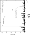
- FIGs. 3A-3C illustrate examples of histogram bin widths
- FIGs. 3A-3C illustrate three equi-width histograms with different bin widths for the same data, with each histogram representing the complete operational region.
- a TDC resolution of 333ps e.g., LSB corresponds to 333ps.
- a histogram with bin width of 1xLSB e.g., bin width 1xLSB/0.33 ns and having 2048 bins
- a strong signal from a physical object at 17m has a distinct peak, as illustrated by 309, however a weaker signal from another physical object at 81m is indistinguishable, as illustrated by 311.
- FIG. 1xLSB e.g., bin width 1xLSB/0.33 ns and having 2048 bins
- 3C in which bin width is set to 64xLSB (e.g., bin width 64xLSB/21.33 ns and having 32 bins), demonstrates a different side effect at the other extreme: if bin width is set too wide, a weak signal is washed out with the noise, as illustrated by 319 (e.g., peak at 81 m) as compared to 317 (e.g., peak at 17 m).
- 64xLSB e.g., bin width 64xLSB/21.33 ns and having 32 bins
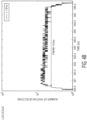
- FIGs. 4A-4B illustrate example pulse shapes of signals. More specifically, FIG. 4A and 4B illustrate a fine resolution (10ps) histogram with a higher number of measurements for target reflections at 17m and 81m, respectively.
- the original signal is a square pulse with full-width at half maximum (FWHM) of 0.5 nanoseconds (ns) and rising and falling times of 0.5ns.
- the FWHM of the target reflection at 17m is around 0.7ns and of 81m is around 5.0ns, e.g., the latter corresponds to the FWHM of original square pulse signal.
- bin width of half of FWHM can be optimal as it ensures at least one bin is fully contained in the FWHM of the detected signal, e.g., maximizes that bin's SNR.
- optimal bin widths for respective physical objects also differ, with 0.35ns or approximately 1xLSB (recall that in LSB is equal to 333ps in the example described above) for the physical object at 17m, and 2.5ns or approximately 8xLSB for the other physical object at 81m.
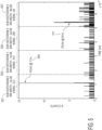
- FIG. 5 illustrates an example of a power-adaptive histogram, in accordance with the present invention.
- the complete operational region is divided into sub-regions each with its independent sub-histogram with a bin width adapted based on signal power.
- bin widths are adjusted relative to signal strength with acquisition cycles, the technique mimics the quality of frequency based histograms for real-time applications, while preserving low maintenance of equi-width histogram.
- the specific histogram illustrated by FIG. 5 has four sub-histograms 501, 503, 505, 507 with bin width of 1, 1, 2, and 8 LSB respectively on the data from FIGs. 3A-3C .
- sub-histogram 0 (e.g., identified as 501) contains 512 bins
- sub-histogram 1 (e.g., identified as 503) contains 512 bins
- sub-histogram 2 (e.g., identified as 505) contains 256 bins
- sub-histogram 3 (e.g., identified as 507) contains 64 bins.
- embodiments are not limited to histograms having four sub-histograms and can include more or less than four sub-histograms.
- the reflection from the physical object at 17m belongs to the sub-histogram 0 with the bin width of 1xLSB and the reflection from the other physical object at 81m (e.g., as illustrated by 511) belongs to the sub-histogram 3 with the bin width of 8xLSB.
- the reflected signal from physical object at 17m is stronger than the one from other physical object at 81m proportionally to the inverse-square of the range. It is worth noting, however, that signals from closer physical objects are not necessarily stronger than the ones from more distant physical objects. For example, an object with reflectivity of 0.8, or 80 percent, at the distance of 50m can result in a stronger reflected signal at the receiver than the object with reflectivity of 0.1, or 10 percent, at the distance of 30m. Therefore, a sub-region containing 50m can have a smaller bin width than the sub-region containing 30m range. Also, note that although for hard targets (as in the above-provided example), the FWHM of reflected signal is limited by FWHM of original transmitted signal, it may not be true for so-called soft targets such as water droplets or glass.
- adaptive histogram is an example of power-adaptive histogram partitioning.
- embodiments are not so limited, and various partitioning of a complete operation region can be performed, based on what is optimal given the number of reflected signals, their strength, memory limitations, etc.
- the finer sub-regions e.g., complete region is divided into higher number of sub-regions
- the histogram is analyzed and the optimal histogram settings for the next acquisition cycle are set, such as: number of sub-regions, boundaries of sub-regions, and bin-widths for each sub-region.
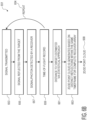
- FIGs. 6A-6B illustrate example methods of using an apparatus. Such methods can be used to simultaneously detect more than one physical objects that are within an operational region, at different sub-regions of the operation region.
- FIG. 6A is an example of a process flow for power-adaptive histogram binning.
- the process 640 includes, at 642, for the first acquisition cycle (e.g., with an acquisition cycle illustrated by 639), the histogram is set up with default parameters: number of sub-histograms, bin widths; memory for sub-histograms is allocated and initialized with zeros.
- TX and RX front-end circuits transmit the signal and measure time-of-flight of the detection (either noise or return signal).
- the sub-histogram that the time-of-flight record 645 hereinafter, time or data record
- the respective sub-histogram is updated by incrementing the corresponding bin.
- the measurements are repeated multiple times, at 641, and the final histogram 649 is complete, at 650.
- the histogram is processed, at 647, and analyzed for optimal histogram setting for the next acquisition cycle, at 643.
- FIG. 6B illustrates an example of a signal flow process of a LIDAR system operated using adaptive binning. As previously described, the process 651 can be used for sensing physical objects located in an operational region.
- the process 651 includes, at 653, transmitting signals by the sensor circuitry (e.g., the TX front-end circuitry). More specifically, at 653, a laser light signal can be transmitted. Thereafter, as depicted at 655, the signal can be reflected from the target lying in the path of the transmitted laser light signal. Then, upon detection of the reflected light as indicated at 657, the time-of-flight can be recorded in a time-of-flight record, as illustrated at 659. Measurements can be repeated multiple times as indicated by the arrow 654 and a statistical approach can be used to identify the actual time-of-flight and as a result, the range to the target, as depicted at 661. That is, the distance to the target can be estimated via a statistical approach, as indicated at 661.
- the sensor circuitry e.g., the TX front-end circuitry
- a step or operation can be implemented as shown thereafter at 663 in which a 2D/3D point cloud of the environment can be generated, at 668.
- Processing of a LIDAR system may extend beyond 2D/3D point cloud generation and can include further filtering of the point cloud (e.g., Kalman filter), segmentation, objects classification and state estimation.
- point cloud can relate to a set of data points in space.
- a point cloud can be used to measure a large number of points on surfaces and of objects around such surfaces.
- a point cloud can also relate to an organized point-cloud map obtained by indexing 3D data to LIDAR-specific 2D coordinate system or vice-versa.
- An example method includes using sensor circuitry to sense and produce detected signals corresponding to physical objects located in the operational region relative to a location of the sensor circuitry.
- the method further includes using processing circuitry operating in response to the detected signals, to record and organize information associated with the detected signals in a plurality of sub-histograms respectively associated with different accuracy metrics for corresponding sub-regions of the operational region, each of the plurality of sub-histograms including a set of histogram bins characterized by a bin width linked to its accuracy metric, and to refine at least one of the accuracy metrics by adapting one or more of the bin widths dynamically in response to the detected signals.
- adapting one or more of the bin widths can include dynamically adapting the bin width of at least one of sub-histograms in response to detected signals in one or more bins.
- the information can be organized in two or more sub-histograms, wherein at least one of the two or more sub-histograms have a different bin width than the other of the two or more sub-histograms.
- the information can be organized in three or more sub-histograms, such as four sub-histograms.
- FIG. 7 illustrates a specific example of sub-histograms with adaptive binning. More specifically, FIG. 7 illustrates an example range-adaptive histogram 775 on the data from FIGs. 3A-3B with the complete operational region divided into sub-regions each with its independent sub-histogram with bin width adapted to the range of the operational region.
- the specific histogram illustrated by FIG. 7 has four sub-histograms 777, 779, 781, 783 with bin widths of 1, 2, 4, and 8 LSB respectively.
- sub-histogram 0 (e.g., identified as 777) contains 512 bins
- sub-histogram 1 (e.g., identified as 779) contains 256 bins
- sub-histogram 2 (e.g., identified as 781) contains 128 bins
- sub-histogram 3 (e.g., identified as 783) contains 64 bins.
- Such exampless are directed to an efficient (fast and cheap) architecture that compensates for the range inverse square power drop, such as those further described herein and illustrated by FIGs. 8A-8B .
- the architecture can be used to efficiently partition the complete operational range into sub-histogram, adjust bin width or bin resolution of each sub-histogram, etc.
- FIGs. 8A-8B illustrate examples of data processing of sub-histograms with range-adaptive binning.
- the bin widths can be adapted to compensate for the range inverse square drop, which is sometimes herein also referred to as a range-adaptive histogram or a range-adaptive application of a power-adaptive histogram binning technique that compensates for range inverse square power drop.
- Such range-adaptive applications can be computationally and memory-wise cheaper and compensates well for the range inverse-square power drop.
- FIG. 8A illustrates an example range-adaptive histogram circuit.
- the range-adaptive histogram circuit can include portions of the processing circuitry 102 illustrated by FIG. 1 .
- bins of all sub-histograms are written in a one single array, e.g. located in a memory. Therefore, hereinafter, the term local bin index, refers to or includes a time record's bin index inside a corresponding sub-histogram's part of the array, and the term global bin index, refers to or includes a time record's bin index inside the complete array.
- the range-adaptive histogram circuit includes a block to perform an operation of retrieving corresponding sub-histogram's first bins global index 867, shift register 860, a storage circuit (e.g., histogram RAM 868), adder 863, among other circuit components such as those illustrated by FIG. 8A (e.g., hist. [indi] ++ 866).
- histogram construction is a non-vectorizable task and cannot be efficiently handled by a digital signal processor, it can be beneficial to have a technique provided with a fast, and simultaneously, inexpensive approach that enables real-time histogram construction in parallel to data acquisition, e.g., histogram is updated immediately as soon as the new time record has arrived.
- histogram is updated immediately as soon as the new time record has arrived.
- the operational region is divided in such a way that only the first M most significant bits (MSBs) of any data record determine the corresponding sub-histogram and the remaining (N - M) bits determine the corresponding bin index inside that sub-histogram, where N is the total number of bits. There may be no overlap between bits determining the sub-histogram and the corresponding local bin index.
- Another simplification is the bin-width to be in the form of 2 ⁇ w x LSB. This way, the time record's local bin index 865 is simply retrieved via right shift of last (N - M) bits by w (hereinafter w is called bin resolution) via the right-shift register 860. This limits the number of possible bin widths, and drastically lowers computational costs.
- Block 862 uses M MSBs to retrieve corresponding sub-histogram's first bin's global index 867 inside complete array. Via adder 863, time records' local bin index 865 and corresponding sub-histogram's first bin global index 867 are used to determine time records' global bin index 861. Corresponding bin is then updated in histogram memory 868.
- the circuitry illustrated by FIG. 8A can have various conditions. First, if the histogram is divided into a large number of sub-histograms, the bin width becomes too wide very quickly (exponential growth) and the signal is washed up by the noise (see FIG. 3C ). As previously described, a bin width that is half of detected signal's FWHM can ensure that at least one bin is fully contained in the FWHM, which can maximize SNR of that bin. For hard physical objects (opposite to soft such as water droplets, glass, etc.), the FWHM of detected signal does not exceed that of the transmitted signal. Since transmitted signal's FWHM is a known parameter, the maximum bin width is limited by half of that amount.
- bin_res represents bin resolution
- w_max is calculated as the closest optimal resolution for the FWHM of transmitted signal.
- Embodiments as described above are directed to generating adaptive histograms having sub-histograms with adaptive bin widths. Bin-widths of the sub-histograms are selected to maximize SNR of detected signals for reliable subsequent peak detection processing, e.g., constant false alarm rate (CFAR). CFAR power of each bin is compared to the local noise power that exclude guard bins surrounding the bin of interest.
- the adaptive histogram technique in accordance with various embodiments, provides a trade-off in a more efficient and computationally cheap manner than potential adaptations in peak detection processing on an equi-width histogram.
- a maximum SNR is ensured, as at least one bin will be fully contained in the FWHM of the signal.
- An equi-width histogram can manifest a possible disadvantage if the guard region is narrow in comparison to detected signal width (e.g., guard bin number is low and/or bin width is narrow), in which case a portion of the signal is included in local noise estimate and this consequently reduces the rate of signal detection. Also, if one selects a wider local noise region to reduce an impact of the detected signal, which can result in delayed and limited response to a local noise change.
- guard region is wide in comparison to detected signal width, then range resolution and/or accuracy is coarser than otherwise physically resolvable; and if a more advanced integration basis is used, (multiplication factor of 1 for current bin, 0.5 for the guard bins right next to it, 0.35 for further, and so on, when estimating current bin power), that can result in higher computing power requirements. Accordingly, aspects disclosed herein account for each of these factors or conditions and provide balance on the trade-off between resolution for strong signals and detection reliability for weak signals.
- a power-adaptive histogram can be constructed both in parallel to data acquisition, as well as reconstructed from the equi-width histogram with the narrowest possible bin width (1xLSB).
- an additional process of reconstructing the histogram, with complexity O(N) is added to the processing pipeline.
- the latter may use higher memory capacities to store an original histogram.
- the power-adaptive histogram in case of 16 bits per bin, can use 15,360 bits (per single SPAD pixel), while equi-width histogram with the bin width of 1xLSB can use 32.768 bit. More than double memory savings is achieved when power-adaptive histogram is constructed in parallel to data acquisition.
- bin index can be retrieved via simple shift operation (w cycles).
- Sub-histograms are predefined to compensate for range inverse-square power drop.
- the sub-histogram of the data record, as well as the pointer to the first bin in the memory is retrieved via set of simple arithmetic operations on M most significant bits.
- circuits or circuitry which may be illustrated as or using terms such as blocks, modules, device, system, unit, controller, and/or other circuit-type depictions (e.g., reference numerals 106 and 234 of FIGs. 1-2 depict a block/module as described herein).
- circuits or circuitry are used together with other elements to exemplify how certain embodiments may be carried out in the form or structures, steps, functions, operations, activities, etc.
- one or more modules are discrete logic circuits or programmable logic circuits configured and arranged for carrying out these operations/activities, as may be carried out in the approaches shown in FIGs.
- such a programmable circuit is one or more computer circuits, including memory circuitry for storing and accessing a program to be executed as a set (or sets) of instructions (and/or to be used as configuration data to define how the programmable circuit is to perform), and an algorithm or process as described at FIGs. 6A-6B is used by the programmable circuit to perform the related steps, functions, operations, activities, etc.
- the instructions (and/or configuration data) can be implemented using logic circuitry, with the instructions (whether characterized in the form of object code, firmware, or software) stored in and accessible from a memory (circuit).
Landscapes
- Physics & Mathematics (AREA)
- Engineering & Computer Science (AREA)
- Electromagnetism (AREA)
- Computer Networks & Wireless Communication (AREA)
- General Physics & Mathematics (AREA)
- Radar, Positioning & Navigation (AREA)
- Remote Sensing (AREA)
- Optical Radar Systems And Details Thereof (AREA)
Claims (11)
- Appareil (100), comprenant :une circuiterie de capteurs (104) configurée et agencée pour produire et détecter des signaux détectés correspondant à des objets physiques dans une région de fonctionnement relative à un emplacement de la circuiterie de capteurs (104) ; etune circuiterie de traitement (102) configurée et agencée pourenregistrer et organiser des informations associées aux signaux détectés dans une pluralité de sous-histogrammes (501, 503, 505, 507) associés respectivement à différentes mesures de précision pour des sous-régions correspondantes de la région de fonctionnement, chacun de la pluralité de sous-histogrammes (501, 503, 505, 507) comportant un ensemble de classes d'histogramme caractérisées par une largeur de classe liée à sa mesure de précision ; etaffiner au moins une des différentes mesures de précision en adaptant dynamiquement une ou plusieurs des largeurs de classes en réponse à une puissance de signal des signaux détectés, caractérisé en ce que chacune des une ou plusieurs largeurs de classes est optimisée à la largeur à mi-hauteur, FWHM, d'un signal détecté correspondant.
- Appareil (100) selon la revendication 1, l'au moins une mesure de précision indiquant une fiabilité de détection, et la circuiterie de capteurs (104) étant configurée et agencée pour mesurer un temps de vol en détectant des signaux optiques et la circuiterie de traitement (102) étant configurée et agencée pour déterminer simultanément une distance de deux objets physiques ou plus (219) depuis la circuiterie de capteurs en utilisant la pluralité de sous-histogrammes (501, 503, 505, 507) avec les une ou plusieurs largeurs de classes adaptées.
- Appareil (100) selon l'une quelconque des revendications précédentes, l'au moins une mesure de précision indiquant un niveau de résolution, et la pluralité de sous-histogrammes (501, 503, 505, 507) correspondant à différentes sous-régions de la région de fonctionnement.
- Appareil (100) selon l'une quelconque des revendications précédentes, comportant en outre une automobile à laquelle la circuiterie de capteurs (104) et la circuiterie de traitement (102) sont fixées, et pendant un mouvement de l'automobile, la circuiterie de capteurs (104) étant en outre configurée et agencée pour produire dynamiquement les signaux détectés et en réponse, la circuiterie de traitement (102) étant en outre configurée et agencée pour affiner dynamiquement l'au moins une mesure de précision pour au moins un de la pluralité de sous-histogrammes (501, 503, 505, 507) en adaptant sa largeur de classe.
- Appareil (100) selon l'une quelconque des revendications précédentes, la pluralité de sous-histogrammes (501, 503, 505, 507) correspondant à différentes sous-régions de la région de fonctionnement avec chacune des différentes sous-régions couvrant une plage différente indiquée par une distance entre la circuiterie de capteurs (104) et un ou plusieurs des objets physiques (219).
- Appareil (100) selon l'une quelconque des revendications précédentes, la circuiterie de traitement (102) étant en outre configurée et agencée pour affiner l'au moins une mesure de précision en fonction d'au moins une indication de puissance détectée dans des signaux reçus optiquement, et d'une indication de distance entre la circuiterie de capteurs (104) et un ou plusieurs des objets physiques (219).
- Appareil selon l'une quelconque des revendications précédentes, la circuiterie de traitement étant en outre configurée et agencée pour faciliter une fiabilité de détection en fonction d'un rapport signal sur bruit, SNR, des signaux détectés, afin de traiter une détection de crête des signaux détectés, au moins une des largeurs de classes étant ajustée en tant qu'étape itérative pour améliorer la détection de crête.
- Appareil selon l'une quelconque des revendications précédentes, la circuiterie de traitement (102) étant en outre configurée et agencée pour fournir des indications de puissance pour les signaux détectés dans chaque ensemble de classes d'histogrammes, et pour affiner l'au moins une mesure de précision en ajustant la largeur de classe sur la base de données empiriques indiquant une correspondance entre des largeurs de classes et une puissance de signal détecté.
- Appareil selon l'une quelconque des revendications précédentes, la circuiterie de traitement (102) étant en outre configurée et agencée pour générer la pluralité de sous-histogrammes, en fonction de données empiriques indiquant une correspondance entre des largeurs de classes et la puissance de signal détecté, les données empiriques étant fournies par un circuit de stockage (108) intégré à la circuiterie de traitement.
- Appareil selon l'une quelconque des revendications précédentes, la circuiterie de traitement (102) étant en outre configurée et agencée pour générer les ensembles de classes d'histogrammes, en fonction de données empiriques indiquant une correspondance entre des largeurs de classes et la puissance de signal détecté, les données empiriques étant reçues en provenance d'un canal de communications fourni par un circuit externe.
- Procédé de détection d'objets physiques (219) situés dans une région de fonctionnement, le procédé comprenant :l'utilisation d'une circuiterie de capteurs (104) pour détecter et produire (644) des signaux détectés correspondant à des objets physiques situés dans la région de fonctionnement relative à un emplacement de la circuiterie de capteurs ; etl'utilisation d'une circuiterie de traitement (102) fonctionnant en réponse aux signaux détectés pour enregistrer et organiser (646, 648) des informations associées aux signaux détectés dans une pluralité de sous-histogrammes (501, 503, 505, 507) associés respectivement à différentes mesures de précision pour des sous-régions correspondantes de la région de fonctionnement, chacun de la pluralité de sous-histogrammes comportant un ensemble de classes d'histogramme caractérisées par une largeur de classe liée à sa mesure de précision; etaffiner (650, 647) au moins une des différentes mesures de précision en adaptant dynamiquement une ou plusieurs des largeurs de classes en réponse à une puissance de signal des signaux détectés, caractérisé en ce que chacune des une ou plusieurs largeurs de classes est optimisée à la largeur à mi-hauteur, FWHM, d'un signal détecté correspondant.
Applications Claiming Priority (1)
| Application Number | Priority Date | Filing Date | Title |
|---|---|---|---|
| US16/253,083 US11656342B2 (en) | 2019-01-21 | 2019-01-21 | Histogram-based signal detection with sub-regions corresponding to adaptive bin widths |
Publications (2)
| Publication Number | Publication Date |
|---|---|
| EP3690475A1 EP3690475A1 (fr) | 2020-08-05 |
| EP3690475B1 true EP3690475B1 (fr) | 2024-11-27 |
Family
ID=69172751
Family Applications (1)
| Application Number | Title | Priority Date | Filing Date |
|---|---|---|---|
| EP20152054.1A Active EP3690475B1 (fr) | 2019-01-21 | 2020-01-15 | Détection de signal basée sur des histogrammes avec des sous-régions avec des compartiments adaptés |
Country Status (3)
| Country | Link |
|---|---|
| US (1) | US11656342B2 (fr) |
| EP (1) | EP3690475B1 (fr) |
| CN (1) | CN111538020B (fr) |
Families Citing this family (23)
| Publication number | Priority date | Publication date | Assignee | Title |
|---|---|---|---|---|
| CN110622038B (zh) * | 2017-05-15 | 2023-04-21 | 夏普株式会社 | 光传感器、电子设备、运算装置及对光传感器与检测对象物之间的距离进行测量的方法 |
| US11733384B2 (en) | 2019-02-20 | 2023-08-22 | Samsung Electronics Co., Ltd. | Single pass peak detection in LIDAR sensor data stream |
| JP7115402B2 (ja) * | 2019-04-10 | 2022-08-09 | 株式会社デンソー | レーダ装置 |
| CN114467038B (zh) | 2019-10-10 | 2025-12-09 | 奥斯特公司 | 处理lidar准确度的时间序列测量 |
| US11644551B2 (en) * | 2020-03-30 | 2023-05-09 | Semiconductor Components Industries, Llc | Lidar systems with improved time-to-digital conversion circuitry |
| US11644553B2 (en) * | 2020-04-17 | 2023-05-09 | Samsung Electronics Co., Ltd. | Detection of reflected light pulses in the presence of ambient light |
| CN112255637B (zh) * | 2020-09-08 | 2024-03-12 | 奥诚信息科技(上海)有限公司 | 距离测量系统及方法 |
| US20220091239A1 (en) * | 2020-09-24 | 2022-03-24 | Nxp B.V. | Photon-based target detection using coarse and fine binning |
| US20240004070A1 (en) * | 2020-11-30 | 2024-01-04 | Hokuyo Automatic Co., Ltd. | Optical rangefinder and optical rangefinding method |
| CN113791422B (zh) * | 2020-12-04 | 2024-04-09 | 神盾股份有限公司 | 飞时测距装置以及飞时测距方法 |
| EP4016124B1 (fr) | 2020-12-16 | 2025-06-04 | Nxp B.V. | Calcul de temps de vol avec estimation delta inter-bin |
| CN114721014B (zh) * | 2021-01-06 | 2025-03-14 | 千寻位置网络有限公司 | 区域电离层改正数的完好性监测方法和装置 |
| JP2022135351A (ja) * | 2021-03-05 | 2022-09-15 | パイオニア株式会社 | 情報処理装置、情報処理方法、プログラム及び記憶媒体 |
| EP4063899A1 (fr) * | 2021-03-25 | 2022-09-28 | Stmicroelectronics Sa | Filtre anti-scintillement pour capteur dtof |
| CN115616521A (zh) * | 2021-07-16 | 2023-01-17 | 上海禾赛科技有限公司 | 用于激光雷达的数据处理方法及激光雷达 |
| US12405376B2 (en) | 2021-07-27 | 2025-09-02 | Samsung Electronics Co., Ltd. | SPAD image sensor |
| US20230090199A1 (en) * | 2021-09-21 | 2023-03-23 | Continental Automotive Systems, Inc. | Lidar system detection compression based on object distance |
| CN114167384B (zh) * | 2021-09-22 | 2024-12-17 | 深圳阜时科技有限公司 | 一种光发射功率调整方法 |
| CN115902835B (zh) * | 2021-09-30 | 2024-02-27 | 深圳市速腾聚创科技有限公司 | 一种雷达数据收发装置、测距方法及激光雷达 |
| WO2023147143A1 (fr) * | 2022-01-30 | 2023-08-03 | Ouster, Inc. | Sous-plages se chevauchant avec pas de puissance |
| JPWO2023181881A1 (fr) * | 2022-03-22 | 2023-09-28 | ||
| US20240094359A1 (en) * | 2022-09-16 | 2024-03-21 | Huawei Technologies Co., Ltd. | Iterative histogram binwidth optimization method for a lidar system and lidar system implementing same |
| WO2025260033A1 (fr) * | 2024-06-14 | 2025-12-18 | Portland State University | Systèmes et procédés de détection tridimensionnelle avec caméras à photon unique pour applications à ressources limitées |
Family Cites Families (5)
| Publication number | Priority date | Publication date | Assignee | Title |
|---|---|---|---|---|
| DE102014116452B4 (de) | 2014-11-11 | 2022-10-27 | Infineon Technologies Ag | Verfahren und Vorrichtung zur Verarbeitung von Radarsignalen |
| US9502458B2 (en) | 2015-03-10 | 2016-11-22 | Stmicroelectronics (Research & Development) Limited | Circuit for generating direct timing histogram data in response to photon detection |
| US10620300B2 (en) | 2015-08-20 | 2020-04-14 | Apple Inc. | SPAD array with gated histogram construction |
| WO2018125438A2 (fr) * | 2016-11-30 | 2018-07-05 | Blackmore Sensors and Analytics Inc. | Procédé et système de balayage adaptatif avec des systèmes de télémétrie optique |
| JP6799690B2 (ja) * | 2017-01-25 | 2020-12-16 | アップル インコーポレイテッドApple Inc. | 変調感度を有するspad検出器 |
-
2019
- 2019-01-21 US US16/253,083 patent/US11656342B2/en active Active
-
2020
- 2020-01-09 CN CN202010034995.9A patent/CN111538020B/zh active Active
- 2020-01-15 EP EP20152054.1A patent/EP3690475B1/fr active Active
Also Published As
| Publication number | Publication date |
|---|---|
| US11656342B2 (en) | 2023-05-23 |
| EP3690475A1 (fr) | 2020-08-05 |
| CN111538020A (zh) | 2020-08-14 |
| US20200233066A1 (en) | 2020-07-23 |
| CN111538020B (zh) | 2025-05-06 |
Similar Documents
| Publication | Publication Date | Title |
|---|---|---|
| EP3690475B1 (fr) | Détection de signal basée sur des histogrammes avec des sous-régions avec des compartiments adaptés | |
| JP7392067B2 (ja) | ライダーのための正確な光検出器測定 | |
| US11175404B2 (en) | Lidar system and method of operating the lidar system comprising a gating circuit range-gates a receiver based on a range-gating waveform | |
| EP4025934B1 (fr) | Traitement d'images lidar | |
| US9383200B2 (en) | Optoelectronic sensor and method for the detection and determination of distances of objects | |
| KR102915686B1 (ko) | Lidar 시스템의 시간적 지터 | |
| CN105043539B (zh) | 用于运行光电探测器的方法和装置 | |
| EP4016124B1 (fr) | Calcul de temps de vol avec estimation delta inter-bin | |
| KR20220145845A (ko) | 솔리드 스테이트 LiDAR용 잡음 필터링 시스템 및 방법 | |
| US20220057520A1 (en) | Distance measurement apparatus and distance measurement method | |
| EP3987305B1 (fr) | Architecture de capteur de profondeur à temps de vol direct et procédé de fonctionnement dudit capteur | |
| KR20230147212A (ko) | 잡음 적응형 솔리드-스테이트 lidar 시스템 | |
| US20240248181A1 (en) | Methods and devices for peak signal detection | |
| EP4198569A1 (fr) | Dispositif lidar, système et procédé | |
| US20240210532A1 (en) | Optoelectronic device with time-of-flight sensor using dynamic time windows | |
| EP4575567A1 (fr) | Dispositif de capteur, dispositif lidar et leur procédé de commande | |
| CN119644354A (zh) | 激光雷达的数据处理方法、激光雷达、终端设备和介质 | |
| US20220381918A1 (en) | Lidar sensor histogram computation | |
| CN111521991B (zh) | 接近检测设备和方法 | |
| WO2025056695A1 (fr) | Circuit, dispositif électronique et procédé d'estimation de profondeur basé sur un temps de vol direct |
Legal Events
| Date | Code | Title | Description |
|---|---|---|---|
| PUAI | Public reference made under article 153(3) epc to a published international application that has entered the european phase |
Free format text: ORIGINAL CODE: 0009012 |
|
| STAA | Information on the status of an ep patent application or granted ep patent |
Free format text: STATUS: THE APPLICATION HAS BEEN PUBLISHED |
|
| AK | Designated contracting states |
Kind code of ref document: A1 Designated state(s): AL AT BE BG CH CY CZ DE DK EE ES FI FR GB GR HR HU IE IS IT LI LT LU LV MC MK MT NL NO PL PT RO RS SE SI SK SM TR |
|
| AX | Request for extension of the european patent |
Extension state: BA ME |
|
| STAA | Information on the status of an ep patent application or granted ep patent |
Free format text: STATUS: REQUEST FOR EXAMINATION WAS MADE |
|
| 17P | Request for examination filed |
Effective date: 20210205 |
|
| RBV | Designated contracting states (corrected) |
Designated state(s): AL AT BE BG CH CY CZ DE DK EE ES FI FR GB GR HR HU IE IS IT LI LT LU LV MC MK MT NL NO PL PT RO RS SE SI SK SM TR |
|
| STAA | Information on the status of an ep patent application or granted ep patent |
Free format text: STATUS: EXAMINATION IS IN PROGRESS |
|
| 17Q | First examination report despatched |
Effective date: 20221214 |
|
| GRAP | Despatch of communication of intention to grant a patent |
Free format text: ORIGINAL CODE: EPIDOSNIGR1 |
|
| STAA | Information on the status of an ep patent application or granted ep patent |
Free format text: STATUS: GRANT OF PATENT IS INTENDED |
|
| INTG | Intention to grant announced |
Effective date: 20240719 |
|
| GRAS | Grant fee paid |
Free format text: ORIGINAL CODE: EPIDOSNIGR3 |
|
| GRAA | (expected) grant |
Free format text: ORIGINAL CODE: 0009210 |
|
| STAA | Information on the status of an ep patent application or granted ep patent |
Free format text: STATUS: THE PATENT HAS BEEN GRANTED |
|
| AK | Designated contracting states |
Kind code of ref document: B1 Designated state(s): AL AT BE BG CH CY CZ DE DK EE ES FI FR GB GR HR HU IE IS IT LI LT LU LV MC MK MT NL NO PL PT RO RS SE SI SK SM TR |
|
| REG | Reference to a national code |
Ref country code: GB Ref legal event code: FG4D |
|
| REG | Reference to a national code |
Ref country code: CH Ref legal event code: EP |
|
| REG | Reference to a national code |
Ref country code: IE Ref legal event code: FG4D |
|
| REG | Reference to a national code |
Ref country code: DE Ref legal event code: R096 Ref document number: 602020041904 Country of ref document: DE |
|
| REG | Reference to a national code |
Ref country code: LT Ref legal event code: MG9D |
|
| REG | Reference to a national code |
Ref country code: NL Ref legal event code: MP Effective date: 20241127 |
|
| PG25 | Lapsed in a contracting state [announced via postgrant information from national office to epo] |
Ref country code: HR Free format text: LAPSE BECAUSE OF FAILURE TO SUBMIT A TRANSLATION OF THE DESCRIPTION OR TO PAY THE FEE WITHIN THE PRESCRIBED TIME-LIMIT Effective date: 20241127 Ref country code: IS Free format text: LAPSE BECAUSE OF FAILURE TO SUBMIT A TRANSLATION OF THE DESCRIPTION OR TO PAY THE FEE WITHIN THE PRESCRIBED TIME-LIMIT Effective date: 20250327 Ref country code: PT Free format text: LAPSE BECAUSE OF FAILURE TO SUBMIT A TRANSLATION OF THE DESCRIPTION OR TO PAY THE FEE WITHIN THE PRESCRIBED TIME-LIMIT Effective date: 20250327 |
|
| PG25 | Lapsed in a contracting state [announced via postgrant information from national office to epo] |
Ref country code: FI Free format text: LAPSE BECAUSE OF FAILURE TO SUBMIT A TRANSLATION OF THE DESCRIPTION OR TO PAY THE FEE WITHIN THE PRESCRIBED TIME-LIMIT Effective date: 20241127 Ref country code: NL Free format text: LAPSE BECAUSE OF FAILURE TO SUBMIT A TRANSLATION OF THE DESCRIPTION OR TO PAY THE FEE WITHIN THE PRESCRIBED TIME-LIMIT Effective date: 20241127 |
|
| REG | Reference to a national code |
Ref country code: AT Ref legal event code: MK05 Ref document number: 1746188 Country of ref document: AT Kind code of ref document: T Effective date: 20241127 |
|
| PG25 | Lapsed in a contracting state [announced via postgrant information from national office to epo] |
Ref country code: BG Free format text: LAPSE BECAUSE OF FAILURE TO SUBMIT A TRANSLATION OF THE DESCRIPTION OR TO PAY THE FEE WITHIN THE PRESCRIBED TIME-LIMIT Effective date: 20241127 |
|
| PG25 | Lapsed in a contracting state [announced via postgrant information from national office to epo] |
Ref country code: ES Free format text: LAPSE BECAUSE OF FAILURE TO SUBMIT A TRANSLATION OF THE DESCRIPTION OR TO PAY THE FEE WITHIN THE PRESCRIBED TIME-LIMIT Effective date: 20241127 |
|
| PG25 | Lapsed in a contracting state [announced via postgrant information from national office to epo] |
Ref country code: NO Free format text: LAPSE BECAUSE OF FAILURE TO SUBMIT A TRANSLATION OF THE DESCRIPTION OR TO PAY THE FEE WITHIN THE PRESCRIBED TIME-LIMIT Effective date: 20250227 |
|
| PG25 | Lapsed in a contracting state [announced via postgrant information from national office to epo] |
Ref country code: LV Free format text: LAPSE BECAUSE OF FAILURE TO SUBMIT A TRANSLATION OF THE DESCRIPTION OR TO PAY THE FEE WITHIN THE PRESCRIBED TIME-LIMIT Effective date: 20241127 Ref country code: AT Free format text: LAPSE BECAUSE OF FAILURE TO SUBMIT A TRANSLATION OF THE DESCRIPTION OR TO PAY THE FEE WITHIN THE PRESCRIBED TIME-LIMIT Effective date: 20241127 Ref country code: GR Free format text: LAPSE BECAUSE OF FAILURE TO SUBMIT A TRANSLATION OF THE DESCRIPTION OR TO PAY THE FEE WITHIN THE PRESCRIBED TIME-LIMIT Effective date: 20250228 |
|
| PG25 | Lapsed in a contracting state [announced via postgrant information from national office to epo] |
Ref country code: PL Free format text: LAPSE BECAUSE OF FAILURE TO SUBMIT A TRANSLATION OF THE DESCRIPTION OR TO PAY THE FEE WITHIN THE PRESCRIBED TIME-LIMIT Effective date: 20241127 |
|
| PG25 | Lapsed in a contracting state [announced via postgrant information from national office to epo] |
Ref country code: RS Free format text: LAPSE BECAUSE OF FAILURE TO SUBMIT A TRANSLATION OF THE DESCRIPTION OR TO PAY THE FEE WITHIN THE PRESCRIBED TIME-LIMIT Effective date: 20250227 |
|
| PG25 | Lapsed in a contracting state [announced via postgrant information from national office to epo] |
Ref country code: SM Free format text: LAPSE BECAUSE OF FAILURE TO SUBMIT A TRANSLATION OF THE DESCRIPTION OR TO PAY THE FEE WITHIN THE PRESCRIBED TIME-LIMIT Effective date: 20241127 |
|
| PG25 | Lapsed in a contracting state [announced via postgrant information from national office to epo] |
Ref country code: DK Free format text: LAPSE BECAUSE OF FAILURE TO SUBMIT A TRANSLATION OF THE DESCRIPTION OR TO PAY THE FEE WITHIN THE PRESCRIBED TIME-LIMIT Effective date: 20241127 |
|
| PG25 | Lapsed in a contracting state [announced via postgrant information from national office to epo] |
Ref country code: EE Free format text: LAPSE BECAUSE OF FAILURE TO SUBMIT A TRANSLATION OF THE DESCRIPTION OR TO PAY THE FEE WITHIN THE PRESCRIBED TIME-LIMIT Effective date: 20241127 |
|
| PG25 | Lapsed in a contracting state [announced via postgrant information from national office to epo] |
Ref country code: RO Free format text: LAPSE BECAUSE OF FAILURE TO SUBMIT A TRANSLATION OF THE DESCRIPTION OR TO PAY THE FEE WITHIN THE PRESCRIBED TIME-LIMIT Effective date: 20241127 |
|
| PG25 | Lapsed in a contracting state [announced via postgrant information from national office to epo] |
Ref country code: SK Free format text: LAPSE BECAUSE OF FAILURE TO SUBMIT A TRANSLATION OF THE DESCRIPTION OR TO PAY THE FEE WITHIN THE PRESCRIBED TIME-LIMIT Effective date: 20241127 |
|
| PG25 | Lapsed in a contracting state [announced via postgrant information from national office to epo] |
Ref country code: CZ Free format text: LAPSE BECAUSE OF FAILURE TO SUBMIT A TRANSLATION OF THE DESCRIPTION OR TO PAY THE FEE WITHIN THE PRESCRIBED TIME-LIMIT Effective date: 20241127 |
|
| PG25 | Lapsed in a contracting state [announced via postgrant information from national office to epo] |
Ref country code: IT Free format text: LAPSE BECAUSE OF FAILURE TO SUBMIT A TRANSLATION OF THE DESCRIPTION OR TO PAY THE FEE WITHIN THE PRESCRIBED TIME-LIMIT Effective date: 20241127 |
|
| P01 | Opt-out of the competence of the unified patent court (upc) registered |
Free format text: CASE NUMBER: APP_29830/2025 Effective date: 20250623 |
|
| REG | Reference to a national code |
Ref country code: DE Ref legal event code: R097 Ref document number: 602020041904 Country of ref document: DE |
|
| REG | Reference to a national code |
Ref country code: CH Ref legal event code: PL |
|
| PG25 | Lapsed in a contracting state [announced via postgrant information from national office to epo] |
Ref country code: SE Free format text: LAPSE BECAUSE OF FAILURE TO SUBMIT A TRANSLATION OF THE DESCRIPTION OR TO PAY THE FEE WITHIN THE PRESCRIBED TIME-LIMIT Effective date: 20241127 |
|
| PG25 | Lapsed in a contracting state [announced via postgrant information from national office to epo] |
Ref country code: LU Free format text: LAPSE BECAUSE OF NON-PAYMENT OF DUE FEES Effective date: 20250115 Ref country code: MC Free format text: LAPSE BECAUSE OF FAILURE TO SUBMIT A TRANSLATION OF THE DESCRIPTION OR TO PAY THE FEE WITHIN THE PRESCRIBED TIME-LIMIT Effective date: 20241127 |
|
| PLBE | No opposition filed within time limit |
Free format text: ORIGINAL CODE: 0009261 |
|
| STAA | Information on the status of an ep patent application or granted ep patent |
Free format text: STATUS: NO OPPOSITION FILED WITHIN TIME LIMIT |
|
| PG25 | Lapsed in a contracting state [announced via postgrant information from national office to epo] |
Ref country code: BE Free format text: LAPSE BECAUSE OF NON-PAYMENT OF DUE FEES Effective date: 20250131 |
|
| PG25 | Lapsed in a contracting state [announced via postgrant information from national office to epo] |
Ref country code: CH Free format text: LAPSE BECAUSE OF NON-PAYMENT OF DUE FEES Effective date: 20250131 |
|
| REG | Reference to a national code |
Ref country code: BE Ref legal event code: MM Effective date: 20250131 |
|
| 26N | No opposition filed |
Effective date: 20250828 |
|
| PGFP | Annual fee paid to national office [announced via postgrant information from national office to epo] |
Ref country code: GB Payment date: 20251220 Year of fee payment: 7 |
|
| PGFP | Annual fee paid to national office [announced via postgrant information from national office to epo] |
Ref country code: FR Payment date: 20251217 Year of fee payment: 7 |
|
| PG25 | Lapsed in a contracting state [announced via postgrant information from national office to epo] |
Ref country code: IE Free format text: LAPSE BECAUSE OF NON-PAYMENT OF DUE FEES Effective date: 20250115 |
|
| PGFP | Annual fee paid to national office [announced via postgrant information from national office to epo] |
Ref country code: DE Payment date: 20251217 Year of fee payment: 7 |