EP3699558A1 - Dispositif émetteur radar pourvu d'antenne intégrée - Google Patents
Dispositif émetteur radar pourvu d'antenne intégrée Download PDFInfo
- Publication number
- EP3699558A1 EP3699558A1 EP19157998.6A EP19157998A EP3699558A1 EP 3699558 A1 EP3699558 A1 EP 3699558A1 EP 19157998 A EP19157998 A EP 19157998A EP 3699558 A1 EP3699558 A1 EP 3699558A1
- Authority
- EP
- European Patent Office
- Prior art keywords
- radar transmitter
- transmitter arrangement
- antenna
- generator
- carrier plate
- Prior art date
- Legal status (The legal status is an assumption and is not a legal conclusion. Google has not performed a legal analysis and makes no representation as to the accuracy of the status listed.)
- Granted
Links
Images



Classifications
-
- G—PHYSICS
- G01—MEASURING; TESTING
- G01F—MEASURING VOLUME, VOLUME FLOW, MASS FLOW OR LIQUID LEVEL; METERING BY VOLUME
- G01F23/00—Indicating or measuring liquid level or level of fluent solid material, e.g. indicating in terms of volume or indicating by means of an alarm
- G01F23/22—Indicating or measuring liquid level or level of fluent solid material, e.g. indicating in terms of volume or indicating by means of an alarm by measuring physical variables, other than linear dimensions, pressure or weight, dependent on the level to be measured, e.g. by difference of heat transfer of steam or water
- G01F23/28—Indicating or measuring liquid level or level of fluent solid material, e.g. indicating in terms of volume or indicating by means of an alarm by measuring physical variables, other than linear dimensions, pressure or weight, dependent on the level to be measured, e.g. by difference of heat transfer of steam or water by measuring the variations of parameters of electromagnetic or acoustic waves applied directly to the liquid or fluent solid material
- G01F23/284—Electromagnetic waves
-
- G—PHYSICS
- G01—MEASURING; TESTING
- G01S—RADIO DIRECTION-FINDING; RADIO NAVIGATION; DETERMINING DISTANCE OR VELOCITY BY USE OF RADIO WAVES; LOCATING OR PRESENCE-DETECTING BY USE OF THE REFLECTION OR RERADIATION OF RADIO WAVES; ANALOGOUS ARRANGEMENTS USING OTHER WAVES
- G01S7/00—Details of systems according to groups G01S13/00, G01S15/00, G01S17/00
- G01S7/02—Details of systems according to groups G01S13/00, G01S15/00, G01S17/00 of systems according to group G01S13/00
- G01S7/03—Details of HF subsystems specially adapted therefor, e.g. common to transmitter and receiver
- G01S7/032—Constructional details for solid-state radar subsystems
-
- G—PHYSICS
- G01—MEASURING; TESTING
- G01S—RADIO DIRECTION-FINDING; RADIO NAVIGATION; DETERMINING DISTANCE OR VELOCITY BY USE OF RADIO WAVES; LOCATING OR PRESENCE-DETECTING BY USE OF THE REFLECTION OR RERADIATION OF RADIO WAVES; ANALOGOUS ARRANGEMENTS USING OTHER WAVES
- G01S13/00—Systems using the reflection or reradiation of radio waves, e.g. radar systems; Analogous systems using reflection or reradiation of waves whose nature or wavelength is irrelevant or unspecified
- G01S13/88—Radar or analogous systems specially adapted for specific applications
-
- H—ELECTRICITY
- H01—ELECTRIC ELEMENTS
- H01Q—ANTENNAS, i.e. RADIO AERIALS
- H01Q1/00—Details of, or arrangements associated with, antennas
- H01Q1/12—Supports; Mounting means
- H01Q1/1207—Supports; Mounting means for fastening a rigid aerial element
-
- H—ELECTRICITY
- H01—ELECTRIC ELEMENTS
- H01Q—ANTENNAS, i.e. RADIO AERIALS
- H01Q1/00—Details of, or arrangements associated with, antennas
- H01Q1/12—Supports; Mounting means
- H01Q1/22—Supports; Mounting means by structural association with other equipment or articles
- H01Q1/225—Supports; Mounting means by structural association with other equipment or articles used in level-measurement devices, e.g. for level gauge measurement
-
- H—ELECTRICITY
- H01—ELECTRIC ELEMENTS
- H01Q—ANTENNAS, i.e. RADIO AERIALS
- H01Q1/00—Details of, or arrangements associated with, antennas
- H01Q1/36—Structural form of radiating elements, e.g. cone, spiral, umbrella; Particular materials used therewith
- H01Q1/38—Structural form of radiating elements, e.g. cone, spiral, umbrella; Particular materials used therewith formed by a conductive layer on an insulating support
-
- H—ELECTRICITY
- H01—ELECTRIC ELEMENTS
- H01Q—ANTENNAS, i.e. RADIO AERIALS
- H01Q15/00—Devices for reflection, refraction, diffraction or polarisation of waves radiated from an antenna, e.g. quasi-optical devices
- H01Q15/02—Refracting or diffracting devices, e.g. lens, prism
Definitions
- the invention relates to sensors for level measurement, for limit level determination and / or for area monitoring.
- the invention relates to a radar transmitter arrangement.
- the invention also relates to a use.
- a level measuring device with a high-frequency front end For process and manufacturing automation, in particular area monitoring, for level measurement or for limit level determination, for example in a container, various types of measuring devices or sensors are used, for example a level measuring device with a high-frequency front end. These measuring devices are used in particular to display a certain level of a product, for example in a container, ie to indicate whether a predefined upper, lower or other limit of the fill level has been reached in the container, or to determine a topology of the product to determine.
- the container can be a vessel or measuring tank of any shape.
- the container can also be a channel, for example a stream or river bed.
- the high-frequency front end is set up to transmit microwaves or radar waves. Many microwave sensors use a radar chip with an integrated antenna.
- a first aspect relates to a radar transmitter arrangement for a sensor for area monitoring, for level measurement or for limit level determination.
- the radar transmitter arrangement has a generator which is set up to generate microwaves, a planar antenna which is connected to the generator and which is set up to transmit the microwaves from the generator, and a carrier plate.
- the generator generates microwaves, for example in a frequency range from 40 to 300 GHz, in particular in a frequency range above 140 GHz, e.g. over 200 GHz.
- An antenna is referred to as a planar antenna which is arranged essentially in one plane with the carrier plate and / or parallel to the carrier plate.
- the planar antenna is arranged essentially perpendicular to a surface normal of the carrier plate.
- the planar antenna has a radiation characteristic which is advantageous for level measurement and / or limit level determination.
- the planar antenna can advantageously be connected to the carrier plate or designed as part of the carrier plate.
- the planar antenna is set up to radiate the microwaves essentially perpendicular to their surface normal. This design achieves radiation of the microwaves in the plane of the carrier plate and / or parallel to the plane of the carrier plate.
- the planar antenna can be arranged on the edge of the carrier plate.
- the printed circuit board can be mounted vertically in the sensor, with a perpendicular orientation of the sensor body. This can lead to better utilization of the space in the sensor.
- this embodiment advantageously enables the sensor to be integrated into certain types and shapes of housings, such as are favorable for level measurement and / or limit level determination or production automation.
- the overall size of the measuring device can thus be reduced, which in at least some cases simplifies the use of such measuring devices and / or expands their range of applications.
- the carrier plate is designed as a printed circuit board.
- the planar antenna can be etched into the circuit board as a structure, for example.
- the generator can be designed as an open or closed chip on the circuit board.
- This chip can, at least in some embodiments, also contain components for controlling and / or evaluating the measurements.
- the chip and / or the circuit board may comprise communication devices, e.g. for wireless and / or wired communication.
- the carrier plate is designed as a semiconductor substrate.
- the generator can be integrated into the semiconductor substrate, for example it can be part of the semiconductor substrate or be arranged on it.
- components for controlling and / or evaluating the measurements and / or communication devices can also be integrated on the semiconductor substrate.
- the planar antenna can be applied to the semiconductor substrate as conductive structures, for example by means of lithography, etched into the semiconductor substrate as a structure, epitaxially and / or produced in some other way. Particularly at high frequencies - for example higher than 100 GHz, in particular at over 200 GHz - the wavelength becomes so small that ⁇ / 4 structures can be implemented directly on a chip.
- the radar transmitter arrangement can be an SMD component (SMD: Surface Mount Device) in a QFN (Quad Flat No Leads Package), BGA (Ball Grid Array) or eWLP (Embedded Wafer Level Ball Grid Array) housing, for example as a "system on Chip "(SoC).
- SMD Surface Mount Device
- QFN Quad Flat No Leads Package
- BGA Bit Grid Array
- eWLP Embedded Wafer Level Ball Grid Array
- SoC System on Chip
- the chip can be configured not to emit the measurement signal on the surface of the chip, but on one of the chip edges. This can e.g. can be achieved by a special antenna arrangement on the chip.
- the planar antenna is implemented as an essentially flat structure on the carrier plate.
- the carrier plate can e.g. be designed as a circuit board or as a semiconductor substrate.
- the wavelength can become so small that ⁇ / 4 structures can be implemented directly on the semiconductor substrate.
- the generator is part of a semiconductor chip.
- the semiconductor chip can also contain further system parts, e.g. for the control and / or evaluation of the measurements, for the communication and / or for the voltage supply of the measuring device.
- the planar antenna is implemented as a Yagi antenna or as a quasi-Yagi antenna.
- this antenna can be implemented as a planar structure on a circuit board or on a chip.
- This structure can e.g. be designed so that it does not radiate from the surface of the chip like other planar structures, but 90 ° from it, i.e. towards one of the long sides of the chip.
- the planar antenna is implemented as a Vivaldi antenna.
- the Vivaldi antenna is combined with another planar antenna, for example a Yagi antenna, for example a first antenna on the front side and a second antenna on a rear side of the carrier plate.
- a narrow emission characteristic can be selected when the fill level is low and a broad emission characteristic when the fill level is high. In this way, the measuring accuracy and / or the energy consumption of the measuring device can be varied over a wide range.
- a variation of the emission characteristic can be used advantageously for the topology detection of a product surface, for example.
- a further planar antenna and / or a further antenna type can be used.
- the radar transmitter arrangement furthermore has a high-frequency lens or dielectric lens, the high-frequency lens being arranged in an emission direction of the planar antenna in order to thereby influence the emission characteristics of the planar antenna.
- the emission characteristic can be changed in such a way as to achieve the narrowest possible emission angle.
- the lenses can e.g. consist of high-density polyethylene (HDPE), PTFE (polytetrafluoroethylene), PEEK (polyetheretherketone) or ceramic and / or have at least one of these materials.
- the radar transmitter arrangement furthermore has a housing within which the radar transmitter arrangement (10) is arranged. Together with the lateral radiation of the radar signal (see above), the circuit board can be mounted vertically in the housing of a sensor and in this way the space can be optimally used.
- the semiconductor material of a radar chip can be mounted, contacted and encapsulated by means of an overmolding on an angled molded part, which can be designed, for example, as an injection molded circuit carrier (MID: Molded Interconnect Device).
- MID Molded Interconnect Device
- an SMD component with a radar transmitter arrangement can be produced by attaching, contacting and overmolding the semiconductor substrate using a 3D-shaped carrier substrate.
- the housing is implemented as a process connection or as part of a process connection. This allows - with relatively little constructive Effort - a robust system can be made available for a wide range of applications.
- a radar transmitter arrangement for a sensor for level measurement or limit level determination which has a generator which is set up to generate microwaves, an antenna which is connected to the generator and which is set up to send the microwaves from the generator, and a carrier plate, wherein the antenna is arranged, by means of an L-shaped angled molded part, essentially perpendicular to a surface normal of the carrier plate and is set up to transmit the microwaves perpendicular to a surface normal.
- the molded part is designed as an SMD component with a radar transmitter arrangement.
- the SMD component can e.g. can be produced by attaching, contacting and overmolding the semiconductor substrate by means of a 3D-shaped carrier substrate.
- the microwaves have a frequency of at least 40 GHz, for example of at least 140 GHz, of at least 200 GHz.
- the radar transmitter arrangement can be integrated, for example, on a semiconductor chip.
- Another aspect relates to the use of a radar transmitter arrangement as described above and / or below for level measurement, for limit level determination and / or for topology detection, for area monitoring and / or for production automation.
- Fig. 1 shows a schematic sketch of a radar transmitter arrangement according to an embodiment in side view.
- the radar transmitter arrangement 10 has a carrier plate 40.
- the carrier plate 40 can be designed, for example, as a printed circuit board or as a semiconductor substrate. Furthermore, a surface normal 45 to the carrier plate 40 is shown.
- a generator 20 is integrated on the carrier plate 40.
- the generator 20 is set up to generate microwaves.
- the semiconductor chip, which comprises the generator 20, can also contain further system parts, eg for the control and / or evaluation of the measurements, for communication and / or for the voltage supply of a measuring device within which the carrier plate 40 is integrated. Further details, such as supply lines to the semiconductor chip, are not shown.
- the carrier plate 40 also has a planar antenna 30 which is connected to the generator 20 via a line 25.
- the planar antenna is placed in the vicinity of an edge 41 of the carrier plate 40.
- the planar antenna 30 is set up to transmit the microwaves from the generator 20 and has a radiation direction or main radiation direction 35, which is outlined by an arrow.
- the planar antenna 30 and the radiation direction 35 are arranged essentially perpendicular to a surface normal 45 of the carrier plate 40.
- the wavelength of the microwaves can be so small that ⁇ / 4 structures or other antenna structures can be implemented directly on the semiconductor substrate 40.
- the carrier substrate 40 can be built into an SMD housing 70 in order to later mount it on a printed circuit board in a standard process (e.g. soldering or gluing).
- the SMD housing has corresponding contact points on the underside.
- Fig. 2a and 2 B show schematic sketches of a radar transmitter arrangement 10 according to a further embodiment in side view. Same reference numbers as for Fig. 1 denote the same or similar elements.
- the radar transmitter arrangement 10 is advantageously arranged in a housing 60, which can be part of a sensor or measuring device. In this way, the space in the housing 60 can be used optimally.
- the planar antenna 30 is placed in the vicinity of an edge of the carrier plate 40 or, in an alternative embodiment, the printed circuit board 75 and that the microwaves or the radar signal are emitted laterally in the direction of a lens 50.
- the exemplary embodiment also shows the high-frequency lens 50, which contribute to the bundling of the microwaves and can thus achieve a narrow radiation angle. This can be particularly advantageous for long measuring distances, for example to measure the fill level, level and / or the surface topology in a large container or measuring tank or above a river bed.
- FIG. 2b the embodiment is off Fig. 1 installed as an SMD component 10 on a circuit board 75 in a sensor housing 60.
- the radiation takes place as in the exemplary embodiment from Fig. 2a .
- the housing 60 shown can also be implemented as a process connection or as part of a process connection.
- the termination area 65 on the process side can be designed to be particularly robust against thermal, mechanical and / or chemical materials. As a result, a robust system for a wide range of applications can be made available - with relatively little construction effort.
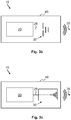
- Fig. 3a shows a schematic sketch of a radar transmitter arrangement 10 according to an embodiment in plan view (along the surface normal 45).
- the radar transmitter arrangement 10 has a carrier plate 40.
- the carrier plate 40 can be designed, for example, as a printed circuit board or as a semiconductor substrate.
- a generator 20 and a planar antenna 30 are arranged on the carrier plate 40.
- the generator 20 and the planar antenna 30 are connected via a line 25.
- the planar antenna 30 is designed as a so-called Yagi antenna.
- the Yagi antenna is placed near one edge of the support plate 40.
- the Yagi antenna 30 is set up to transmit the microwaves from the generator 20 and has a radiation direction or main radiation direction 35, which is represented by an arrow.
- FIG. 3b shows a schematic sketch of a radar transmitter arrangement 10 according to a further embodiment in plan view. Same reference numbers as for Fig. 3a denote the same or similar elements.
- the planar antenna 30 is designed as a so-called quasi-Yagi antenna.
- FIG. 3c shows a schematic sketch of a radar transmitter arrangement 10 according to a further embodiment in plan view. Same reference numbers as for Fig. 3a denote the same or similar elements.
- the planar antenna 30 is designed as a so-called Vivaldi antenna.
- Fig. 4 shows a schematic sketch of a radar transmitter arrangement 11 according to a further embodiment in side view.
- the radar transmitter arrangement 11 has a carrier plate 40.
- a generator 20 in the form of a semiconductor chip is arranged on the carrier plate 40.
- the generator 20 is for generating microwaves set up.
- an antenna 31 is arranged on the carrier plate 40.
- the antenna 31 is designed as a planar antenna, which has a main radiation direction 35 in the direction of its surface normal.
- the antenna 31 is connected to the generator 20 via the line 25 and is set up to transmit the microwaves from the generator 20.
- the antenna can be a patch antenna, for example.
- Both the carrier plate 40 and the antenna 31 are arranged essentially perpendicular to the circuit board 75 by means of an L-shaped angled molded part 80.
- the L-shaped angled molded part 80 can be designed, for example, as an injection-molded circuit carrier (MID: Molded Interconnect Device).
- MID Molded Interconnect Device
- the MID can be assembled, contacted and housed by means of an extrusion coating 70.
- the housed component can have a lens 50 for further focusing the emitted microwave signal.
Landscapes
- Physics & Mathematics (AREA)
- Engineering & Computer Science (AREA)
- Radar, Positioning & Navigation (AREA)
- Remote Sensing (AREA)
- General Physics & Mathematics (AREA)
- Electromagnetism (AREA)
- Computer Networks & Wireless Communication (AREA)
- Thermal Sciences (AREA)
- Fluid Mechanics (AREA)
- Radar Systems Or Details Thereof (AREA)
Priority Applications (4)
| Application Number | Priority Date | Filing Date | Title |
|---|---|---|---|
| EP19157998.6A EP3699558B1 (fr) | 2019-02-19 | 2019-02-19 | Dispositif émetteur radar avec une antenne intégrée |
| US17/427,809 US12345831B2 (en) | 2019-02-19 | 2020-02-19 | Radar transmitter assembly having an integrated antenna |
| CN202080012836.7A CN113412412A (zh) | 2019-02-19 | 2020-02-19 | 具有集成天线的雷达发射器组件 |
| PCT/EP2020/054335 WO2020169655A1 (fr) | 2019-02-19 | 2020-02-19 | Dispositif émetteur radar comprenant une antenne intégrée |
Applications Claiming Priority (1)
| Application Number | Priority Date | Filing Date | Title |
|---|---|---|---|
| EP19157998.6A EP3699558B1 (fr) | 2019-02-19 | 2019-02-19 | Dispositif émetteur radar avec une antenne intégrée |
Publications (2)
| Publication Number | Publication Date |
|---|---|
| EP3699558A1 true EP3699558A1 (fr) | 2020-08-26 |
| EP3699558B1 EP3699558B1 (fr) | 2026-04-01 |
Family
ID=65494024
Family Applications (1)
| Application Number | Title | Priority Date | Filing Date |
|---|---|---|---|
| EP19157998.6A Active EP3699558B1 (fr) | 2019-02-19 | 2019-02-19 | Dispositif émetteur radar avec une antenne intégrée |
Country Status (4)
| Country | Link |
|---|---|
| US (1) | US12345831B2 (fr) |
| EP (1) | EP3699558B1 (fr) |
| CN (1) | CN113412412A (fr) |
| WO (1) | WO2020169655A1 (fr) |
Families Citing this family (2)
| Publication number | Priority date | Publication date | Assignee | Title |
|---|---|---|---|---|
| EP3971611A1 (fr) * | 2020-09-17 | 2022-03-23 | VEGA Grieshaber KG | Appareil de mesure radar |
| US20240195077A1 (en) * | 2022-12-12 | 2024-06-13 | California Institute Of Technology | All-integrated photonic transceiver with a common aperture |
Citations (5)
| Publication number | Priority date | Publication date | Assignee | Title |
|---|---|---|---|---|
| DE4443055A1 (de) * | 1994-12-05 | 1996-06-20 | Grieshaber Vega Kg | Antenneneinrichtung für ein Füllstandmeß-Radargerät |
| DE10051025A1 (de) * | 2000-10-14 | 2002-04-18 | Endress Hauser Gmbh Co | Vorrichtung zur Bestimmung des Füllstands eines Füllguts in einem Behälter |
| US20130016023A1 (en) * | 2005-09-21 | 2013-01-17 | Gaucher Brian P | Apparatus and methods for packaging antennas with integrated circuit chips for millimeter wave applications |
| DE102012112218A1 (de) * | 2012-12-13 | 2014-07-10 | Endress + Hauser Gmbh + Co. Kg | Füllstandsmessgerät |
| US20170211963A1 (en) * | 2014-07-21 | 2017-07-27 | Omid TAHERI | Methods and system for determining pulse temporal coordinates overlapping pulses in a reflected radar signal |
Family Cites Families (13)
| Publication number | Priority date | Publication date | Assignee | Title |
|---|---|---|---|---|
| US5285212A (en) * | 1992-09-18 | 1994-02-08 | Radiation Systems, Inc. | Self-supporting columnar antenna array |
| DE4321411C1 (de) * | 1993-06-26 | 1994-11-10 | Ant Nachrichtentech | Symmetrierschaltung |
| EP1529198B1 (fr) * | 2002-08-13 | 2020-02-26 | VEGA Grieshaber KG | Systeme pour realiser un dispositif de structure modulaire qui sert a determiner une grandeur de processus physique, et composants normalises |
| DE10311040A1 (de) * | 2003-03-13 | 2004-10-07 | Kathrein-Werke Kg | Antennenanordnung |
| US9857475B2 (en) * | 2008-09-09 | 2018-01-02 | Geooptics, Inc. | Cellular interferometer for continuous earth remote observation (CICERO) |
| DE102012016120B4 (de) * | 2012-08-15 | 2017-12-07 | Krohne Messtechnik Gmbh | Mikrowellenfenster und nach dem Radar-Prinzip arbeitendes Füllstandmesssystem |
| EP2869397B1 (fr) * | 2013-11-05 | 2017-02-01 | VEGA Grieshaber KG | Antenne à cornet pivotante pour un radar de niveau de remplissage |
| DE102014207148A1 (de) | 2014-04-14 | 2015-10-15 | Continental Automotive Gmbh | Antennenplatine für die Oberflächenmontage |
| DE102014014860B3 (de) | 2014-10-06 | 2015-09-17 | Audi Ag | Radarsensoranordnung und Kraftfahrzeug |
| US10305198B2 (en) * | 2015-02-25 | 2019-05-28 | At&T Intellectual Property I, L.P. | Facilitating wireless communications via wireless communication assembly apparatuses |
| DE102017113730A1 (de) * | 2017-06-21 | 2018-12-27 | Infineon Technologies Ag | Radar-frontend mit hf-oszillator-überwachung |
| US11047725B2 (en) * | 2018-04-26 | 2021-06-29 | Rosemount Tank Radar Ab | Radar level gauge system with dielectric antenna |
| DE102018117145A1 (de) * | 2018-07-16 | 2020-01-16 | Balluff Gmbh | Multifeldzonen-Näherungssensor sowie ein Verfahren zur Messung eines Abstands eines Objekts vom Multifeldzonen-Näherungssensor |
-
2019
- 2019-02-19 EP EP19157998.6A patent/EP3699558B1/fr active Active
-
2020
- 2020-02-19 US US17/427,809 patent/US12345831B2/en active Active
- 2020-02-19 CN CN202080012836.7A patent/CN113412412A/zh active Pending
- 2020-02-19 WO PCT/EP2020/054335 patent/WO2020169655A1/fr not_active Ceased
Patent Citations (5)
| Publication number | Priority date | Publication date | Assignee | Title |
|---|---|---|---|---|
| DE4443055A1 (de) * | 1994-12-05 | 1996-06-20 | Grieshaber Vega Kg | Antenneneinrichtung für ein Füllstandmeß-Radargerät |
| DE10051025A1 (de) * | 2000-10-14 | 2002-04-18 | Endress Hauser Gmbh Co | Vorrichtung zur Bestimmung des Füllstands eines Füllguts in einem Behälter |
| US20130016023A1 (en) * | 2005-09-21 | 2013-01-17 | Gaucher Brian P | Apparatus and methods for packaging antennas with integrated circuit chips for millimeter wave applications |
| DE102012112218A1 (de) * | 2012-12-13 | 2014-07-10 | Endress + Hauser Gmbh + Co. Kg | Füllstandsmessgerät |
| US20170211963A1 (en) * | 2014-07-21 | 2017-07-27 | Omid TAHERI | Methods and system for determining pulse temporal coordinates overlapping pulses in a reflected radar signal |
Also Published As
| Publication number | Publication date |
|---|---|
| US12345831B2 (en) | 2025-07-01 |
| CN113412412A (zh) | 2021-09-17 |
| US20220120848A1 (en) | 2022-04-21 |
| EP3699558B1 (fr) | 2026-04-01 |
| WO2020169655A1 (fr) | 2020-08-27 |
Similar Documents
| Publication | Publication Date | Title |
|---|---|---|
| EP3450931B1 (fr) | Couplage d'un guide d'onde pour un radar de niveau de remplissage | |
| EP3696516B1 (fr) | Module radar | |
| WO2014006150A1 (fr) | Couplage étanche au gaz d'un guide d'onde, module haute fréquence, radar de niveau de remplissage et utilisation | |
| EP3361223B1 (fr) | Commutateur de niveau de remplissage et procédé de détection d'un niveau limite de fluide dans uns un récipient | |
| CH703903B1 (de) | Stromsensor. | |
| DE2636999A1 (de) | Verfahren zum beruehrungslosen messen der elektrischen leitfaehigkeit eines plaettchens | |
| EP3492881A1 (fr) | Carte de circuits imprimés pour un appareil de mesure de niveau de remplissage radar pourvue de couplage du guide d'onde | |
| DE112005002578T5 (de) | Antennenvorrichtung zur Füllstandsmessung | |
| DE102012203151A1 (de) | Halbleitermodul mit integrierten antennenstrukturen | |
| EP4047742B1 (fr) | Module de radar | |
| EP3699558A1 (fr) | Dispositif émetteur radar pourvu d'antenne intégrée | |
| EP3949011B1 (fr) | Module radar à puce hyperfréquence | |
| DE3231598A1 (de) | Verfahren und vorrichtung zur elektrischen pruefung von mikroverdrahtungen | |
| DE102015210488A1 (de) | Antennenvorrichtung zum Empfangen von elektromagnetischen Wellen und Verfahren zum Betreiben einer Antennenvorrichtung zum Empfangen von elektromagnetischen Wellen | |
| WO2014090565A1 (fr) | Appareil de mesure du niveau de remplissage | |
| WO2020200882A1 (fr) | Module radar à ailette double | |
| EP2796840A1 (fr) | Convertisseur de modes pour un radar de niveau de remplissage | |
| EP4645590A1 (fr) | Ensemble puce haute fréquence, capteur et procédé de fabrication | |
| DE102015102002A1 (de) | Vorrichtung zur Ermittlung und Überwachung eines Füllstands | |
| WO2025002812A1 (fr) | Dispositif radar de mesure de niveau de remplissage pour détecter des niveaux de remplissage dans des récipients | |
| DE102023206601A1 (de) | Messgerät mit zylinderförmiger Monopolantenne | |
| DE102020131550A1 (de) | Kompaktes Radarmessgerät | |
| EP4293818A1 (fr) | Ensemble antenne permettant d'émettre un signal de mesure haute fréquence d'un capteur de mesure | |
| DE102023131661B4 (de) | Baugruppe für Hochfrequenzfeldgeräte, Hochfrequenzfeldgerät und Messstelle | |
| EP2683023B1 (fr) | Couplage de guide d'ondes, module de haute fréquence, radar de niveau de remplissage et utilisation |
Legal Events
| Date | Code | Title | Description |
|---|---|---|---|
| PUAI | Public reference made under article 153(3) epc to a published international application that has entered the european phase |
Free format text: ORIGINAL CODE: 0009012 |
|
| STAA | Information on the status of an ep patent application or granted ep patent |
Free format text: STATUS: REQUEST FOR EXAMINATION WAS MADE |
|
| 17P | Request for examination filed |
Effective date: 20200624 |
|
| AK | Designated contracting states |
Kind code of ref document: A1 Designated state(s): AL AT BE BG CH CY CZ DE DK EE ES FI FR GB GR HR HU IE IS IT LI LT LU LV MC MK MT NL NO PL PT RO RS SE SI SK SM TR |
|
| AX | Request for extension of the european patent |
Extension state: BA ME |
|
| STAA | Information on the status of an ep patent application or granted ep patent |
Free format text: STATUS: EXAMINATION IS IN PROGRESS |
|
| 17Q | First examination report despatched |
Effective date: 20220208 |
|
| GRAP | Despatch of communication of intention to grant a patent |
Free format text: ORIGINAL CODE: EPIDOSNIGR1 |
|
| STAA | Information on the status of an ep patent application or granted ep patent |
Free format text: STATUS: GRANT OF PATENT IS INTENDED |
|
| RIC1 | Information provided on ipc code assigned before grant |
Ipc: G01F 23/284 20060101AFI20251022BHEP Ipc: G01S 13/88 20060101ALI20251022BHEP Ipc: H01Q 1/12 20060101ALI20251022BHEP Ipc: H01Q 1/22 20060101ALI20251022BHEP |
|
| INTG | Intention to grant announced |
Effective date: 20251031 |
|
| GRAS | Grant fee paid |
Free format text: ORIGINAL CODE: EPIDOSNIGR3 |
|
| GRAA | (expected) grant |
Free format text: ORIGINAL CODE: 0009210 |
|
| STAA | Information on the status of an ep patent application or granted ep patent |
Free format text: STATUS: THE PATENT HAS BEEN GRANTED |
|
| RAP3 | Party data changed (applicant data changed or rights of an application transferred) |
Owner name: VEGA GRIESHABER KG |
|
| AK | Designated contracting states |
Kind code of ref document: B1 Designated state(s): AL AT BE BG CH CY CZ DE DK EE ES FI FR GB GR HR HU IE IS IT LI LT LU LV MC MK MT NL NO PL PT RO RS SE SI SK SM TR |
|
| REG | Reference to a national code |
Ref country code: CH Ref legal event code: F10 Free format text: ST27 STATUS EVENT CODE: U-0-0-F10-F00 (AS PROVIDED BY THE NATIONAL OFFICE) Effective date: 20260401 Ref country code: GB Ref legal event code: FG4D Free format text: NOT ENGLISH |
|
| REG | Reference to a national code |
Ref country code: DE Ref legal event code: R096 Ref document number: 502019014518 Country of ref document: DE |
|
| REG | Reference to a national code |
Ref country code: IE Ref legal event code: FG4D Free format text: LANGUAGE OF EP DOCUMENT: GERMAN |