EP3700185A1 - Informationsverarbeitungsvorrichtung, informationsverarbeitungsverfahren, bildgebendes verfahren, und programm - Google Patents
Informationsverarbeitungsvorrichtung, informationsverarbeitungsverfahren, bildgebendes verfahren, und programm Download PDFInfo
- Publication number
- EP3700185A1 EP3700185A1 EP18867663.9A EP18867663A EP3700185A1 EP 3700185 A1 EP3700185 A1 EP 3700185A1 EP 18867663 A EP18867663 A EP 18867663A EP 3700185 A1 EP3700185 A1 EP 3700185A1
- Authority
- EP
- European Patent Office
- Prior art keywords
- information
- pixel
- pixel output
- unit
- image capturing
- Prior art date
- Legal status (The legal status is an assumption and is not a legal conclusion. Google has not performed a legal analysis and makes no representation as to the accuracy of the status listed.)
- Granted
Links
Images








Classifications
-
- H—ELECTRICITY
- H10—SEMICONDUCTOR DEVICES; ELECTRIC SOLID-STATE DEVICES NOT OTHERWISE PROVIDED FOR
- H10F—INORGANIC SEMICONDUCTOR DEVICES SENSITIVE TO INFRARED RADIATION, LIGHT, ELECTROMAGNETIC RADIATION OF SHORTER WAVELENGTH OR CORPUSCULAR RADIATION
- H10F39/00—Integrated devices, or assemblies of multiple devices, comprising at least one element covered by group H10F30/00, e.g. radiation detectors comprising photodiode arrays
- H10F39/10—Integrated devices
- H10F39/12—Image sensors
- H10F39/18—Complementary metal-oxide-semiconductor [CMOS] image sensors; Photodiode array image sensors
-
- H—ELECTRICITY
- H04—ELECTRIC COMMUNICATION TECHNIQUE
- H04N—PICTORIAL COMMUNICATION, e.g. TELEVISION
- H04N19/00—Methods or arrangements for coding, decoding, compressing or decompressing digital video signals
- H04N19/90—Methods or arrangements for coding, decoding, compressing or decompressing digital video signals using coding techniques not provided for in groups H04N19/10-H04N19/85, e.g. fractals
- H04N19/98—Adaptive-dynamic-range coding [ADRC]
-
- H—ELECTRICITY
- H04—ELECTRIC COMMUNICATION TECHNIQUE
- H04N—PICTORIAL COMMUNICATION, e.g. TELEVISION
- H04N23/00—Cameras or camera modules comprising electronic image sensors; Control thereof
- H04N23/60—Control of cameras or camera modules
-
- H—ELECTRICITY
- H04—ELECTRIC COMMUNICATION TECHNIQUE
- H04N—PICTORIAL COMMUNICATION, e.g. TELEVISION
- H04N23/00—Cameras or camera modules comprising electronic image sensors; Control thereof
- H04N23/70—Circuitry for compensating brightness variation in the scene
-
- H—ELECTRICITY
- H04—ELECTRIC COMMUNICATION TECHNIQUE
- H04N—PICTORIAL COMMUNICATION, e.g. TELEVISION
- H04N23/00—Cameras or camera modules comprising electronic image sensors; Control thereof
- H04N23/95—Computational photography systems, e.g. light-field imaging systems
- H04N23/955—Computational photography systems, e.g. light-field imaging systems for lensless imaging
-
- H—ELECTRICITY
- H04—ELECTRIC COMMUNICATION TECHNIQUE
- H04N—PICTORIAL COMMUNICATION, e.g. TELEVISION
- H04N25/00—Circuitry of solid-state image sensors [SSIS]; Control thereof
- H04N25/40—Extracting pixel data from image sensors by controlling scanning circuits, e.g. by modifying the number of pixels sampled or to be sampled
- H04N25/44—Extracting pixel data from image sensors by controlling scanning circuits, e.g. by modifying the number of pixels sampled or to be sampled by partially reading an SSIS array
- H04N25/441—Extracting pixel data from image sensors by controlling scanning circuits, e.g. by modifying the number of pixels sampled or to be sampled by partially reading an SSIS array by reading contiguous pixels from selected rows or columns of the array, e.g. interlaced scanning
-
- H—ELECTRICITY
- H04—ELECTRIC COMMUNICATION TECHNIQUE
- H04N—PICTORIAL COMMUNICATION, e.g. TELEVISION
- H04N25/00—Circuitry of solid-state image sensors [SSIS]; Control thereof
- H04N25/50—Control of the SSIS exposure
-
- H—ELECTRICITY
- H04—ELECTRIC COMMUNICATION TECHNIQUE
- H04N—PICTORIAL COMMUNICATION, e.g. TELEVISION
- H04N25/00—Circuitry of solid-state image sensors [SSIS]; Control thereof
- H04N25/70—SSIS architectures; Circuits associated therewith
-
- H—ELECTRICITY
- H04—ELECTRIC COMMUNICATION TECHNIQUE
- H04N—PICTORIAL COMMUNICATION, e.g. TELEVISION
- H04N25/00—Circuitry of solid-state image sensors [SSIS]; Control thereof
- H04N25/70—SSIS architectures; Circuits associated therewith
- H04N25/79—Arrangements of circuitry being divided between different or multiple substrates, chips or circuit boards, e.g. stacked image sensors
-
- H—ELECTRICITY
- H10—SEMICONDUCTOR DEVICES; ELECTRIC SOLID-STATE DEVICES NOT OTHERWISE PROVIDED FOR
- H10F—INORGANIC SEMICONDUCTOR DEVICES SENSITIVE TO INFRARED RADIATION, LIGHT, ELECTROMAGNETIC RADIATION OF SHORTER WAVELENGTH OR CORPUSCULAR RADIATION
- H10F39/00—Integrated devices, or assemblies of multiple devices, comprising at least one element covered by group H10F30/00, e.g. radiation detectors comprising photodiode arrays
- H10F39/80—Constructional details of image sensors
- H10F39/803—Pixels having integrated switching, control, storage or amplification elements
Definitions
- Patent Document 1 proposes an image capturing device having a configuration of combining a filter including a diffraction grating and an image capturing element to capture light from an object as a pattern obtained through the filter including the diffraction grating, and reproduce an object image by calculation processing using the pattern resulting from the image capturing. Furthermore, the image capturing element that does not use an image capturing lens is also proposed in Patent Document 2 and Non-Patent Document 1.
- Non-Patent Document 1 M. Salman Asif and four others, “Flatcam: Replacing lenses with masks and computation”, “2015 IEEE International Conference on Computer Vision Workshop (ICCVW)", 2015, pp 663-666
- a first aspect of this technology is an information processing device including: an information compression unit configured to perform compression processing to reduce an amount of data of pixel output information including a plurality of pixel outputs that is output from an image capturing element including the plurality of pixel output units configured to receive object light that enters without passing through any of an image capturing lens and a pinhole, and among the plurality of pixel output units, the pixel outputs of at least two of the pixel output units have incident angle directivity modulated into different incident angle directivity according to an incident angle of the object light.
- the information compression unit performs the compression processing to reduce the amount of data of the pixel output information including a plurality of pixel outputs that is output from the image capturing element.
- the image capturing element includes the plurality of pixel output units configured to receive the object light that enters without passing through any of an image capturing lens and a pinhole, and among the plurality of pixel output units, the pixel outputs of at least two of the pixel output units have incident angle directivity modulated into different incident angle directivity according to the incident angle of the object light.
- the information compression unit classifies, for example, each of the plurality of pixel outputs into one of a plurality of classifications on the basis of the incident angle directivity, and performs the compression processing on each classification.
- the information compression unit computes a difference between reference value information and the pixel outputs as the compression processing.
- the reference value information may be set on the basis of the pixel outputs, or the pixel output immediately before may be set as the reference value information.
- the information compression unit may reduce a word length of the pixel output information by performing linear calculation on a calculation parameter set on the basis of the pixel outputs and the pixel outputs, and the information compression unit discriminates a compression word length of the pixel output information after the compression processing, and controls exposure on the basis of the discriminated compression word length. Furthermore, the information compression unit performs the compression processing for each color component.
- the information processing device may further include an image conversion unit configured to generate a reconstruction image that allows visual recognition of the object by using one of the pixel output information that has undergone the compression processing by the information compression unit, the pixel output information after expansion processing of the pixel output information that has undergone the compression processing, and the pixel output information before the compression processing.
- an image conversion unit configured to generate a reconstruction image that allows visual recognition of the object by using one of the pixel output information that has undergone the compression processing by the information compression unit, the pixel output information after expansion processing of the pixel output information that has undergone the compression processing, and the pixel output information before the compression processing.
- each of the plurality of pixel output units includes one photodiode
- each of the at least two pixel output units includes a light-shielding film that shields incidence of the object light on the photodiode, and a range in which the object light is shielded by the light-shielding film is different from each other between the at least two pixel output units.
- a fifth aspect of this technology is a program for causing a computer to execute image processing and causing the computer to execute a step of reducing an amount of data of pixel output information including a plurality of pixel outputs that is output from an image capturing element including the plurality of pixel output units configured to receive object light that enters without passing through any of an image capturing lens and a pinhole, and among the plurality of pixel output units, the pixel outputs of at least two of the pixel output units have incident angle directivity modulated into different incident angle directivity according to an incident angle of the object light.
- Every object can be considered as a set of point light sources, and light is emitted in all directions. Therefore, the principle of image capturing can be described by considering how to capture light emitted from the point light sources.
- Fig. 1 is a diagram for describing the principle of image capturing in a case where an image capturing lens is used.
- objects on an object plane OP are, for example, point light sources PA, PB, and PC.
- a light beam emitted from the point light source PA is collected at a position Pa on an image capturing plane IP by an image capturing lens LNZ.
- the image capturing lens LNZ is a lens having a light collecting function for causing object light incident from the same direction to enter both pixels adjacent to each other.
- a light beam emitted from the point light source PB (PC) is collected at a position Pb (Pc) on the image capturing plane IP by the image capturing lens LNZ.
- a pixel output according to intensity of the light beam from the point light source PA that penetrates the hole BKH is obtained.
- a pixel output according to intensity of the light beam from the point light source PB (PC) that penetrates the hole BKH is obtained. Therefore, an image signal of a captured image indicating the point light sources PA, PB, and PC on the object plane OP can be generated using the pixel output of each pixel.
- the vertical axis represents the position on the image capturing plane IP
- the horizontal axis is a detected value based on light intensity in the image capturing element at each position.
- (b) of Fig. 2 illustrates a case where the detected value is SDpa at the position Pa, the detected value is SDpb at the position Pb, the detected value is SDpc at the position Pc, and "SDpb > SDpa > SDpc.”
- the pixel output is generated only by the hole BKH and the penetrated light beam, the detected value is smaller than in a case where the image capturing lens is used.
- Fig. 3 is a diagram for describing a case where a normal image capturing element is used with a lens-less configuration including no image capturing lens or pinhole.
- the light beam emitted from each of the point light sources PA, PB, and PC enters positions Qa, Qb, and Qc.
- the vertical axis represents the position in the image capturing plane IP
- the horizontal axis is a detected value based on light intensity in the pixel at each position.
- the pixel output of the element at each of the positions Qa, Qb, and Qc is a pixel output according to the intensity of the light beams from the point light sources PA, PB, and PC.
- (b) of Fig. 3 shows the detected value SDsa at the position Qa, the detected value SDsb at the position Qb, the detected value SDsc at the position Qc, and "SDsa ⁇ SDsb ⁇ SDsc.” Therefore, the image signal of the captured image indicating the point light sources PA, PB, and PC on the object plane OP cannot be generated using the pixel output of each pixel.
- the image capturing unit has a configuration using an image capturing element including a plurality of pixel output units that receives object light that enters without passing through any of an image capturing lens and a pinhole, and among the plurality of pixel output units, output pixels of at least two of the pixel output units have incident angle directivity modulated into different incident angle directivity according to an incident angle of the object light.
- the image capturing element acquires the pixel outputs of one image including the pixel outputs at the positions of respective pixel output units.
- the image capturing unit generates the pixel output for each pixel output unit for the object light that enters without passing through the light-collecting function for causing the object light incident from the same direction to enter both pixel output units adjacent to each other, and the incident angle directivity of the output pixel values (pixel outputs) of at least two pixel output units of the plurality of pixel output units is different. That is, the image capturing unit generates the pixel output for each pixel output unit by the image capturing element of image capturing lens free.
- the image capturing unit generates the pixel output information according to the object light will be described.
- Fig. 4 is a diagram illustrating the configuration of the image capturing unit that generates the pixel output information to be processed by the information processing device of the present technology. Note that Fig. 4 shows a partial region of the image capturing unit, for example, a region in which the number of pixels in the horizontal direction and the vertical direction is 6 pixels ⁇ 6 pixels, respectively.
- a light-shielding film 121b which is a modulation element and a part of a light receiving region of the photodiode, is provided for each pixel 121a as a different range, and incident light that enters each pixel 121a is optically modulated according to the incident angle. That is, the image capturing unit 121 has a configuration that makes it possible to have different light-receiving sensitivity according to the incident angle of incident light for each pixel (pixel output unit), and has directivity with respect to the incident direction, that is, incident angle directivity.
- each pixel 121a has a different light-receiving sensitivity to the incident angle of the incident light, and each pixel 121a has different incident angle directivity.
- the light-shielding film 121b-1 and the light-shielding film 121b-2 provided in the pixel 121a-1 and the pixel 121a-2 respectively have different ranges where light is shielded in the pixels (at least one of the region (position) to shield light and the area to shield light is different). That is, in the pixel 121a-1, the light-shielding film 121b-1 is provided to shield a part of the left side of the light receiving region of the photodiode by a predetermined width.
- FIG. 5 is a diagram showing a configuration example of the image capturing unit 121.
- (a) of Fig. 5 is a side cross-sectional view of the image capturing unit 121.
- (b) of Fig. 5 is a top view of the configuration example of the image capturing unit 121. Note that the side cross-sectional view of (a) of Fig. 5 is an A-B cross section of (b) of Fig. 5 .
- Fig. 5 is a side view and a top view of two pixels constituting the pixel array of the image capturing unit 121. Needless to say, a larger number of pixels 121a are arranged, but are omitted in the diagram.
- the pixels 121a-15 and 121a-16 include photodiodes 121e-15 and 121e-16 in the photoelectric conversion layer Z11, respectively. Furthermore, on-chip lenses 121c-15 and 121c-16, and color filters 121d-15 and 121d-16 are respectively formed from above on the photodiodes 121e-15 and 121e-16.
- the color filters 121d-15 and 121d-16 are filters that transmit light having either specific wavelength such as red, green, blue, and infrared, for example. Furthermore, the color filters 121d-15 and 121d-16 may be transparent, and a configuration that does not use any color filter may be employed.
- Light-shielding films 121b-15 and 121b-16 and an element separation film 121s are formed at a boundary between the pixels in the photoelectric conversion layer Z11 of the pixels 121a-15 and 121a-16.
- the light-shielding films 121b-15 and 121b-16 each have an L-shaped configuration in side view, and include incident light-shielding portions 121b-15a and 121b-16a provided on the filter surface side, and separation portions 121b-15b and 121b-16b formed perpendicularly to the filter surface.
- incident light-shielding portions 121b-15a and 121b-16a provided on the filter surface side
- separation portions 121b-15b and 121b-16b formed perpendicularly to the filter surface.
- the incident light-shielding portions of the light-shielding films 121b-15 and 121b-16 shield a light-receiving plane S viewed from the upper surface.
- the incident light-shielding portions 121b-15a and 121b-16a of the light-shielding films 121b-15 and 121b-16 whereby different incident angle directivity is set for each pixel (pixel output unit).
- the range in which light is shielded is not necessarily different in each of all the pixels 121a of the image capturing unit 121. There may be some pixels 121a in which the same region is shielded from light.
- the element separation film 121s is provided to face the separation portions 121b-15b and 121b-16b of the light-shielding films 121b-15 and 121b-16.
- Crosstalk between adjacent pixels is suppressed by the separation portions of the light-shielding films 121b-15 and 121b-16 and the element separation film 121s, for example, for incident light L in (a) of Fig. 5 .
- the light-shielding films 121b-15 and 121b-16 and the element separation film 121s includes a metal, for example, tungsten (W), aluminum (Al), or an alloy of aluminum (Al) and copper (Cu). Furthermore, the light-shielding films 121b-15 and 121b-16 and the element separation film 121s may be formed simultaneously with the same metal as the wiring by the same process as the wiring forming process in a semiconductor process. Moreover, film thicknesses of the light-shielding films 121b-15 and 121b-16 and the element separation film 121s do not have to be the same thickness depending on the position. Note that in the examples of Figs. 4 and 5 , one pixel corresponds to one pixel output unit.
- Fig. 6 is a diagram showing a second configuration example of the image capturing unit 121.
- (a) of Fig. 6 shows a side cross-sectional view of the pixel 121a of the image capturing unit 121 that is the second configuration example.
- Fig. 6(b) shows a top view of the image capturing unit 121.
- the side cross-sectional view shown in (a) of Fig. 6 is an A-B cross section in (b) of Fig. 6 .
- the image capturing unit 121 has a configuration different from the configuration of the image capturing unit 121 of Fig. 5 in that four photodiodes 121f-1 to 121f-4 are formed in the pixel 121a, and the element separation film 121s is formed in a region separating the photodiodes 121f-1 to 121f-4. That is, in the image capturing unit 121 of Fig. 6 , the element separation film 121s is formed in a "+" shape when viewed from above. The intersection position of the "+" shape may be set at the center position of the pixel 121a as shown in Fig. 6 such that the light-receiving surfaces of the four photodiodes have the same size.
- the pixel 121a may have a configuration including photodiodes having different light-receiving surface sizes, that is, a configuration including pixel output units with different characteristics depending on whether the intersection position is moved or not. Note that common components are denoted with the same reference symbol, and detailed description thereof will be omitted.
- the photodiodes 121f-1 to 121f-4 are separated by the element separation film 121s, thereby preventing electrical and optical crosstalk between the photodiodes 121f-1 to 121f-4.
- the image capturing unit of Fig. 5 has a configuration in which the incident angle directivity of each pixel differs by providing one pixel output unit with one photodiode and making the light-shielding state of each pixel (pixel output unit) by the light-shielding film 121b different for each pixel.
- one pixel corresponds to the pixel output unit.
- four photodiodes are provided in one pixel output unit, and the photodiode that contributes to the output pixel unit among the four photodiodes is different for each pixel output unit, whereby each pixel output unit can be provided (set) with different incident angle directivity independently.
- output pixel information is generated by adding signals obtained by the photodiode 121f-1 and the photodiode 121f-2, the output pixel information has horizontal incident angle directivity. If output pixel information is generated by adding signals obtained by the photodiodes 121f-1 and 121f-3, the output pixel information has vertical incident angle directivity.
- FIG. 7 is a diagram for describing incident angle directivity of the pixel output unit in the image capturing unit 121.
- an on-chip lens 121c-11 (121c-12) that collects incident light from the upper incident direction
- a color filter 121d-11 (121d-12) that transmits light of a predetermined wavelength
- a photodiode 121e-11 (121e-12) that generates a pixel signal by photoelectric conversion are stacked in this order.
- a light-shielding film 121b-11 (121b-12) including, for example, metal wiring and the like and shields a part of the region that receives incident light.
- the detected value of the photodiode 121e-11 increases as the incident angle ⁇ increases (as the incident direction shifts toward the right side in the diagram) because light enters a range where the light-shielding film 121b-11 is not provided.
- the detected value of the photodiode 121e-11 decreases as the incident angle ⁇ decreases (as the incident direction shifts toward the left side in the diagram) because light enters a range where the light-shielding film 121b-11 is provided.
- the detected value of the photodiode 121e-12 decreases as the incident angle ⁇ increases (as the incident direction shifts toward the right side in the diagram) because light enters a range where the light-shielding film 121b-12 is provided. Conversely, the detected value of the photodiode 121e-12 increases as the incident angle ⁇ decreases (as the incident direction shifts toward the left side in the diagram) because light enters a range where the light-shielding film 121b-12 is not provided.
- the waveforms shown by the solid and dotted lines indicating the change in the detected value according to the incident angle ⁇ shown in (c) of Fig. 7 can be changed according to the range of the light-shielding films 121b-11 and 121b-12, thereby making it possible to have incident angle directivity different from each other between the pixel output units.
- the incident angle directivity mentioned here is the characteristic of change in the detected value of each pixel output unit according to the incident angle ⁇ . It can be said that this is a characteristic of the change in the light shielding level according to the incident angle ⁇ . That is, the light-shielding films 121b-11 and 121b-12 shield incident light of a specified direction at a high level, but cannot sufficiently shield incident light from directions other than the specified direction.
- the incident light is optically modulated according to the incident angle, and the change in the level at which light can be shielded causes a change in the detected value according to the incident angle ⁇ as shown in (a) of Fig. 7 . Therefore, it is possible to provide each pixel output unit with different incident angle directivity.
- the configuration of the image capturing unit is not limited to the configuration that provides each pixel output unit with different incident angle directivity by using the light-shielding film that can be set independently for each pixel output unit, changing the number of contributing photodiodes, or changing the intersection position of a plurality of photodiodes.
- the image capturing unit may use a random black and white pattern mask or an optical interference mask as an element for causing the incident angle directivity to have characteristics different from each other.
- Fig. 8 is a diagram showing another configuration of the image capturing unit.
- the image capturing unit 221 has a configuration in which a mask 223 that is a modulation element is fixed to an image capturing element 222 to have a predetermined space with respect to the image capturing plane IP of the image capturing element 222, and light from the object plane OP enters the image capturing plane IP of the image capturing element 222 via the mask 223.
- Fig. 9 is a diagram showing a case where a black and white pattern mask is used.
- (a) of Fig. 9 illustrates the black and white pattern mask.
- the black and white pattern mask 223BW has a configuration in which white pattern parts that transmit light and black pattern parts that shields light are randomly arranged.
- the pattern size is set independently of the pixel size of the image capturing element 222.
- (b) of Fig. 9 schematically shows an irradiation state of the image capturing plane IP with the light emitted from the point light source PA and the light emitted from the point light source PB. Furthermore, (c) of Fig.
- FIG. 9 schematically and individually shows a response of the image capturing element to the light emitted from the point light source PA and the light emitted from the point light source PB in a case where the black and white pattern mask 223BW is used.
- the light from the object plane OP enters the image capturing plane IP of the image capturing element 222 via the black and white pattern mask 223BW. Therefore, the response of the image capturing element to the light emitted from the point light source PA of the object plane OP is Sbwa. Furthermore, the response of the image capturing element to the light emitted from the point light source PB of the object plane OP is Sbwb.
- the pixel output information output from the image capturing element 222 is information of one image obtained by combining the response of each point light source for each pixel output unit.
- the incident angle directivity cannot be set independently for each pixel output unit, and pixel output units at close positions have incident angle directivity close to each other.
- Fig. 10 is a diagram showing a case where an optical interference mask is used.
- the image capturing plane IP of the image capturing element 222 is irradiated with the light emitted from the point light sources PA and PB of the object plane OP via the optical interference mask 223LF.
- the light incident surface of the optical interference mask 223LF is provided with unevenness on a scale of a light wavelength as shown in (b) of Fig. 10 .
- the optical interference mask 223LF has the maximum transmission of light of a specified wavelength emitted from the perpendicular direction.
- an optical filter 223HW of Fig. 11 may be used instead of the optical filter 223BW.
- the optical filter 223HW includes a linear polarizing element 231A and a linear polarizing element 231B having the same polarization direction, and a ⁇ /2 wave plate 232.
- the ⁇ /2 wave plate 232 is sandwiched between the linear polarizing element 231A and the linear polarizing element 831B.
- a polarizing part shown by oblique lines is provided, and the white pattern parts and the polarizing parts are randomly arranged.
- the linear polarizing element 231B transmits the polarized light having penetrated the white pattern part, and hardly transmits the polarized light having penetrated the polarizing part. Therefore, the polarized light having penetrated the polarizing part has a smaller light amount than the polarized light having penetrated the white pattern part. Therefore, a light and shade pattern almost similar to the case where the optical filter 223BW is used can be generated on the light-receiving plane (image capturing plane) IP of the image capturing element 222.
- a light beam emitted from the same point light source enters the image capturing plane IP via elements for causing the incident angle directivity to have characteristics different from each other, and light of incident angle directivity different from each other (for example, light with light intensity according to the difference in the incident angle or mask) enters each pixel output unit of the image capturing plane IP. That is, even the light beam having the same light intensity is detected with different sensitivity by each pixel output unit, and is detected as different detected values by each pixel output unit.
- the difference in the incident angle directivity is expressed by a coefficient
- the detected value according to the incident light in each pixel output unit can be obtained by multiplying the light intensity of the incident light by the coefficient according to the incident angle directivity.
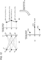
- Fig. 12 is a diagram for describing computation of the detected value and the pixel value according to the incident light in each pixel output unit.
- the image capturing unit 121 captures the point light sources PA, PB, and PC on the object plane OP.
- (b) of Fig. 12 illustrates the relationship between the positions on the image capturing plane and the detected values.
- the detected values SDA, SDB, and SDC at the positions Qa, Qb, and Qc are expressed by the following equations (1) to (3), respectively.
- ⁇ 1 represents the incident angle directivity according to the incident angle of the light beam from the point light source PA at the position Qa of the image capturing plane IP, and is a coefficient corresponding to the light intensity a.
- ⁇ 1 represents the incident angle directivity according to the incident angle of the light beam from the point light source PB of the object plane OP to reconstruct at the position Qa of the image capturing plane IP, and is a coefficient corresponding to the light intensity b.
- ⁇ 1 represents the incident angle directivity according to the incident angle of the light beam from the point light source PC of the object plane OP to reconstruct at the position Qa of the image capturing plane IP, and is a coefficient corresponding to the light intensity c.
- ( ⁇ 1 ⁇ a) of the detected value SDA indicates the detected value by the light beam from the point light source PA at the position Qa, and is obtained by multiplying the light intensity a of the light beam from the point light source PA at the position Qa by the coefficient ⁇ 1 indicating the incident angle directivity according to the incident angle.
- ( ⁇ 1 ⁇ b) of the detected value SDA indicates the detected value by the light beam from the point light source PB at the position Qa, and is obtained by multiplying the light intensity b of the light beam from the point light source PB at the position Qa by the coefficient ⁇ 1 indicating the incident angle directivity according to the incident angle.
- ( ⁇ 1 ⁇ c) of the detected value SDA indicates the detected value by the light beam from the point light source PC at the position Qa, and is obtained by multiplying the light intensity c of the light beam from the point light source PC at the position Qa by the coefficient ⁇ 1 indicating the incident angle directivity according to the incident angle.
- the detected value SDA is expressed as the sum of products of the light intensity a, b, and c of the light beams from the point light sources PA, PB, and PC at the position Qa and the coefficients ⁇ 1, ⁇ 1, and ⁇ 1.
- a set of coefficients used for computing one detected value for example, a set of the coefficients ⁇ 1, ⁇ 1, and ⁇ 1 is defined as a coefficient set.
- the coefficient set " ⁇ 2, ⁇ 2, ⁇ 2" corresponds to the coefficient set " ⁇ 1, ⁇ 1, ⁇ 1" for the detected value SDA at the point light source PA, respectively.
- the coefficient set " ⁇ 3, ⁇ 3, ⁇ 3" corresponds to the coefficient set " ⁇ 1, ⁇ 1, ⁇ 1" for the detected value SDA at the point light source PA, respectively.
- the detected values at the positions Qa, Qb, and Qc are values expressed by the sum of products of the light intensity a, b, c of the light beams emitted from the point light sources PA, PB, and PC and the coefficients, respectively. Therefore, these detected values are mixtures of the light intensity a, b, and c of the light beams emitted from the point light sources PA, PB, and PC, respectively, and thus are different from the image of the object.
- the detected values at the positions Qa, Qb, and Qc are mixtures of the light intensity a, b, and c of the light beams emitted from the point light sources PA, PB, and PC, respectively, the difference in the detected values between respective pixel output units is smaller than in a case where the image capturing lens is used, and the signal level is relatively uniform over the entire screen.
- the detected values of the pixel output units at the positions Qa, Qb, and Qc are, as described above, values expressed by the sum of products of the light intensity a, b, and c of the light beams emitted from the point light sources PA, PB, and PC, respectively, and the coefficients. Therefore, by forming simultaneous equations using the coefficients ⁇ 1, ⁇ 1, ⁇ 1, ⁇ 2, ⁇ 2, ⁇ 2, ⁇ 3, ⁇ 3, and y3 and the detected values SDA, SDB, and SDC and solving the light intensity a, b, and c, in other words, by performing reconstruction calculation using the detected values and the coefficients, as shown in (c) of Fig.
- pixel values GPqa, GPqb, and GPqc at the positions Qa, Qb, and Qc can be obtained, respectively. Furthermore, not only in a case where the image capturing unit 121 is used, but also in a case where the image capturing unit 221 is used, by performing similar processing, the reconstruction calculation using the detected values at the positions Qa, Qb, and Qc and the coefficients is performed, and the pixel values GPqa, GPqb, and GPqc at the positions Qa, Qb, and Qc can be obtained, respectively.
- the plurality of coefficient sets " ⁇ 1, ⁇ 1, ⁇ 1", " ⁇ 2, ⁇ 2, ⁇ 2", and " ⁇ 3, ⁇ 3, ⁇ 3" used in the reconstruction calculation are defined as a coefficient set group.
- the coefficients ⁇ 1, ⁇ 1, ⁇ 1, ⁇ 1, ⁇ 2, ⁇ 2, ⁇ 2, ⁇ 3, ⁇ 3, ⁇ 3 are the coefficient set group for computing the light intensity of the point light sources on the object plane from the pixel outputs.
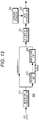
- Fig. 13 is a diagram showing the configuration of the information processing system.
- the information processing system 300 includes an information compression unit 311, a recording unit 312, a reproduction unit 320, an information expansion unit 321, an image conversion unit 322, and a coefficient storage unit 323. Note that the configuration of the information processing system 300 is not limited to the configuration shown in Fig. 13 .
- the information processing system 300 may have a configuration using only some blocks according to the operation to be performed by the information processing system 300.
- the reproduction unit 320 For example, in a case where only processing of outputting the pixel output information with a reduced amount of data from the information processing system 300 to an external device, or processing of recording in a recording medium is performed, it is not necessary to use the reproduction unit 320, the information expansion unit 321, the image conversion unit 322, or the coefficient storage unit 323. Furthermore, in a case where only reproduction processing of the pixel output information with a reduced amount of data is performed, the pixel output information being supplied from an external device or recorded in a recording medium, it is not necessary to use the information compression unit 311 or the recording unit 312.
- the image capturing unit 121 (221) generates the pixel output information according to the incident angle directivity.
- the image capturing unit is similar to, for example, an image capturing element such as a complementary metal oxide semiconductor (CMOS) image sensor, but differs in configuration from the conventional image capturing unit using the image capturing lens in that an element for causing the incident angle directivity to have characteristics different from each other is used.
- CMOS complementary metal oxide semiconductor
- Such a coefficient ⁇ 1 for the point light source PA, the coefficient ⁇ 1 for the point light source PB, and coefficients for other point light sources are computed in advance according to the image capturing unit 121 (221), and the coefficient set group including the coefficient set computed for each position is stored in the coefficient storage unit 323.
- Fig. 14 is a diagram illustrating the configuration of the first embodiment of the information compression unit.
- an information compression unit 311-1 performs differential compression and reduces the amount of data of the pixel output information output from the image capturing unit 121 (221) to allow reduction in the load on storage and transmission of the pixel output information.
- the information compression unit 311-1 includes, for example, a reference setting unit 3111 and a difference calculation unit 3112.
- the reference setting unit 3111 sets the reference value information.
- the difference calculation unit 3112 computes the difference between the reference value information set by the reference setting unit 3111 and the pixel output information of each pixel output unit, thereby generating the compressed information with the amount of data smaller than the pixel output information.
- Fig. 15 is a diagram for describing the first operation.
- the reference setting unit 3111 sets a preset value or an average value of the pixel output information as reference value information DC.
- Fig. 15 is an example in a case where the pixel output information having a bit width (bit depth) of 8 bits is processed.
- Fig. 15 illustrates a case where the average value of the pixel values of all the pixel output units is, for example, "192.”
- all the pixel output units may be, for example, all the pixel output units of an image immediately before recording, all the pixel output units of an image of a live view image at desired timing, and the like.
- all the pixel output units are all the pixel output units of the image to be subjected to compression processing.
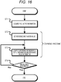
- Fig. 16 is a flowchart showing the first operation.
- the information compression unit acquires the pixel output.
- the information compression unit acquires the pixel output generated by the image capturing unit, and proceeds to step ST2.
- step ST2 the information compression unit sets the reference value information.
- the information compression unit sets the average value, minimum value, maximum value, or fixed value of the pixel values of all the pixel output units as the reference value information, and proceeds to step ST3.
- step ST3 the information compression unit computes the difference between the pixel output and the reference value information.
- the information compression unit computes the difference between the pixel output and the reference value information set in step ST2, uses the computation result as the compressed information, and proceeds to step ST4.
- step ST4 the information compression unit determines whether all the pixels have been finished. In a case where the generation of the compressed information for all the pixel output units has not been completed, the information compression unit returns to step ST3, and computes the difference between the pixel output of the new pixel output unit and the reference value information. In a case where the generation of the compressed information for all the pixel output units is completed, the information compression unit finishes image compression processing of one screen. Furthermore, in a case where moving image compression processing is performed, the information compression unit may perform the processing shown in Fig. 16 for each image. The information compression unit may perform the processing of step ST2 on the first image, and may use the reference value information set in the first image in subsequent compression processing.
- the information expansion unit 321 reconstructs the pixel output information before the compression processing by adding the difference between the reference value information and each pixel output unit.
- Fig. 17 is a diagram for describing the second operation.
- the reference setting unit 3111 sets and updates the reference value information
- the difference calculation unit 3112 computes the difference between the sequentially updated reference value information and the pixel output of the pixel output unit to be subjected to compression processing.
- the reference setting unit 3111 uses the pixel output SD0 at the pixel position G0 as the reference value information, and the difference calculation unit 3112 computes the difference dD0,1 between the pixel output SD0 that is the reference value information and the pixel output SD1 at the pixel position G1. Furthermore, the reference setting unit 3111 uses the pixel output SD1 at the pixel position G1 as the reference value information, and the difference calculation unit 3112 computes the difference dD1,2 between the pixel output SD1 that is the reference value information and the pixel output SD2 at the pixel position G2.
- the reference setting unit 3111 updates the reference value information sequentially
- the difference calculation unit 3112 computes the difference dDn-1, n between the pixel output SDn-1 that is the updated reference value information and the pixel output SDn at the pixel position Gn, and generates compressed information indicating the pixel value SD0 of the head pixel and the differences dD0,1... dDn-1, n computed at each pixel.
- the bit width required to store the difference values dD0,1 to dDn-1, n is 6 bits. Therefore, in the compressed information shown in (b) of Fig. 17 , the amount of data before compression "8 bits ⁇ (n + 1) pixel output units" can be reduced to the amount of data "8 bits (amount of data of the pixel value of the head pixel output unit) + 6 bits ⁇ n pixel output units.”
- Fig. 18 is a flowchart showing the second operation.
- the information compression unit acquires the pixel output.
- the information compression unit acquires the pixel output generated by the image capturing unit, and proceeds to step ST12.
- step ST12 the information compression unit sets or updates the reference value information.
- the information compression unit sets the pixel output of the first pixel output unit as the reference value information, and proceeds to step ST13.
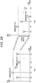
- the information compression unit 311-1 performs grouping on the basis of the opening direction, and performs compression processing on each group. Note that the information compression unit 311-1 recognizes in advance how pixels having different opening directions are arranged in the image capturing unit 121.
- the information compression unit 311-1 performs grouping for each opening direction and performs the first operation or the second operation described above on each group.
- (b) of Fig. 20 illustrates a case where the first operation is performed on each pixel group for each opening direction to generate the compressed information. Note that (b) of Fig. 20 shows the compressed information of the pixel PXFA group, the pixel PXFB group,..., the pixel PXFI group in order from the top.
- Fig. 24 is a diagram showing another example of the second embodiment of the information compression unit.
- (a) of Fig. 24 illustrates the pixel output information before compression.
- the calculation parameter setting unit 3113 sets a power of 2 greater than a ratio of the maximum value of pixel output information before compression to the maximum value of the target bit width as the calculation parameter DPb to be used for dividing the pixel output SDn.
- the linear calculation unit 3114 sets the pixel output information as the compressed information of the target bit width by dividing the pixel output information by the calculation parameter. For example, in a case where the target bit width (TBmax) is 6 bits, since the maximum value of the pixel output information is "240" and the maximum value of the 6-bit range is 63, the calculation parameter DPb is set at "4.”
- the linear calculation unit 3114 computes the calculated value FD0 by dividing the pixel output SD0 at the pixel position G0 by the calculation parameter DPb. Furthermore, the linear calculation unit 3114 computes the calculated value FD1 by dividing the pixel output SD1 at the pixel position G1 by the calculation parameter DPb. In a similar manner below, the linear calculation unit 3114 computes the calculated value FDn by dividing the pixel output SDn at the pixel position Gn by the calculation parameter DPb, and generates the compressed information indicating the calculated values FD0, FD1,... FDn computed in respective pixels. In this way, by dividing the pixel output information by the calculation parameter, the pixel output information after compression (corresponding to the compressed information) shown in (b) of Fig.
- the calculation parameter setting unit 3113 may set the calculation parameter DPa for narrowing a range of a value the pixel output can take on the basis of the amount of light during image capturing, exposure control value, and the like, and the calculation parameter DPb for reducing the bit width to be assigned to the pixel output.
- the calculation parameter setting unit 3113 sets the calculation parameter DPa such that, for example, in a reference exposure setting, the pixel output falls within a range of value the pixel output can take.
- the maximum value of the image output within the range of value the pixel output can take is set as the target bit width.
- the calculation parameter DPb with which the pixel output is set as the target bit width according to the time of exposure to light and gain is set. For example, in a case where the reference exposure setting is that the shutter speed is "(1/128) seconds" and the gain is "one time”, in a case where the gain is set at "double", the calculation parameter DPb is set at the division value "2.”
- the calculation parameter DPb is set at the division value "4.”
- the compressed information may include the calculation parameter.
- the calculation parameter may be included in management data provided in association with the compressed information in order to manage the compressed information and the like.
- the compressed information includes calculation information indicating what linear calculation is performed by the linear calculation unit 3114 to reduce the word length. Note that the calculation parameter does not need to be included in the compressed information if the calculation parameter can be set at the time of information expansion.
- the information expansion unit 321 performs calculation opposite to the calculation of the linear calculation unit 3114 by using the pixel output information and the calculation parameter, thereby generating the pixel output information before the compression processing.
- Fig. 26 is a diagram illustrating the configuration of the third embodiment of an information compression unit.
- an information compression unit 311-3 controls an image capturing unit 121 (221) such that the pixel output information output from the image capturing unit 121 (221) becomes information within a predetermined word length range.
- the information compression unit 311-3 includes, for example, a word length discrimination unit 3115 and an image capturing control unit 3116.
- the word length discrimination unit 3115 discriminates the word length on the basis of the pixel output information output from the image capturing unit 121 (221).
- the word length discrimination unit 3115 may, for example, discriminate the maximum pixel value from the pixel output information of the first frame and discriminate the word length of the maximum pixel value. Since the difference between the detected values is small as described above, the word length discrimination unit 3115 may discriminate the word length for the pixel output information indicating the entire image on the basis of the pixel output of the first pixel output unit.
- the word length discrimination unit 3115 outputs a word length discrimination result to the image capturing control unit 3116.
- the image capturing control unit 3116 On the basis of the word length discrimination result, the image capturing control unit 3116 generates control information for performing exposure control such that the pixel output that is output from the image capturing unit 121 (221) falls within the desired word length, and outputs the control information to the image capturing unit 121 (221).
- the image capturing unit 121 (221) adjusts, for example, the period of exposure to light, the gain, and the like when the image capturing unit 121 (221) generates the pixel output information, and outputs the compressed information, which is the pixel output information within the desired word length.
- the image capturing control unit 3116 generates the control information such that the amount of change in the pixel value in the pixel output information output from the image capturing unit 121 (221) falls within the desired word length, and outputs the control information to the image capturing unit 121 (221).
- the image capturing unit 121 (221) can generate the compressed information in which the amount of change in the pixel value is within the desired word length range.
- the information expansion unit 321 expands the word length of the pixel output information on the basis of the control information to generate the pixel output information before the compression processing.
- the color component image conversion unit 3221 performs reconstruction calculation using red component pixel output information SDr and red component coefficient stored in the coefficient storage unit 323, and computes a pixel value GPr at each pixel position on the image capturing plane IP to generate a red component pixel signal GDr. Furthermore, the color component image conversion unit 3221 performs reconstruction calculation using green component pixel output information SDgr and SDgb and green component coefficient stored in the coefficient storage unit 323, and computes a pixel value GPg at each pixel position on the image capturing plane IP to generate a green component pixel signal GDg.
- the coupling unit 3222 generates a color image signal of three primary colors GDrgb by using the red component pixel signal GDr, the green component pixel signal GDg, and the blue component pixel signal GDb.
- the other configuration of the information processing system shows a case where, in a case where the information compression unit reduces the word length of the pixel output information, image conversion is performed using the pixel output information with reduced word length, and word length reconstruction processing is performed on the image obtained by the image conversion.
- the image capturing unit 121 (221) generates the pixel output information of the pixel value according to the incident angle directivity.
- the information compression unit 311-2 reduces the word length of the pixel output information output from the image capturing unit 121 (221) to perform amount of data compression processing as described above, and outputs the compressed information to an external device by understanding the recording unit 312 or a transmission path.
- the word length reconstruction unit 324 performs word length reconstruction processing corresponding to processing when generating the compressed information from the pixel output information.
- the word length reconstruction unit 324 performs processing of reconstructing the image signal affected by word length reduction to an image signal before compression that is not affected by word length reduction on the basis of the calculation parameter or the control information. For example, in a case where the compressed information is generated by the difference using the calculation parameter, the word length reconstruction unit 324 performs processing of adding the calculation parameter to the image signal output from the image conversion unit 322. Furthermore, in a case where the compressed information is generated by division using the calculation parameter, the word length reconstruction unit 324 performs processing of multiplying the image signal output from the image conversion unit 322 by the calculation parameter.
- the word length reconstruction unit 324 increases the gain by the amount of reduction in the image signal output from the image conversion unit 322.
- the word length reconstruction unit 324 performs such word length reconstruction processing, and reconstructs the image signal of the captured image in which the object captured by the image capturing unit 121 (221) has desired luminous intensity, and outputs the image signal after the word length reconstruction to a display unit or an external device.
- the image conversion unit 322 and the word length reconstruction unit 324 are only required to perform processing for each color component, and to generate the image signal of the captured color image by using the pixel signal of each color component generated by the word length reconstruction unit 324.
- Fig. 31 illustrates the configuration of the image capturing device, and corresponds to the case where the information processing system 300 is applied.
- the image capturing device 50 includes the image capturing unit 121 (221), the information compression unit 311, a recording reproduction unit 315, the information expansion unit 321, the image conversion unit 322, the coefficient storage unit 323, a camera signal processing unit 501, a display unit 502, an output unit 503, a user interface (I/F) unit 504, and a control unit 505.
- the image capturing unit 121 (221) generates the pixel output information according to the incident angle directivity, and outputs the generated pixel output information to the information compression unit 311 and the output unit 503. Furthermore, the image capturing unit 121 (221) performs the image capturing operation and exposure control on the basis of a control signal from the control unit 505.
- the information compression unit 311 performs amount of data compression processing on the pixel output information output from the image capturing unit 121 (221), and generates the compressed information.
- the information compression unit 311 outputs the generated compressed information to the recording reproduction unit 315 and the output unit 503.
- the information expansion unit 321 performs expansion processing on the compressed information supplied from the recording reproduction unit 315, generates the pixel output information before compression processing, and outputs the generated pixel output information to the image conversion unit 322.
- the image conversion unit 322 performs reconstruction calculation using the pixel output information supplied from the image capturing unit 121 (221) or the information expansion unit 321 and the coefficient set group stored in the coefficient storage unit 323, generates the pixel signal according to the image at the corresponding pixel position in the object optical image in each pixel, and outputs the pixel signal to the camera signal processing unit 501.
- the camera signal processing unit 501 In a case where a color sensor including pixels of respective color components is used as the image capturing unit 121 (221), the camera signal processing unit 501 generates the image signal of each color component. Furthermore, the camera signal processing unit 501 performs gamma correction, white balance adjustment, and the like. The camera signal processing unit 501 outputs the processed image signal to the recording reproduction unit 315, the display unit 502, and the output unit 503.
- the display unit 502 includes a liquid crystal display element, an organic EL display element, and the like. On the basis of the image signal output from the camera signal processing unit 501, the display unit 502 displays the image indicating the object captured by the image capturing unit 121 (221). Furthermore, the display unit 502 may perform menu display of the image capturing device 50, or display indicating a setting state or an operation state.
- the output unit 503 selects either one of the pixel output information generated by the image capturing unit 121 (221), the compressed information generated by the information compression unit 311, the image signal processed by the camera signal processing unit 501, and the compressed information or image signal read from the recording medium by the recording reproduction unit 315.
- the output unit 503 outputs the selected information or signal to the outside.
- the output unit 503 may output the image signal to the outside after compressing the image signal in a predetermined compression format, for example, the joint photographic experts group (JPEG), graphics interchange format (GIF), and the like.
- JPEG joint photographic experts group
- GIF graphics interchange format
- the user interface (I/F) unit 504 includes operation buttons, operation switches, and the like, generates an operation signal according to a user operation, and outputs the operation signal to the control unit 505.
- the control unit 505 controls each unit on the basis of the operation signal from the user interface unit 504 such that the operation of the image capturing device 50 is an operation according to the user operation. For example, the control unit 505 controls each unit such that the image conversion unit 322 uses the coefficient set group corresponding to the object distance set by the user from the coefficient set group stored in the coefficient storage unit 323, and an image formed at the object distance is displayed on the display unit 502. Furthermore, by adjusting the object distance such that contrast of the desired object in the image signal generated by the image conversion unit 322 is maximized, a function of so-called autofocus can be implemented.
- control unit 505 may be provided with the function of the image capturing control unit 3116 to perform exposure control of the image capturing unit 121 (221) from the control unit 505.
- the program can be recorded in advance in a hard disk, a solid state drive (SSD), or a read only memory (ROM) serving as a recording medium.
- the program can be temporarily or permanently stored (recorded) in a removable recording medium including a flexible disk, a compact disc read only memory (CD-ROM), a magneto optical (MO) disk, a digital versatile disc (DVD), a Blu-ray disc (BD) (registered trademark), a magnetic disk, a semiconductor memory card, and the like.
- a removable recording medium can be provided as so-called package software.
- the information processing device of the present technology can also have the following configurations.
- an information compression unit performs compression processing to reduce an amount of data of pixel output information including a plurality of pixel outputs that is output from an image capturing element including a plurality of pixel output units configured to receive object light that enters without passing through any of an image capturing lens and a pinhole, and among the plurality of pixel output units, the pixel outputs of at least two of the pixel output units have incident angle directivity modulated into different incident angle directivity according to an incident angle of the object light. Therefore, an amount of data in a case where an image capturing element of image capturing lens free is used can be reduced. Therefore, it is possible to improve the degree of freedom in designing the configuration for image capturing and to reduce the amount of data during image capturing.
Landscapes
- Engineering & Computer Science (AREA)
- Multimedia (AREA)
- Signal Processing (AREA)
- Computing Systems (AREA)
- Theoretical Computer Science (AREA)
- Transforming Light Signals Into Electric Signals (AREA)
- Solid State Image Pick-Up Elements (AREA)
- Studio Devices (AREA)
Applications Claiming Priority (2)
| Application Number | Priority Date | Filing Date | Title |
|---|---|---|---|
| JP2017202354 | 2017-10-19 | ||
| PCT/JP2018/038920 WO2019078319A1 (ja) | 2017-10-19 | 2018-10-19 | 情報処理装置と情報処理方法および撮像装置とプログラム |
Publications (3)
| Publication Number | Publication Date |
|---|---|
| EP3700185A4 EP3700185A4 (de) | 2020-08-26 |
| EP3700185A1 true EP3700185A1 (de) | 2020-08-26 |
| EP3700185B1 EP3700185B1 (de) | 2021-12-01 |
Family
ID=66173292
Family Applications (1)
| Application Number | Title | Priority Date | Filing Date |
|---|---|---|---|
| EP18867663.9A Not-in-force EP3700185B1 (de) | 2017-10-19 | 2018-10-19 | Informationsverarbeitungsvorrichtung, informationsverarbeitungsverfahren, bilderzeugendes verfahren, und programm |
Country Status (5)
| Country | Link |
|---|---|
| US (1) | US11631713B2 (de) |
| EP (1) | EP3700185B1 (de) |
| JP (1) | JP7180609B2 (de) |
| CN (1) | CN111201775B (de) |
| WO (1) | WO2019078319A1 (de) |
Cited By (1)
| Publication number | Priority date | Publication date | Assignee | Title |
|---|---|---|---|---|
| EP3780576A4 (de) * | 2018-03-29 | 2021-04-21 | Sony Corporation | Informationsverarbeitungsvorrichtung, informationsverarbeitungsverfahren, programm und informationsverarbeitungssystem |
Families Citing this family (3)
| Publication number | Priority date | Publication date | Assignee | Title |
|---|---|---|---|---|
| US11368609B2 (en) * | 2017-10-19 | 2022-06-21 | Sony Corporation | Electronic apparatus |
| KR20230020857A (ko) * | 2021-08-04 | 2023-02-13 | 에스케이하이닉스 주식회사 | 이미지 센싱 장치 |
| GB202207253D0 (en) * | 2022-05-18 | 2022-06-29 | Ams Int Ag | Optoelectronic module |
Family Cites Families (7)
| Publication number | Priority date | Publication date | Assignee | Title |
|---|---|---|---|---|
| JP4508132B2 (ja) | 2006-02-27 | 2010-07-21 | ソニー株式会社 | 撮像装置、撮像回路、および撮像方法 |
| JP2009038740A (ja) * | 2007-08-03 | 2009-02-19 | Panasonic Corp | 画像符号化装置 |
| KR101375830B1 (ko) | 2009-11-16 | 2014-03-17 | 캐논 가부시끼가이샤 | 촬상장치 및 그 제어방법 |
| US9971078B2 (en) | 2013-03-05 | 2018-05-15 | Rambus Inc. | Phase gratings with odd symmetry for high-resolution lensless optical sensing |
| US9761730B2 (en) | 2014-10-29 | 2017-09-12 | Semiconductor Energy Laboratory Co., Ltd. | Imaging device and electronic device |
| WO2016123529A1 (en) | 2015-01-29 | 2016-08-04 | William Marsh Rice University | Lensless imaging system using an image sensor with one or more attenuating layers |
| EP3358618B1 (de) | 2015-09-29 | 2021-08-11 | Dai Nippon Printing Co., Ltd. | Bildgebungsmodul und bildgebungsvorrichtung |
-
2018
- 2018-10-19 US US16/754,592 patent/US11631713B2/en active Active
- 2018-10-19 EP EP18867663.9A patent/EP3700185B1/de not_active Not-in-force
- 2018-10-19 CN CN201880066092.XA patent/CN111201775B/zh active Active
- 2018-10-19 WO PCT/JP2018/038920 patent/WO2019078319A1/ja not_active Ceased
- 2018-10-19 JP JP2019549350A patent/JP7180609B2/ja active Active
Cited By (2)
| Publication number | Priority date | Publication date | Assignee | Title |
|---|---|---|---|---|
| EP3780576A4 (de) * | 2018-03-29 | 2021-04-21 | Sony Corporation | Informationsverarbeitungsvorrichtung, informationsverarbeitungsverfahren, programm und informationsverarbeitungssystem |
| US11470247B2 (en) | 2018-03-29 | 2022-10-11 | Sony Corporation | Information processing device, information processing method, program, and information processing system |
Also Published As
| Publication number | Publication date |
|---|---|
| US20200295073A1 (en) | 2020-09-17 |
| CN111201775A (zh) | 2020-05-26 |
| US11631713B2 (en) | 2023-04-18 |
| CN111201775B (zh) | 2022-01-18 |
| WO2019078319A1 (ja) | 2019-04-25 |
| EP3700185A4 (de) | 2020-08-26 |
| JP7180609B2 (ja) | 2022-11-30 |
| EP3700185B1 (de) | 2021-12-01 |
| JPWO2019078319A1 (ja) | 2020-11-19 |
Similar Documents
| Publication | Publication Date | Title |
|---|---|---|
| JP6179827B2 (ja) | フォーカス信号を生成する方法 | |
| JP5830348B2 (ja) | 撮像装置 | |
| US9807332B2 (en) | Image capturing apparatus and method for controlling the same | |
| EP3700185B1 (de) | Informationsverarbeitungsvorrichtung, informationsverarbeitungsverfahren, bilderzeugendes verfahren, und programm | |
| CN101778222B (zh) | 图像处理装置 | |
| JP6555863B2 (ja) | 撮像装置及び撮像装置の制御方法 | |
| US12114081B2 (en) | Systems and methods for creating a full-color image in low light | |
| CN104125394B (zh) | 摄像装置及其控制方法 | |
| US20170302867A1 (en) | Image processing apparatus, image processing method, and computer-readable recording medium | |
| US10158811B2 (en) | Image processing apparatus, image processing method, and computer-readable recording medium | |
| US9813687B1 (en) | Image-capturing device, image-processing device, image-processing method, and image-processing program | |
| US8279308B1 (en) | Optimized log encoding of image data | |
| JP5920608B2 (ja) | 画像の鮮明度を評価する撮像システムおよび方法 | |
| US11223787B2 (en) | Information processing apparatus, information processing method, and imaging apparatus | |
| CN104919352A (zh) | 摄像装置和图像校正方法以及图像处理装置和图像处理方法 | |
| JP6211137B2 (ja) | 画像処理装置、撮像装置、及び画像処理方法 | |
| JP2015035782A (ja) | 画像処理装置、撮像装置、顕微鏡システム、画像処理方法及び画像処理プログラム | |
| WO2019078333A1 (ja) | 撮像装置、露出制御方法、プログラム、及び、撮像素子 | |
| US11252361B2 (en) | Imaging element, imaging device, and information processing method with image restoration pixels and unidirectional pixel | |
| JPWO2019188396A1 (ja) | 撮像装置および方法、画像処理装置および方法、並びに、撮像素子 | |
| US20170094152A1 (en) | Image processing apparatus, image processing method, and image capture apparatus and control method thereof | |
| AU2011340207A1 (en) | Auto-focus image system | |
| JP2014504375A5 (de) | ||
| US10341556B2 (en) | Image capturing apparatus and control method therefor | |
| JP2016072893A (ja) | 画像処理装置、画像処理方法およびプログラム、並びに撮像装置 |
Legal Events
| Date | Code | Title | Description |
|---|---|---|---|
| STAA | Information on the status of an ep patent application or granted ep patent |
Free format text: STATUS: THE INTERNATIONAL PUBLICATION HAS BEEN MADE |
|
| PUAI | Public reference made under article 153(3) epc to a published international application that has entered the european phase |
Free format text: ORIGINAL CODE: 0009012 |
|
| STAA | Information on the status of an ep patent application or granted ep patent |
Free format text: STATUS: REQUEST FOR EXAMINATION WAS MADE |
|
| 17P | Request for examination filed |
Effective date: 20200329 |
|
| A4 | Supplementary search report drawn up and despatched |
Effective date: 20200709 |
|
| AK | Designated contracting states |
Kind code of ref document: A1 Designated state(s): AL AT BE BG CH CY CZ DE DK EE ES FI FR GB GR HR HU IE IS IT LI LT LU LV MC MK MT NL NO PL PT RO RS SE SI SK SM TR |
|
| AX | Request for extension of the european patent |
Extension state: BA ME |
|
| DAV | Request for validation of the european patent (deleted) | ||
| DAX | Request for extension of the european patent (deleted) | ||
| GRAP | Despatch of communication of intention to grant a patent |
Free format text: ORIGINAL CODE: EPIDOSNIGR1 |
|
| STAA | Information on the status of an ep patent application or granted ep patent |
Free format text: STATUS: GRANT OF PATENT IS INTENDED |
|
| RAP3 | Party data changed (applicant data changed or rights of an application transferred) |
Owner name: SONY CORPORATION |
|
| INTG | Intention to grant announced |
Effective date: 20210621 |
|
| RAP3 | Party data changed (applicant data changed or rights of an application transferred) |
Owner name: SONY GROUP CORPORATION |
|
| GRAS | Grant fee paid |
Free format text: ORIGINAL CODE: EPIDOSNIGR3 |
|
| GRAA | (expected) grant |
Free format text: ORIGINAL CODE: 0009210 |
|
| STAA | Information on the status of an ep patent application or granted ep patent |
Free format text: STATUS: THE PATENT HAS BEEN GRANTED |
|
| AK | Designated contracting states |
Kind code of ref document: B1 Designated state(s): AL AT BE BG CH CY CZ DE DK EE ES FI FR GB GR HR HU IE IS IT LI LT LU LV MC MK MT NL NO PL PT RO RS SE SI SK SM TR |
|
| REG | Reference to a national code |
Ref country code: GB Ref legal event code: FG4D |
|
| REG | Reference to a national code |
Ref country code: AT Ref legal event code: REF Ref document number: 1452889 Country of ref document: AT Kind code of ref document: T Effective date: 20211215 Ref country code: CH Ref legal event code: EP |
|
| REG | Reference to a national code |
Ref country code: IE Ref legal event code: FG4D |
|
| REG | Reference to a national code |
Ref country code: DE Ref legal event code: R096 Ref document number: 602018027718 Country of ref document: DE |
|
| REG | Reference to a national code |
Ref country code: LT Ref legal event code: MG9D |
|
| REG | Reference to a national code |
Ref country code: NL Ref legal event code: MP Effective date: 20211201 |
|
| REG | Reference to a national code |
Ref country code: AT Ref legal event code: MK05 Ref document number: 1452889 Country of ref document: AT Kind code of ref document: T Effective date: 20211201 |
|
| PG25 | Lapsed in a contracting state [announced via postgrant information from national office to epo] |
Ref country code: RS Free format text: LAPSE BECAUSE OF FAILURE TO SUBMIT A TRANSLATION OF THE DESCRIPTION OR TO PAY THE FEE WITHIN THE PRESCRIBED TIME-LIMIT Effective date: 20211201 Ref country code: LT Free format text: LAPSE BECAUSE OF FAILURE TO SUBMIT A TRANSLATION OF THE DESCRIPTION OR TO PAY THE FEE WITHIN THE PRESCRIBED TIME-LIMIT Effective date: 20211201 Ref country code: FI Free format text: LAPSE BECAUSE OF FAILURE TO SUBMIT A TRANSLATION OF THE DESCRIPTION OR TO PAY THE FEE WITHIN THE PRESCRIBED TIME-LIMIT Effective date: 20211201 Ref country code: BG Free format text: LAPSE BECAUSE OF FAILURE TO SUBMIT A TRANSLATION OF THE DESCRIPTION OR TO PAY THE FEE WITHIN THE PRESCRIBED TIME-LIMIT Effective date: 20220301 Ref country code: AT Free format text: LAPSE BECAUSE OF FAILURE TO SUBMIT A TRANSLATION OF THE DESCRIPTION OR TO PAY THE FEE WITHIN THE PRESCRIBED TIME-LIMIT Effective date: 20211201 |
|
| PG25 | Lapsed in a contracting state [announced via postgrant information from national office to epo] |
Ref country code: SE Free format text: LAPSE BECAUSE OF FAILURE TO SUBMIT A TRANSLATION OF THE DESCRIPTION OR TO PAY THE FEE WITHIN THE PRESCRIBED TIME-LIMIT Effective date: 20211201 Ref country code: PL Free format text: LAPSE BECAUSE OF FAILURE TO SUBMIT A TRANSLATION OF THE DESCRIPTION OR TO PAY THE FEE WITHIN THE PRESCRIBED TIME-LIMIT Effective date: 20211201 Ref country code: NO Free format text: LAPSE BECAUSE OF FAILURE TO SUBMIT A TRANSLATION OF THE DESCRIPTION OR TO PAY THE FEE WITHIN THE PRESCRIBED TIME-LIMIT Effective date: 20220301 Ref country code: LV Free format text: LAPSE BECAUSE OF FAILURE TO SUBMIT A TRANSLATION OF THE DESCRIPTION OR TO PAY THE FEE WITHIN THE PRESCRIBED TIME-LIMIT Effective date: 20211201 Ref country code: HR Free format text: LAPSE BECAUSE OF FAILURE TO SUBMIT A TRANSLATION OF THE DESCRIPTION OR TO PAY THE FEE WITHIN THE PRESCRIBED TIME-LIMIT Effective date: 20211201 Ref country code: GR Free format text: LAPSE BECAUSE OF FAILURE TO SUBMIT A TRANSLATION OF THE DESCRIPTION OR TO PAY THE FEE WITHIN THE PRESCRIBED TIME-LIMIT Effective date: 20220302 |
|
| PG25 | Lapsed in a contracting state [announced via postgrant information from national office to epo] |
Ref country code: NL Free format text: LAPSE BECAUSE OF FAILURE TO SUBMIT A TRANSLATION OF THE DESCRIPTION OR TO PAY THE FEE WITHIN THE PRESCRIBED TIME-LIMIT Effective date: 20211201 |
|
| PG25 | Lapsed in a contracting state [announced via postgrant information from national office to epo] |
Ref country code: SM Free format text: LAPSE BECAUSE OF FAILURE TO SUBMIT A TRANSLATION OF THE DESCRIPTION OR TO PAY THE FEE WITHIN THE PRESCRIBED TIME-LIMIT Effective date: 20211201 Ref country code: SK Free format text: LAPSE BECAUSE OF FAILURE TO SUBMIT A TRANSLATION OF THE DESCRIPTION OR TO PAY THE FEE WITHIN THE PRESCRIBED TIME-LIMIT Effective date: 20211201 Ref country code: RO Free format text: LAPSE BECAUSE OF FAILURE TO SUBMIT A TRANSLATION OF THE DESCRIPTION OR TO PAY THE FEE WITHIN THE PRESCRIBED TIME-LIMIT Effective date: 20211201 Ref country code: PT Free format text: LAPSE BECAUSE OF FAILURE TO SUBMIT A TRANSLATION OF THE DESCRIPTION OR TO PAY THE FEE WITHIN THE PRESCRIBED TIME-LIMIT Effective date: 20220401 Ref country code: ES Free format text: LAPSE BECAUSE OF FAILURE TO SUBMIT A TRANSLATION OF THE DESCRIPTION OR TO PAY THE FEE WITHIN THE PRESCRIBED TIME-LIMIT Effective date: 20211201 Ref country code: EE Free format text: LAPSE BECAUSE OF FAILURE TO SUBMIT A TRANSLATION OF THE DESCRIPTION OR TO PAY THE FEE WITHIN THE PRESCRIBED TIME-LIMIT Effective date: 20211201 Ref country code: CZ Free format text: LAPSE BECAUSE OF FAILURE TO SUBMIT A TRANSLATION OF THE DESCRIPTION OR TO PAY THE FEE WITHIN THE PRESCRIBED TIME-LIMIT Effective date: 20211201 |
|
| REG | Reference to a national code |
Ref country code: DE Ref legal event code: R097 Ref document number: 602018027718 Country of ref document: DE |
|
| PG25 | Lapsed in a contracting state [announced via postgrant information from national office to epo] |
Ref country code: IS Free format text: LAPSE BECAUSE OF FAILURE TO SUBMIT A TRANSLATION OF THE DESCRIPTION OR TO PAY THE FEE WITHIN THE PRESCRIBED TIME-LIMIT Effective date: 20220401 |
|
| PLBE | No opposition filed within time limit |
Free format text: ORIGINAL CODE: 0009261 |
|
| STAA | Information on the status of an ep patent application or granted ep patent |
Free format text: STATUS: NO OPPOSITION FILED WITHIN TIME LIMIT |
|
| PG25 | Lapsed in a contracting state [announced via postgrant information from national office to epo] |
Ref country code: DK Free format text: LAPSE BECAUSE OF FAILURE TO SUBMIT A TRANSLATION OF THE DESCRIPTION OR TO PAY THE FEE WITHIN THE PRESCRIBED TIME-LIMIT Effective date: 20211201 Ref country code: AL Free format text: LAPSE BECAUSE OF FAILURE TO SUBMIT A TRANSLATION OF THE DESCRIPTION OR TO PAY THE FEE WITHIN THE PRESCRIBED TIME-LIMIT Effective date: 20211201 |
|
| 26N | No opposition filed |
Effective date: 20220902 |
|
| REG | Reference to a national code |
Ref country code: DE Ref legal event code: R079 Ref document number: 602018027718 Country of ref document: DE Free format text: PREVIOUS MAIN CLASS: H04N0005232000 Ipc: H04N0023600000 |
|
| PG25 | Lapsed in a contracting state [announced via postgrant information from national office to epo] |
Ref country code: SI Free format text: LAPSE BECAUSE OF FAILURE TO SUBMIT A TRANSLATION OF THE DESCRIPTION OR TO PAY THE FEE WITHIN THE PRESCRIBED TIME-LIMIT Effective date: 20211201 |
|
| PG25 | Lapsed in a contracting state [announced via postgrant information from national office to epo] |
Ref country code: MC Free format text: LAPSE BECAUSE OF FAILURE TO SUBMIT A TRANSLATION OF THE DESCRIPTION OR TO PAY THE FEE WITHIN THE PRESCRIBED TIME-LIMIT Effective date: 20211201 Ref country code: IT Free format text: LAPSE BECAUSE OF FAILURE TO SUBMIT A TRANSLATION OF THE DESCRIPTION OR TO PAY THE FEE WITHIN THE PRESCRIBED TIME-LIMIT Effective date: 20211201 |
|
| REG | Reference to a national code |
Ref country code: CH Ref legal event code: PL |
|
| REG | Reference to a national code |
Ref country code: BE Ref legal event code: MM Effective date: 20221031 |
|
| GBPC | Gb: european patent ceased through non-payment of renewal fee |
Effective date: 20221019 |
|
| PG25 | Lapsed in a contracting state [announced via postgrant information from national office to epo] |
Ref country code: LU Free format text: LAPSE BECAUSE OF NON-PAYMENT OF DUE FEES Effective date: 20221019 |
|
| P01 | Opt-out of the competence of the unified patent court (upc) registered |
Effective date: 20230528 |
|
| PG25 | Lapsed in a contracting state [announced via postgrant information from national office to epo] |
Ref country code: LI Free format text: LAPSE BECAUSE OF NON-PAYMENT OF DUE FEES Effective date: 20221031 Ref country code: FR Free format text: LAPSE BECAUSE OF NON-PAYMENT OF DUE FEES Effective date: 20221031 Ref country code: CH Free format text: LAPSE BECAUSE OF NON-PAYMENT OF DUE FEES Effective date: 20221031 |
|
| PG25 | Lapsed in a contracting state [announced via postgrant information from national office to epo] |
Ref country code: BE Free format text: LAPSE BECAUSE OF NON-PAYMENT OF DUE FEES Effective date: 20221031 |
|
| PG25 | Lapsed in a contracting state [announced via postgrant information from national office to epo] |
Ref country code: IE Free format text: LAPSE BECAUSE OF NON-PAYMENT OF DUE FEES Effective date: 20221019 Ref country code: GB Free format text: LAPSE BECAUSE OF NON-PAYMENT OF DUE FEES Effective date: 20221019 |
|
| PGFP | Annual fee paid to national office [announced via postgrant information from national office to epo] |
Ref country code: DE Payment date: 20230920 Year of fee payment: 6 |
|
| PG25 | Lapsed in a contracting state [announced via postgrant information from national office to epo] |
Ref country code: CY Free format text: LAPSE BECAUSE OF FAILURE TO SUBMIT A TRANSLATION OF THE DESCRIPTION OR TO PAY THE FEE WITHIN THE PRESCRIBED TIME-LIMIT Effective date: 20211201 |
|
| PG25 | Lapsed in a contracting state [announced via postgrant information from national office to epo] |
Ref country code: MK Free format text: LAPSE BECAUSE OF FAILURE TO SUBMIT A TRANSLATION OF THE DESCRIPTION OR TO PAY THE FEE WITHIN THE PRESCRIBED TIME-LIMIT Effective date: 20211201 Ref country code: HU Free format text: LAPSE BECAUSE OF FAILURE TO SUBMIT A TRANSLATION OF THE DESCRIPTION OR TO PAY THE FEE WITHIN THE PRESCRIBED TIME-LIMIT; INVALID AB INITIO Effective date: 20181019 |
|
| PG25 | Lapsed in a contracting state [announced via postgrant information from national office to epo] |
Ref country code: TR Free format text: LAPSE BECAUSE OF FAILURE TO SUBMIT A TRANSLATION OF THE DESCRIPTION OR TO PAY THE FEE WITHIN THE PRESCRIBED TIME-LIMIT Effective date: 20211201 |
|
| PG25 | Lapsed in a contracting state [announced via postgrant information from national office to epo] |
Ref country code: MT Free format text: LAPSE BECAUSE OF FAILURE TO SUBMIT A TRANSLATION OF THE DESCRIPTION OR TO PAY THE FEE WITHIN THE PRESCRIBED TIME-LIMIT Effective date: 20211201 |
|
| REG | Reference to a national code |
Ref country code: DE Ref legal event code: R119 Ref document number: 602018027718 Country of ref document: DE |
|
| PG25 | Lapsed in a contracting state [announced via postgrant information from national office to epo] |
Ref country code: DE Free format text: LAPSE BECAUSE OF NON-PAYMENT OF DUE FEES Effective date: 20250501 |