EP3702130B1 - Stereolithografiegerät und ein verfahren zum einstellen eines stereolithografiegerätes - Google Patents
Stereolithografiegerät und ein verfahren zum einstellen eines stereolithografiegerätes Download PDFInfo
- Publication number
- EP3702130B1 EP3702130B1 EP19159596.6A EP19159596A EP3702130B1 EP 3702130 B1 EP3702130 B1 EP 3702130B1 EP 19159596 A EP19159596 A EP 19159596A EP 3702130 B1 EP3702130 B1 EP 3702130B1
- Authority
- EP
- European Patent Office
- Prior art keywords
- light
- sensor
- stereolithography apparatus
- onto
- light source
- Prior art date
- Legal status (The legal status is an assumption and is not a legal conclusion. Google has not performed a legal analysis and makes no representation as to the accuracy of the status listed.)
- Active
Links
Images

Classifications
-
- B—PERFORMING OPERATIONS; TRANSPORTING
- B29—WORKING OF PLASTICS; WORKING OF SUBSTANCES IN A PLASTIC STATE IN GENERAL
- B29C—SHAPING OR JOINING OF PLASTICS; SHAPING OF MATERIAL IN A PLASTIC STATE, NOT OTHERWISE PROVIDED FOR; AFTER-TREATMENT OF THE SHAPED PRODUCTS, e.g. REPAIRING
- B29C64/00—Additive manufacturing, i.e. manufacturing of three-dimensional [3D] objects by additive deposition, additive agglomeration or additive layering, e.g. by 3D printing, stereolithography or selective laser sintering
- B29C64/10—Processes of additive manufacturing
- B29C64/106—Processes of additive manufacturing using only liquids or viscous materials, e.g. depositing a continuous bead of viscous material
- B29C64/124—Processes of additive manufacturing using only liquids or viscous materials, e.g. depositing a continuous bead of viscous material using layers of liquid which are selectively solidified
-
- B—PERFORMING OPERATIONS; TRANSPORTING
- B29—WORKING OF PLASTICS; WORKING OF SUBSTANCES IN A PLASTIC STATE IN GENERAL
- B29C—SHAPING OR JOINING OF PLASTICS; SHAPING OF MATERIAL IN A PLASTIC STATE, NOT OTHERWISE PROVIDED FOR; AFTER-TREATMENT OF THE SHAPED PRODUCTS, e.g. REPAIRING
- B29C64/00—Additive manufacturing, i.e. manufacturing of three-dimensional [3D] objects by additive deposition, additive agglomeration or additive layering, e.g. by 3D printing, stereolithography or selective laser sintering
- B29C64/10—Processes of additive manufacturing
- B29C64/106—Processes of additive manufacturing using only liquids or viscous materials, e.g. depositing a continuous bead of viscous material
- B29C64/124—Processes of additive manufacturing using only liquids or viscous materials, e.g. depositing a continuous bead of viscous material using layers of liquid which are selectively solidified
- B29C64/129—Processes of additive manufacturing using only liquids or viscous materials, e.g. depositing a continuous bead of viscous material using layers of liquid which are selectively solidified characterised by the energy source therefor, e.g. by global irradiation combined with a mask
-
- B—PERFORMING OPERATIONS; TRANSPORTING
- B29—WORKING OF PLASTICS; WORKING OF SUBSTANCES IN A PLASTIC STATE IN GENERAL
- B29C—SHAPING OR JOINING OF PLASTICS; SHAPING OF MATERIAL IN A PLASTIC STATE, NOT OTHERWISE PROVIDED FOR; AFTER-TREATMENT OF THE SHAPED PRODUCTS, e.g. REPAIRING
- B29C64/00—Additive manufacturing, i.e. manufacturing of three-dimensional [3D] objects by additive deposition, additive agglomeration or additive layering, e.g. by 3D printing, stereolithography or selective laser sintering
- B29C64/20—Apparatus for additive manufacturing; Details thereof or accessories therefor
- B29C64/264—Arrangements for irradiation
-
- B—PERFORMING OPERATIONS; TRANSPORTING
- B29—WORKING OF PLASTICS; WORKING OF SUBSTANCES IN A PLASTIC STATE IN GENERAL
- B29C—SHAPING OR JOINING OF PLASTICS; SHAPING OF MATERIAL IN A PLASTIC STATE, NOT OTHERWISE PROVIDED FOR; AFTER-TREATMENT OF THE SHAPED PRODUCTS, e.g. REPAIRING
- B29C64/00—Additive manufacturing, i.e. manufacturing of three-dimensional [3D] objects by additive deposition, additive agglomeration or additive layering, e.g. by 3D printing, stereolithography or selective laser sintering
- B29C64/30—Auxiliary operations or equipment
- B29C64/386—Data acquisition or data processing for additive manufacturing
- B29C64/393—Data acquisition or data processing for additive manufacturing for controlling or regulating additive manufacturing processes
-
- B—PERFORMING OPERATIONS; TRANSPORTING
- B33—ADDITIVE MANUFACTURING TECHNOLOGY
- B33Y—ADDITIVE MANUFACTURING, i.e. MANUFACTURING OF THREE-DIMENSIONAL [3D] OBJECTS BY ADDITIVE DEPOSITION, ADDITIVE AGGLOMERATION OR ADDITIVE LAYERING, e.g. BY 3D PRINTING, STEREOLITHOGRAPHY OR SELECTIVE LASER SINTERING
- B33Y30/00—Apparatus for additive manufacturing; Details thereof or accessories therefor
-
- B—PERFORMING OPERATIONS; TRANSPORTING
- B33—ADDITIVE MANUFACTURING TECHNOLOGY
- B33Y—ADDITIVE MANUFACTURING, i.e. MANUFACTURING OF THREE-DIMENSIONAL [3D] OBJECTS BY ADDITIVE DEPOSITION, ADDITIVE AGGLOMERATION OR ADDITIVE LAYERING, e.g. BY 3D PRINTING, STEREOLITHOGRAPHY OR SELECTIVE LASER SINTERING
- B33Y50/00—Data acquisition or data processing for additive manufacturing
- B33Y50/02—Data acquisition or data processing for additive manufacturing for controlling or regulating additive manufacturing processes
-
- G—PHYSICS
- G02—OPTICS
- G02B—OPTICAL ELEMENTS, SYSTEMS OR APPARATUS
- G02B26/00—Optical devices or arrangements for the control of light using movable or deformable optical elements
- G02B26/08—Optical devices or arrangements for the control of light using movable or deformable optical elements for controlling the direction of light
- G02B26/0816—Optical devices or arrangements for the control of light using movable or deformable optical elements for controlling the direction of light by means of one or more reflecting elements
- G02B26/0833—Optical devices or arrangements for the control of light using movable or deformable optical elements for controlling the direction of light by means of one or more reflecting elements the reflecting element being a micromechanical device, e.g. a MEMS mirror, DMD
-
- H—ELECTRICITY
- H05—ELECTRIC TECHNIQUES NOT OTHERWISE PROVIDED FOR
- H05B—ELECTRIC HEATING; ELECTRIC LIGHT SOURCES NOT OTHERWISE PROVIDED FOR; CIRCUIT ARRANGEMENTS FOR ELECTRIC LIGHT SOURCES, IN GENERAL
- H05B47/00—Circuit arrangements for operating light sources in general, i.e. where the type of light source is not relevant
- H05B47/10—Controlling the light source
- H05B47/105—Controlling the light source in response to determined parameters
-
- B—PERFORMING OPERATIONS; TRANSPORTING
- B29—WORKING OF PLASTICS; WORKING OF SUBSTANCES IN A PLASTIC STATE IN GENERAL
- B29C—SHAPING OR JOINING OF PLASTICS; SHAPING OF MATERIAL IN A PLASTIC STATE, NOT OTHERWISE PROVIDED FOR; AFTER-TREATMENT OF THE SHAPED PRODUCTS, e.g. REPAIRING
- B29C64/00—Additive manufacturing, i.e. manufacturing of three-dimensional [3D] objects by additive deposition, additive agglomeration or additive layering, e.g. by 3D printing, stereolithography or selective laser sintering
- B29C64/20—Apparatus for additive manufacturing; Details thereof or accessories therefor
- B29C64/264—Arrangements for irradiation
- B29C64/277—Arrangements for irradiation using multiple radiation means, e.g. micromirrors or multiple light-emitting diodes [LED]
-
- B—PERFORMING OPERATIONS; TRANSPORTING
- B29—WORKING OF PLASTICS; WORKING OF SUBSTANCES IN A PLASTIC STATE IN GENERAL
- B29C—SHAPING OR JOINING OF PLASTICS; SHAPING OF MATERIAL IN A PLASTIC STATE, NOT OTHERWISE PROVIDED FOR; AFTER-TREATMENT OF THE SHAPED PRODUCTS, e.g. REPAIRING
- B29C64/00—Additive manufacturing, i.e. manufacturing of three-dimensional [3D] objects by additive deposition, additive agglomeration or additive layering, e.g. by 3D printing, stereolithography or selective laser sintering
- B29C64/20—Apparatus for additive manufacturing; Details thereof or accessories therefor
- B29C64/264—Arrangements for irradiation
- B29C64/277—Arrangements for irradiation using multiple radiation means, e.g. micromirrors or multiple light-emitting diodes [LED]
- B29C64/282—Arrangements for irradiation using multiple radiation means, e.g. micromirrors or multiple light-emitting diodes [LED] of the same type, e.g. using different energy levels
Definitions
- the present invention relates to a stereolithography apparatus and a method for adjusting a stereolithography apparatus.
- Stereolithography is a three-dimensional printing process in which a workpiece is built up step by step from a liquid bath made of a photopolymer, or the workpiece is created in a liquid bath using a construction platform.
- the construction platform is first introduced into the liquid bath and removed from the liquid bath after individual layers have been formed.
- the construction platform is then reinserted into the liquid bath until the desired object is produced.
- a pattern of light is projected onto the photopolymer at each step.
- the photopolymer hardens at the points where the light pattern hits it. In this way, the workpiece can be manufactured layer by layer with the desired shape.
- An ultraviolet light source (eg LED) of the stereolithography device is affected by aging effects over the required service life, so that the light intensity decreases with constant electrical current.
- Other components in the light path such as prisms, lenses, light mixing rods and electronic mirror devices, also show degradation effects due to the high exposure to UV light, which is reflected in a reduced exposure intensity on the construction site manifest.
- the pamphlet EP 18 190 700.7 relates to a method for the layered construction of a shaped body by stereolithographic curing of photopolymerizable material in successive layers by exposure to light using an exposure unit.
- the pamphlet EP 1 894 704 A1 relates to a technique for obtaining improved wall smoothness and feature accuracy in an image projection system, which is obtained from the projected size of the pixels.
- the pamphlet WO 2013/170311 A1 refers to a device for crafting an object.
- the device includes a radiation source, such as a light emitting diode.
- a prism directs the radiation onto a spatial light modulator (SLM), such as a DLP micro-electromechanical system (MEMS).
- SLM spatial light modulator
- MEMS micro-electromechanical system
- the pamphlet EP 3 470 210 A1 (Prior art under Art. 54(3) EPC) relates to a 3D printing device.
- the 3D printing device includes a light source 110 and a digital mirror device. Part of the light hits the first micro-mirrors, which direct this part onto the working liquid in order to harden it and create the 3D printed object.
- the pamphlet U.S. 2018/186066 A1 relates to an apparatus for making a three-dimensional article.
- An alternator 10 is configured to apply a pixel image onto a build plane project.
- a sensor records the intensity for each pixel in the entire build plane.
- the problem has either been ignored or solved with aging compensation, in which the exposure time and/or the current intensity of the light source are adjusted over time using a permanently stored characteristic.
- the stored characteristic does not take into account the individual variation of the components used. Controlling the light intensity via the aging characteristics of the light source and the unpredictable aging behavior of the remaining light path is therefore imprecise.
- the digital mirror device is arranged adjacent to a prism surface. This achieves the technical advantage, for example, that the size of the stereolithography device can be reduced.
- the stereolithography device is designed to project a predetermined light pattern through the digital mirror device onto the sensor. This achieves the technical advantage, for example, that the amount of light can be precisely dosed onto the sensor.
- the stereolithography device comprises a mirror surface for deflecting the light onto the sensor.
- the mirror surface is arranged adjacent to a prismatic screen. This achieves the technical advantage, for example, that the prismatic screen defines a predetermined exit opening and unwanted scattered light is reduced.
- the senor is designed specifically for detecting ultraviolet light. This achieves the technical advantage, for example, that the sensor has a long service life.
- the senor is formed by a photodiode. This achieves the technical advantage, for example, that the sensor is inexpensive and at the same time has few signs of aging.
- control unit includes a controller for controlling the current through the light source, such as a PID controller or PI controller.
- a controller for controlling the current through the light source such as a PID controller or PI controller.
- this object is achieved by a method for adjusting a stereolithography device, with the steps of emitting light for curing a light-curing material using a light source; a determination of an actual value of the light intensity of the emitted light; and adjusting the electrical current through the light source until the actual value of the light intensity reaches a predetermined target value.
- the method achieves the same technical advantages as the stereolithography apparatus of the first aspect, wherein the light from the light source is redirected to the sensor by a digital mirror device which is used to project a pattern of light onto the photocurable material. This also achieves the technical advantage, for example, that the light can be directed onto a decoupling light path as required, and the service life of the sensor is increased.
- a predetermined light pattern is projected onto the sensor by the digital mirror device. This also achieves the technical advantage, for example, that the light impinging on the sensor can be dosed.
- the light is deflected onto the sensor via a mirror surface.
- the sensor can be arranged flexibly at different positions inside the stereolithography device.
- the current is regulated to the desired value by a controller, such as a PID controller.
- control circuit is regulated quickly and efficiently.
- the light is guided through a prism screen.
- the prismatic screen defines a predetermined exit opening and the determination of the actual value is carried out in a comparable manner for different measurements. Exemplary embodiments of the invention are shown in the drawings and are described in more detail below.
- the stereolithography device 100 is used to produce workpieces by means of a three-dimensional printing process (3D printing).
- 3D printing three-dimensional printing process
- the workpiece is in a liquid bath made of a light-curing material, such as a photopolymer, which is built up step by step.
- a specific light pattern 123 is projected onto the light-curing material 121 at each step. Where the pattern of light 123 strikes the light-curable material, it hardens and becomes solid. In this way, the workpiece can be manufactured layer by layer with the desired shape.
- the stereolithography machine 100 includes a light source 101, such as an ultraviolet (UV) LED, used to generate the light that cures the material. Furthermore, the stereolithography device 100 includes a closed control circuit (closed loop) with which the light intensity is measured and a compensation of the light intensity is carried out on the basis of the measurement data obtained. In this way, a closed control circuit can be implemented, which enables the light intensity to be set precisely over the entire service life of the stereolithography device 100 using a preset reference value and with which aging effects of the optical components can be compensated.
- the resistance of the light-emitting diode can be measured using a temperature sensor and the current supply can be adjusted accordingly, so that the service life of the light-emitting diode is also increased. For example, if the measured temperature increases, the resistance of the light-emitting diode decreases. In this case, too high a current would flow through the light-emitting diode.
- the light emitted by the light source 101 is directed onto a decoupling light path 107 with a digital mirror device (digital micromirror device—DMD) 113, for example.
- the digital micromirror device 113 comprises a multiplicity of micromirror actuators arranged in a matrix, which can be controlled and tilted individually by means of electrical voltages. Each individual one of these micromirror actuators can therefore direct the impinging light onto the sensor 103 in the direction of the light-curing material 121 or in the direction of the decoupling light path 107 . In this way, the light patterns 123 that solidify the light-curing material 121 can be generated.
- the entire light or only specific light patterns can be directed onto the sensor 103 .
- the light can only be coupled out for a certain predefined period of time during a calibration process, so that the sensor 103 is only exposed to the illumination during this period.
- the calibration process can be carried out, for example, after each layer (slice) during a build process, after a specified number of layers (iterations), after each component or after each maintenance process or service.
- the decoupled light is directed onto the sensor 103 via a reflecting mirror surface 109 on the hold-down device 115 of the prismatic screen 117 .
- the prismatic screen 117 defines an exit opening of predetermined area on the surface of the prism 111, so that the decoupling light path 107 is delimited laterally and the unwanted scattered light is reduced.
- the light is deflected onto the sensor 103 by the mirror surface 109 so that it can be arranged directly above the prism 111 .
- the sensor 103 can also be installed at points within the Arranging stereolithography device 100 that does not lie in the original propagation direction of the decoupling light path 107 .
- the sensor 103 is designed in such a way that it is specifically suitable for the light used in the stereolithography process and the measurement does not deteriorate over the service life.
- the sensor 103 is formed from a photodiode, for example. In general, however, other sensors 103 can also be used.
- the measurement uncertainty is compensated for by the measured actual value of the light intensity being fed into a PID controller (proportional-integral-derivative controller) 119 , which is arranged in a control unit 105 , as a reference variable during the measurement process.
- the PID controller is a combination of a proportional controller (P controller), an integral controller (I controller) and a differential controller (D controller).
- the proportional controller multiplies the control deviation by its amplification factor.
- the integral controller adds up the control deviation over time and multiplies the sum (ie the integral) by a factor.
- the differentially acting controller evaluates (differentiates) the change in a control deviation and thus calculates its rate of change.
- the PID-controlled loop allows for an accurate and quick adjustment of the current to the specified setpoint. In general, however, other controllers can also be used to adjust the light intensity.
- the desired value can be stored device-specifically as a digital value in a non-volatile data memory 125 during the manufacture of the stereolithography device 100, such as a flash memory, for example.
- the actual value of the light intensity can also be recorded digitally and compared with the stored target value.
- the electrical current through the light source 101 can be increased or decreased until the actual value of the light intensity corresponds to the stored target value.
- the current value can be adjusted, for example, via pulse width modulation or amplitude modulation.
- the light intensity is thus controlled by the electronic PID controller or PI controller 119 by means of a current control for the light source 101 to the required desired value.
- a current control for the light source 101 to the required desired value.
- an aging compensation and a calibration process via the PID controller 119 can be performed quickly and efficiently.
- other closed-loop control mechanisms are also possible in order to regulate the light intensity of the stereolithography device 100 to a predetermined desired value.
- the PID controller 119 regulates the light intensity of the light source 101 until it reaches the specified target value.
- This target value serves as a reference value and is determined, for example, during the initial calibration of the stereolithography device 100 in production.
- the current value required to reach the target value is returned by the control unit 105 to the stereolithography device 100 and used as a new reference value for the current.
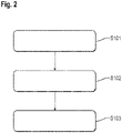
- step S101 light for curing the light-curing material 121 is emitted by the light source 101.
- FIG. The actual value of the light intensity of the emitted light is then determined by the sensor 103 in step S102.
- step S103 the electric current through the light source 101 is increased or decreased until the actual value of the light intensity reaches the predetermined target value.
- the method allows the light intensity for curing the light-curing material 121 to be set to the desired size precisely and constantly over time. Since the sensor 103 is subject to little age-related deterioration, the light intensity can be adjusted to a predetermined value with high accuracy.
- All method steps can be implemented by devices that are suitable for carrying out the respective method step. All functions performed by physical features can be a method step of a method.
Landscapes
- Chemical & Material Sciences (AREA)
- Engineering & Computer Science (AREA)
- Materials Engineering (AREA)
- Manufacturing & Machinery (AREA)
- Physics & Mathematics (AREA)
- Optics & Photonics (AREA)
- Mechanical Engineering (AREA)
- Health & Medical Sciences (AREA)
- Toxicology (AREA)
- General Physics & Mathematics (AREA)
Description
- Die vorliegende Erfindung betrifft ein Stereolithografiegerät und ein Verfahren zum Einstellen eines Stereolithografiegerätes.
- Die Stereolithografie (SLA) ist ein dreidimensionales Druckverfahren, bei dem ein Werkstück aus einem Flüssigbad aus einem Photopolymer schrittweise aufgebaut wird, oder das Werkstück in einem Flüssigbad mittels einer Bauplattform erstellt wird. Die Bauplattform wird zunächst in das Flüssigkeitsbad eingeführt und nach einem Bilden einzelner Schichten aus dem Flüssigkeitsbad ausgeführt. Anschließend wird die Bauplattform wieder ins Flüssigbad eingeführt, bis das gewünschte Objekt hergestellt ist. Ein Lichtmuster wird bei jedem Schritt auf das Photopolymer projiziert. An den Stellen, an denen das Lichtmuster auf das Photopolymer trifft, härtet dieses aus. Auf diese Weise kann das Werkstück schichtweise mit der gewünschten Form hergestellt werden.
- Eine Ultraviolett-Lichtquelle (z.B. LED) des Stereolithografiegerätes ist über die geforderte Lebensdauer von Alterungseffekten betroffen, so dass die Lichtintensität bei gleichbleibendem elektrischem Strom abnimmt. Auch andere Komponenten im Lichtpfad, wie Prismen, Linsen, Lichtmischstäbe und elektronische Spiegelgeräte, zeigen durch die hohe Bestrahlung mit UV-Licht Degradierungseffekte, die sich in einer verminderten Bestrahlungsintensität auf dem Baufeld manifestieren. Für die Qualität des Bauprozesses ist es jedoch von entscheidender Wichtigkeit, dass die Lichtintensität über die gesamte Lebensdauer des Stereolithografiegerätes konstant bleibt. Die Druckschrift
EP 18 190 700.7 - Die Druckschrift
EP 1 894 704 A1 betrifft eine Technik, um eine verbesserte Wandglattheit und Merkmalsgenauigkeit in einem Bildprojektionssystem zu erhalten, die durch die projizierte Größe der Bildpunkte erhalten wird. - Die Druckschrift
WO 2013/170311 A1 betrifft ein Gerät zum Herstellen eines Objekts. Das Gerät umfasst eine Strahlungsquelle, wie zum Beispiel eine Leuchtdiode. Ein Prisma richtet die Strahlung auf einen räumlichen Lichtmodulator (Spatial Light Modulator - SLM), wie beispielsweise ein DLP mikro-elektromechanisches System (MEMS). - Die Druckschrift
EP 3 470 210 A1 (Stand der Technik nach Art. 54(3) EPÜ) betrifft ein 3D-Druckgerät. Das 3D-Druckgerät umfasst eine Lichtquelle 110 und ein digitales Spiegelgerät. Ein Teil des Lichtes trifft auf erste Mikrospiegel auf, die diesen Teil auf die Arbeitsflüssigkeit lenken, um diese Auszuhärten und das 3D-Druckobjekt zu erzeugen. - Die Druckschrift
US 2018/186066 A1 betrifft ein Gerät zum Herstellen eines dreidimensionalen Artikels. Eine Lichtmaschine 10 ist konfiguriert, um ein Pixelbild auf eine Aufbauebene zu projizieren. Ein Sensor erfasst die Intensität für jeden Pixel in der gesamten Aufbauebene. - Das Problem wurde bisher entweder ignoriert oder mit einer Alterungskompensation gelöst, bei der die Belichtungszeit und/oder die Stromstärke der Lichtquelle mit einer fest hinterlegten Charakteristik über die Dauer angepasst werden. Die hinterlegte Charakteristik berücksichtigt jedoch die Exemplarstreuung der verwendeten Komponenten nicht. Die Steuerung der Lichtintensität über die Alterungscharakteristik der Lichtquelle und das nicht-vorhersehbare Alterungsverhalten des restlichen Lichtpfads ist daher ungenau.
- Es ist daher die technische Aufgabe der vorliegenden Erfindung, eine Lichtintensität in einem Stereolithografiegerät mit hoher Genauigkeit über die Lebensdauer hinweg aufrecht zu erhalten.
- Diese Aufgabe wird durch Gegenstände nach den unabhängigen Ansprüchen gelöst. Vorteilhafte Ausführungsformen sind Gegenstand der abhängigen Ansprüche, der Beschreibung und der Figuren.
- Gemäß einem ersten Aspekt wird diese Aufgabe durch ein Stereolithografiegerät gelöst, mit einer Lichtquelle zum Aussenden von Licht zum Aushärten eines lichtaushärtenden Materials; einem Sensor zum Bestimmen eines Istwertes der Lichtintensität des ausgesandten Lichtes; und einer Steuereinheit zum Anpassen des elektrischen Stromes durch die Lichtquelle bis der Istwert der Lichtintensität einen vorgegebenen Sollwert erreicht, wobei das Stereolithografiegerät ausgebildet ist, das Licht von der Lichtquelle zum Sensor über ein digitales Spiegelgerät umzulenken, das zur Projektion eines Lichtmusters auf das lichtaushärtende Material dient. Da der Sensor keine Alterungserscheinungen aufweist, kann die Lichtintensität mittels eines geschlossenen Regelkreises (Closed Loop) auf exakt den vorgegebenen Sollwert der Lichtintensität eingeregelt werden. Dadurch können auch Alterungserscheinungen mittels Ausgasungen bei Bestrahlung oder Erwärmung von Kunststoffteilen, allgemeiner Umwelteinflüsse oder Ablagerungen beim Herstellprozess der übrigen Komponenten, wie Prismen, Linsen, Lichtmischstäbe und des digitalen Spiegelgeräts (DMD), innerhalb des Lichtpfades kompensiert werden. Es wird eine zeitlich konstante Lichtintensität und eine erhöhte Lebensdauer des Stereolithografiegerätes erreicht. Dadurch wird beispielsweise der technische Vorteil erreicht, dass das Licht bedarfsweise auf einen Auskopplungslichtpfad gelenkt werden kann und sich die Lebensdauer des Sensors erhöht.
- In einer weiteren technisch vorteilhaften Ausführungsform des Stereolithografiegerätes ist das digitale Spiegelgerät benachbart zu einer Prismafläche angeordnet. Dadurch wird beispielsweise der technische Vorteil erreicht, dass die Bauform des Stereolithografiegerätes verkleinert werden kann.
- In einer weiteren technisch vorteilhaften Ausführungsform des Stereolithografiegerätes ist das Stereolithografiegerät ausgebildet, ein vorgegebenes Lichtmuster durch das digitales Spiegelgerät auf den Sensor zu projizieren. Dadurch wird beispielsweise der technische Vorteil erreicht, dass die Lichtmenge auf den Sensor genau dosiert werden kann.
- In einer weiteren technisch vorteilhaften Ausführungsform des Stereolithografiegerätes umfasst das Stereolithografiegerät eine Spiegelfläche zum Umlenken des Lichts auf den Sensor. Dadurch wird beispielsweise der technische Vorteil erreicht, dass der Sensor flexibel an unterschiedlichen Positionen im Inneren des Stereolithografiegerätes angeordnet werden kann.
- In einer weiteren technisch vorteilhaften Ausführungsform des Stereolithografiegerätes ist die Spiegelfläche benachbart zu einer Prismablende angeordnet. Dadurch wird beispielsweise der technische Vorteil erreicht, dass die Prismablende eine vorgegebene Austrittsöffnung definiert und ungewolltes Streulicht reduziert wird.
- In einer weiteren technisch vorteilhaften Ausführungsform des Stereolithografiegerätes ist der Sensor speziell zum Erfassen von ultraviolettem Licht ausgebildet. Dadurch wird beispielsweise der technische Vorteil erreicht, dass eine hohe Lebensdauer des Sensors erreicht wird.
- In einer weiteren technisch vorteilhaften Ausführungsform des Stereolithografiegerätes ist der Sensor durch eine Photodiode gebildet. Dadurch wird beispielsweise der technische Vorteil erreicht, dass der Sensor kostengünstig ist und gleichzeitig geringe Alterungserscheinungen aufweist.
- In einer weiteren technisch vorteilhaften Ausführungsform des Stereolithografiegerätes umfasst die Steuereinheit einen Regler zum Regeln des Stromes durch die Lichtquelle, wie beispielsweise einen PID-Regler oder PI-Regler. Dadurch wird beispielsweise der technische Vorteil erreicht, dass eine schnelle und effiziente Regelung des Regelkreises durchgeführt wird.
- Gemäß einem zweiten Aspekt wird diese Aufgabe durch ein Verfahren zum Einstellen eines Stereolithografiegerätes gelöst, mit den Schritten eines Aussendens von Licht zum Aushärten eines lichtaushärtenden Materials mittels einer Lichtquelle; eines Bestimmens eines Istwertes der Lichtintensität des ausgesandten Lichtes; und eines Anpassens des elektrischen Stromes durch die Lichtquelle bis der Istwert der Lichtintensität einen vorgegebenen Sollwert erreicht. Durch das Verfahren werden die gleichen technischen Vorteile wie durch das Stereolithografiegerät nach dem ersten Aspekt erreicht, wobei das Licht von der Lichtquelle zum Sensor durch ein digitales Spiegelgerät umgelenkt, das zur Projektion eines Lichtmusters auf das lichtaushärtende Material dient. Dadurch wird beispielsweise ebenfalls der technische Vorteil erreicht, dass das Licht bedarfsweise auf einen Auskopplungslichtpfad gelenkt werden kann und sich die Lebensdauer des Sensors erhöht.
- In einer weiteren technisch vorteilhaften Ausführungsform des Verfahrens wird ein vorgegebenes Lichtmuster durch das digitale Spiegelgerät auf den Sensor projiziert. Dadurch wird beispielsweise ebenfalls der technische Vorteil erreicht, dass das auf den Sensor eintreffende Licht dosiert werden kann.
- In einer weiteren technisch vorteilhaften Ausführungsform des Verfahrens wird das Licht über eine Spiegelfläche auf den Sensor umgelenkt. Dadurch wird beispielsweise ebenfalls der technische Vorteil erreicht, dass der Sensor flexibel an unterschiedlichen Positionen im Inneren des Stereolithografiegerätes angeordnet werden kann.
- In einer weiteren technisch vorteilhaften Ausführungsform des Verfahrens wird der Strom durch einen Regler auf den Sollwert geregelt wird, wie beispielsweise einem PID-Regler.
- Dadurch wird beispielsweise ebenfalls der technische Vorteil erreicht, dass eine schnelle und effiziente Regelung des Regelkreises durchgeführt wird.
- In einer weiteren technisch vorteilhaften Ausführungsform des Verfahrens wird das Licht durch eine Prismablende geführt. Dadurch wird beispielsweise ebenfalls der technische Vorteil erreicht, dass die Prismablende eine vorgegebene Austrittsöffnung definiert und das Bestimmen des Istwertes bei unterschiedlichen Messungen in vergleichbarer Weise durchgeführt wird. Ausführungsbeispiele der Erfindung sind in den Zeichnungen dargestellt und werden im Folgenden näher beschrieben.
- Es zeigen:
- Fig. 1
- eine schematische Darstellung eines Stereolithografiegerätes; und
- Fig. 2
- ein Blockdiagramm eines Verfahrens zum Einstellen eines Stereolithografiegerätes.
-
Fig. 1 zeigt eine schematische Darstellung eines Stereolithografiegerätes 100. Das Stereolithografiegerät 100 dient zum Herstellen von Werkstücken mittels eines dreidimensionalen Druckverfahrens (3D-Druck). Das Werkstück befindet sich hierzu in einem Flüssigbad aus einem lichtaushärtenden Material, wie beispielsweise einem Photopolymer, das schrittweise aufgebaut wird. Bei jedem Schritt wird ein spezielles Lichtmuster 123 auf das lichtaushärtende Material 121 projiziert. An den Stellen, an denen das Lichtmuster 123 auf das lichtaushärtende Material trifft, härtet dieses aus und wird fest. Auf diese Weise kann das Werkstück schichtweise mit der gewünschten Form hergestellt werden. - Das Stereolithografiegerät 100 umfasst eine Lichtquelle 101, wie beispielsweise eine Ultraviolett-LED (UV-LED), die zum Erzeugen des Lichtes dient, das das Material aushärtet. Weiter umfasst das Stereolithografiegerät 100 einen geschlossenen Regelkreis (Closed Loop), mit dem die Lichtintensität gemessen wird und eine Kompensation der Lichtintensität anhand der gewonnenen Messdaten durchgeführt wird. Auf diese Weise kann ein geschlossener Regelkreis realisiert werden, der eine genaue Einstellung der Lichtintensität über die gesamte Lebensdauer des Stereolithografiegerätes 100 anhand eines voreingestellten Sollwertes ermöglicht und mit dem Alterungseffekte der optischen Komponenten kompensiert werden können. Zusätzlich kann mittels eines Temperaturfühlers der Widerstand der Leuchtdiode gemessen werden und die Bestromung entsprechend angepasst werden, so dass sich zusätzlich die Lebensdauer der Leuchtdiode erhöht. Steigt beispielsweise die gemessene Temperatur, sinkt der Widerstand der Leuchtdiode. In diesem Fall würde ein zu hoher Strom durch die Leuchtdiode fließen.
- Zu diesem Zweck wird das von der Lichtquelle 101 ausgesendete Licht beispielsweise mit einem digitalen Spiegelgerät (Digital Micromirror Device - DMD) 113 auf einen Auskopplungslichtpfad 107 gelenkt. Das Digital Micromirror Device 113 umfasst eine Vielzahl von matrixförmig angeordneten Mikrospiegelaktoren, die einzeln mittels elektrischer Spannungen ansteuerbar sind und verkippt werden können. Jeder einzelne dieser Mikrospiegelaktoren kann daher das auftreffende Licht in Richtung des lichtaushärtenden Materials 121 oder in Richtung des Auskopplungslichtpfades 107 auf den Sensor 103 lenken. Auf diese Wiese lassen sich die Lichtmuster 123 erzeugen, die das lichtaushärtende Material 121 verfestigen.
- Dadurch kann das gesamte Licht oder lediglich bestimmte Lichtmuster auf den Sensor 103 gelenkt werden. Eine Auskopplung des Lichts kann lediglich für eine bestimmte vordefinierte Zeitdauer während einem Kalibriervorgang erfolgen, so dass der Sensor 103 nur in diesem Zeitraum der Beleuchtung ausgesetzt ist. Der Kalibriervorgang kann beispielsweise nach jeder Schicht (Slice) während eines Bauprozesses, nach einer vorgegebenen Anzahl von Schichten (Iterationen), nach jedem Bauteil oder nach jedem Wartungsvorgang oder Service durchgeführt werden.
- Über eine reflektierende Spiegelfläche 109 beim Niederhalter 115 der Prismablende 117 wird das ausgekoppelte Licht auf den Sensor 103 gelenkt. Die Prismablende 117 definiert eine flächenmäßig vorgegebene Austrittsöffnung auf der Oberfläche des Prismas 111, so dass der Auskopplungslichtpfad 107 seitlich begrenzt und so das ungewollte Streulicht reduziert wird. Durch die Spiegelfläche 109 wird das Licht auf den Sensor 103 umgelenkt, so dass dieser direkt oberhalb des Prismas 111 angeordnet sein kann. Dadurch lässt sich der Sensor 103 auch an Stellen innerhalb des Stereolithografiegerätes 100 anordnen, die nicht in der ursprünglichen Ausbreitungsrichtung des Auskopplungslichtpfades 107 liegen.
- Der Sensor 103 ist derart ausgebildet, dass dieser speziell für das beim Stereolithographieverfahren eingesetzte Licht geeignet ist und keine Verschlechterung der Messung über die Lebensdauer hinweg auftritt. Hierzu ist der Sensor 103 beispielsweise aus einer Photodiode gebildet. Im Allgemeinen können aber auch andere Sensoren 103 verwendet werden.
- Die Messunsicherheit wird dadurch kompensiert, dass beim Messvorgang der gemessene Istwert der Lichtintensität als Führungsgröße beispielsweise in einen PID-Regler (Proportional-Integral-Derivative Controller) 119 geführt wird, der in einer Steuereinheit 105 angeordnet ist. Der PID-Regler ist eine Kombination aus einem proportional wirkenden Regler (P-Regler), einem integralwirkenden Regler (I-Regler) und einem differential wirkenden Regler (D-Regler).
- Der proportionalwirkende Regler multipliziert die Regelabweichung mit seinem Verstärkungsfaktor. Der integralwirkende Regler summiert die Regelabweichung über der Zeit auf und multipliziert die Summe (d.h. das Integral) mit einem Faktor. Der differential wirkende Regler bewertet (differenziert) die Änderung einer Regelabweichung und berechnet so deren Änderungsgeschwindigkeit. Der PID-geregelte Kreis ermöglicht eine genaue und schnelle Stromeinstellung auf den vorgegebenen Sollwert. Im Allgemeinen können aber auch andere Regler zum Einregeln der Lichtintensität verwendet werden.
- Der Sollwert kann als digitaler Wert bei der Herstellung des Stereolithografiegerätes 100 gerätespezifisch in einem nichtflüchtigen Datenspeicher 125 abgespeichert werden, wie beispielsweise einem Flash-Speicher. Der Istwert der Lichtintensität kann ebenfalls digital erfasst werden und mit dem gespeicherten Sollwert verglichen werden. Je nach Abweichung zwischen dem Istwert und dem Sollwert kann der elektrische Strom durch die Lichtquelle 101 solange erhöht oder verringert werden, bis der Istwert der Lichtintensität dem gespeicherten Sollwert entspricht. Die Anpassung des Stromwertes kann beispielsweise über eine Pulsbreitenmodulation oder Amplitudenmodulation erfolgen.
- Durch den elektronischen PID-Regler oder PI-Regler 119 wird somit die Lichtintensität mittels einer Stromregelung für die Lichtquelle 101 auf den geforderten Sollwert geregelt. Auf diese Weise können eine Alterungskompensation und ein Kalibrierungsvorgang über den PID-Regler 119 schnell und effizient durchgeführt werden. Im Allgemeinen sind jedoch auch andere Regelmechanismen mit geschlossener Schleife möglich, um die Lichtintensität des Stereolithografiegerätes 100 auf einen vorgegebenen Sollwert einzuregeln.
- Während der Messung regelt der PID-Regler 119 die Lichtintensität der Lichtquelle 101, bis diese den vorgegebenen Sollwert erreicht. Dieser Sollwert dient als Referenzwert und wird beispielsweise bei der anfänglichen Kalibrierung des Stereolithografiegerätes 100 in der Produktion bestimmt. Der für das Erreichen des Sollwertes nötige Stromwert wird von der Steuereinheit 105 an das Stereolithografiegerät 100 zurückgegeben und als neuer Referenzwert für den Strom benutzt.
-
Fig. 2 zeigt ein Blockdiagramm eines Verfahrens zum Einstellen des Stereolithografiegerätes 100. In Schritt S101 wird Licht zum Aushärten des lichtaushärtenden Materials 121 mittels der Lichtquelle 101 ausgesandt. Anschließend wird in Schritt S102 der Istwert der Lichtintensität des ausgesandten Lichtes durch den Sensor 103 bestimmt. In Schritt S103 wird der elektrische Strom durch die Lichtquelle 101 solange erhöht oder verringert, bis der Istwert der Lichtintensität den vorgegebenen Sollwert erreicht. Durch das Verfahren lässt sich die Lichtintensität zum Aushärten des lichtaushärtenden Materials 121 exakt und zeitlich konstant auf die gewünschte Größe einstellen. Da der Sensor 103 nur einer geringen altersbedingten Verschlechterung unterliegt, kann die Lichtintensität mit hoher Genauigkeit auf einen vorgegebenen Wert eingeregelt werden. - Alle in Verbindung mit einzelnen Ausführungsformen der Erfindung erläuterten und gezeigten Merkmale können in unterschiedlicher Kombination in dem erfindungsgemäßen Gegenstand vorgesehen sein, um gleichzeitig deren vorteilhafte Wirkungen zu realisieren.
- Alle Verfahrensschritte können durch Vorrichtungen implementiert werden, die zum Ausführen des jeweiligen Verfahrensschrittes geeignet sind. Alle Funktionen, die von gegenständlichen Merkmalen ausgeführt werden, können ein Verfahrensschritt eines Verfahrens sein.
- Der Schutzbereich der vorliegenden Erfindung ist durch die Ansprüche gegeben und wird durch die in der Beschreibung erläuterten oder den Figuren gezeigten Merkmale nicht beschränkt.
-
- 100
- Stereolithografiegerät
- 101
- Lichtquelle
- 103
- Sensor
- 105
- Steuereinheit
- 107
- Auskopplungslichtpfad
- 109
- Spiegelfläche
- 111
- Prisma
- 113
- digitales Spiegelgerät / Digital Micromirror Device
- 115
- Niederhalter
- 117
- Prismablende
- 119
- PID-Regler
- 121
- lichtaushärtendes Material
- 123
- Lichtmuster
- 125
- Datenspeicher
Claims (13)
- Stereolithografiegerät (100), mit:einer Lichtquelle (101) zum Aussenden von Licht zum Aushärten eines lichtaushärtenden Materials (121);einem Sensor (103) zum Bestimmen eines Istwertes der Lichtintensität des ausgesandten Lichtes; undeiner Steuereinheit (105) zum Anpassen des elektrischen Stromes durch die Lichtquelle (101) bis der Istwert der Lichtintensität einen vorgegebenen Sollwert erreicht;wobei das Stereolithografiegerät (100) ausgebildet ist, das Licht von der Lichtquelle (101) zum Sensor (103) über ein digitales Spiegelgerät (113) umzulenken, das zur Projektion eines Lichtmusters (123) auf das lichtaushärtende Material (121) dient, und wobei das Stereolithografiegerät (100) so angepasst ist, dass eine Auskopplung des Lichts lediglich für eine bestimmte vordefinierte Zeitdauer während einem Kalibriervorgang erfolgt, so dass der Sensor (103) nur in diesem Zeitraum der Beleuchtung ausgesetzt ist.
- Stereolithografiegerät (100) nach Anspruch 1, wobei das digitale Spiegelgerät (113) benachbart zu einer Prismafläche angeordnet ist.
- Stereolithografiegerät (100) nach Anspruch 1 oder 2, wobei das Stereolithografiegerät (100) ausgebildet ist, ein vorgegebenes Lichtmuster durch das digitale Spiegelgerät (113) auf den Sensor (103) zu projizieren.
- Stereolithografiegerät (100) nach einem der vorangehenden Ansprüche, wobei das Stereolithografiegerät (100) eine Spiegelfläche (109) zum Umlenken des Lichts auf den Sensor (103) umfasst.
- Stereolithografiegerät (100) nach Anspruch 4, wobei die Spiegelfläche (109) benachbart zu einer Prismablende (117) angeordnet ist.
- Stereolithografiegerät (100) nach einem der vorangehenden Ansprüche, wobei der Sensor (103) speziell zum Erfassen von dem im Stereolithografiegerät eingesetzten Lichtspektrum ausgebildet ist.
- Stereolithografiegerät (100) nach Anspruch 6, wobei der Sensor (103) durch eine Photodiode gebildet ist.
- Stereolithografiegerät (100) nach einem der vorangehenden Ansprüche, wobei die Steuereinheit (105) einen Regler (119) zum Regeln des Stromes durch die Lichtquelle (101) umfasst.
- Verfahren zum Einstellen eines Stereolithografiegerätes (100), mit den Schritten:- Aussenden (S101) von Licht zum Aushärten eines lichtaushärtenden Materials (121) mittels einer Lichtquelle (101) ;- Bestimmen (S102) eines Istwertes der Lichtintensität des ausgesandten Lichtes; und- Anpassen (S103) des elektrischen Stromes durch die Lichtquelle (101) bis der Istwert der Lichtintensität einen vorgegebenen Sollwert erreicht;wobei das Licht von der Lichtquelle (101) zum Sensor (103) durch ein digitales Spiegelgerät (113) umgelenkt wird, das zur Projektion eines Lichtmusters (123) auf das lichtaushärtende Material (121) dient und eine Auskopplung des Lichts lediglich für eine bestimmte vordefinierte Zeitdauer während einem Kalibriervorgang erfolgt, so dass der Sensor (103) nur ein diesem Zeitraum der Beleuchtung ausgesetzt ist.
- Verfahren nach Anspruch 9, wobei ein vorgegebenes Lichtmuster durch das digitale Spiegelgerät (113) auf den Sensor (103) projiziert wird.
- Verfahren nach einem der Ansprüche 9 oder 10, wobei das Licht über eine Spiegelfläche (109) auf den Sensor (103) umgelenkt wird.
- Verfahren nach einem der Ansprüche 9 bis 11, wobei der Strom durch einen Regler (119) auf den Sollwert geregelt wird.
- Verfahren nach einem der Ansprüche 9 bis 12, wobei das Licht durch eine Prismablende (117) geführt wird.
Priority Applications (6)
| Application Number | Priority Date | Filing Date | Title |
|---|---|---|---|
| EP19159596.6A EP3702130B1 (de) | 2019-02-27 | 2019-02-27 | Stereolithografiegerät und ein verfahren zum einstellen eines stereolithografiegerätes |
| ES19159596T ES2916577T3 (es) | 2019-02-27 | 2019-02-27 | Dispositivo de estereolitografía y un procedimiento para ajustar un dispositivo de estereolitografía |
| CA3069929A CA3069929C (en) | 2019-02-27 | 2020-01-27 | Stereolithography device and method for adjusting a stereolithography device |
| US16/801,578 US11351722B2 (en) | 2019-02-27 | 2020-02-26 | Stereolithography device and method for adjusting a stereolithography device |
| JP2020031086A JP2020138546A (ja) | 2019-02-27 | 2020-02-26 | 光造形装置ならびに光造形装置の設定方法 |
| CN202010118237.5A CN111619105B (zh) | 2019-02-27 | 2020-02-26 | 立体光刻设备和用于调设立体光刻设备的方法 |
Applications Claiming Priority (1)
| Application Number | Priority Date | Filing Date | Title |
|---|---|---|---|
| EP19159596.6A EP3702130B1 (de) | 2019-02-27 | 2019-02-27 | Stereolithografiegerät und ein verfahren zum einstellen eines stereolithografiegerätes |
Publications (2)
| Publication Number | Publication Date |
|---|---|
| EP3702130A1 EP3702130A1 (de) | 2020-09-02 |
| EP3702130B1 true EP3702130B1 (de) | 2022-05-18 |
Family
ID=65628618
Family Applications (1)
| Application Number | Title | Priority Date | Filing Date |
|---|---|---|---|
| EP19159596.6A Active EP3702130B1 (de) | 2019-02-27 | 2019-02-27 | Stereolithografiegerät und ein verfahren zum einstellen eines stereolithografiegerätes |
Country Status (6)
| Country | Link |
|---|---|
| US (1) | US11351722B2 (de) |
| EP (1) | EP3702130B1 (de) |
| JP (1) | JP2020138546A (de) |
| CN (1) | CN111619105B (de) |
| CA (1) | CA3069929C (de) |
| ES (1) | ES2916577T3 (de) |
Families Citing this family (4)
| Publication number | Priority date | Publication date | Assignee | Title |
|---|---|---|---|---|
| EP4005707A1 (de) * | 2020-11-24 | 2022-06-01 | Rolls-Royce Corporation | Verdeckungsvorrichtung für ein optisches system in systemen zur generativen fertigung |
| KR102441901B1 (ko) * | 2021-05-07 | 2022-09-13 | 서울과학기술대학교 산학협력단 | 재료물성 조절이 가능한 광조형 3d 프린팅 방법 |
| US20230330935A1 (en) * | 2022-04-19 | 2023-10-19 | Carbon, Inc. | Light source variability correction in additive manufacturing |
| CN115002967B (zh) * | 2022-06-23 | 2024-07-09 | 广州黑格智造信息科技有限公司 | 三维打印设备及其光源控制方法、装置 |
Family Cites Families (21)
| Publication number | Priority date | Publication date | Assignee | Title |
|---|---|---|---|---|
| AU2001296428A1 (en) * | 2000-09-27 | 2002-04-08 | The Regents Of The University Of California | Dynamic mask projection stereo micro lithography |
| US7643746B2 (en) | 2002-11-14 | 2010-01-05 | Ccs Inc. | Light intensity adjusting system |
| JP4515853B2 (ja) * | 2004-08-04 | 2010-08-04 | ナブテスコ株式会社 | 光学的立体造形装置 |
| JP2006350131A (ja) * | 2005-06-17 | 2006-12-28 | Shinko Electric Ind Co Ltd | 光源制御装置 |
| US9415544B2 (en) * | 2006-08-29 | 2016-08-16 | 3D Systems, Inc. | Wall smoothness, feature accuracy and resolution in projected images via exposure levels in solid imaging |
| JP5211487B2 (ja) * | 2007-01-25 | 2013-06-12 | 株式会社ニコン | 露光方法及び露光装置並びにマイクロデバイスの製造方法 |
| WO2010043275A1 (en) * | 2008-10-17 | 2010-04-22 | Huntsman Advanced Materials (Switzerland) Gmbh | Improvements for rapid prototyping apparatus |
| WO2013170311A1 (en) * | 2012-05-15 | 2013-11-21 | Zydex Pty Ltd | Apparatus and method for making an object |
| US9233507B2 (en) | 2013-11-22 | 2016-01-12 | Charles Bibas | 3D printing apparatus with sensor device |
| US9386669B2 (en) | 2013-12-26 | 2016-07-05 | Lutron Electronics Co., Inc. | Controlling light intensity at a location |
| EP3101477B1 (de) * | 2014-01-28 | 2018-12-05 | Prismlab China Ltd. | Lichthärtende 3d-druckvorrichtung und bildbelichtungssystem dafür |
| US9459580B2 (en) | 2014-02-10 | 2016-10-04 | Xerox Corporation | Optical sensor with multiple detect modes |
| KR101624035B1 (ko) * | 2014-06-13 | 2016-05-25 | 서울과학기술대학교 산학협력단 | 광경화성 수지를 이용한 3차원 인쇄 장치 |
| US10207489B2 (en) | 2015-09-30 | 2019-02-19 | Sigma Labs, Inc. | Systems and methods for additive manufacturing operations |
| CN107031035B (zh) * | 2016-02-02 | 2019-07-12 | 三纬国际立体列印科技股份有限公司 | 立体物件成型系统及其校正方法 |
| EP3562649B1 (de) * | 2016-12-29 | 2020-09-23 | 3D Systems, Inc. | Sensor zur simulation von optischen harzeigenschaften |
| US10234848B2 (en) | 2017-05-24 | 2019-03-19 | Relativity Space, Inc. | Real-time adaptive control of additive manufacturing processes using machine learning |
| CN110770626B (zh) * | 2017-06-21 | 2022-04-01 | 依视路国际公司 | 光学物品的制造方法和光学成形设备 |
| CN107053663B (zh) * | 2017-06-27 | 2019-11-19 | 上海联泰三维科技有限公司 | 光学系统、照射控制方法及所适用的3d打印设备 |
| CN109664502A (zh) * | 2017-10-16 | 2019-04-23 | 三纬国际立体列印科技股份有限公司 | 立体打印装置 |
| US10532577B1 (en) | 2018-11-07 | 2020-01-14 | Electronics For Imaging, Inc. | Unitary ink tank for printer system |
-
2019
- 2019-02-27 EP EP19159596.6A patent/EP3702130B1/de active Active
- 2019-02-27 ES ES19159596T patent/ES2916577T3/es active Active
-
2020
- 2020-01-27 CA CA3069929A patent/CA3069929C/en active Active
- 2020-02-26 JP JP2020031086A patent/JP2020138546A/ja active Pending
- 2020-02-26 US US16/801,578 patent/US11351722B2/en active Active
- 2020-02-26 CN CN202010118237.5A patent/CN111619105B/zh active Active
Also Published As
| Publication number | Publication date |
|---|---|
| CA3069929A1 (en) | 2020-08-27 |
| EP3702130A1 (de) | 2020-09-02 |
| JP2020138546A (ja) | 2020-09-03 |
| CN111619105A (zh) | 2020-09-04 |
| CN111619105B (zh) | 2023-07-28 |
| ES2916577T3 (es) | 2022-07-01 |
| US11351722B2 (en) | 2022-06-07 |
| CA3069929C (en) | 2026-03-17 |
| US20200269492A1 (en) | 2020-08-27 |
Similar Documents
| Publication | Publication Date | Title |
|---|---|---|
| EP3702130B1 (de) | Stereolithografiegerät und ein verfahren zum einstellen eines stereolithografiegerätes | |
| EP3383624B1 (de) | Verfahren zum kalibrieren einer vorrichtung zum herstellen eines dreidimensionalen objekts | |
| DE102014108633B9 (de) | Vorrichtung und Verfahren zur Herstellung dreidimensionaler Objekte mittels Rapid-Prototyping | |
| DE69909136T2 (de) | Rapid-prototyping-vorrichtung und rapid-prototyping-methode | |
| EP3363621B1 (de) | Verfahren und vorrichtung zur belichtungssteuerung einer selektiven lasersinter- oder laserschmelzvorrichtung | |
| DE69811861T2 (de) | Optisches herstellungsverfahren und - gerät | |
| DE69218572T2 (de) | Stereolithographische Vorrichtung und Verfahren zur Herstellung eines Modells | |
| DE102014012286B4 (de) | Vorrichtung und Verfahren zum Herstellen von dreidimensionalen Objekten | |
| EP3625029B1 (de) | Messsystem für eine vorrichtung zum generativen herstellen eines dreidimensionalen objekts | |
| DE60020895T2 (de) | Stereolithografische Verfahren und Vorrichtung mit Kontrolle der vorgeschriebenen Anregung | |
| WO2018014948A1 (de) | 3d-druckvorrichtung und verfahren zum herstellen von objekten | |
| WO1992011577A1 (de) | Verfahren und vorrichtung zum herstellen eines dreidimensionalen objekts | |
| DE4112695C2 (de) | ||
| DE102006019964A1 (de) | Vorrichtung und Verfahren zur Herstellung eines dreidimensionalen Objekts mittels Maskenbelichtung | |
| DE102014108634A1 (de) | Effizienteres Verfahren zur Herstellung dreidimensionaler Objekte mittels Rapid-Prototyping | |
| EP3962713B1 (de) | 3d-druckvorrichtung zur photopolymerisation eines photosensitiven kunstharzes durch ein belichtungsmuster | |
| DE102014010412A1 (de) | Verfahren und Anordnung zur generativen Fertigung von Bauteilen | |
| DE102007022895B9 (de) | Vorrichtung zum Übertragen von in einer Maske vorgesehenen Strukturen auf ein Substrat | |
| WO2021185925A1 (de) | Verfahren zur kalibrierung von inkjet-düsen in einer druckvorrichtung und eine druckvorrichtung zum betrieb mit einem solchen verfahren | |
| AT523222B1 (de) | Nachbelichtungseinheit | |
| DE10143218A1 (de) | Verfahren und Vorrichtung zum Drucken 3D-modellierter Objekte | |
| DE102015115231B4 (de) | Verfahren und Vorrichtung zur Herstellung 3-dimensionaler Modelle mit einem strahlungshärtendem Kunststoff | |
| DE112022004780T5 (de) | Laserstrahlmaschine und Verfahren zum Steuern einer Laserstrahlmaschine | |
| DE102024130813A1 (de) | Fertigungsverfahren zur additiven Fertigung von Fertigungsprodukten | |
| DE102013225694A1 (de) | Optisches modul |
Legal Events
| Date | Code | Title | Description |
|---|---|---|---|
| PUAI | Public reference made under article 153(3) epc to a published international application that has entered the european phase |
Free format text: ORIGINAL CODE: 0009012 |
|
| STAA | Information on the status of an ep patent application or granted ep patent |
Free format text: STATUS: THE APPLICATION HAS BEEN PUBLISHED |
|
| AK | Designated contracting states |
Kind code of ref document: A1 Designated state(s): AL AT BE BG CH CY CZ DE DK EE ES FI FR GB GR HR HU IE IS IT LI LT LU LV MC MK MT NL NO PL PT RO RS SE SI SK SM TR |
|
| AX | Request for extension of the european patent |
Extension state: BA ME |
|
| STAA | Information on the status of an ep patent application or granted ep patent |
Free format text: STATUS: REQUEST FOR EXAMINATION WAS MADE |
|
| 17P | Request for examination filed |
Effective date: 20201028 |
|
| RBV | Designated contracting states (corrected) |
Designated state(s): AL AT BE BG CH CY CZ DE DK EE ES FI FR GB GR HR HU IE IS IT LI LT LU LV MC MK MT NL NO PL PT RO RS SE SI SK SM TR |
|
| STAA | Information on the status of an ep patent application or granted ep patent |
Free format text: STATUS: EXAMINATION IS IN PROGRESS |
|
| 17Q | First examination report despatched |
Effective date: 20210323 |
|
| GRAP | Despatch of communication of intention to grant a patent |
Free format text: ORIGINAL CODE: EPIDOSNIGR1 |
|
| STAA | Information on the status of an ep patent application or granted ep patent |
Free format text: STATUS: GRANT OF PATENT IS INTENDED |
|
| INTG | Intention to grant announced |
Effective date: 20211210 |
|
| GRAJ | Information related to disapproval of communication of intention to grant by the applicant or resumption of examination proceedings by the epo deleted |
Free format text: ORIGINAL CODE: EPIDOSDIGR1 |
|
| STAA | Information on the status of an ep patent application or granted ep patent |
Free format text: STATUS: EXAMINATION IS IN PROGRESS |
|
| INTC | Intention to grant announced (deleted) | ||
| GRAP | Despatch of communication of intention to grant a patent |
Free format text: ORIGINAL CODE: EPIDOSNIGR1 |
|
| STAA | Information on the status of an ep patent application or granted ep patent |
Free format text: STATUS: GRANT OF PATENT IS INTENDED |
|
| INTG | Intention to grant announced |
Effective date: 20220309 |
|
| GRAS | Grant fee paid |
Free format text: ORIGINAL CODE: EPIDOSNIGR3 |
|
| GRAA | (expected) grant |
Free format text: ORIGINAL CODE: 0009210 |
|
| STAA | Information on the status of an ep patent application or granted ep patent |
Free format text: STATUS: THE PATENT HAS BEEN GRANTED |
|
| AK | Designated contracting states |
Kind code of ref document: B1 Designated state(s): AL AT BE BG CH CY CZ DE DK EE ES FI FR GB GR HR HU IE IS IT LI LT LU LV MC MK MT NL NO PL PT RO RS SE SI SK SM TR |
|
| REG | Reference to a national code |
Ref country code: GB Ref legal event code: FG4D Free format text: NOT ENGLISH |
|
| REG | Reference to a national code |
Ref country code: CH Ref legal event code: EP |
|
| REG | Reference to a national code |
Ref country code: IE Ref legal event code: FG4D Free format text: LANGUAGE OF EP DOCUMENT: GERMAN |
|
| REG | Reference to a national code |
Ref country code: DE Ref legal event code: R096 Ref document number: 502019004386 Country of ref document: DE |
|
| REG | Reference to a national code |
Ref country code: AT Ref legal event code: REF Ref document number: 1492912 Country of ref document: AT Kind code of ref document: T Effective date: 20220615 |
|
| REG | Reference to a national code |
Ref country code: ES Ref legal event code: FG2A Ref document number: 2916577 Country of ref document: ES Kind code of ref document: T3 Effective date: 20220701 |
|
| REG | Reference to a national code |
Ref country code: LT Ref legal event code: MG9D |
|
| REG | Reference to a national code |
Ref country code: NL Ref legal event code: MP Effective date: 20220518 |
|
| PG25 | Lapsed in a contracting state [announced via postgrant information from national office to epo] |
Ref country code: SE Free format text: LAPSE BECAUSE OF FAILURE TO SUBMIT A TRANSLATION OF THE DESCRIPTION OR TO PAY THE FEE WITHIN THE PRESCRIBED TIME-LIMIT Effective date: 20220518 Ref country code: PT Free format text: LAPSE BECAUSE OF FAILURE TO SUBMIT A TRANSLATION OF THE DESCRIPTION OR TO PAY THE FEE WITHIN THE PRESCRIBED TIME-LIMIT Effective date: 20220919 Ref country code: NO Free format text: LAPSE BECAUSE OF FAILURE TO SUBMIT A TRANSLATION OF THE DESCRIPTION OR TO PAY THE FEE WITHIN THE PRESCRIBED TIME-LIMIT Effective date: 20220818 Ref country code: NL Free format text: LAPSE BECAUSE OF FAILURE TO SUBMIT A TRANSLATION OF THE DESCRIPTION OR TO PAY THE FEE WITHIN THE PRESCRIBED TIME-LIMIT Effective date: 20220518 Ref country code: LT Free format text: LAPSE BECAUSE OF FAILURE TO SUBMIT A TRANSLATION OF THE DESCRIPTION OR TO PAY THE FEE WITHIN THE PRESCRIBED TIME-LIMIT Effective date: 20220518 Ref country code: HR Free format text: LAPSE BECAUSE OF FAILURE TO SUBMIT A TRANSLATION OF THE DESCRIPTION OR TO PAY THE FEE WITHIN THE PRESCRIBED TIME-LIMIT Effective date: 20220518 Ref country code: GR Free format text: LAPSE BECAUSE OF FAILURE TO SUBMIT A TRANSLATION OF THE DESCRIPTION OR TO PAY THE FEE WITHIN THE PRESCRIBED TIME-LIMIT Effective date: 20220819 Ref country code: FI Free format text: LAPSE BECAUSE OF FAILURE TO SUBMIT A TRANSLATION OF THE DESCRIPTION OR TO PAY THE FEE WITHIN THE PRESCRIBED TIME-LIMIT Effective date: 20220518 Ref country code: BG Free format text: LAPSE BECAUSE OF FAILURE TO SUBMIT A TRANSLATION OF THE DESCRIPTION OR TO PAY THE FEE WITHIN THE PRESCRIBED TIME-LIMIT Effective date: 20220818 |
|
| PG25 | Lapsed in a contracting state [announced via postgrant information from national office to epo] |
Ref country code: RS Free format text: LAPSE BECAUSE OF FAILURE TO SUBMIT A TRANSLATION OF THE DESCRIPTION OR TO PAY THE FEE WITHIN THE PRESCRIBED TIME-LIMIT Effective date: 20220518 Ref country code: PL Free format text: LAPSE BECAUSE OF FAILURE TO SUBMIT A TRANSLATION OF THE DESCRIPTION OR TO PAY THE FEE WITHIN THE PRESCRIBED TIME-LIMIT Effective date: 20220518 Ref country code: LV Free format text: LAPSE BECAUSE OF FAILURE TO SUBMIT A TRANSLATION OF THE DESCRIPTION OR TO PAY THE FEE WITHIN THE PRESCRIBED TIME-LIMIT Effective date: 20220518 Ref country code: IS Free format text: LAPSE BECAUSE OF FAILURE TO SUBMIT A TRANSLATION OF THE DESCRIPTION OR TO PAY THE FEE WITHIN THE PRESCRIBED TIME-LIMIT Effective date: 20220918 |
|
| PG25 | Lapsed in a contracting state [announced via postgrant information from national office to epo] |
Ref country code: SM Free format text: LAPSE BECAUSE OF FAILURE TO SUBMIT A TRANSLATION OF THE DESCRIPTION OR TO PAY THE FEE WITHIN THE PRESCRIBED TIME-LIMIT Effective date: 20220518 Ref country code: SK Free format text: LAPSE BECAUSE OF FAILURE TO SUBMIT A TRANSLATION OF THE DESCRIPTION OR TO PAY THE FEE WITHIN THE PRESCRIBED TIME-LIMIT Effective date: 20220518 Ref country code: RO Free format text: LAPSE BECAUSE OF FAILURE TO SUBMIT A TRANSLATION OF THE DESCRIPTION OR TO PAY THE FEE WITHIN THE PRESCRIBED TIME-LIMIT Effective date: 20220518 Ref country code: EE Free format text: LAPSE BECAUSE OF FAILURE TO SUBMIT A TRANSLATION OF THE DESCRIPTION OR TO PAY THE FEE WITHIN THE PRESCRIBED TIME-LIMIT Effective date: 20220518 Ref country code: DK Free format text: LAPSE BECAUSE OF FAILURE TO SUBMIT A TRANSLATION OF THE DESCRIPTION OR TO PAY THE FEE WITHIN THE PRESCRIBED TIME-LIMIT Effective date: 20220518 Ref country code: CZ Free format text: LAPSE BECAUSE OF FAILURE TO SUBMIT A TRANSLATION OF THE DESCRIPTION OR TO PAY THE FEE WITHIN THE PRESCRIBED TIME-LIMIT Effective date: 20220518 |
|
| REG | Reference to a national code |
Ref country code: DE Ref legal event code: R097 Ref document number: 502019004386 Country of ref document: DE |
|
| PLBE | No opposition filed within time limit |
Free format text: ORIGINAL CODE: 0009261 |
|
| STAA | Information on the status of an ep patent application or granted ep patent |
Free format text: STATUS: NO OPPOSITION FILED WITHIN TIME LIMIT |
|
| PG25 | Lapsed in a contracting state [announced via postgrant information from national office to epo] |
Ref country code: AL Free format text: LAPSE BECAUSE OF FAILURE TO SUBMIT A TRANSLATION OF THE DESCRIPTION OR TO PAY THE FEE WITHIN THE PRESCRIBED TIME-LIMIT Effective date: 20220518 |
|
| 26N | No opposition filed |
Effective date: 20230221 |
|
| PG25 | Lapsed in a contracting state [announced via postgrant information from national office to epo] |
Ref country code: SI Free format text: LAPSE BECAUSE OF FAILURE TO SUBMIT A TRANSLATION OF THE DESCRIPTION OR TO PAY THE FEE WITHIN THE PRESCRIBED TIME-LIMIT Effective date: 20220518 |
|
| P01 | Opt-out of the competence of the unified patent court (upc) registered |
Effective date: 20230607 |
|
| PG25 | Lapsed in a contracting state [announced via postgrant information from national office to epo] |
Ref country code: MC Free format text: LAPSE BECAUSE OF FAILURE TO SUBMIT A TRANSLATION OF THE DESCRIPTION OR TO PAY THE FEE WITHIN THE PRESCRIBED TIME-LIMIT Effective date: 20220518 |
|
| REG | Reference to a national code |
Ref country code: BE Ref legal event code: MM Effective date: 20230228 |
|
| PG25 | Lapsed in a contracting state [announced via postgrant information from national office to epo] |
Ref country code: LU Free format text: LAPSE BECAUSE OF NON-PAYMENT OF DUE FEES Effective date: 20230227 |
|
| REG | Reference to a national code |
Ref country code: IE Ref legal event code: MM4A |
|
| PG25 | Lapsed in a contracting state [announced via postgrant information from national office to epo] |
Ref country code: IE Free format text: LAPSE BECAUSE OF NON-PAYMENT OF DUE FEES Effective date: 20230227 |
|
| PG25 | Lapsed in a contracting state [announced via postgrant information from national office to epo] |
Ref country code: BE Free format text: LAPSE BECAUSE OF NON-PAYMENT OF DUE FEES Effective date: 20230228 |
|
| PG25 | Lapsed in a contracting state [announced via postgrant information from national office to epo] |
Ref country code: BG Free format text: LAPSE BECAUSE OF FAILURE TO SUBMIT A TRANSLATION OF THE DESCRIPTION OR TO PAY THE FEE WITHIN THE PRESCRIBED TIME-LIMIT Effective date: 20220518 |
|
| PG25 | Lapsed in a contracting state [announced via postgrant information from national office to epo] |
Ref country code: BG Free format text: LAPSE BECAUSE OF FAILURE TO SUBMIT A TRANSLATION OF THE DESCRIPTION OR TO PAY THE FEE WITHIN THE PRESCRIBED TIME-LIMIT Effective date: 20220518 |
|
| PGFP | Annual fee paid to national office [announced via postgrant information from national office to epo] |
Ref country code: AT Payment date: 20250221 Year of fee payment: 7 Ref country code: CH Payment date: 20250319 Year of fee payment: 7 |
|
| PG25 | Lapsed in a contracting state [announced via postgrant information from national office to epo] |
Ref country code: CY Free format text: LAPSE BECAUSE OF FAILURE TO SUBMIT A TRANSLATION OF THE DESCRIPTION OR TO PAY THE FEE WITHIN THE PRESCRIBED TIME-LIMIT; INVALID AB INITIO Effective date: 20190227 |
|
| PG25 | Lapsed in a contracting state [announced via postgrant information from national office to epo] |
Ref country code: HU Free format text: LAPSE BECAUSE OF FAILURE TO SUBMIT A TRANSLATION OF THE DESCRIPTION OR TO PAY THE FEE WITHIN THE PRESCRIBED TIME-LIMIT; INVALID AB INITIO Effective date: 20190227 |
|
| PG25 | Lapsed in a contracting state [announced via postgrant information from national office to epo] |
Ref country code: TR Free format text: LAPSE BECAUSE OF FAILURE TO SUBMIT A TRANSLATION OF THE DESCRIPTION OR TO PAY THE FEE WITHIN THE PRESCRIBED TIME-LIMIT Effective date: 20220518 |
|
| PGFP | Annual fee paid to national office [announced via postgrant information from national office to epo] |
Ref country code: GB Payment date: 20260224 Year of fee payment: 8 |
|
| PGFP | Annual fee paid to national office [announced via postgrant information from national office to epo] |
Ref country code: ES Payment date: 20260303 Year of fee payment: 8 |
|
| PGFP | Annual fee paid to national office [announced via postgrant information from national office to epo] |
Ref country code: DE Payment date: 20260218 Year of fee payment: 8 |
|
| PGFP | Annual fee paid to national office [announced via postgrant information from national office to epo] |
Ref country code: IT Payment date: 20260219 Year of fee payment: 8 |
|
| REG | Reference to a national code |
Ref country code: CH Ref legal event code: U11 Free format text: ST27 STATUS EVENT CODE: U-0-0-U10-U11 (AS PROVIDED BY THE NATIONAL OFFICE) Effective date: 20260416 |
|
| PGFP | Annual fee paid to national office [announced via postgrant information from national office to epo] |
Ref country code: FR Payment date: 20260225 Year of fee payment: 8 |