EP3702885B1 - Procédé de commande de chargement de batterie et dispositif électronique sur lequel ce procédé est appliqué - Google Patents
Procédé de commande de chargement de batterie et dispositif électronique sur lequel ce procédé est appliqué Download PDFInfo
- Publication number
- EP3702885B1 EP3702885B1 EP20158411.7A EP20158411A EP3702885B1 EP 3702885 B1 EP3702885 B1 EP 3702885B1 EP 20158411 A EP20158411 A EP 20158411A EP 3702885 B1 EP3702885 B1 EP 3702885B1
- Authority
- EP
- European Patent Office
- Prior art keywords
- battery
- processor
- voltage
- external power
- voltage value
- Prior art date
- Legal status (The legal status is an assumption and is not a legal conclusion. Google has not performed a legal analysis and makes no representation as to the accuracy of the status listed.)
- Active
Links
Images



Classifications
-
- H—ELECTRICITY
- H02—GENERATION; CONVERSION OR DISTRIBUTION OF ELECTRIC POWER
- H02J—ELECTRIC POWER NETWORKS; CIRCUIT ARRANGEMENTS OR SYSTEMS FOR SUPPLYING OR DISTRIBUTING ELECTRIC POWER; SYSTEMS FOR STORING ELECTRIC ENERGY
- H02J7/00—Circuit arrangements for charging or discharging batteries or for supplying loads from batteries
- H02J7/60—Circuit arrangements for charging or discharging batteries or for supplying loads from batteries including safety or protection arrangements
-
- H—ELECTRICITY
- H02—GENERATION; CONVERSION OR DISTRIBUTION OF ELECTRIC POWER
- H02J—ELECTRIC POWER NETWORKS; CIRCUIT ARRANGEMENTS OR SYSTEMS FOR SUPPLYING OR DISTRIBUTING ELECTRIC POWER; SYSTEMS FOR STORING ELECTRIC ENERGY
- H02J7/00—Circuit arrangements for charging or discharging batteries or for supplying loads from batteries
- H02J7/90—Regulation of charging or discharging current or voltage
- H02J7/92—Regulation of charging or discharging current or voltage with prioritisation of loads or sources
-
- H—ELECTRICITY
- H02—GENERATION; CONVERSION OR DISTRIBUTION OF ELECTRIC POWER
- H02J—ELECTRIC POWER NETWORKS; CIRCUIT ARRANGEMENTS OR SYSTEMS FOR SUPPLYING OR DISTRIBUTING ELECTRIC POWER; SYSTEMS FOR STORING ELECTRIC ENERGY
- H02J7/00—Circuit arrangements for charging or discharging batteries or for supplying loads from batteries
- H02J7/90—Regulation of charging or discharging current or voltage
- H02J7/96—Regulation of charging or discharging current or voltage in response to battery voltage
-
- G—PHYSICS
- G06—COMPUTING OR CALCULATING; COUNTING
- G06F—ELECTRIC DIGITAL DATA PROCESSING
- G06F1/00—Details not covered by groups G06F3/00 - G06F13/00 and G06F21/00
- G06F1/26—Power supply means, e.g. regulation thereof
- G06F1/263—Arrangements for using multiple switchable power supplies, e.g. battery and AC
-
- H—ELECTRICITY
- H02—GENERATION; CONVERSION OR DISTRIBUTION OF ELECTRIC POWER
- H02J—ELECTRIC POWER NETWORKS; CIRCUIT ARRANGEMENTS OR SYSTEMS FOR SUPPLYING OR DISTRIBUTING ELECTRIC POWER; SYSTEMS FOR STORING ELECTRIC ENERGY
- H02J2105/00—Networks for supplying or distributing electric power characterised by their spatial reach or by the load
- H02J2105/40—Networks for supplying or distributing electric power characterised by their spatial reach or by the load characterised by the loads connecting to the networks or being supplied by the networks
- H02J2105/44—Portable electronic devices
Definitions
- the disclosure relates to a method of controlling charging of a battery and an electronic device to which the method is applied.
- an aspect of the disclosure is to provide a method of controlling charging of a battery and an electronic device to which the method is applied.
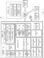
- FIG. 1 is a block diagram illustrating an electronic device in a network environment 100 to an embodiment of the disclosure.
- an electronic device 101 in a network environment 100 may communicate with an electronic device 102 via a first network 198 (e.g., a short-range wireless communication network), or an electronic device 104 or a server 108 via a second network 199 (e.g., a long-range wireless communication network).
- the electronic device 101 may communicate with the electronic device 104 via the server 108.
- the electronic device 101 may include a processor 120, memory 130, an input device 150, a sound output device 155, a display device 160, an audio module 170, a sensor module 176, an interface 177, a haptic module 179, a camera module 180, a power management module 188, a battery 189, a communication module 190, a subscriber identification module (SIM) 196, or an antenna module 197.
- at least one (e.g., the display device 160 or the camera module 180) of the components may be omitted from the electronic device 101, or one or more other components may be added in the electronic device 101.
- some of the components may be implemented as single integrated circuitry.
- the sensor module 176 e.g., a fingerprint sensor, an iris sensor, or an illuminance sensor
- the display device 160 e.g., a display
- an haptic module 179 e.g., a camera module 180
- a power management module 188 e.g., the display
- the processor 120 may execute, for example, software (e.g., a program 140) to control at least one other component (e.g., a hardware or software component) of the electronic device 101 coupled with the processor 120, and may perform various data processing or computation. According to one embodiment, as at least part of the data processing or computation, the processor 120 may load a command or data received from another component (e.g., the sensor module 176 or the communication module 190) in a volatile memory 132, process the command or the data stored in the volatile memory 132, and store resulting data in non-volatile memory 134.
- software e.g., a program 140
- the processor 120 may load a command or data received from another component (e.g., the sensor module 176 or the communication module 190) in a volatile memory 132, process the command or the data stored in the volatile memory 132, and store resulting data in non-volatile memory 134.
- the processor 120 may include a main processor 121 (e.g., a central processing unit (CPU) or an application processor (AP)), and an auxiliary processor 123 (e.g., a graphics processing unit (GPU), an image signal processor (ISP), a sensor hub processor, or a communication processor (CP)) that is operable independently from, or in conjunction with, the main processor 121.
- auxiliary processor 123 may be adapted to consume less power than the main processor 121, or to be specific to a specified function.
- the auxiliary processor 123 may be implemented as separate from, or as part of the main processor 121.
- the auxiliary processor 123 may control at least some of functions or states related to at least one component (e.g., the display device 160, the sensor module 176, or the communication module 190) among the components of the electronic device 101, instead of the main processor 121 while the main processor 121 is in an inactive (e.g., sleep) state, or together with the main processor 121 while the main processor 121 is in an active state (e.g., executing an application).
- the auxiliary processor 123 e.g., an image signal processor or a communication processor
- the memory 130 may store various data used by at least one component (e.g., the processor 120 or the sensor module 176) of the electronic device 101.
- the various data may include, for example, software (e.g., the program 140) and input data or output data for a command related thererto.
- the memory 130 may include the volatile memory 132 or the non-volatile memory 134.
- the program 140 may be stored in the memory 130 as software, and may include, for example, an operating system (OS) 142, middleware 144, or an application 146.
- OS operating system
- middleware middleware
- application application
- the input device 150 may receive a command or data to be used by other component (e.g., the processor 120) of the electronic device 101, from the outside (e.g., a user) of the electronic device 101.
- the input device 150 may include, for example, a microphone, a mouse, a keyboard, or a digital pen (e.g., a stylus pen).
- the sound output device 155 may output sound signals to the outside of the electronic device 101.
- the sound output device 155 may include, for example, a speaker or a receiver.
- the speaker may be used for general purposes, such as playing multimedia or playing record, and the receiver may be used for an incoming calls. According to an embodiment, the receiver may be implemented as separate from, or as part of the speaker.
- the display device 160 may visually provide information to the outside (e.g., a user) of the electronic device 101.
- the display device 160 may include, for example, a display, a hologram device, or a projector and control circuitry to control a corresponding one of the display, hologram device, and projector.
- the display device 160 may include touch circuitry adapted to detect a touch, or sensor circuitry (e.g., a pressure sensor) adapted to measure the intensity of force incurred by the touch.
- the audio module 170 may convert a sound into an electrical signal and vice versa. According to an embodiment, the audio module 170 may obtain the sound via the input device 150, or output the sound via the sound output device 155 or headphones of an external electronic device (e.g., an electronic device 102) directly (e.g., wiredly) or wirelessly coupled with the electronic device 101.
- an external electronic device e.g., an electronic device 102 directly (e.g., wiredly) or wirelessly coupled with the electronic device 101.
- the sensor module 176 may detect an operational state (e.g., power or temperature) of the electronic device 101 or an environmental state (e.g., a state of a user) external to the electronic device 101, and then generate an electrical signal or data value corresponding to the detected state.
- the sensor module 176 may include, for example, a gesture sensor, a gyro sensor, an atmospheric pressure sensor, a magnetic sensor, an acceleration sensor, a grip sensor, a proximity sensor, a color sensor, an infrared (IR) sensor, a biometric sensor, a temperature sensor, a humidity sensor, or an illuminance sensor.
- the interface 177 may support one or more specified protocols to be used for the electronic device 101 to be coupled with the external electronic device (e.g., the electronic device 102) directly (e.g., wiredly) or wirelessly.
- the interface 177 may include, for example, a high definition multimedia interface (HDMI), a universal serial bus (USB) interface, a secure digital (SD) card interface, or an audio interface.
- HDMI high definition multimedia interface
- USB universal serial bus
- SD secure digital
- a connecting terminal 178 may include a connector via which the electronic device 101 may be physically connected with the external electronic device (e.g., the electronic device 102).
- the connecting terminal 178 may include, for example, a HDMI connector, a USB connector, a SD card connector, or an audio connector (e.g., a headphone connector).
- the haptic module 179 may convert an electrical signal into a mechanical stimulus (e.g., a vibration or a movement) or electrical stimulus which may be recognized by a user via his tactile sensation or kinesthetic sensation.
- the haptic module 179 may include, for example, a motor, a piezoelectric element, or an electric stimulator.
- the camera module 180 may capture a still image or moving images.
- the camera module 180 may include one or more lenses, image sensors, image signal processors, or flashes.
- the power management module 188 may manage power supplied to the electronic device 101.
- the power management module 188 may be implemented as at least part of, for example, a power management integrated circuit (PMIC).
- PMIC power management integrated circuit
- the battery 189 may supply power to at least one component of the electronic device 101.
- the battery 189 may include, for example, a primary cell which is not rechargeable, a secondary cell which is rechargeable, or a fuel cell.
- the communication module 190 may support establishing a direct (e.g., wired) communication channel or a wireless communication channel between the electronic device 101 and the external electronic device (e.g., the electronic device 102, the electronic device 104, or the server 108) and performing communication via the established communication channel.
- the communication module 190 may include one or more communication processors that are operable independently from the processor 120 (e.g., the application processor (AP)) and supports a direct (e.g., wired) communication or a wireless communication.
- AP application processor
- the communication module 190 may include a wireless communication module 192 (e.g., a cellular communication module, a short-range wireless communication module, or a global navigation satellite system (GNSS) communication module) or a wired communication module 194 (e.g., a local area network (LAN) communication module or a power line communication (PLC) module).
- a wireless communication module 192 e.g., a cellular communication module, a short-range wireless communication module, or a global navigation satellite system (GNSS) communication module
- GNSS global navigation satellite system
- wired communication module 194 e.g., a local area network (LAN) communication module or a power line communication (PLC) module.
- LAN local area network
- PLC power line communication
- a corresponding one of these communication modules may communicate with the external electronic device via the first network 198 (e.g., a short-range communication network, such as Bluetooth TM , wireless-fidelity (Wi-Fi) direct, or infrared data association (IrDA)) or the second network 199 (e.g., a long-range communication network, such as a cellular network, the Internet, or a computer network (e.g., LAN or wide area network (WAN)).
- the first network 198 e.g., a short-range communication network, such as Bluetooth TM , wireless-fidelity (Wi-Fi) direct, or infrared data association (IrDA)
- the second network 199 e.g., a long-range communication network, such as a cellular network, the Internet, or a computer network (e.g., LAN or wide area network (WAN)
- These various types of communication modules may be implemented as a single component (e.g., a single chip), or may be implemented as multi
- the wireless communication module 192 may identify and authenticate the electronic device 101 in a communication network, such as the first network 198 or the second network 199, using subscriber information (e.g., international mobile subscriber identity (IMSI)) stored in the subscriber identification module 196.
- subscriber information e.g., international mobile subscriber identity (IMSI)
- the antenna module 197 may transmit or receive a signal or power to or from the outside (e.g., the external electronic device) of the electronic device 101.
- the antenna module 197 may include an antenna including a radiating element composed of a conductive material or a conductive pattern formed in or on a substrate (e.g., PCB).
- the antenna module 197 may include a plurality of antennas. In such a case, at least one antenna appropriate for a communication scheme used in the communication network, such as the first network 198 or the second network 199, may be selected, for example, by the communication module 190 (e.g., the wireless communication module 192) from the plurality of antennas.
- the signal or the power may then be transmitted or received between the communication module 190 and the external electronic device via the selected at least one antenna.
- another component e.g., a radio frequency integrated circuit (RFIC)
- RFIC radio frequency integrated circuit
- At least some of the above-described components may be coupled mutually and communicate signals (e.g., commands or data) therebetween via an inter-peripheral communication scheme (e.g., a bus, general purpose input and output (GPIO), serial peripheral interface (SPI), or mobile industry processor interface (MIPI)).
- an inter-peripheral communication scheme e.g., a bus, general purpose input and output (GPIO), serial peripheral interface (SPI), or mobile industry processor interface (MIPI)
- commands or data may be transmitted or received between the electronic device 101 and the external electronic device 104 via the server 108 coupled with the second network 199.
- Each of the electronic devices 102 and 104 may be a device of a same type as, or a different type, from the electronic device 101.
- all or some of operations to be executed at the electronic device 101 may be executed at one or more of the external electronic devices 102, 104, or 108. For example, if the electronic device 101 should perform a function or a service automatically, or in response to a request from a user or another device, the electronic device 101, instead of, or in addition to, executing the function or the service, may request the one or more external electronic devices to perform at least part of the function or the service.
- the one or more external electronic devices receiving the request may perform the at least part of the function or the service requested, or an additional function or an additional service related to the request, and transfer an outcome of the performing to the electronic device 101.
- the electronic device 101 may provide the outcome, with or without further processing of the outcome, as at least part of a reply to the request.
- a cloud computing, distributed computing, or client-server computing technology may be used, for example.
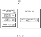
- FIG. 2 is a block diagram 200 the power management module and the battery according to an embodiment of the disclosure.
- the power management module 188 may include charging circuitry 210, a power adjuster 220, or a power gauge 230.
- the charging circuitry 210 may charge the battery 189 by using power supplied from an external power source outside the electronic device 101.
- the charging circuitry 210 may select a charging scheme (e.g., normal charging or quick charging) based at least in part on a type of the external power source (e.g., a power outlet, a USB, or wireless charging), magnitude of power suppliable from the external power source (e.g., about 20 watts or more), or an attribute of the battery 189, and may charge the battery 189 using the selected charging scheme.
- the external power source may be connected with the electronic device 101, for example, directly via the connecting terminal 178 or wirelessly via the antenna module 197.
- the power adjuster 220 may generate a plurality of powers having different voltage levels or different current levels by adjusting a voltage level or a current level of the power supplied from the external power source or the battery 189.
- the power adjuster 220 may adjust the voltage level or the current level of the power supplied from the external power source or the battery 189 into a different voltage level or current level appropriate for each of some of the components included in the electronic device 101.
- the power adjuster 220 may be implemented in the form of a low drop out (LDO) regulator or a switching regulator.
- the power gauge 230 may measure use state information about the battery 189 (e.g., a capacity, a number of times of charging or discharging, a voltage, or a temperature of the battery 189).
- the power management module 188 may determine, using, for example, the charging circuitry 210, the power adjuster 220, or the power gauge 230, charging state information (e.g., lifetime, over voltage, low voltage, over current, over charge, over discharge, overheat, short, or swelling) related to the charging of the battery 189 based at least in part on the measured use state information about the battery 189.
- charging state information e.g., lifetime, over voltage, low voltage, over current, over charge, over discharge, overheat, short, or swelling
- the power management module 188 may determine whether the state of the battery 189 is normal or abnormal based at least in part on the determined charging state information. If the state of the battery 189 is determined to abnormal, the power management module 188 may adjust the charging of the battery 189 (e.g., reduce the charging current or voltage, or stop the charging).
- at least some of the functions of the power management module 188 may be performed by an external control device (e.g., the processor 120).
- the battery 189 may include a protection circuit module (PCM) 240.
- the PCM 240 may perform one or more of various functions (e.g., a pre-cutoff function) to prevent a performance deterioration of, or a damage to, the battery 189.
- the PCM 240 additionally or alternatively, may be configured as at least part of a battery management system (BMS) capable of performing various functions including cell balancing, measurement of battery capacity, count of a number of charging or discharging, measurement of temperature, or measurement of voltage.
- BMS battery management system
- At least part of the charging state information or use state information regarding the battery 189 may be measured using a corresponding sensor (e.g., a temperature sensor) of the sensor module 176, the power gauge 230, or the power management module 188.
- the corresponding sensor e.g., a temperature sensor
- the corresponding sensor may be included as part of the PCM 240, or may be disposed near the battery 189 as a separate device.
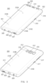
- FIG. 3 is a perspective view illustrating a front surface and a rear surface of an electronic device according to an embodiment of the disclosure.
- an electronic device 300 may include a housing 310 including a first surface (or front surface) 310A, a second surface (or rear surface) 310B, and a side surface 310C surrounding a space between the first surface 310A and the second surface 310B.
- the housing may refer to a structure forming portions of the first surface 310A, the second surface 3 10B, and the side surface 310C in FIG. 1 .
- the first surface 310A may be formed by a front plate 302 that is at least partially substantially transparent (e.g., a glass plate or a polymer plate including various coating layers).
- the second surface 310B may be formed by a substantially opaque rear plate 311.
- the rear plate 311 may be formed by, for example, coated or colored glass, ceramic, polymer, metal (e.g., aluminum, stainless steel (STS), or magnesium), or a combination of at least two of the above materials.
- the side surface 310C may be coupled to the front plate 302 and the rear plate 311, and may be formed by a side bezel structure (or "side member") 318 including metal and/or polymer.
- the rear plate 311 and the side bezel structure 318 may be integrally formed and may include the same material (e.g., metal material such as aluminum).
- the front plate 302 may include two first regions 310D extending seamlessly by being bent from the first surface 310A toward the rear plate 311 at both long edge ends of the front plate 302.
- the rear plate 311 may include two second regions 310E extending seamlessly by being bent from the second surface 310B toward the front plate 302 at both long edge ends of the rear plate 311.
- the front plate 302 (or the rear plate 311) may include one of the first regions 310D (or the second regions 310E). In another embodiment, some of the first regions 310D or the second regions 310E may not be included.
- the side bezel structure 318 when viewed from the side of the electronic device 300, may have a first thickness (or width) on the side where the first regions 310D or the second regions 310E are not disposed and may have a second thickness thinner than the first thickness on the side where the first regions 310D or the second regions 310E are disposed.
- the electronic device 300 may include at least one or more of a display 301, audio modules 303, 307, and 314, sensor modules 304, 316, and 319, camera modules 305, 312, and 313, a key input device 317, a light emitting device 306, and connector holes 308 and 309.
- at least one of the components e.g., the key input device 317 or the light emitting device 306 may be omitted or another component may be included.
- the display 301 may be exposed through, for example, a substantial portion of the front plate 302. In some embodiments, at least a portion of the display 301 may be exposed through the front plate 302 forming the first surface 310A and the first regions 310D of the side surface 310C. In some embodiments, the edges of the display 301 may be formed to be substantially the same in shape as outer edges of the front plate 302 adjacent thereto. In another embodiment (not shown), the distances between the outer edges of the display 301 and the outer edges of the front plate 302 may be formed substantially the same in order to expand an area where the display 301 is exposed.
- the screen display region of the display 301 may have a recess or opening in a portion thereof, and at least one or more of the audio module 314, the sensor module 304, the camera module 305, and the light emitting device 306 may be aligned with the recess or opening.
- at least one of the audio module 314, the sensor module 304, the camera module 305, the fingerprint sensor 316, and the light emitting device 306 may be located behind the screen display area of the display 301.
- the display 301 may be coupled or adjacent to a touch sensing circuit, a pressure sensor capable of measuring the strength (pressure) of a touch, and/or a digitizer for detecting a magnetic field-type stylus pen.
- a touch sensing circuit capable of measuring the strength (pressure) of a touch
- a digitizer for detecting a magnetic field-type stylus pen.
- at least a part of the sensor modules 304 and 319 and/or at least part of the key input device 317 may be disposed in the first regions 310D and/or the second regions 310E.
- the audio modules 303, 307, and 314 may include the microphone hole 303 and speaker holes 307 and 314.
- the microphone hole 303 may receive a microphone to obtain external sounds, and in some embodiments, a plurality of microphones to detect the direction of a sound.
- the speaker holes 307 and 314 may include the external speaker hole 307 and the phone receiver hole 314.
- the speaker holes 307 and 314 and the microphone hole 303 may be implemented as one hole, or a speaker may be included without the speaker holes 307 and 314 (e.g., piezo speaker).
- the sensor modules 304, 316, and 319 may generate an electrical signal or data value corresponding to an internal operating state or external environmental state of the electronic device 300.
- the sensor modules 304, 316, 319 may include the first sensor module 304 (e.g., a proximity sensor), a second sensor module (not shown) (e.g., a fingerprint sensor) disposed on the first surface 310A of the housing 310, the third sensor module 319 (e.g., a heart-rate monitor (HRM) sensor), and/or the fourth sensor module 316 (e.g., a fingerprint sensor) disposed on the second surface 310B of the housing 310.
- the first sensor module 304 e.g., a proximity sensor
- a second sensor module not shown
- the third sensor module 319 e.g., a heart-rate monitor (HRM) sensor
- the fourth sensor module 316 e.g., a fingerprint sensor
- the fingerprint sensor may be disposed on the first surface 310A (e.g., the display 301) as well as the second surface 310B of the housing 310.
- the electronic device 300 may further include a sensor module not illustrated, for example, at least one of a gesture sensor, a gyro sensor, an atmospheric pressure sensor, a magnetic sensor, an acceleration sensor, a grip sensor, a color sensor, an infrared (IR) sensor, a biometric sensor, a temperature sensor, a humidity sensor, or the illuminance sensor.
- a sensor module not illustrated, for example, at least one of a gesture sensor, a gyro sensor, an atmospheric pressure sensor, a magnetic sensor, an acceleration sensor, a grip sensor, a color sensor, an infrared (IR) sensor, a biometric sensor, a temperature sensor, a humidity sensor, or the illuminance sensor.
- the camera modules 305, 312, and 313 may include the first camera device 305 disposed on the first surface 310A of the electronic device 300, the second camera device 312 and/or the flash 313 disposed on the second surface 310B.
- the camera devices 305 and 312 may include one or more lenses, an image sensor, and/or an image signal processor.
- the flash 313 may include, for example, a light emitting diode or a xenon lamp.
- two or more lenses an infrared (IR) camera, a wide-angle lens, and a telescopic lens
- image sensors may be disposed on one surface of the electronic device 300.
- the key input device 317 may be disposed on the side surface 310C of the housing 310.
- the electronic device 101 may exclude all or some of the above-mentioned key input devices 317 and the excluded key input devices 317 may be implemented in other forms, such as soft keys, on the display 301.
- the key input device may include the sensor module 316 disposed on the second surface 310B of the housing 310.
- the light emitting device 306 may be disposed, for example, on the first surface 310A of the housing 310.
- the light emitting device 306 may provide, for example, state information of the electronic device 300 in the form of light.
- the light emitting device 306 may provide a light source that interacts with the camera module 305, for example.
- the light emitting device 306 may include, for example, an LED, an IR LED, and a xenon lamp.
- the connector holes 308 and 309 may include the first connector hole 308 for receiving a connector for transmitting or receiving power and/or data to/from an external electronic device and/or the second connector hole 309 (e.g., an earphone jack) for receiving a connector for transmitting or receiving audio signals to/from the external electronic device.
- the second connector hole 309 e.g., an earphone jack
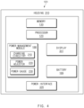
- FIG. 4 is a block diagram of an electronic device according to an embodiment of the disclosure.
- the electronic device 101 may include the housing 310, a power interface 320, the processor 120, the memory 130, the power management module 188, the battery 189, and the display 301 (e.g., the display device 160 of FIG. 1 ).
- the housing 310 may form outer edges of the electronic device 101.
- the housing 310 may include a front plate (e.g., the front plate 302 of FIG. 3 ) forming a front surface (or the first surface) of the electronic device 101, a rear plate forming a rear surface (or a second surface) of the electronic device 101, and a side member (e.g., the side member 318 of FIG. 3 ) surrounding a space between the front and rear plates.
- the housing 310 may protect the power interface 320, the processor 120, the memory 130, the power management module 188, the battery 189, and the display 301 from an external shock.
- the power interface 320 may be exposed through at least a portion of the housing 310 to be connected to an external power source (e.g., a wired power source connected to a power adapter or a USB) in a wired manner, or may be disposed inside the housing 310 to be connected to an external power source (a wireless power source) in a wireless manner.
- the power interface 320 may include at least one, for example, a USB connector (e.g., the connecting terminal 178 of FIG. 1 ), a physical medium such as a power receiving coil (e.g., the antenna module 197 of FIG. 1 ), or a USB interface supporting a protocol (e.g., the interface 177 of FIG. 1 ).
- the processor 120 located inside the housing 310 may be operatively connected to the power interface 320, the power management module 188, the battery 189, and the display 301.
- the processor 120 may monitor a time (e.g., a connection holding time) during which the external power source is connected to the power interface 320.
- the processor 120 may obtain usage state information of the battery 189 (e.g., the capacity, the number of charge/discharge cycles, the voltage or the temperature of the battery 189) through the charging circuitry 210 and the power gauge 230 of the power management module 188.
- the processor 120 may monitor a connection holding time between the power interface 320 and the external power source from a time point at which the voltage of the battery 189 reaches the first voltage value. For example, the processor 120 may determine whether the connection holding time has elapsed longer than a first time. For example, the processor 120 may lower the voltage of the battery 189 to a second voltage value lower than the first voltage value by discharging the battery 189 through the power management module 188.
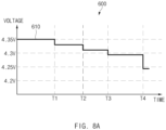
- the processor 120 may determine whether the voltage of the battery 189 reaches a voltage value corresponding to a fully-charged state in a state in which the external power source is connected to the power interface 320. For example, the processor 120 may monitor a connection holding time from a time point at which the voltage of the battery 189 reaches the voltage value (e.g., a first voltage value) corresponding to the fully-charged state in a state in which the external power source is connected to the power interface 320. The processor 120 may determine whether the connection holding time has elapsed longer than section-wise threshold times. The processor 120 may lower the voltage value corresponding to the fully-charged state according to set values when the connection holding time elapses longer than the section-wise threshold times.
- the processor 120 may monitor a connection holding time from a time point at which the voltage of the battery 189 reaches the voltage value (e.g., a first voltage value) corresponding to the fully-charged state in a state in which the external power source is connected to the power interface 320.
- the voltage value corresponding to the fully-charged state may correspond to, for example, a set value that is lowered in a stepwise manner whenever the connection holding time elapses longer than section-wise threshold times.
- the section-wise threshold times may be set for each time point at which a predetermined section ends (or starts) while a time is accumulated from the start of the connection holding time.
- the processor 120 may determine whether a voltage of the battery 189 corresponds to the voltage value at the fully-charged state when the connection holding time elapses longer than at least one of the section-wise threshold times. When the connection holding time elapses longer than a first threshold time, the processor 120 may lower the voltage value corresponding to the fully-charged state according to the set values when the voltage of the battery 189 is greater than the voltage value at the fully-charged state (for example, 4.33 V).
- the processor 120 may block an external power supplied from the power management module 188 to the battery 189 and an external power supplied from the power management module 188 to the display 301 whenever the connection holding time elapses longer than the section-wise threshold times.
- the processor 120 may control the power management module 188 such that a discharge current is supplied to the display 301 or the processor 120 through the battery 189 as a driving current.
- the processor 120 may control the power management module 188 such that a discharge current is supplied through the battery 189 as a driving current for at least one of components (e.g., Wi-Fi, CP, AP, BT, or LED) of the electronic device.
- components e.g., Wi-Fi, CP, AP, BT, or LED
- the processor 120 may determine whether the voltage of the battery 189 reaches a set value one-level lower than a voltage value corresponding to a fully-charged state of one of the section-wise threshold times. When the voltage of the battery 189 reaches the set value one-level lower than the voltage value corresponding to the fully-charged state of any one threshold time, the processor 120 may control the power management module 188 such that an external power supplied to the battery 189 is maintained to be blocked. In addition, when the voltage of the battery 189 reaches the set value one-level lower than the voltage value corresponding to the fully-charged state of any one threshold time, the processor 120 may control the power management module 188 such that an external power is supplied to the display 301 or the processor 120.
- the processor 120 may continue to accumulate the connection holding time even when the external power source is not connected through the power interface 320. For example, when the external power source is disconnected from the power interface 320, and is then reconnected through the power interface 320 within a set time (e.g., 2 hours), the processor 120 may continuously accumulate the connection holding time. For example, when the external power source is disconnected from the power interface 320, and is then reconnected through the power interface 320 in a state in which the voltage of the battery 189 is not lowered below a set voltage (e.g., 4.15 V), the processor 120 may continuously accumulate the connection holding time.
- a set voltage e.g., 4.15 V
- the processor 120 may continuously accumulate the connection holding time.
- stage-wise set values at fully-charged states according to the section-wise threshold times may be given as the example of Table 1.
- Table 1 shows stage-wise set values and stage-wise charge-triggering voltage values at fully-charged states according to the section-wise threshold times.
- Table 1 Threshold time Set value at fully-charged state(V) Charge-triggering voltage value(V) 4.35 4.28 T1 4.33 4.26 T2 4.31 4.24 T3 4.29 4.22 T4 4.24 4.17
- the processor 120 may determine whether the connection holding time has elapsed longer than threshold times. The processor 120 may lower the voltage value corresponding to the fully-charged state according to the set values when the connection holding time elapses longer than the threshold times. For example, when the connection holding time elapses longer than a first threshold time (e.g., T1) after the voltage of the battery 189 reaches a voltage value (e.g., 4.35 V) corresponding to a first fully-charged state, the processor 120 may lower the voltage value corresponding to the first fully-charged state to a first set value (e.g., 4.33 V).
- a first threshold time e.g., T1
- a voltage value e.g., 4.35 V
- the processor 120 may maintain a voltage value corresponding to the fully-charged state to be maintained at the lowest stage or to be restored to a set value at the highest stage (e.g., 4.35 V) whether the power interface 320 is connected to an external power source.
- a set value e.g., 4.24 V
- the charge-triggering voltage value representing that the voltage of the battery 189 is the minimum voltage value at which charging is able to be started may be lowered from a first charge-triggering voltage value (4.28 V) to a fourth charge-triggering voltage value (e.g., 4.17 V) in proportional to the voltage value at the fully-charged state, which is lowered according to the set values.
- the threshold times (e.g., T1 to T4) in Table 1 may be converted into cumulative numbers of times by counting a set time (e.g., 172.8 seconds) as one time.
- a first threshold time T1 may represent a result of accumulation of the set time (e.g., 172.8) by a set number of times (e.g., 300 times).
- a second threshold time T2 may represent a result of accumulation of the set time (e.g., 172.8) by a set number of times (e.g., 400 times).
- a third threshold time T3 may represent a result of accumulation of the set time (e.g., 172.8) by a set number of times (e.g., 700 times).
- a fourth threshold time T4 may represent a result of accumulation of the set time (e.g., 172.8) by a set number of times (e.g., 1000 times).
- the memory 130 disposed inside the housing 310 may be operatively connected to the processor 120.
- the memory 130 may store a variety of data (e.g., instructions) used by the processor 120.
- the variety of data stored in the memory 130 may be transferred to the processor 120 at, for example, a request of the processor 120, or may be extracted by access of the processor 120 and executed in the processor 120.
- the power management module 188 may include the charging circuitry 210, the power adjuster 220, and the power gauge 230.
- the power management module 188 may be implemented with, for example, a power management integrated circuit (PMIC).
- PMIC power management integrated circuit
- the power management module 188 may control charging and discharging of the battery 189 according to a command of the processor 120.
- the power management module 188 may supply external power supplied through the power interface 320 to the battery 189 according to a command of the processor 120.
- the power management module 188 may switch the battery 189 to a discharge state by blocking an external power supplied to at least one of the components of the electronic device 101 (e.g., the display 301), and supplying a power from the battery 189 to at least one of the components of the electronic device 101, according to a command of the processor 120.
- the power management module 188 may release the discharge state of the battery 189 by supplying an external power to at least one of the components of the electronic device 101 in a state in which the external power supplied to the battery 189 is blocked, according to a command of the processor 120.
- At least one battery 189 disposed inside the housing 310 may be electrically connected to the power interface 320 through the power management module 188.
- the battery 189 may be charged by an external power supplied from the power management module 188.
- an external power supplied to the battery 189 from the power management module 188 may be blocked.
- a discharge current may be generated to enable the voltage of the battery 189 to reach a set value one-level lower than a voltage value corresponding to a fully-charged state of one of the section-wise threshold times.
- the discharge current generated according to the discharge state of the battery 189 may be used as a driving current of at least one of the components of the electronic device.
- the discharge current may not be generated in the battery 189 by releasing the discharge state while the external power from the power management module 188 is being blocked.
- the display 301 may be electrically connected to the power management module 188 and the battery 189.
- the display 301 may be operated by an external power supplied from the power management module 188 or a discharge current supplied from the battery 189.
- the display 301 may provide visual information to the outside (e.g., a user) of the electronic device 101.
- the external power supplied from the power management module 188 may be blocked in the display 301.
- the display 301 may be operated by the discharge current supplied from the battery 189 instead of the external power supplied from the power management module 188.
- the discharge current supplied from the battery 189 to the display 301 may be blocked when the voltage of the battery 189 reaches a set value at a desired stage (e.g., stage-wise set values at fully-charged states in Table 1).
- the display 301 may be operated by an external power supplied from the power management module 188 again.
- the display 301 may display a battery level of a predetermined level (e.g., 100%) through a user interface, whenever the section-wise threshold times elapse, although the voltage of the battery 189 is gradually lowered according to stage-wise set values at a fully-charged state corresponding to the section-wise threshold times. For example, although the connection holding time elapses longer than a first threshold time and the voltage of the battery 189 is lowered to a second set value (e.g., 4.33 V) corresponding to a second fully-charged state from a first set value (e.g., 4.35 V) corresponding to a first fully-charged state, the display 301 may display a battery level of 100% through the user interface.
- a predetermined level e.g., 100%
- FIG. 5 is a circuit diagram of an electronic device according to an embodiment of the disclosure.
- the electronic device 101 may supply an external power VBUS supplied through a power interface (e.g., the power interface 320 of FIG. 4 ) for a system power VSYS and/or a battery voltage VBAT through the power management module 188 (e.g., PMIC).
- the system power VSYS may include, for example, a current for driving at least one of the components of the electronic device 101 (e.g., the display 301 of FIG. 4 ).
- the power management module 188 may include a buck converter 188_1 (e.g., the power adjuster 220 of FIG. 4 ) and a switching element 188_2.
- the buck converter 188_1 may be set to an ON state or an OFF state under the control of a processor (e.g., the processor 120 of FIG. 4 ).
- the switching element 188_2 may be set to an ON state opposite to the OFF state of the buck converter 188_1.
- the switching element 188_2 may be set to an OFF state opposite to the ON state of the buck converter 188 1.
- the buck converter 188_1 may be set to the OFF state under the control of the processor, and thus the external power VBUS supplied for the system power VSYS and the battery voltage VBAT may be blocked.
- the switching element 188_2 may be set to the ON state.
- the battery voltage VBAT may be switched to the discharge state, and a discharge current may be generated.
- the discharge current of the battery voltage VBAT may be supplied to the system power VSYS (e.g., the display 301 of FIG. 4 ).
- the buck converter 188_1 may be set to the ON state under the control of the processor, so that the external power VBUS may be supplied to the system power VSYS.
- the switching element 188_2 may be set to the OFF state.
- the discharge state of the battery voltage VBAT may be released.
- FIG. 6 is a flowchart of a method of controlling charging of an electronic device according to an embodiment of the disclosure.
- the processor 120 determines whether the voltage of the battery 189 reaches the first voltage value corresponding to a fully-charged state. In operation 410, when the voltage of the battery 189 reaches the first voltage value (410 -Yes), the processor 120 performs operation 420. In operation 410, when the voltage of the battery 189 does not reach the first voltage value (410 -No), the processor 120 performs operation 410 repeatedly.
- the processor 120 may determine whether a connection holding time has elapsed longer than a first time. In operation 420, the processor 120 may perform operation 430 when the connection holding time has elapsed longer than the first time (420-Yes). In operation 420, the processor 120 may repeatedly perform operation 420 when the connection holding time has not elapsed longer than the first time (420 -No).
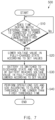
- FIG. 7 is a flowchart of a method of controlling charging of an electronic device according to an embodiment of the disclosure.
- the processor 120 of an electronic device monitors 500 a connection holding time between the power interface 320 and the external power source after the voltage of the battery 189 reaches a voltage value corresponding to a fully-charged state.
- the processor 120 changes a voltage value corresponding to a fully-charged state to set values at stage-wise fully-charged states when the connection holding time elapses longer than section-wise threshold times.
- the processor 120 determines whether the connection holding time has elapsed longer than a first threshold time. For example, the processor 120 may measure the connection holding time after the voltage of the battery 189 reaches a voltage value corresponding to a first fully-charged state in a state in which the external power is connected to the power interface 320. In operation 510, the processor 120 may perform operation 520 when the connection holding time has elapsed longer than the first threshold time (510 -Yes). In operation 510, the processor 120 may repeatedly perform operation 510 when the connection holding time have not elapsed longer than the first threshold time (510 -No).
- the processor 120 whenever section-wise threshold times elapses sequentially, the processor 120 lowers a voltage value corresponding to the fully-charged state in a stepwise manner according to set values.
- the processor 120 controls the power management module 188 such that the battery 189 is switched to a discharge state whenever the voltage of the battery 189 corresponds to set values at the stage-wise fully-charged states.
- the processor 120 allows the discharge state of the battery 189 to be released according to whether the voltage of the battery 189 reaches a voltage value of a fully-charged state, which is lowered according to the set values, according to a discharge state.
- the third charge-triggering voltage value for example, 4.24 V
- the third fully-charged state may be lowered to a fourth charge-triggering voltage value (e.g., 4.22 V) which is one-level lower than the third charge-triggering voltage value (e.g., 4.24 V).
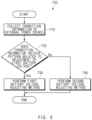
- the processor 120 may perform a first battery voltage adjusting method used in the electronic device 101 for a personal purpose.
- the processor 120 may change a voltage value and a charge-triggering voltage value which correspond to the fully-charged state of the battery 189, according to the first battery voltage adjusting method.
- the processor 120 may allow a voltage value corresponding to the fully-charged state to be lowered in a stepwise manner according to a set value whenever the connection holding time elapses longer than threshold times for each section by performing the first battery voltage adjusting method.
- the processor 120 may allow a charge-triggering voltage value to be lowered in a stepwise manner according to a change in a voltage value corresponding to the fully-charged state whenever the connection holding time elapses longer than threshold times for each section by performing the second battery voltage adjusting method.
- the electronic device may further include a power management integrated circuit (PMIC) (e.g., the power management module 188 of FIG. 4 ).
- PMIC power management integrated circuit
- the instructions may cause the processor to supply the external power to the display or the processor through the PMIC.
- the method may further include allowing the power management module to supply the external power to the display or the processor when the discharge state is released.
- the method may further include continuously accumulating the connection holding time when the power interface is separated from the external power source and is then connected to the external power source within a set time.
- the method may further include continuously accumulating the connection holding time when the power interface is separated from the external power source and is then connected to the external power source in a state in which a voltage level of the battery is not lowered below a set level.
- a method may be included and provided in a computer program product.
- the computer program product may be traded as a product between a seller and a buyer.
- the computer program product may be distributed in the form of a machine-readable storage medium (e.g., compact disc read only memory (CD-ROM)), or be distributed (e.g., downloaded or uploaded) online via an application store (e.g., PlayStore TM ), or between two user devices (e.g., smart phones) directly. If distributed online, at least part of the computer program product may be temporarily generated or at least temporarily stored in the machine-readable storage medium, such as memory of the manufacturer's server, a server of the application store, or a relay server.
- CD-ROM compact disc read only memory
- an application store e.g., PlayStore TM
- two user devices e.g., smart phones
Landscapes
- Engineering & Computer Science (AREA)
- Power Engineering (AREA)
- Theoretical Computer Science (AREA)
- Physics & Mathematics (AREA)
- General Engineering & Computer Science (AREA)
- General Physics & Mathematics (AREA)
- Charge And Discharge Circuits For Batteries Or The Like (AREA)
- Control Of Charge By Means Of Generators (AREA)
Claims (9)
- Dispositif électronique (101) comprenant :un logement ;une interface de puissance (320) configurée pour être connectée à une source d'alimentation externe à travers le logement ;un module de gestion de puissance (188) connecté électriquement à l'interface de puissance ;au moins une batterie (189) configurée pour être chargée par une alimentation externe fournie à travers le module de gestion de puissance (188) ;un processeur (120) connecté de manière opérationnelle à l'interface de puissance (320) ; etune mémoire (130) configurée pour stocker des instructions,où, lorsque les instructions sont exécutées, le processeur (120) est configuré pour :abaisser activement une valeur de tension de l'au moins une batterie selon des valeurs définies de manière progressive en réponse à un temps de maintien de connexion entre l'interface de puissance (320) et la source d'alimentation externe dépassant des temps seuil par section après qu'une tension de l'au moins une batterie a atteint la valeur de tension dans un état dans lequel la source d'alimentation externe est connectée à l'interface de puissance (320) ; etcommander au module de gestion de puissance (188) de bloquer l'alimentation externe fournie à l'au moins une batterie (189) lorsque la tension de l'au moins une batterie (189) est supérieure ou égale à la valeur de tension,où à la valeur de tension, l'au moins une batterie (189) est considérée comme étant complètement chargée de sorte que l'au moins une batterie n'est plus chargée,
etoù le processeur (120) est en outre configuré pour :lors de l'abaissement de la valeur de tension de l'au moins une batterie aux valeurs définies de manière progressive, commander au module de gestion de puissance de commuter l'au moins une batterie à un état de décharge ; etcommander au module de gestion de puissance (188) de libérer l'état de décharge de l'au moins une batterie lorsque la tension de l'au moins une batterie a atteint la valeur de tension, qui est abaissée selon les valeurs définies. - Dispositif électronique (101) selon la revendication 1, comprenant en outre :un écran (301) configuré pour être actionné par au moins l'un entre l'alimentation externe fournie à travers le module de gestion de puissance et un courant de décharge fourni par l'au moins une batterie,où, lorsque les instructions sont exécutées, le processeur (120) est en outre configuré pour commander au module de gestion de puissance de bloquer l'alimentation externe fournie à l'écran ou au processeur.
- Dispositif électronique (101) selon la revendication 1, où, lorsque les instructions sont exécutées, le processeur (120) est en outre configuré pour commander au module de gestion de puissance (188) de fournir l'alimentation externe à un écran ou au processeur dans un état dans lequel l'alimentation externe fournie à l'au moins une batterie est bloquée lorsque l'état de décharge est libéré.
- Procédé de commande de charge d'une batterie, le procédé comprenant :déterminer si un temps de maintien de connexion d'une connexion entre une interface de puissance et une source d'alimentation externe a dépassé les temps seuil par section après qu'une tension de la batterie a atteint une valeur de tension dans un état dans lequel la source d'alimentation externe est connectée à l'interface de puissance ;abaisser activement la valeur de tension selon des valeurs définies de manière progressive chaque fois que le temps de maintien de connexion dépasse des temps seuil par section ; etcommander au module de gestion de puissance de bloquer l'alimentation externe fournie à la batterie lorsque la tension de la batterie est supérieure ou égale à la valeur de tension,où à la valeur de tension, la batterie est considérée comme complètement chargée de sorte que la batterie n'est plus chargée, etoù le procédé comprend en outre :lors de l'abaissement de la valeur de tension de la batterie aux valeurs définies de manière progressive, commander au module de gestion de puissance de commuter la batterie à un état de décharge ; etcommander au module de gestion de puissance de libérer l'état de décharge de la batterie lorsque la tension de la batterie a atteint la valeur de tension, qui est abaissée selon les valeurs définies.
- Procédé selon la revendication 4, comprenant en outre :
commander au module de gestion de puissance de commuter la batterie à l'état de décharge dans un état dans lequel la batterie est connectée à un écran ou à un processeur. - Procédé selon la revendication 5, comprenant en outre :
commander au module de gestion de puissance de fournir une alimentation externe à l'écran ou au processeur lorsque l'état de décharge est libéré. - Procédé selon la revendication 4, comprenant en outre :
accumuler en continu le temps de maintien de connexion lorsque l'interface de puissance est séparée de la source d'alimentation externe et est ensuite connectée à la source d'alimentation externe dans un temps défini. - Procédé selon la revendication 4, comprenant en outre :
accumuler en continu le temps de maintien de connexion lorsque l'interface de puissance est séparée de la source d'alimentation externe et est ensuite connectée à la source d'alimentation externe dans un état dans lequel la tension de la batterie n'est pas abaissée en dessous d'un tension définie. - Procédé selon la revendication 4, comprenant en outre :
accumuler en continu le temps de maintien de connexion lorsque l'interface de puissance est séparée de la source d'alimentation externe et est ensuite connectée à la source d'alimentation externe dans un état dans lequel un niveau de tension de la batterie n'est pas abaissée en dessous d'un niveau défini.
Applications Claiming Priority (1)
| Application Number | Priority Date | Filing Date | Title |
|---|---|---|---|
| KR1020190023937A KR102710751B1 (ko) | 2019-02-28 | 2019-02-28 | 배터리의 충전을 제어하는 방법 및 그 방법을 적용한 전자 장치 |
Publications (2)
| Publication Number | Publication Date |
|---|---|
| EP3702885A1 EP3702885A1 (fr) | 2020-09-02 |
| EP3702885B1 true EP3702885B1 (fr) | 2023-09-27 |
Family
ID=69784051
Family Applications (1)
| Application Number | Title | Priority Date | Filing Date |
|---|---|---|---|
| EP20158411.7A Active EP3702885B1 (fr) | 2019-02-28 | 2020-02-20 | Procédé de commande de chargement de batterie et dispositif électronique sur lequel ce procédé est appliqué |
Country Status (4)
| Country | Link |
|---|---|
| US (1) | US11495986B2 (fr) |
| EP (1) | EP3702885B1 (fr) |
| KR (1) | KR102710751B1 (fr) |
| WO (1) | WO2020175798A1 (fr) |
Families Citing this family (4)
| Publication number | Priority date | Publication date | Assignee | Title |
|---|---|---|---|---|
| CN110911770B (zh) * | 2019-11-26 | 2023-06-27 | Oppo广东移动通信有限公司 | 充电方法及待充电设备 |
| CN112686360A (zh) * | 2020-12-25 | 2021-04-20 | 北京中建京诚自动化技术有限公司 | 一种用于移动式皮带机装车发货的计数器及皮带机 |
| EP4340167A4 (fr) * | 2021-08-11 | 2024-12-25 | Samsung Electronics Co., Ltd. | Dispositif électronique et procédé de charge l'utilisant |
| US12413086B2 (en) * | 2022-04-26 | 2025-09-09 | Dell Products L.P. | Adjusting a charging rate of a battery of an information handling system |
Citations (1)
| Publication number | Priority date | Publication date | Assignee | Title |
|---|---|---|---|---|
| JP2011109840A (ja) * | 2009-11-19 | 2011-06-02 | Lenovo Singapore Pte Ltd | 二次電池の寿命期間を保証する充電システム |
Family Cites Families (21)
| Publication number | Priority date | Publication date | Assignee | Title |
|---|---|---|---|---|
| US5545969A (en) * | 1992-12-02 | 1996-08-13 | Matsushita Electric Industrial Co., Ltd. | Battery residual capacity displaying system with discharged electrical quantity computation section |
| JP2929921B2 (ja) * | 1993-12-21 | 1999-08-03 | 三菱電機株式会社 | 電子機器及び電池管理装置及び電池管理方法 |
| JP2780699B2 (ja) * | 1996-04-11 | 1998-07-30 | 日本電気株式会社 | パーソナルコンピュータのバッテリ制御方法と電源制御回路 |
| JP3721690B2 (ja) * | 1997-02-10 | 2005-11-30 | 日産自動車株式会社 | 2次電池の保護装置 |
| JP3775131B2 (ja) * | 1999-09-27 | 2006-05-17 | 松下電工株式会社 | 充電装置 |
| EP1128517A3 (fr) * | 2000-02-24 | 2003-12-10 | Makita Corporation | Adaptateur pour blocs de batteries secondaires |
| JP2001309568A (ja) | 2000-04-26 | 2001-11-02 | Internatl Business Mach Corp <Ibm> | 充電システム、充電制御装置、充電制御方法及びコンピュータ |
| JP4093205B2 (ja) | 2003-12-05 | 2008-06-04 | 松下電器産業株式会社 | 充電制御装置 |
| US7612536B2 (en) | 2005-10-17 | 2009-11-03 | Hewlett-Packard Development Company, L.P. | Pre-set discharging of batteries |
| KR100991084B1 (ko) | 2005-12-15 | 2010-10-29 | 주식회사 엘지화학 | 멀티 전지 팩 시스템 및 그 제어방법, 및 이를 이용한 전지팩 |
| JP2008035674A (ja) * | 2006-07-31 | 2008-02-14 | Mitsumi Electric Co Ltd | 充電用電源装置 |
| CN101611524B (zh) * | 2007-01-25 | 2013-12-11 | 永备电池有限公司 | 便携式电源供应 |
| KR20100046562A (ko) | 2008-10-27 | 2010-05-07 | 삼성전자주식회사 | 휴대 단말기의 충전 제어 방법 및 충전 제어 장치 |
| CN103155347B (zh) * | 2010-12-13 | 2015-06-24 | 三洋电机株式会社 | 充电设备、电力存储设备以及电源设备 |
| TW201407179A (zh) | 2012-08-12 | 2014-02-16 | 仁寶電腦工業股份有限公司 | 電子裝置及其偵測電池變形的方法 |
| EP3567712B1 (fr) | 2014-09-02 | 2020-11-25 | Apple Inc. | Chargement de batterie multi-phases avec dérivation de suralimentation |
| KR102336856B1 (ko) | 2014-11-13 | 2021-12-08 | 삼성전자 주식회사 | 전자 장치 및 그의 배터리 충방전 제어 방법 |
| US10158149B2 (en) | 2014-11-20 | 2018-12-18 | Motorola Solutions, Inc. | Method and apparatus to detect and manage battery pack cell swell |
| EP3905479B1 (fr) * | 2016-11-14 | 2025-05-07 | SZ DJI Technology Co., Ltd. | Système multi-batterie et gestion associée |
| JP6490148B2 (ja) * | 2017-06-12 | 2019-03-27 | 本田技研工業株式会社 | 充電制御装置 |
| CN107666167A (zh) * | 2017-11-21 | 2018-02-06 | 深圳市森树强电子科技有限公司 | 一种新型三段式充电管理方法及装置 |
-
2019
- 2019-02-28 KR KR1020190023937A patent/KR102710751B1/ko active Active
-
2020
- 2020-01-16 WO PCT/KR2020/000764 patent/WO2020175798A1/fr not_active Ceased
- 2020-01-28 US US16/774,203 patent/US11495986B2/en active Active
- 2020-02-20 EP EP20158411.7A patent/EP3702885B1/fr active Active
Patent Citations (1)
| Publication number | Priority date | Publication date | Assignee | Title |
|---|---|---|---|---|
| JP2011109840A (ja) * | 2009-11-19 | 2011-06-02 | Lenovo Singapore Pte Ltd | 二次電池の寿命期間を保証する充電システム |
Also Published As
| Publication number | Publication date |
|---|---|
| KR20200105162A (ko) | 2020-09-07 |
| KR102710751B1 (ko) | 2024-09-27 |
| US11495986B2 (en) | 2022-11-08 |
| US20200280205A1 (en) | 2020-09-03 |
| EP3702885A1 (fr) | 2020-09-02 |
| WO2020175798A1 (fr) | 2020-09-03 |
Similar Documents
| Publication | Publication Date | Title |
|---|---|---|
| EP3922042B1 (fr) | Dispositif électronique d'alimentation et procédé de commande de ce dispositif électronique | |
| KR102767967B1 (ko) | 복수의 배터리들의 충전을 제어하는 방법 및 그 방법을 적용한 전자 장치 | |
| US11288407B2 (en) | Method and electronic device for controlling voltage output to external electronic device according to size of voltage detected at signal terminal connected to external electronic device | |
| US11489212B2 (en) | Method of controlling plurality of batteries and electronic device to which the same is applied | |
| US11437839B2 (en) | Method of controlling charging of plurality of batteries and electronic device to which the method is applied | |
| EP3518380B1 (fr) | Dispositif électronique incluant une batterie et son procédé de commande de charge | |
| KR102610543B1 (ko) | 전자 장치 및 그의 배터리를 진단하는 방법 | |
| US11495986B2 (en) | Method of controlling charging of battery and electronic device to which the method is applied | |
| KR102800823B1 (ko) | 배터리를 충전하는 방법 및 상기 배터리를 포함하는 전자 장치 | |
| CN113383479B (zh) | 用于对外部装置无线充电的电子装置 | |
| US11509156B2 (en) | Apparatus and method for charging battery | |
| EP3771987B1 (fr) | Dispositif électronique pour prévenir les dommages de dispositif usb et son procédé de fonctionnement | |
| KR20200048975A (ko) | 복수의 부분들의 배터리를 충전하는 전자 장치 | |
| KR20210078224A (ko) | 배터리의 수명을 관리하기 위한 전자 장치 및 방법 | |
| KR20200042376A (ko) | 전자 장치 및 전자 장치에서 유무선 충전 방법 | |
| KR102751034B1 (ko) | 금속 물질을 탐지하는 전력 송신 장치 및 방법 | |
| KR102627633B1 (ko) | 커넥터의 연결 상태를 판단하기 위한 로직 회로를 포함하는 전자 장치 | |
| KR102809993B1 (ko) | 무선 충전 방법 및 이를 지원하는 전자 장치 | |
| KR102813607B1 (ko) | 무선 충전 방법 및 이를 지원하는 전자 장치 | |
| KR102800822B1 (ko) | 배터리를 충전하는 방법 및 그 방법을 적용한 전자 장치 | |
| KR102651536B1 (ko) | 전자 장치의 배터리 충전 제어 방법 및 그 전자 장치 | |
| US20230051147A1 (en) | Electronic device and method for charging thereof | |
| CN111585317A (zh) | 用于对外部电子装置进行无线充电的电子装置 | |
| KR20210101689A (ko) | 전자 장치 및 전자 장치의 센서 운용 방법 |
Legal Events
| Date | Code | Title | Description |
|---|---|---|---|
| PUAI | Public reference made under article 153(3) epc to a published international application that has entered the european phase |
Free format text: ORIGINAL CODE: 0009012 |
|
| STAA | Information on the status of an ep patent application or granted ep patent |
Free format text: STATUS: THE APPLICATION HAS BEEN PUBLISHED |
|
| AK | Designated contracting states |
Kind code of ref document: A1 Designated state(s): AL AT BE BG CH CY CZ DE DK EE ES FI FR GB GR HR HU IE IS IT LI LT LU LV MC MK MT NL NO PL PT RO RS SE SI SK SM TR |
|
| AX | Request for extension of the european patent |
Extension state: BA ME |
|
| STAA | Information on the status of an ep patent application or granted ep patent |
Free format text: STATUS: REQUEST FOR EXAMINATION WAS MADE |
|
| 17P | Request for examination filed |
Effective date: 20201119 |
|
| RBV | Designated contracting states (corrected) |
Designated state(s): AL AT BE BG CH CY CZ DE DK EE ES FI FR GB GR HR HU IE IS IT LI LT LU LV MC MK MT NL NO PL PT RO RS SE SI SK SM TR |
|
| STAA | Information on the status of an ep patent application or granted ep patent |
Free format text: STATUS: EXAMINATION IS IN PROGRESS |
|
| 17Q | First examination report despatched |
Effective date: 20220111 |
|
| GRAP | Despatch of communication of intention to grant a patent |
Free format text: ORIGINAL CODE: EPIDOSNIGR1 |
|
| STAA | Information on the status of an ep patent application or granted ep patent |
Free format text: STATUS: GRANT OF PATENT IS INTENDED |
|
| INTG | Intention to grant announced |
Effective date: 20230509 |
|
| RIN1 | Information on inventor provided before grant (corrected) |
Inventor name: HA, JAEMU Inventor name: LEE, JONGKYU Inventor name: KWON, HYUNGJUN Inventor name: KIM, BYUNGWOOK |
|
| GRAS | Grant fee paid |
Free format text: ORIGINAL CODE: EPIDOSNIGR3 |
|
| GRAA | (expected) grant |
Free format text: ORIGINAL CODE: 0009210 |
|
| STAA | Information on the status of an ep patent application or granted ep patent |
Free format text: STATUS: THE PATENT HAS BEEN GRANTED |
|
| AK | Designated contracting states |
Kind code of ref document: B1 Designated state(s): AL AT BE BG CH CY CZ DE DK EE ES FI FR GB GR HR HU IE IS IT LI LT LU LV MC MK MT NL NO PL PT RO RS SE SI SK SM TR |
|
| REG | Reference to a national code |
Ref country code: GB Ref legal event code: FG4D |
|
| REG | Reference to a national code |
Ref country code: CH Ref legal event code: EP |
|
| REG | Reference to a national code |
Ref country code: DE Ref legal event code: R096 Ref document number: 602020018119 Country of ref document: DE |
|
| REG | Reference to a national code |
Ref country code: IE Ref legal event code: FG4D |
|
| REG | Reference to a national code |
Ref country code: LT Ref legal event code: MG9D |
|
| PG25 | Lapsed in a contracting state [announced via postgrant information from national office to epo] |
Ref country code: GR Free format text: LAPSE BECAUSE OF FAILURE TO SUBMIT A TRANSLATION OF THE DESCRIPTION OR TO PAY THE FEE WITHIN THE PRESCRIBED TIME-LIMIT Effective date: 20231228 |
|
| PG25 | Lapsed in a contracting state [announced via postgrant information from national office to epo] |
Ref country code: SE Free format text: LAPSE BECAUSE OF FAILURE TO SUBMIT A TRANSLATION OF THE DESCRIPTION OR TO PAY THE FEE WITHIN THE PRESCRIBED TIME-LIMIT Effective date: 20230927 Ref country code: RS Free format text: LAPSE BECAUSE OF FAILURE TO SUBMIT A TRANSLATION OF THE DESCRIPTION OR TO PAY THE FEE WITHIN THE PRESCRIBED TIME-LIMIT Effective date: 20230927 Ref country code: NO Free format text: LAPSE BECAUSE OF FAILURE TO SUBMIT A TRANSLATION OF THE DESCRIPTION OR TO PAY THE FEE WITHIN THE PRESCRIBED TIME-LIMIT Effective date: 20231227 Ref country code: LV Free format text: LAPSE BECAUSE OF FAILURE TO SUBMIT A TRANSLATION OF THE DESCRIPTION OR TO PAY THE FEE WITHIN THE PRESCRIBED TIME-LIMIT Effective date: 20230927 Ref country code: LT Free format text: LAPSE BECAUSE OF FAILURE TO SUBMIT A TRANSLATION OF THE DESCRIPTION OR TO PAY THE FEE WITHIN THE PRESCRIBED TIME-LIMIT Effective date: 20230927 Ref country code: HR Free format text: LAPSE BECAUSE OF FAILURE TO SUBMIT A TRANSLATION OF THE DESCRIPTION OR TO PAY THE FEE WITHIN THE PRESCRIBED TIME-LIMIT Effective date: 20230927 Ref country code: GR Free format text: LAPSE BECAUSE OF FAILURE TO SUBMIT A TRANSLATION OF THE DESCRIPTION OR TO PAY THE FEE WITHIN THE PRESCRIBED TIME-LIMIT Effective date: 20231228 Ref country code: FI Free format text: LAPSE BECAUSE OF FAILURE TO SUBMIT A TRANSLATION OF THE DESCRIPTION OR TO PAY THE FEE WITHIN THE PRESCRIBED TIME-LIMIT Effective date: 20230927 |
|
| REG | Reference to a national code |
Ref country code: NL Ref legal event code: MP Effective date: 20230927 |
|
| REG | Reference to a national code |
Ref country code: AT Ref legal event code: MK05 Ref document number: 1616047 Country of ref document: AT Kind code of ref document: T Effective date: 20230927 |
|
| PG25 | Lapsed in a contracting state [announced via postgrant information from national office to epo] |
Ref country code: NL Free format text: LAPSE BECAUSE OF FAILURE TO SUBMIT A TRANSLATION OF THE DESCRIPTION OR TO PAY THE FEE WITHIN THE PRESCRIBED TIME-LIMIT Effective date: 20230927 |
|
| PG25 | Lapsed in a contracting state [announced via postgrant information from national office to epo] |
Ref country code: IS Free format text: LAPSE BECAUSE OF FAILURE TO SUBMIT A TRANSLATION OF THE DESCRIPTION OR TO PAY THE FEE WITHIN THE PRESCRIBED TIME-LIMIT Effective date: 20240127 |
|
| PG25 | Lapsed in a contracting state [announced via postgrant information from national office to epo] |
Ref country code: AT Free format text: LAPSE BECAUSE OF FAILURE TO SUBMIT A TRANSLATION OF THE DESCRIPTION OR TO PAY THE FEE WITHIN THE PRESCRIBED TIME-LIMIT Effective date: 20230927 |
|
| PG25 | Lapsed in a contracting state [announced via postgrant information from national office to epo] |
Ref country code: ES Free format text: LAPSE BECAUSE OF FAILURE TO SUBMIT A TRANSLATION OF THE DESCRIPTION OR TO PAY THE FEE WITHIN THE PRESCRIBED TIME-LIMIT Effective date: 20230927 |
|
| PG25 | Lapsed in a contracting state [announced via postgrant information from national office to epo] |
Ref country code: SM Free format text: LAPSE BECAUSE OF FAILURE TO SUBMIT A TRANSLATION OF THE DESCRIPTION OR TO PAY THE FEE WITHIN THE PRESCRIBED TIME-LIMIT Effective date: 20230927 Ref country code: RO Free format text: LAPSE BECAUSE OF FAILURE TO SUBMIT A TRANSLATION OF THE DESCRIPTION OR TO PAY THE FEE WITHIN THE PRESCRIBED TIME-LIMIT Effective date: 20230927 Ref country code: IS Free format text: LAPSE BECAUSE OF FAILURE TO SUBMIT A TRANSLATION OF THE DESCRIPTION OR TO PAY THE FEE WITHIN THE PRESCRIBED TIME-LIMIT Effective date: 20240127 Ref country code: ES Free format text: LAPSE BECAUSE OF FAILURE TO SUBMIT A TRANSLATION OF THE DESCRIPTION OR TO PAY THE FEE WITHIN THE PRESCRIBED TIME-LIMIT Effective date: 20230927 Ref country code: EE Free format text: LAPSE BECAUSE OF FAILURE TO SUBMIT A TRANSLATION OF THE DESCRIPTION OR TO PAY THE FEE WITHIN THE PRESCRIBED TIME-LIMIT Effective date: 20230927 Ref country code: CZ Free format text: LAPSE BECAUSE OF FAILURE TO SUBMIT A TRANSLATION OF THE DESCRIPTION OR TO PAY THE FEE WITHIN THE PRESCRIBED TIME-LIMIT Effective date: 20230927 Ref country code: AT Free format text: LAPSE BECAUSE OF FAILURE TO SUBMIT A TRANSLATION OF THE DESCRIPTION OR TO PAY THE FEE WITHIN THE PRESCRIBED TIME-LIMIT Effective date: 20230927 Ref country code: PT Free format text: LAPSE BECAUSE OF FAILURE TO SUBMIT A TRANSLATION OF THE DESCRIPTION OR TO PAY THE FEE WITHIN THE PRESCRIBED TIME-LIMIT Effective date: 20240129 Ref country code: SK Free format text: LAPSE BECAUSE OF FAILURE TO SUBMIT A TRANSLATION OF THE DESCRIPTION OR TO PAY THE FEE WITHIN THE PRESCRIBED TIME-LIMIT Effective date: 20230927 |
|
| PG25 | Lapsed in a contracting state [announced via postgrant information from national office to epo] |
Ref country code: PL Free format text: LAPSE BECAUSE OF FAILURE TO SUBMIT A TRANSLATION OF THE DESCRIPTION OR TO PAY THE FEE WITHIN THE PRESCRIBED TIME-LIMIT Effective date: 20230927 Ref country code: IT Free format text: LAPSE BECAUSE OF FAILURE TO SUBMIT A TRANSLATION OF THE DESCRIPTION OR TO PAY THE FEE WITHIN THE PRESCRIBED TIME-LIMIT Effective date: 20230927 |
|
| REG | Reference to a national code |
Ref country code: DE Ref legal event code: R097 Ref document number: 602020018119 Country of ref document: DE |
|
| PG25 | Lapsed in a contracting state [announced via postgrant information from national office to epo] |
Ref country code: DK Free format text: LAPSE BECAUSE OF FAILURE TO SUBMIT A TRANSLATION OF THE DESCRIPTION OR TO PAY THE FEE WITHIN THE PRESCRIBED TIME-LIMIT Effective date: 20230927 |
|
| PG25 | Lapsed in a contracting state [announced via postgrant information from national office to epo] |
Ref country code: DK Free format text: LAPSE BECAUSE OF FAILURE TO SUBMIT A TRANSLATION OF THE DESCRIPTION OR TO PAY THE FEE WITHIN THE PRESCRIBED TIME-LIMIT Effective date: 20230927 |
|
| PLBE | No opposition filed within time limit |
Free format text: ORIGINAL CODE: 0009261 |
|
| STAA | Information on the status of an ep patent application or granted ep patent |
Free format text: STATUS: NO OPPOSITION FILED WITHIN TIME LIMIT |
|
| 26N | No opposition filed |
Effective date: 20240628 |
|
| PG25 | Lapsed in a contracting state [announced via postgrant information from national office to epo] |
Ref country code: MC Free format text: LAPSE BECAUSE OF FAILURE TO SUBMIT A TRANSLATION OF THE DESCRIPTION OR TO PAY THE FEE WITHIN THE PRESCRIBED TIME-LIMIT Effective date: 20230927 |
|
| REG | Reference to a national code |
Ref country code: CH Ref legal event code: PL |
|
| PG25 | Lapsed in a contracting state [announced via postgrant information from national office to epo] |
Ref country code: LU Free format text: LAPSE BECAUSE OF NON-PAYMENT OF DUE FEES Effective date: 20240220 |
|
| PG25 | Lapsed in a contracting state [announced via postgrant information from national office to epo] |
Ref country code: CH Free format text: LAPSE BECAUSE OF NON-PAYMENT OF DUE FEES Effective date: 20240229 |
|
| GBPC | Gb: european patent ceased through non-payment of renewal fee |
Effective date: 20240220 |
|
| PG25 | Lapsed in a contracting state [announced via postgrant information from national office to epo] |
Ref country code: SI Free format text: LAPSE BECAUSE OF FAILURE TO SUBMIT A TRANSLATION OF THE DESCRIPTION OR TO PAY THE FEE WITHIN THE PRESCRIBED TIME-LIMIT Effective date: 20230927 |
|
| PG25 | Lapsed in a contracting state [announced via postgrant information from national office to epo] |
Ref country code: SI Free format text: LAPSE BECAUSE OF FAILURE TO SUBMIT A TRANSLATION OF THE DESCRIPTION OR TO PAY THE FEE WITHIN THE PRESCRIBED TIME-LIMIT Effective date: 20230927 Ref country code: LU Free format text: LAPSE BECAUSE OF NON-PAYMENT OF DUE FEES Effective date: 20240220 Ref country code: CH Free format text: LAPSE BECAUSE OF NON-PAYMENT OF DUE FEES Effective date: 20240229 |
|
| PG25 | Lapsed in a contracting state [announced via postgrant information from national office to epo] |
Ref country code: BG Free format text: LAPSE BECAUSE OF FAILURE TO SUBMIT A TRANSLATION OF THE DESCRIPTION OR TO PAY THE FEE WITHIN THE PRESCRIBED TIME-LIMIT Effective date: 20230927 |
|
| PG25 | Lapsed in a contracting state [announced via postgrant information from national office to epo] |
Ref country code: BG Free format text: LAPSE BECAUSE OF FAILURE TO SUBMIT A TRANSLATION OF THE DESCRIPTION OR TO PAY THE FEE WITHIN THE PRESCRIBED TIME-LIMIT Effective date: 20230927 |
|
| REG | Reference to a national code |
Ref country code: BE Ref legal event code: MM Effective date: 20240229 |
|
| PG25 | Lapsed in a contracting state [announced via postgrant information from national office to epo] |
Ref country code: BE Free format text: LAPSE BECAUSE OF NON-PAYMENT OF DUE FEES Effective date: 20240229 |
|
| PG25 | Lapsed in a contracting state [announced via postgrant information from national office to epo] |
Ref country code: GB Free format text: LAPSE BECAUSE OF NON-PAYMENT OF DUE FEES Effective date: 20240220 |
|
| PG25 | Lapsed in a contracting state [announced via postgrant information from national office to epo] |
Ref country code: FR Free format text: LAPSE BECAUSE OF NON-PAYMENT OF DUE FEES Effective date: 20240229 |
|
| PG25 | Lapsed in a contracting state [announced via postgrant information from national office to epo] |
Ref country code: IE Free format text: LAPSE BECAUSE OF NON-PAYMENT OF DUE FEES Effective date: 20240220 |
|
| PG25 | Lapsed in a contracting state [announced via postgrant information from national office to epo] |
Ref country code: IE Free format text: LAPSE BECAUSE OF NON-PAYMENT OF DUE FEES Effective date: 20240220 Ref country code: GB Free format text: LAPSE BECAUSE OF NON-PAYMENT OF DUE FEES Effective date: 20240220 Ref country code: FR Free format text: LAPSE BECAUSE OF NON-PAYMENT OF DUE FEES Effective date: 20240229 Ref country code: BE Free format text: LAPSE BECAUSE OF NON-PAYMENT OF DUE FEES Effective date: 20240229 |
|
| PG25 | Lapsed in a contracting state [announced via postgrant information from national office to epo] |
Ref country code: CY Free format text: LAPSE BECAUSE OF FAILURE TO SUBMIT A TRANSLATION OF THE DESCRIPTION OR TO PAY THE FEE WITHIN THE PRESCRIBED TIME-LIMIT; INVALID AB INITIO Effective date: 20200220 |
|
| PG25 | Lapsed in a contracting state [announced via postgrant information from national office to epo] |
Ref country code: HU Free format text: LAPSE BECAUSE OF FAILURE TO SUBMIT A TRANSLATION OF THE DESCRIPTION OR TO PAY THE FEE WITHIN THE PRESCRIBED TIME-LIMIT; INVALID AB INITIO Effective date: 20200220 |
|
| PG25 | Lapsed in a contracting state [announced via postgrant information from national office to epo] |
Ref country code: TR Free format text: LAPSE BECAUSE OF FAILURE TO SUBMIT A TRANSLATION OF THE DESCRIPTION OR TO PAY THE FEE WITHIN THE PRESCRIBED TIME-LIMIT Effective date: 20230927 |
|
| PGFP | Annual fee paid to national office [announced via postgrant information from national office to epo] |
Ref country code: DE Payment date: 20260120 Year of fee payment: 7 |