EP3704521B1 - Systèmes, dispositifs et procédés pour une transmission et un alignement de guide d'ondes optique améliorés - Google Patents
Systèmes, dispositifs et procédés pour une transmission et un alignement de guide d'ondes optique améliorés Download PDFInfo
- Publication number
- EP3704521B1 EP3704521B1 EP18873798.5A EP18873798A EP3704521B1 EP 3704521 B1 EP3704521 B1 EP 3704521B1 EP 18873798 A EP18873798 A EP 18873798A EP 3704521 B1 EP3704521 B1 EP 3704521B1
- Authority
- EP
- European Patent Office
- Prior art keywords
- optical
- waveguide
- coupler
- light
- target
- Prior art date
- Legal status (The legal status is an assumption and is not a legal conclusion. Google has not performed a legal analysis and makes no representation as to the accuracy of the status listed.)
- Active
Links
Images











Classifications
-
- G—PHYSICS
- G02—OPTICS
- G02B—OPTICAL ELEMENTS, SYSTEMS OR APPARATUS
- G02B6/00—Light guides; Structural details of arrangements comprising light guides and other optical elements, e.g. couplings
- G02B6/10—Light guides; Structural details of arrangements comprising light guides and other optical elements, e.g. couplings of the optical waveguide type
- G02B6/12—Light guides; Structural details of arrangements comprising light guides and other optical elements, e.g. couplings of the optical waveguide type of the integrated circuit kind
- G02B6/12007—Light guides; Structural details of arrangements comprising light guides and other optical elements, e.g. couplings of the optical waveguide type of the integrated circuit kind forming wavelength selective elements, e.g. multiplexer, demultiplexer
- G02B6/12009—Light guides; Structural details of arrangements comprising light guides and other optical elements, e.g. couplings of the optical waveguide type of the integrated circuit kind forming wavelength selective elements, e.g. multiplexer, demultiplexer comprising arrayed waveguide grating [AWG] devices, i.e. with a phased array of waveguides
- G02B6/12016—Light guides; Structural details of arrangements comprising light guides and other optical elements, e.g. couplings of the optical waveguide type of the integrated circuit kind forming wavelength selective elements, e.g. multiplexer, demultiplexer comprising arrayed waveguide grating [AWG] devices, i.e. with a phased array of waveguides characterised by the input or output waveguides, e.g. tapered waveguide ends, coupled together pairs of output waveguides
-
- G—PHYSICS
- G01—MEASURING; TESTING
- G01N—INVESTIGATING OR ANALYSING MATERIALS BY DETERMINING THEIR CHEMICAL OR PHYSICAL PROPERTIES
- G01N21/00—Investigating or analysing materials by the use of optical means, i.e. using sub-millimetre waves, infrared, visible or ultraviolet light
- G01N21/62—Systems in which the material investigated is excited whereby it emits light or causes a change in wavelength of the incident light
- G01N21/63—Systems in which the material investigated is excited whereby it emits light or causes a change in wavelength of the incident light optically excited
- G01N21/64—Fluorescence; Phosphorescence
- G01N21/645—Specially adapted constructive features of fluorimeters
- G01N21/6452—Individual samples arranged in a regular 2D-array, e.g. multiwell plates
- G01N21/6454—Individual samples arranged in a regular 2D-array, e.g. multiwell plates using an integrated detector array
-
- G—PHYSICS
- G01—MEASURING; TESTING
- G01N—INVESTIGATING OR ANALYSING MATERIALS BY DETERMINING THEIR CHEMICAL OR PHYSICAL PROPERTIES
- G01N21/00—Investigating or analysing materials by the use of optical means, i.e. using sub-millimetre waves, infrared, visible or ultraviolet light
- G01N21/62—Systems in which the material investigated is excited whereby it emits light or causes a change in wavelength of the incident light
- G01N21/63—Systems in which the material investigated is excited whereby it emits light or causes a change in wavelength of the incident light optically excited
- G01N21/64—Fluorescence; Phosphorescence
- G01N21/645—Specially adapted constructive features of fluorimeters
- G01N21/648—Specially adapted constructive features of fluorimeters using evanescent coupling or surface plasmon coupling for the excitation of fluorescence
-
- G—PHYSICS
- G01—MEASURING; TESTING
- G01N—INVESTIGATING OR ANALYSING MATERIALS BY DETERMINING THEIR CHEMICAL OR PHYSICAL PROPERTIES
- G01N21/00—Investigating or analysing materials by the use of optical means, i.e. using sub-millimetre waves, infrared, visible or ultraviolet light
- G01N21/75—Systems in which material is subjected to a chemical reaction, the progress or the result of the reaction being investigated
- G01N21/77—Systems in which material is subjected to a chemical reaction, the progress or the result of the reaction being investigated by observing the effect on a chemical indicator
- G01N21/7703—Systems in which material is subjected to a chemical reaction, the progress or the result of the reaction being investigated by observing the effect on a chemical indicator using reagent-clad optical fibres or optical waveguides
-
- G—PHYSICS
- G02—OPTICS
- G02B—OPTICAL ELEMENTS, SYSTEMS OR APPARATUS
- G02B27/00—Optical systems or apparatus not provided for by any of the groups G02B1/00 - G02B26/00, G02B30/00
- G02B27/09—Beam shaping, e.g. changing the cross-sectional area, not otherwise provided for
- G02B27/0938—Using specific optical elements
- G02B27/095—Refractive optical elements
- G02B27/0955—Lenses
-
- G—PHYSICS
- G02—OPTICS
- G02B—OPTICAL ELEMENTS, SYSTEMS OR APPARATUS
- G02B27/00—Optical systems or apparatus not provided for by any of the groups G02B1/00 - G02B26/00, G02B30/00
- G02B27/09—Beam shaping, e.g. changing the cross-sectional area, not otherwise provided for
- G02B27/0938—Using specific optical elements
- G02B27/095—Refractive optical elements
- G02B27/0972—Prisms
-
- G—PHYSICS
- G02—OPTICS
- G02B—OPTICAL ELEMENTS, SYSTEMS OR APPARATUS
- G02B27/00—Optical systems or apparatus not provided for by any of the groups G02B1/00 - G02B26/00, G02B30/00
- G02B27/09—Beam shaping, e.g. changing the cross-sectional area, not otherwise provided for
- G02B27/0938—Using specific optical elements
- G02B27/0977—Reflective elements
-
- G—PHYSICS
- G02—OPTICS
- G02B—OPTICAL ELEMENTS, SYSTEMS OR APPARATUS
- G02B6/00—Light guides; Structural details of arrangements comprising light guides and other optical elements, e.g. couplings
- G02B6/10—Light guides; Structural details of arrangements comprising light guides and other optical elements, e.g. couplings of the optical waveguide type
- G02B6/12—Light guides; Structural details of arrangements comprising light guides and other optical elements, e.g. couplings of the optical waveguide type of the integrated circuit kind
- G02B6/122—Basic optical elements, e.g. light-guiding paths
-
- G—PHYSICS
- G02—OPTICS
- G02B—OPTICAL ELEMENTS, SYSTEMS OR APPARATUS
- G02B6/00—Light guides; Structural details of arrangements comprising light guides and other optical elements, e.g. couplings
- G02B6/10—Light guides; Structural details of arrangements comprising light guides and other optical elements, e.g. couplings of the optical waveguide type
- G02B6/12—Light guides; Structural details of arrangements comprising light guides and other optical elements, e.g. couplings of the optical waveguide type of the integrated circuit kind
- G02B6/122—Basic optical elements, e.g. light-guiding paths
- G02B6/124—Geodesic lenses or integrated gratings
-
- G—PHYSICS
- G02—OPTICS
- G02B—OPTICAL ELEMENTS, SYSTEMS OR APPARATUS
- G02B6/00—Light guides; Structural details of arrangements comprising light guides and other optical elements, e.g. couplings
- G02B6/24—Coupling light guides
- G02B6/42—Coupling light guides with opto-electronic elements
- G02B6/4201—Packages, e.g. shape, construction, internal or external details
- G02B6/4219—Mechanical fixtures for holding or positioning the elements relative to each other in the couplings; Alignment methods for the elements, e.g. measuring or observing methods especially used therefor
- G02B6/422—Active alignment, i.e. moving the elements in response to the detected degree of coupling or position of the elements
-
- G—PHYSICS
- G02—OPTICS
- G02B—OPTICAL ELEMENTS, SYSTEMS OR APPARATUS
- G02B6/00—Light guides; Structural details of arrangements comprising light guides and other optical elements, e.g. couplings
- G02B6/10—Light guides; Structural details of arrangements comprising light guides and other optical elements, e.g. couplings of the optical waveguide type
- G02B6/12—Light guides; Structural details of arrangements comprising light guides and other optical elements, e.g. couplings of the optical waveguide type of the integrated circuit kind
- G02B2006/12133—Functions
- G02B2006/12147—Coupler
-
- G—PHYSICS
- G02—OPTICS
- G02B—OPTICAL ELEMENTS, SYSTEMS OR APPARATUS
- G02B6/00—Light guides; Structural details of arrangements comprising light guides and other optical elements, e.g. couplings
- G02B6/10—Light guides; Structural details of arrangements comprising light guides and other optical elements, e.g. couplings of the optical waveguide type
- G02B6/12—Light guides; Structural details of arrangements comprising light guides and other optical elements, e.g. couplings of the optical waveguide type of the integrated circuit kind
- G02B2006/12133—Functions
- G02B2006/1215—Splitter
-
- G—PHYSICS
- G02—OPTICS
- G02B—OPTICAL ELEMENTS, SYSTEMS OR APPARATUS
- G02B6/00—Light guides; Structural details of arrangements comprising light guides and other optical elements, e.g. couplings
- G02B6/24—Coupling light guides
- G02B6/26—Optical coupling means
- G02B6/34—Optical coupling means utilising prism or grating
-
- G—PHYSICS
- G02—OPTICS
- G02B—OPTICAL ELEMENTS, SYSTEMS OR APPARATUS
- G02B6/00—Light guides; Structural details of arrangements comprising light guides and other optical elements, e.g. couplings
- G02B6/24—Coupling light guides
- G02B6/42—Coupling light guides with opto-electronic elements
- G02B6/4201—Packages, e.g. shape, construction, internal or external details
- G02B6/4219—Mechanical fixtures for holding or positioning the elements relative to each other in the couplings; Alignment methods for the elements, e.g. measuring or observing methods especially used therefor
- G02B6/422—Active alignment, i.e. moving the elements in response to the detected degree of coupling or position of the elements
- G02B6/4221—Active alignment, i.e. moving the elements in response to the detected degree of coupling or position of the elements involving a visual detection of the position of the elements, e.g. by using a microscope or a camera
- G02B6/4224—Active alignment, i.e. moving the elements in response to the detected degree of coupling or position of the elements involving a visual detection of the position of the elements, e.g. by using a microscope or a camera using visual alignment markings, e.g. index methods
Definitions
- a system for optical analysis comprising:
- the target waveguide device further comprises:
- the at least one optical splitter comprises from 2 to 512 optical outputs.
- the at least one optical waveguide comprises a second end; wherein the second end of the at least one optical waveguide is configured to receive the optical excitation signal from the optical source.
- the target waveguide device further comprises:
- the at least one optical splitter comprises from 2 to 512 optical outputs.
- the target waveguide device comprises: a first optical coupler and a second optical coupler, wherein the first end of the optical waveguide is configured to receive the optical excitation signal from the first optical coupler, and the second end of the optical waveguide is configured to receive the optical excitation signal from the second optical coupler.
- the disclosure provides target waveguide devices
- either the target waveguide device or the optical excitation beam is movable in two dimensions.
- the first eccentric cam is driven by a first stepper motor, more specifically wherein the first stepper motor is stationary.
- Some system embodiments further comprise a third eccentric cam, wherein the third eccentric cam controls the position of a second translating lens, and more specifically further comprise a fourth eccentric cam, wherein the fourth eccentric cam controls the position of the second translating lens, in particular, wherein the first translating lens is a collimator lens and the second translating lens is an objective lens.
- the instant inventors were looking to solve the LEV problem without having to use an optical source with a time-modulated wavelength.
- LEV can be reduced or eliminated by other methods, for example by illuminating waveguides with an optical source that exhibits multiple longitudinal modes within a narrow wavelength range.
- the inventors have also discovered that the use of an optical source with multiple longitudinal modes enables the use of a single optical source in a target device with a waveguide illuminated by counterpropagated optical beams with minimal effect on system performance.
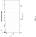
- the extent to which LEV needs to be controlled can depend on the duration of the measurements.
- the illumination typically extends for greater than 10 minutes, and in some cases, the illumination extends for hours, e.g. in some cases 10 hours or more.
- the parameters of the optical source for example a laser source, can be adjusted to attain the needed LEV suppression with the desired performance.
- the number of longitudinal modes and the spacing between the modes can be set by one of skill in the art for optimum overall performance.
- the disclosed systems and approaches can be useful in improving the effectiveness of any type of device that carries optical energy via waveguides. It can be particularly useful for devices that contain waveguides that transmit light in the visible range, for example, that transmit light from about 450 nm to about 700 nm. It can be useful for waveguides fabricated on semiconductor chips, such as silicon chips, and in particular such waveguides having a SiON core. Examples are analytical devices that measure levels of fluorescence for which the waveguides provide excitation illumination in the visible range, and planar light circuit (PLC) devices used in the visible range.
- PLC planar light circuit
- FIG. 1 shows a system or apparatus, or portion of a system or apparatus, of relevance to the instant disclosure.
- a laser or laser system 110 serving as the optical source, emits illumination light 115, also referred to as an optical excitation signal or optical excitation beam, into free space.
- the laser 110 as represented in this figure can in some cases emit light 115 directly into free space.
- the laser 110 includes other optical elements through which the light travels prior to being emitted into free space.
- the other optical elements included with the laser can include an optical fiber, a PLC, or a combination of both prior to emission of the illumination light 115 into free space.
- the illumination light emitted from the laser is sent directly to a target, for example a target device 170.
- the illumination light 115 will pass through one or more optical elements 120 which are used to shape, steer, or otherwise control the properties of the illumination light prior to reaching the target.
- the illumination light that has been shaped 117 by the one or more optical elements 120 is coupled into waveguide 140.
- the light is transmitted through waveguide 140 to an area of interest 150 on the target device.
- a coupler 130 such as a grating coupler, is used to launch the illumination light into the waveguide. While a grating coupler is shown, it is to be understood that any type of coupler, prism, or other interface optical element or method, including, for example, direct butt-coupling, can be used to direct an optical excitation signal from an optical source into the waveguide.
- Target devices that include integrated sensors will also typically include electrical outputs 175.
- the integrated sensor detects and processes an optical emission signal, and then sends electronic data related to the detected signals out of the device through the electrical output or outputs.
- the electrical outputs can, for example, be bond pads on a silicon chip, which are typically wire bonded to a chip package, and the chip package will have electronic outputs for passing on the electronic signals from the chip.
- the electronic signals are typically sent to a computer (not shown), which processes the received signals to perform the desired analysis.
- the back reflection in the waveguide can be reduced or eliminated through the use of illumination light from an optical source where the illumination light comprises multiple longitudinal modes within a narrow wavelength range.
- the illumination light comprises multiple longitudinal modes within a narrow wavelength range.
- waveguides on a target device that are single mode waveguides.
- the light introduced into these waveguides is from a laser having a single longitudinal mode (i.e., a single wavelength).
- the instant inventors have discovered that transmission of light through single mode waveguides can be improved by using an optical source having multiple longitudinal modes.
- the inventors While the presence of multiple longitudinal modes can be problematic in certain applications, in the case of fluorescence analysis systems, the inventors have found that using illumination light having multiple longitudinal modes can be done without a significant degradation in performance, because the excitation spectra of fluorescent labels typically span a relatively large wavelength range, and thus, a range of illumination wavelengths on the order of 20 nm or more can be used without a significant decrease in excitation of the fluorescent label.
- the emission spectra of fluorescent labels are typically relatively insensitive to the wavelength of the illumination light, so a spread of illumination wavelengths as described in this disclosure does not create any new issues with respect to detection of the emitted fluorescent light.
- the waveguide on the target device can be any suitable waveguide including a fiber, a planar waveguide, or a channel waveguide. Typically channel waveguides are used.
- the waveguide is preferably a single mode waveguide, but it can be a multi-mode waveguide for some applications.
- the waveguide 140 is shown as being on a target device, which can be a semiconductor chip, for example, a silicon chip.
- a target device which can be a semiconductor chip, for example, a silicon chip.
- SiON waveguides for example those formed on silicon chips.
- the SiON waveguide will have a core of SiON, and is typically surrounded by a cladding material of lower refractive index such as silicon dioxide (SiO 2 ).
- SiON can be formed in a deposition process, and the ratio of the elements can be adjusted to control the optical properties of the waveguide. For example, the ratio of oxygen to nitrogen can be varied in order to change the refractive index of the film.
- the composition is often controlled to have a refractive index greater than about 1.6, greater than about 1.7, or greater than about 1.8.
- the refractive index can be measured, for example, at the sodium D line.
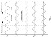
- FIG. 2 shows a flow chart outlining a proposed mechanism for the observed time-dependent back reflection or LEV.
- a standing wave pattern is formed within the waveguide (step I).
- the standing wave pattern can be formed, for example, by backscatter from a defect or reflection from a portion of the waveguide routing pattern such as an exit facet.
- step II there is a material response such as a 2-photon absorption that affects UV color centers.
- the UV absorption change can then result in a change in the refractive index at the illumination wavelength.
- the material response produces in a change in refractive index, which results in a photo-inscribed volume phase Bragg grating (step III).
- the Bragg grating can cause even more of the light to be sent back by reflection (step IV).
- the increased backward traveling light intensifies the standing wave pattern (step V).
- this step feeds back on itself, in a manner in which the initial grating can become more and more effective, sending back a higher and higher proportion of the light. This possible mechanism is consistent with the time-dependent back reflections that have been observed experimentally in such a system.
- each of the modes is now 16 times less likely to form a grating than if the power was all in a single longitudinal mode.
- the present disclosure is directed to improved systems for performing analytical operations, and particularly optical analysis of chemical, biochemical, and biological reactions for use in chemical, biological, medical, and other research and diagnostic applications.
- the systems of the disclosure are particularly well suited for application in integrated analytical components, e . g ., where multiple functional components of the overall analysis system are co-integrated within a single modular component.
- integrated analytical components e . g ., where multiple functional components of the overall analysis system are co-integrated within a single modular component.
- a number of aspects of the invention will have broad utility outside of such integrated devices and systems.
- the optical analyses that are subject of the present disclosure seek to gather and detect one or more optical emission signals from a reaction of interest, the appearance or disappearance of which, or localization of which, is indicative of a given chemical or biological reaction and/or the presence or absence of a given substance within a sample material.
- the reactants, their products, or other substance of interest (all of which are referred to as reactants herein) inherently present an optically detectable signal which can be detected.
- reactants are provided with exogenous labeling groups to facilitate their detection.
- fluorescently labeled nucleotides are used in a wide variety of different nucleic acid sequencing analyses.
- such labels are used to monitor the polymerase-mediated, template-dependent incorporation of nucleotides in a primer extension reaction.
- a labeled nucleotide can be introduced to a primer template polymerase complex, and incorporation of the labeled nucleotide into the primer can be detected. If a particular type of nucleotide is incorporated at a given position, it is indicative of the underlying and complementary nucleotide in the sequence of the template molecule.
- the detection of incorporated labeled nucleotides utilizes a termination reaction, where the labeled nucleotides carry a terminating group that blocks further extension of the primer.
- a termination reaction where the labeled nucleotides carry a terminating group that blocks further extension of the primer.
- nested sets of fragments are generated that terminate at different nucleotides.
- These fragments can then be separated by capillary electrophoresis, or other suitable technique, to distinguish those fragments that differ by a single nucleotide, and the labels for the fragments can be read in order of increasing fragment size to provide the sequence of the fragment (as indicated by the last added, labeled terminated nucleotide).
- the different nucleotides in the sequence can readily be differentiated (see, e.g., U.S. Patent No. 5,821,058
- arrays of primer-template complexes are immobilized on surfaces of substrates such that individual molecules or individual and homogeneous groups of molecules (clonal populations) are spatially discrete from other individual molecules or groups of molecules, respectively.
- Labeled nucleotides are added in a manner that results in a single nucleotide being added to each individual molecule or group of molecules. Following the addition of the nucleotide, the labeled addition is detected and identified.
- the sequencing analyses utilize the addition of a single type of nucleotide at a time, followed by a washing step.
- the labeled nucleotides that are added are then detected, their labels removed, and the process repeated with a different nucleotide type. Sequences of individual template sequences are determined by the order of appearance of the labels at given locations on the substrate.
- labeled nucleotides are observed using an optically confined structure, such as a zero mode waveguide (See, e.g., U.S. Patent No. 6,917,726 ,) that limits exposure of the excitation radiation to the volume immediately surrounding an individual primer/template polymerase complex.
- a zero mode waveguide See, e.g., U.S. Patent No. 6,917,726 ,
- the label on the nucleotide is configured to interact with a complementary group on or near the complex, e .
- a polymerase may be provided with a donor fluorophore that is excited at a first wavelength and emits at a second wavelength, while the nucleotide to be added is labeled with a fluorophore that is excited at the second wavelength, but emits at a third wavelength (See, e.g., U.S. Patent No. 7,056,661 ).
- a distinctive signal is produced.
- the various types of nucleotides are provided with distinctive fluorescent labels that permit their identification by the spectroscopic or other optical signature of their labels.
- the device may additionally include a color filter above each of the detector element, as disposed, for example, in filter layer 410.
- filter a corresponds to the color filter associated with "channel a”
- filter b corresponds to the color filter associated with "channel b”
- the set of filters is chosen to allow for a high yield of captured photons, for example with each color filter having one or more blocking bands that block the signal from a portion of one or more of the spectrally distinct signals emitted from the reaction occurring in reaction region 402.
- the filters are designed to allow passage of a large percentage of the emitted photons, while still discriminating between the four bases.
- the detector layer is operably coupled to an appropriate circuitry, typically integrated into the substrate, for providing a signal response to a processor that is optionally included integrated within the same device structure or is separate from but electronically coupled to the detector layer and associated circuitry. Examples of the types of circuitry useful in such devices are described in U.S. Patent Application Publication No. 2012/0019828 .
- the coupler on the device, it is understood that in some cases there can be a single coupler, and that in other cases, there will be a plurality of couplers on the device. Analysis devices having multiple couplers are described, for example, in U.S. Patent Application Publication No. 2016/0363728 .
- 7,194,166 discloses waveguide grating couplers suitable for coupling wavelength division multiplexed light to and from single mode and multimode optical fibers.
- the disclosed devices include a group of waveguide grating couplers disposed on a surface that are all illuminated by a spot of light from the fiber. At least one grating coupler within the group of couplers is tuned to each channel in the light beam, and the group of couplers thus demultiplexes the channels propagating in the fiber. Additional examples of grating couplers are disclosed in U.S. Patent No. 7,792,402 and PCT International Publication Nos. WO 2011/126718 and WO 2013/037900 . A combination of prism coupling and grating coupling into an integrated waveguide device is disclosed in U.S. Patent No. 7,058,261 .
- the analytical device includes a reaction cell 502 that is coupled with a reagent reservoir or fluid conduit 506, which delivers reactants to the reaction cell 502.
- the reaction cell can be a nanoscale well or zero mode waveguide. In some cases, the reaction cell will have a biomolecule such as a polymerase enzyme immobilized within it.
- the fluidic conduit can provide reagents across a number of reaction cells.
- a waveguide 514 for providing excitation illumination to the reagents within the reaction cell. The illumination light can be used to excite fluorescent emission from reagents with the reactor cell.
- Each filter layer sends the appropriate set of wavelengths of light to the appropriate pixel subset.
- the pixel subsets or sensor elements are coupled to appropriate electronic components 512, such as busses and interconnects, that make up the overall sensor or camera.
- the electronic components can also include processing elements for processing signals from the detectors.
- LEV in the SiON/SiO 2 waveguides of the subject integrated devices, LEV is more likely to be present in longer waveguides than in shorter waveguides. Without intending to be bound by theory, this observation is consistent with the proposed mechanism for LEV, as described above.
- LEV can be reduced by splitting the initially illuminated waveguide on a waveguide device into multiple waveguides.
- LEV buildup can depend on the power (or spatial power density) of the illumination light.
- the level of LEV buildup can be lowered by splitting the initial waveguide into multiple branch waveguides over a relatively short distance on the waveguide device.
- the splitting from a routing waveguide to waveguide branches in the area of interest is typically carried out near the area of interest rather than near the coupler.
- One routing waveguide per coupler is typically the most efficient approach for routing over relatively long distances. Using one routing waveguide involves fewer elements and typically uses less space on the device than when multiple routing waveguides per coupler are used.
- the current inventors have found, contrary to this typical architecture, that for waveguide devices of the instant disclosure, it can be advantageous to carry the light from the coupler to the area of interest or to a region near the area of interest over more than one waveguide per coupler, by splitting the illumination light into multiple routing waveguides near the coupler.
- the waveguide can advantageously be split into two or more waveguides, e . g . 2 to 512 waveguides, within 1 mm to 3 mm of the coupler.
- the waveguide can advantageously be split into 2 or more waveguides within 3 mm of the coupler.
- the waveguide is split into 4 or more waveguides within 3 mm of the coupler.
- the waveguide is split into 2 to 512 waveguides within 3 mm of the coupler.
- the waveguide is split into 4 to 64 waveguides within 3 mm of the coupler.
- the splitting can advantageously occur in within a fraction of the distance that the light travels from coupler to the area of interest. For example, in some cases, the splitting can occur within a distance that is less than 30% of the distance that the light travels from the coupler to the area of interest. In some cases, the splitting occurs within 20% of the distance the light travels from coupler to active area. In some cases, the splitting occurs within 10% of the distance the light travels from the coupler to the area of interest. In some cases, the coupled light is split into 2 to 512 waveguides within 20% of the distance that the light travels from the coupler to the area of interest.
- the coupled light is split into greater than 2 waveguides within 20% of the distance the light travels from the coupler to the area of interest. In some cases, the coupled light is split into greater than 4 waveguides within 20% of the distance that the light travels from the coupler to the area of interest. In some cases, the coupled light is split into 2 to 512 waveguides within 20% of the distance the light travels from the coupler to the area of interest. In some cases, the coupled light is split into 4 to 64 waveguides within 20% of the distance that the light travels from the coupler to the area of interest. Typically, for a given coupler, the most relevant distance is the longest distance traveled by the light through a branch.
- the distance over which the one waveguide is split into multiple waveguides can be the distance between the last linear portion of the waveguide before the splitter or splitters to the first linear portion of the multiple waveguides after passing through the splitter or splitters.
- the distance can also be determined by determining the distance over which the relevant power reduction has occurred (e.g. for a splitter or splitters that split the light into 4 waveguides, the distance over which a power drop of approximately one fourth has occurred, taking into account losses from the splitter or splitters).
- the splitter or splitters used to split the waveguide from the coupler into multiple routing waveguides can be any suitable type of splitter or splitters.
- the waveguide from the coupler can be split into multiple waveguides using one or more sets of binary (1:2) splitters.
- the light can be split into 4 routing waveguides using two sets of binary splitters, one binary splitter to split the light from the initial waveguide into 2 waveguides, then one binary coupler for each of these two waveguides, resulting in four routing waveguides.
- one or more higher order (1:3, 1:4, 1:5, 1:6, or even more) can be used.
- the waveguide device has a plurality of couplers, each coupling light into a single waveguide, and each of the single waveguides are split into multiple routing waveguides as described herein.
- the branch waveguides are further split near the area of interest into a large number of waveguides to monitor many reaction regions.
- the number of waveguide branches can be in the hundreds or thousands.
- the number of waveguides in the area of interest can be from about one hundred to about 10 thousand.
- each of these waveguides can illuminate from 100 to 10 thousand reaction regions, e.g. nanoscale wells or ZMWs.
- the illumination light can be split into about 1000 waveguides, each illuminating 1000 reaction regions, allowing analysis to be performed on one million reaction regions at one time.
- the number of waveguides and the number of analytical regions per waveguide can be varied in order to obtain the desired level of multiplexing and performance. For example, from 1 to 100,000 waveguides, or from 100 to 10,000 waveguides, or from 500 to 5,000 waveguides on the waveguide device can be used.
- the number of analytical regions per waveguide e.g. nanoscale wells, can be, for example, from 1 to 100,000 analytical regions, from 100 to 10,000 analytical regions, or from 500 to 5,000 analytical regions on the waveguide device can be used. Those of skill in the art will understand how to set these numbers in order to obtain the desired performance and level of multiplex.
- the light is routed such that each of the waveguides in the area of interest is illuminated from both of its ends (i.e., the waveguide is illuminated by counterpropagation from a first end and a second end of the waveguide).
- optical sources having multiple longitudinal modes can be used to provide counterpropagating illumination to the waveguides in the area of interest without significant losses due to optical interference.
- a waveguide is referred to herein as a waveguide branch.
- a waveguide branch as used herein is still a waveguide. It is referred to as a branch for clarity when discussing the splitting of light.
- a recitation of illuminating a waveguide would include illuminating a waveguide branch.
- the present invention provides optical detection systems that reduce the attenuation of optical emission signals emanating from the reaction region and ultimately, that reach the detector. This permits detection and signal discrimination that is based upon a greater amount of emitted and detected signal, thus increasing the signal-to-noise ratio.
- the optical sources for use in the systems of the instant disclosure preferably have multiple longitudinal modes spaced apart by at least 10 pm.
- the longitudinal modes are generally spaced by 10 pm to 500 pm, in some cases spaced between 10 pm and 100 pm.
- Each longitudinal mode preferably has an intensity of 20% or more of the intensity of the most intense longitudinal mode. In some cases, each longitudinal mode has an intensity of 30%, 50%, or 70% of the most intense longitudinal mode.
- the illumination spectrum, wavelength range, or bandwidth of the shortest longitudinal mode to the longest longitudinal mode is generally between 10 pm and 20 nm.
- the wavelength range is between 30 pm and 10 nm.
- the wavelength range is between 30 pm and 5 nm.
- the wavelength range is greater than 200 pm, in some cases, the wavelength range is greater than 1 nm, in some cases, the wavelength range is greater than 3 nm, in some cases, the wavelength range is greater than 5 nm, in some cases, the wavelength range is greater than 10 nm.
- the inventors have found with respect to excitation of fluorescent species that a relatively broad range of wavelengths can be used with suitable performance. For example, even wavelength ranges of the longitudinal modes of 50 nm can be used.
- the inventors have also found that if the wavelength range is too wide, there can be large losses at the coupler on the target waveguide device. While such losses will depend on coupler design, the inventors have found that in some cases a wavelength range of less than 20 nm, less than 10 nm, or less than 5 nm is preferred.
- the number of longitudinal modes can be chosen to optimize performance and cost. For example, it may be the case that using an optical source with two longitudinal modes spaced by 10 pm provides sufficient improvement in LEV, and for the other purposes described herein. In some cases, however, an optical source having eight longitudinal modes spaced apart by 30 pm may be required in order to decrease LEV to the required level. In some cases, an optical source having dozens of longitudinal modes, all within a wavelength range of 3 nm, may be the best solution. Accordingly, in some embodiments, the number of longitudinal modes is at least 2, at least 3, at least 5, at least 10, at least 15, at least 20, at least 30, at least 50, or even more.
- the amount of LEV, and other waveguide optical interference, in a given system can depend on the material and dimensions of the waveguide and on the wavelength and power of the illumination light. Those of skill in the art will understand from the teachings provided herein how to achieve a system having the desired analytical parameters.
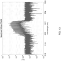
- the range of wavelengths can be determined by measuring the width of the peak, for example, determining the full width at half maximum (FWHM).
- a broadband spectrum can be synthesized by quickly scanning the laser wavelength over a particular spectral range at a particular frequency.
- the frequency of modulation can in some cases be greater than about 0.001 Hz and can in some cases be between about 1 KHz and 0.01 Hz (see para. 0008).
- the modulation of wavelength can be done at the laser, or it can be accomplished using optical elements between the laser and the target waveguide (see para. 0053).
- the frequency of modulation can depend on the time it takes for the back reflection to develop in the waveguide ( id. ) .
- the coherence function is the Fourier transform of the laser spectrum and time averaged coherence function is a Fourier transform of a time averaged optical spectrum of the laser. This will lead to at least partial suppression of the time-averaged interference effects by modulating the laser wavelength to widen the time-averaged optical spectrum.
- the laser wavelength scanning frequency is 10x larger than the chip sensor frame rate, then synchronization of the laser and the sensor in time is generally not of concern, since optical signals will be averaged over many wavelength periods during a sensor frame. In some cases it may be acceptable to work without synchronization even if laser scanning frequency is less than 10x larger than the sensor frame rate, for instance if it is only 3x larger. However, once the laser wavelength scanning frequency starts to approach the sensor frequency, it can be desirable to synchronize the laser and the sensor to ensure that each sensor frame sees exactly the same spectral range of wavelengths.
- U.S. Patent No. 7,668,216 demonstrates that a reduction of time-averaged coherence of laser radiation can be achieved by modulating a laser drive current using a modulation function optimized for obtaining a predetermined time-averaged spectral profile of laser radiation, ideally of a Gaussian shape.
- 7,668,216 shows how the fringe contrast (or coherence) is modified and fringe visibility is significantly reduced when a Gaussian shape spectrum is employed, as compared to the trapezoidal spectrum.
- OPD optical path differences
- the slow decay of the fringe contrast with increasing optical path differences (OPD) stems from the sharp edges ( ⁇ min and ⁇ max ) of the spectrum (see, e.g., FIG. 2B of U.S. Patent No. 7,668,216 ).
- OPD optical path differences
- a spectral profile that has the Fourier transform falling off most rapidly is a Gaussian profile. Therefore, in the use of such optical sources in the current applications, it is preferred to modulate the laser wavelength in such a way that the time-averaged frequency spectrum has a target spectral profile that approximates a Gaussian profile.
- the optical source utilized in the instant systems is a superluminescent light emitting diode (SLED or SLD), which is an edge-emitting semiconductor light source based on superluminescence.
- SLED superluminescent light emitting diode
- Such optical sources are also known as superluminescent diodes, superluminescence diodes, or superluminescent LEDs. They combine the high power and brightness of laser diodes with the low coherence of conventional light emitting diodes.
- the emission band of a typical superluminescent light emitting diode is approximately 5-100 nm wide. If such an optical source is designed to have a smooth Gaussian spectral distribution, its coherence function will drop on a spatial scale of few tens of microns, and there will be no repeating side lobes of the fringe visibility.
- both of the above preferred approaches rely on creating a laser spectrum of a Gaussian shape, either time-averaged or CW.
- Creation of such a laser spectrum has the advantage that just one distinct coherence peak is formed at the zero OPD point, and the coherence function falls off rapidly away from this zero OPD point. Accordingly, by the introduction of a small delay on the chip between the self-counter-propagating beams, the zero OPD point can be shifted outside of the active area everywhere on the chip for all the waveguides, and the effect of the laser coherence on detection performance can therefore be minimized.
- either CW or time-averaged CW sources can be employed for LEV suppression.
- the different sources can be utilized either for single-sided or dual-sided (i.e., counter-propagated) illumination of waveguides in the active area of the target device.
- the integrated target devices of the instant disclosure typically comprise one or more single mode waveguides.
- Single mode waveguides can be preferred for certain analyses including, for example, single molecule sequencing.
- the optical source in addition to having multiple longitudinal modes has a significant portion of its energy in a single transverse or spatial mode.
- the illumination light from the optical source has greater than 80% of its intensity in a single transverse mode, in some cases, the illumination light from the optical source has greater than 50% of its intensity in a single transverse mode, in some cases, the illumination light from the optical source has greater than 20% of its intensity in a single transverse mode, in some cases, the illumination light from the optical source has greater than 10% of its intensity in a single transverse mode.
- the illumination light from the optical source has an M 2 factor describing beam quality that is less than 1.5, in some cases, the illumination light from the optical source has an M 2 factor that is less than 1.3.
- the single transverse mode is typically the Gaussian or fundamental mode. In some cases, the single transverse mode is a TEM 00 mode.
- the illumination light from the optical source is linearly polarized.
- the characteristics of the illumination light can change along the path from exiting the optical source to the location where it illuminates a reaction region.
- the illumination light can be described as it exits the optical source, after it is emitted into free space, after it passes through optional free space optical elements, as it travels down the waveguide on the target device, and as it impinges upon the reaction region. While illumination from all of these locations will be described herein as illumination light, it is understood that the characteristics of the light at each of these points may differ. For clarity, light exiting the optical source into free space will most often be referenced. This provides a convenient point for carrying out a measurement of the properties of illumination light.
- An alternative point for determining the characteristics of the illumination light is the point after the optional free space optics and before the light enters the target device.
- the optical source will have associated optical elements such as a coupled fiber or lenses.
- free-space optical elements positioned between the optical source and the target device. These free-space optical elements can be used to modify, tune, focus, or shape the beam, for example to provide light to the target device that is coupled more effectively, or that is transmitted more effectively through the waveguide.
- the free space optical elements can be any suitable element or set of elements including, for example one or more lens, polarizer, wedge, filter, prism, mirror, or grating.
- the optical source used in the instant systems can be a laser or a laser diode
- the optical source has the properties described above with respect to minimization of LEV in the target waveguide devices.
- the optical source is a laser source. Lasers that emit in the visible wavelength range are particularly useful for the analysis systems of the present disclosure, for example lasers that emit between 450 nm and 700 nm or from 500 nm to 650 nm.
- the optical source is a superluminescent light emitting diode.
- any suitable type of laser can be used for the instant systems.
- solid state lasers are used, for example, III-V semiconductor lasers.
- Particularly useful lasers are GaInN solid state lasers.
- Lasers suitable for use in the disclosed systems, including GaInN lasers are described, for example in Sizov et al., "Gallium Indium Nitride-Based Green Lasers," J. Lightwave Technol., 30, 679-699 (Mar. 1, 2012 ), Nakamura, et al. "Current Status and Future Prospects of InGaN-Based Laser Diodes", JSAP Int. No. 1, January, 2000 , Jeong et al.
- the illumination light of the present invention While in many cases, it is most desirable to provide the illumination light of the present invention with a single optical source, for example a single laser, in some cases, it is desirable to use two or more optical sources to provide the multiple longitudinal modes that have been found to provide significant advantages for optical analysis with the instant target waveguide devices.
- the combined output of the illumination light into free space is the same as described elsewhere herein, however, in this embodiment, the output of two or more lasers is combined to produce the multiple longitudinal modes that are released into free space and then launched into the waveguides on the target device.
- the output of two or more lasers is combined to produce the multiple longitudinal modes that are released into free space and then launched into the waveguides on the target device.
- Those of skill in the art will know how to use combining optical elements to produce the desired multiple longitudinal modes of illumination light.
- the analytical devices of the disclosure are part of an analytical instrument or analytical system.
- the analytical devices can in some cases be removably coupled into an instrument or system. Reagents can be brought into contact with the analytical device before and/or after the analytical device has been coupled with the instrument or system.
- the system or instrument can provide electrical signals and/or illumination light to the analytical device, and can receive electrical signals from the detectors in the analytical device.
- the instrument or system typically has computers to manipulate, store, and analyze the data from the device.
- the instrument can have the capability of identifying the order of added nucleotide analogs for the purpose of nucleic acid sequencing. The identification can be carried out, for example, as described in U.S. Patent No. 8,182,993 , and U.S. Patent Application Publication Nos. 2010/0169026 and 2011/0183320
- the disclosure desribes analytical instruments comprising any suitable target device as described herein, an optical source for providing illumination light to the one or more waveguides of the target device or devices, an electronic system for providing voltage and current to the detector and for receiving signals from the detector; and a computer system for analyzing the signals from the detector to monitor the analytical reaction, for example to obtain sequence information about a template nucleic acid.
- a sensor or detector can comprise a single pixel. In other cases, the sensor or detector can comprise a plurality of pixels such as an array of pixels. The meaning of these terms will be understood by those of skill in the art in the context that they are used.
- PLCs Planar Lightwave Circuits
- the systems of the instant disclosure include optical delivery devices that are constructed with a plurality of integrated transmission waveguides for the delivery of optical energy from one or more optical inputs to one or more optical outputs.
- integrated devices are sometimes referred to as planar lightwave circuits (PLCs).
- PLCs are most typically found in telecommunications equipment, where they serve to couple and/or split optical excitation signals from fiber optic cores, for the purpose of, for example, multiplexing/demultiplexing, optical branching, and/or optical switching.
- FSCs fiber spacing concentrators
- PLCs typically comprise multiple components that are directly fabricated into an integrated device, where the different components provide the desired functionality.
- a PLC may comprise one or more waveguides, one or more splitters, one or more taps, one or more photodetectors, and one or more fibers, ideally polarization-maintaining fibers.
- the fibers and PLCs used in telecommunications applications typically transmit light in the infrared range, most commonly at wavelengths of about 1310 nm or about 1550 nm.
- lower cost electronics such as light-emitting diodes (LEDs) and vertical-cavity surface-emitting lasers (VCSELs) may be used in devices comprising PLCs, such as FSCs.
- LEDs light-emitting diodes
- VCSELs vertical-cavity surface-emitting lasers
- the instant optical devices are typically designed for the efficient transmission of shorter wavelengths of light.
- the optical illumination for fluorescent analysis for example in DNA sequencing reactions with fluorescently-labeled DNA reagents, is typically in the visible range, most commonly in the range from about 450 nm to about 700 nm.
- the waveguides and other components of the optical devices disclosed herein, and incorporated into the instant systems for DNA sequencing, are therefore preferably designed and scaled to transmit optical energy efficiently in the visible range.
- the wavelengths range from about 450 nm to about 700 nm.
- the wavelengths range from about 500 nm to 650 nm or even from about 500 nm to about 600 nm. In some specific embodiments, the wavelengths are from about 520 nm to about 560 nm, for example. In other specific embodiments, the wavelengths are from about 620 nm to about 660 nm, for example, approximately 635 nm or 650 nm. In some embodiments, a combination of visible wavelengths may be transmitted within the devices.
- PLC devices can include a variety of functional components embedded within the lightwave circuit.
- a device can include an optical splitter, such that a single optical input can be divided into multiple optical outputs as optical energy is transmitted through the device.
- the optical power emitted from each of the optical outputs of the device is the same, or nearly the same.
- the optical device 600 can include various integrated waveguides that are optically coupled with one another to transmit light through the device.
- the device can include an optical input 602 optically coupled through an optical input waveguide 604 to a 1x4 splitting element 608 that divides the input optical energy delivered to four optical outputs 620-623 of equal power intensity that are optically coupled to the splitting element through four optical output waveguides 610-613.
- a 1x4 splitting element 608 that divides the input optical energy delivered to four optical outputs 620-623 of equal power intensity that are optically coupled to the splitting element through four optical output waveguides 610-613.
- PLC elements suitable for use with the instant systems are described, for example in U.S. Patent Application Publication No. 2016/0273034 ,
- the disclosure provides systems comprising a target waveguide device with a single input source that can deliver light from the optical source to both ends of an optical waveguide ( i.e., by counterpropagation).
- a target waveguide device with a single input source that can deliver light from the optical source to both ends of an optical waveguide (i.e., by counterpropagation).
- counterpropagation when providing illumination to a number of regions on a target device using a single waveguide, it can be advantageous to use counterpropagating illumination. For example, as light travels through a waveguide, there are inevitable propagation losses, and therefore the regions toward the opposite end of a waveguide will receive less illumination than the regions at the beginning of the waveguide. For an optical analysis device, it is often desirable to have a consistent amount of illumination at each region, and therefore this diminishment in intensity can be undesirable. Counterpropagating illumination allows for mitigation of this issue.
- counterpropagating beams originating from the same laser and launched into a waveguide from two opposite ends can result in undesirable standing waves leading to non-uniform illumination of samples.
- the coherence length for a single-mode laser is typically very long (e.g., > 10 m) a delay line between the two beams cannot easily be introduced in order to break the coherence, especially if the splitting is done on the target device itself.
- a solution to the problem of the above-described interference is the use of two independent single-mode optical sources, each source having a different wavelength, in order to minimize or eliminate the interference.
- two optical sources When two optical sources are used, one source illuminates one end of a waveguide or set of waveguides, and the other source illuminates the other end of the waveguide or set of waveguides on the device.
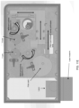
- An example of the configuration of such a target waveguide device is illustrated in FIG. 8A , where the input optical couplers are located in the lower left corner of the device.
- a 532 nm input beam is directed around the left side of the device to enter the sample waveguides from the "top" end of the device, and a 530 nm input beam is directed to enter the same sample waveguides from the "bottom” end of the device.
- a standing wave only persists on the following approximate time scale, ⁇ ⁇ 2 ⁇ f ⁇ 2 c ⁇ ⁇ 2 ⁇ ⁇ ⁇ 10 ⁇ 12 s ⁇ 1 ps , which is very short compared to the fluorescence lifetime and therefore does not have any effect on the detection system.
- the use of two single-mode optical sources with different wavelengths can mitigate or solve the problem of interference due to counterpropagating illumination, the use of two optical sources is expensive and adds to the complexity of the illumination system.
- FIG. 8B An example of the configuration of such a target device is illustrated in FIG. 8B , where the input optical couplers are located in the lower left corner of the device.
- a single 522 nm multi-longitudinal mode laser provides the optical input at both of the indicated input couplers.
- the two beams are directed around the device so that they enter the same sample waveguides from opposite ends, thus providing counterpropagating input light.
- a single coupler on the target device could receive input optical energy from a single optical source, and the separate optical inputs for the two ends of the sample waveguides could be created by splitting the light on the target device itself.
- one aspect of the disclosure involves the illumination of a target waveguide device, wherein the waveguide is illuminated by splitting the light from a single optical source such that the waveguide is illuminated from both of its ends.
- the single optical source emits illumination light into free space prior to coupling into the target device.
- the emitted illumination light comprises multiple longitudinal modes spaced apart by at least 10 pm.
- each longitudinal mode having an intensity of 20% or more of the intensity of the most intense longitudinal mode, wherein the wavelength range of the shortest longitudinal mode to the longest longitudinal mode is between 10 pm and 20 nm.
- the characteristics of the broadband optical source for use in counterpropagation are provided throughout this application.
- the target device has multiple waveguides, and the single optical source is used to illuminate each of the waveguides from each of its ends.
- a single coupler on the target device is used to collect the light from the single illumination source.
- the light from this source is routed on the device to the two ends of a single waveguide or a set of waveguides.
- the target waveguide device comprises a plurality of optical waveguides, each optical waveguide comprising a first end and a second end, and wherein the first end of each optical waveguide and the second end of each optical waveguide are configured to receive the optical excitation beam from the optical source. More specifically, the target the target waveguide device can comprise at least 2, at least 5, at least 10, at least 50, at least 100, at least 500, at least 1,000, at least 5,000, at least 10,000, at least 50,000, or even more optical waveguides.
- the target waveguide device can comprise no more than 100,000, no more than 50,000, no more than 10,000, no more than 5,000, no more than 1,000, no more than 500, no more than 100, or even fewer optical waveguides.
- the set of waveguides can be, for example, from 1 to 100,000 waveguides, from 100 to 10,000 waveguides, or from 500 to 5,000 waveguides.
- the ability to use a single coupler to provide this counterpropagating light can be advantageous, as it can significantly lower costs and reduce the complexity of the illumination system, in particular when compared to systems where multiple light beams must simultaneously be directed to multiple different couplers on the target device.
- the routing of light on the device can be achieved by including one or more embedded optical splitters in the device between the input coupler and the waveguide, or set of waveguides, that provide illumination to the reaction region, as would be understood by those of ordinary skill in the art.
- the disclosure provides systems and methods for using signals from the target optical device itself in order to perform source-to-device alignment, in some cases with a single input coupler.
- alignment of an illumination light beam from a laser or other optical source (where the source is typically part of an analytical instrument, such as a sequencing instrument) with an optical target device (which is often removably held in place in the instrument) such that the light beam is precisely directed to the coupler on the target device can be a difficult problem.
- the components in the instrument responsible for holding a removable target device in place may have geometrical uncertainties, while on the other hand, there may also be uncertainties in the position of the coupler on the target device, for example, with respect to the edge of the chip, given that imperfections of the cell packaging process can be +/- 300 ⁇ m or larger in the x and y directions.
- the beam from the optical source also may need to be directed to the coupler on the target device at a certain angle in order to maximize the coupling efficiency, and the optimal angle can also vary from target device to target device.
- FIG. 9 illustrates an optical analytical system that comprises an alignment camera.
- the requirement for an analytical system to include an alignment camera increases the complexity of the system as well as the cost.
- the instant disclosure thus also describes systems, devices, and processes for carrying out and optimizing alignment between an optical source, in particular a laser source, and a target device, in particular a waveguide device comprising at least one input optical coupler, for example a DNA sequencing chip.
- the alignment process can include both a coarse alignment and a fine alignment.
- the alignment can be done by using signal feedback directly from a sensor that is incorporated into the target device, for example an analytical sequencing chip, and adjusting the position of the optical source relative to the target device in order to maximize this signal.
- a raster scan can be performed with the laser beam over the area where an input coupler is expected to be located, and a signal from one or more sensors optically coupled to the an optical waveguide associated with the coupler can be monitored. Since alignment is routinely done over a short period of time (compared to the duration of, for example, a sequencing analysis on a sequencing chip) and at low power, the relative photodamage to a sample in the reaction region is small as the alignment is achieved.
- the fluorescent signal arising from one or more reaction regions is generated in response to the input light.
- the same optical and data paths can be used both for the alignment process and for subsequent analytical measurements, where an "optical alignment signal” is obtained during the alignment process, and an “optical emission signal” is obtained during the analytical measurments.
- signals can be binned together from several sensor regions ( e . g ., from several pixels on the detector), for example using embedded software, to improve the signal-to-noise ratio of the feedback signal.
- the regular data analysis pipeline can be slow, since all of the sensor regions from the sensor need to be processed. Therefore, in alternative embodiments, signals from several reaction reactions in the sensor board can be binned (for example by reprogramming the device using a field-programmable gate array (FPGA)), and the resultant signal can be fed to the computer controlling the alignment motion between the optical source and the target device via a separate data path.
- FPGA field-programmable gate array
- a fluorophore or another agent capable of generating an optical emission signal with intensity that varies as a function of input optical energy
- a fluorophore or another agent capable of generating an optical emission signal with intensity that varies as a function of input optical energy
- the subsequent fine alignment step which optimizes the position between the optical source and the target device, should be easier to perform compared to the coarse alignment, since after the coarse alignment step is complete, signals emitted from the actual reaction regions can be monitored and maximized, for example using an optimization method such as a Nelder-Mead method, or the like, as would be understood by those of ordinary skill in the art.
- a target device can have a small auxiliary alignment sensor, either 2D, 1D, or two orthogonally positioned 1D, placed near the input coupler at a distance precisely defined using lithography step during chip manufacturing.
- the dimensions of the auxiliary alignment sensor should be larger than its positioning uncertainty during packaging, to ensure that the laser beam will be registered on the sensor as soon as the cell is placed in the instrument.
- the geometrical tolerances of the components responsible for target device within the instrument can also be of importance in these considerations. For example, if the packaging uncertainty of the auxiliary alignment sensor on the target device is +/-300 microns, then the size of the sensor should preferably be larger than 600 microns.
- auxiliary alignment sensor Since the auxiliary alignment sensor is placed on the target device very precisely with respect to the input coupler, once the input optical beam is registered on the auxiliary alignment sensor, it is immediately known by how much the beam and/or target device needs to be shifted in order to align the input beam with the input coupler. Achieving sub-micron positioning accuracy using lithographic processes is well within the skill in the art. If there is expected to be some degree of rotation and cross-coupling between the x and y axes of the target device, then the beam can first be scanned over the sensor to determine the required rotation angle.
- the sensor can either be a part of the sensor responsible for detecting signals from the reaction regions or can preferably be a separate sensor, as it can optionally include an intervening filter layer in order to attenuate the laser beam to a level that does not cause saturation of the sensor output.
- the locations of different alignment features e.g., auxiliary alignment sensors, auxiliary alignment couplers, and the like
- E 2 PROM Electrically Erasable Programmable Read-Only Memory
- positions of the input couplers with respect to known datum or distance between the alignment feature, or features, and the input coupler can be precisely measured. If the offsets related to the cell positioning in the instrument are also precisely calibrated, then utilizing this information can allow for significant speed up of the alignment time.
- a quad-cell consisting of 4 larger size detectors packed together, for example in a square configuration, can be employed.
- two detectors can be used to determine the position of the beam along one axis, and two detectors can be used along the other axis.
- the beam is initially centered in the middle of the quad-cell, and it is then translated to the input coupler using the known separation distance, as described above.
- one or more auxiliary alignment couplers can be placed at a lithographically defined distance from the input coupler that is optically connected to the sequencing area, and the one or more auxiliary couplers can be used to assist in coarse alignment.
- the one or more auxiliary couplers can be used to assist in coarse alignment.
- from one to six, from one to four, from one to three, or from one to two auxiliary couplers can be arranged on the target device to provide coarse alignment.
- four auxiliary input couplers can be packed close to each other in a rectangular shape configuration, for example in a square shape configuration, where one of the four couplers is the actual input coupler.
- One advantage of having several input couplers is the increased probability that the laser will encounter one of them during the alignment scan.
- the auxiliary couplers are preferably placed far enough apart on the surface of the optical device that an input beam scanning the surface of the device will be ensured of encountering at least one of them during the coarse alignment process, given manufacturing tolerances of the optical device.
- the light entering the device from the auxiliary couplers can be routed to the active area sensor or to a sensor that is dedicated to the alignment process.
- the system for carrying out coarse alignment can include an expanding lens, including a cylindrical lens, within the laser beam path to broaden the laser beam spot on the coupler.
- the beam can be broadened by the insertion of a diffractive optical element (DOE) in the beam path, thus also reducing the coarse alignment time.
- DOE diffractive optical element
- the fine alignment step is performed, for example by maximizing the sequencing signal strength through the sample input coupler.
- the expanded beam can enable coarse alignment through a sample input coupler, without the need for an auxiliary input coupler on the target device.
- the expanded beam can be coupled through one or more auxiliary couplers to achieve coarse alignment.
- Fine alignment is typically achieved using the sample input couplers, for example, after removing the expanding lens from the path of the optical source.
- the amount of beam expansion ideally should be larger than the uncertainty of the coupler position to ensure that the input or auxiliary input coupler will be encountered by the expanded beam in that dimension.
- the laser power density can be too low after beam expansion, and it may become more difficult to detect the alignment signal.
- the additional lens will typically be removed from the optical path to proceed with a fine alignment.
- the lens is not exactly orthogonal to the optical beam, removing the lens from the beam path may result in the beam becoming misaligned with the input coupler.
- Such displacement caused by the lens can be calibrated during instrument manufacturing and beam position can be corrected after the additional lens is removed.
- auxiliary sensor such as a quad-cell or sensor or a photodiode
- some auxiliary features for example, diffractive features on the target device at a known, lithographically defined distance from the input coupler to assist with the coarse alignment process.
- a sensor either 2D or 1D, or a photodiode
- the sensor position can be arranged in such a way that if the laser is scanned over the target device surface and hits a diffractive feature the light will be deflected towards the sensor. This approach can help to quickly localize the position of the input coupler, thereby speeding up the coarse alignment search.
- the alignment process can be performed by holding the target device in a fixed position and scanning the output from the optical source across the surface of the immobilized device, it should be understood that the process can alternatively be performed by holding the optical source in a fixed position and moving the target device relative to the output from the optical source in order to achieve alignment.
- either the target waveguide device or the optical source is movable relative to the other in at least two dimensions, and alignment is achieved by configuring the system to monitor an optical alignment signal and to move either the target waveguide device or the optical source relative to the other to increase the optical alignment signal.
- the system does not include an alignment camera.
- the system is configured to move the target waveguide device relative to the optical source until the optical alignment signal is increased to a maximum level.
- At least one detector region in the target waveguide device is configured to detect both an optical alignment signal and an optical emission signal.
- the target waveguide device further comprises an auxiliary alignment sensor, and the auxiliary alignment sensor is positioned on a surface of the target waveguide device at a distance from the at least one optical coupler that is precisely defined using photolithography during manufacture of the target waveguide device.
- the waveguides of the target waveguide device are configured to transmit counterpropagated optical signals, as described in detail above, for example, by a single optical source, such as a broadband, multimodal optical source.
- the target waveguide devices used in the just-described systems and methods for alignment can alternatively or in addition include any of the above-described target waveguide device features, without limitation.
- the optical beam is configured or scanned spatially to project at least a coarse illumination spot size and a fine illumination spot size, wherein the coarse illumination spot size is larger than the fine illumination spot size. More specifically, in these embodiments, the optical beam can be configured to project the coarse illumination spot size on the target waveguide device while the target waveguide device or the optical beam are moved relative to one another to increase the optical alignment signal.
- the disclosure provides improved optical systems for the delivery of optical energy to a target device in a controllable manner.
- optical systems include at least two translating lenses, positioned between the optical source and the target device, to control the delivery of light from a laser or other optical source through an optical beam in multiple directions.
- FIGs. 10A-10D An exemplary schematic design of a single-beam optical system with two translatable lenses (also referred to as a "light pen") is illustrated in FIGs. 10A-10D .
- This design is significantly simpler and less expensive than that of a system comprising an optical source designed to simultaneously illuminate multiple input couplers on a chip. See, e.g., the "light brush” and other optical delivery devices described in U.S. Patent Application Publication Nos. 2016/0273034A1 and 2016/0363728A1 .
- delivery of light from an optical source is controlled by at least two translating lenses positioned between the optical source (located at the top of each drawing) and a removable target waveguide device (located at the bottom of each drawing), where the optical beam is illustrated passing through the lenses in each drawing.
- an optical source for example a fiber
- a translatable collimator lens (1001)
- the collimator lens and the optical source e.g., an optical fiber
- the collimated light is then focused by a translatable objective lens (1002) onto the input coupler of a target device (1003).
- target waveguide devices also referred to as "chips”
- yaw angle i.e., a first direction, a second direction, a first angle, and a second angle
- FIG. 10A Note that the yaw angle lays in the orthogonal plane relative to the page and is therefore not shown in the drawing.
- Error in yaw can often be very small, however, in which case control along the yaw axis may not be needed.
- the incoming (pitch or yaw) angle changes, while the spatial (x,y) position on the target device does not change.
- the dashed line in FIGs. 10A and 10B is intended to indicate that the objective lens remains fixed in these examples.
- the beam can be translated in the x or y spatial direction, as desired.
- the beam can be translated in the x or y direction by moving only the objective lens.
- the focal length of the objective lens is 100 mm, and the required x or y motion is at most about +/-300 ⁇ m, then the cross-coupling between the angle and the horizontal motion will lead to less than a +/-0.2 deg angle change in the incidence angle.
- the just-described systems for optical analysis in which at least two translating lenses are used to control the delivery of an optical signal from an optical source to a target device, are generally applicable to the coupling of optical signals from a variety of optical sources to a variety of target devices.
- these approaches are usefully applied in systems with target devices that have at least one optical coupler configured to receive the optical excitation beam through free space from the optical source.
- the target waveguide device advantageously comprises a plurality of optical waveguides, the optical waveguides configured to receive the optical excitation beam from the at least one optical coupler.
- the target waveguide device can comprise at least 2, at least 5, at least 10, at least 50, at least 100, at least 500, at least 1,000, at least 5,000, at least 10,000, or at least 50,000 optical waveguides.
- the target waveguide device can comprise no more than 100,000, no more than 50,000, no more than 10,000, no more than 5,000, no more than 1,000, no more than 500, or no more than 100 optical waveguides.
- the target waveguide device can comprise from 1 to 100,000, from 100 to 10,000, or from 500 to 5,000 optical waveguides.
- the target waveguide device of the disclosed systems comprises at least one optical splitter, wherein the at least one optical splitter comprises an optical input and a plurality of optical outputs, and wherein the optical input of the at least one optical splitter is configured to receive the optical excitation beam from the optical coupler.
- Such devices also typically comprise a plurality of optical waveguides, the optical waveguides configured to receive the optical excitation beam from the plurality of optical outputs of the at least one optical splitter.
- the target waveguide device of the instant systems comprises no more than one optical coupler for providing illumination light to reaction regions.
- the at least one optical splitter comprises 2 to 512 optical outputs.
- the systems comprising at least two translating lenses, positioned between the optical source and the target device, to control the delivery of light from a laser or other optical source in multiple directions can also advantageously be combined with any of the other above-described systems and methods, including the more specific embodiments of those systems and methods.
- the optical source of the instant systems emits a broadband, multimodal optical excitation beam, for example an optical excitation beam comprising at least 3, at least 5, at least 10, at least 15, at least 20, at least 30, or at least 50 longitudinal modes.
- the target waveguide device of the instant systems is any of the above-described target waveguide devices, including those configured to receive excitation light provided by counterpropagating optical beams.
- FIG. 11A shows two views of a suitable cam with the rotational axis offset from the centroid of the cam.
- FIG. 11B shows the displacement of such an offset cam (in mm) as a function of the cam angle (in degrees) as the cam rotates around the axis.
- Such eccentric cams can be driven by any suitable motor means, as would be understood by those of ordinary skill in the art. They are preferably driven using an inexpensive stepper motor, such as a stepper motor with an integrated planetary gearbox.
- an eccentric cam control can provide the following exemplary specifications: Property (AT/CT) Value Travel +/- 1 mm Resolution 0.1 ⁇ m Property (Pitch) Value Travel +/- 5 mm Resolution 0.5 ⁇ m It should be understood, however, that a wide variety of other specified values can be achieved by varying the properties of the stepper motor and the dimensions and eccentricity of the cam, as would be understood by those of ordinary skill in the art.
- FIG. 11C illustrates how an eccentric cam controlling mechanism can be mechanically coupled to a lens, for example a collimator lens, to provide the desired fine motion control of the lens in a single dimension.
- FIG. 11C also illustrates other optional features and components of such a control mechanism, for example a "linear guide” mechanism, to maintain and control motion of the lens in a single direction, and a "spring force” mechanism, to provide a tensioning force between the lens-holding stage and the eccentric cam, as the cam is rotated by the stepper motor.
- a roller mechanism attached to the lens stage can also be used to provide a smooth connection between the eccentric cam and the lens stage, as shown in this drawing.
- stepper motor and “gear box” are chosen to provide the desired functionality, as would be understood by those of ordinary skill in the art.
- a stepper motor with an integrated planetary gearbox can be chosen to provide a 100:1 gear reduction, a 0.018° step size, a 4 Nm maximum torque, and can be non-backdriveable, but any suitable stepper motor and gear box can be chosen and adapted for use in the above drive systems provided the specifications are appropriate for the desired use.
- FIG. 11D illustrates the control of an objective lens in two spatial dimensions (AT and CT) using two stationary stepper motors and their associated eccentric cams to drive a lens mount along two orthogonal axes.
- FIGs. 11E and 11F provide two different views of an assembled optical alignment system that controls an objective lens in two orthogonal directions (X and Y) and that also controls the pitch angle of a collimation lens. Accordingly, in this system, fine motion control is provided for a lens-holding optical stage along three separate axes (e.g., AT, CT, and pitch).
- motion along additional axes can be readily achieved in such a system through the addition of suitable motor/cam/linear- or rotational-guide mechanisms for each additional axis of motion.
- motion is controlled along four separate axes (e.g., AT, CT, pitch, and yaw).
- motion is controlled along five separate axes (e.g., AT, CT, pitch, yaw, and roll) or even six separate axes, in order to provide the desired relative positioning and alignment between the optical source and the target waveguide device.
- the above designs provide significant advantages over traditional designs for controlling lens translation in two dimensions.
- the motor controlling lens movement along the first directional axis e.g., the AT axis
- the motor and guide mechanism controlling lens movement along the second directional axis e.g., the CT axis
- the weight of the motor and associated mechanical components can therefore significantly increase the costs of the AT components, which must overcome the inertia of the entire CT drivetrain.
- the chips of any of the above systems and methods can in some embodiments comprise at least one coupler.
- chip and “target waveguide device” are generally used interchangeably herein, unless the context makes clear otherwise.
- FIG. 9 shows a typical setup that can be used for sending light into a target waveguide device and measuring the amount of light transmitted as well as the amount of reflected over time.
- the light can either be delivered to one side of the target device using one of the lasers or to both sides of the device using both lasers.
- the alignment camera measures light sent through the waveguides and then coupled out of the device.
- the target device includes a zero mode waveguide (ZMW) region for carrying out fluorescent analyses, such as single molecule real time sequencing as described herein.
- ZMW zero mode waveguide
- FIG. 12 shows a set of measurements that illustrate the time-dependent back reflection.
- Light is sent into the waveguide at about 532 nm.
- the top curve, axis to the left, shows reflected light over time.
- the lower curve, axis to the right, shows transmitted light. It can be seen that over time there is a buildup in back reflection that occurs at the expense of transmitted light.
- FIG. 13 shows the wavelength spectrum of the output from a 522 nm broadband direct band gap diode laser.
- the laser has a single transverse spatial mode structure with beam quality M 2 ⁇ 1.2 (nearly diffraction limited).
- the laser displays multiple longitudinal modes, which make it broadband with spectral linewidth (wavelength range) of ⁇ 1-2 nm.
- the maximum fiber coupled power output is about 55 mW, and the temporal stability is +/- 0.5%.
- FIG. 14 shows that no LEV was observed during a 24-hour exposure when the broadband laser with the maximum incident laser power of 54 mW was coupled to a target device with SiON waveguides.
- FIG. 15 shows a control experiment on the same target device, when the device was illuminated with 532 nm single longitudinal mode laser at comparable laser power. As is clear from this experiment, there is a significant drop in transmitted power over two hours when using the single longitudinal mode laser. This drop in transmitted power is characteristic of LEV.
- the instant inventors have discovered that the poor performance typically observed using counterpropagated, single-wavelength, narrowband optical excitation in a target waveguide device can be overcome through the use of a broadband multi-mode laser input source.
- the utility of this approach has been demonstrated in exemplary DNA sequencing experiments using a PacBio ® Sequel ® chip that has been illuminated by light from a single broadband, multi-mode laser source.
- excitation power was provided from the single laser source by splitting the laser output and coupling the separate beams into a DNA sequencing device, for example a device having the optical pathways illustrated in the device of FIG. 8B .
- the optical input was provided by a direct band-gap multi-mode InGaN semiconductor diode laser, which delivered a fiber-coupled power of up to 55 mW (77 mW laser head power), a central wavelength of about 522 nm, and a spectral bandwidth of approximately 2 nm.
- This laser source is well coupled into the target device and, as shown in FIG. 14 , eliminates the generation of LEV in the target optical waveguides.
- FIG. 16 A signal-to-noise ratio heat map generated from such an exemplary DNA sequencing reaction using the above-described laser source and target device is illustrated in FIG. 16 , where the laser power at the head was 37 mW, and the power per cell input coupler was 2.4 mW.
- a 30 kB E.coli fragment was sequenced for 10 hours in this experiment.
- the SNR heat map shown in FIG. 16 was obtained from a 5 minute movie that was captured early in the sequencing run. Results of this sequencing run showed an 88.7% accuracy, a 10.1 kB read-length, and a 2.0 GB sequencing yield on just one half of a standard Sequel ® chip.
- FIG. 17 illustrates the effect of laser power on wavelength bandwidth.
- the spectrum of a 522 nm multimode laser starts to narrow significantly as the power of the laser is decreased below about 20 mW.
- FIG. 18 illustrates the effect of laser coherence on sequencing SNR heatmaps, and the corresponding sequencing accuracy, as laser power is decreased. As can be seen in this example (including the analysis described below for FIG. 20 ), a significant decrease in sequencing accuracy is observed where the laser head power is decreased below about 20 mW.
- FIG. 19 describes the relationship between laser coherence, optical modes, spectral width, and optical path difference (OPD).
- the index of refraction n chip can be estimated using a typical laser spectrum, as shown in the lower left portion of FIG. 19 .
- the illustrated spectrum has about 36 optical longitudinal modes spanning ⁇ 2 nm, giving a mode spacing of ⁇ 1 ⁇ 55 pm or ⁇ v 1 ⁇ 0.61 ⁇ 10 11 Hz.
- the coherence length on the target device can be estimated to be about 31.6 ⁇ m. Since the coherence fringes are repeating in the active area of the cell, with the period of ⁇ 1.3 mm, less than about 3% of ZMWs are experiencing higher coherence and even for smaller percentage of ZMWs it results in significant yield loss.
- Experimentally comparing yields for illumination scheme using the self-counter-propagation from one laser vs. counter-propagation from two lasers no yield difference was observed given the experimental uncertainty.
- the degree of laser coherence is a strong function of the number of modes and for two beams of the same amplitude and polarization can be theoretically described by the following dependence ⁇ sin N ⁇ x N sin ⁇ x , where x is the OPD between the self-counter-propagating beams with respect to the zero OPD point normalized by the period of the coherence function.
- x is the OPD between the self-counter-propagating beams with respect to the zero OPD point normalized by the period of the coherence function.
- FIG. 19 illustrates the appearance of a slowly decaying coherence function.
- This figure is adapted from Epworth (1982) "The Temporal Coherence of Various Semiconductor Light Sources Used in Optical Fibre Sensors” in “Fiber-Optic Rotation Sensors and Related Technologies", Eds. S. Ezekiel and H.J. Arditty, pp. 237-244 .)
- FIG. 17 , 18 , and 20 provide additional support to the notion that high degree of coherence is undesirable for active area illumination.
- SNR heatmaps exhibit significantly larger spatial variations (see FIG. 18 ).
- FIG. 20 also shows that the accuracy of sequencing data decreases as the laser spectrum gets narrower. The six data points in FIG.
- a 7.7 mW laser input ( ⁇ 0.5 mW per coupler), (2) a 10 mW laser input ( ⁇ 0.65 mW per coupler), (3) a 15 mW laser input ( ⁇ 1.0 mW per coupler), (4) a 25 mW laser input ( ⁇ 1.6 mW per coupler), (5) a 37 mW laser input ( ⁇ 2.4 mW per coupler), or (6) a 61.6 mW laser input ( ⁇ 4 mW per coupler).
- FIGs. 21A-21C illustrate requirements for achieving coarse alignment between a laser beam and a target waveguide device, specifically a DNA sequencing chip, in an optical system with no alignment camera.
- optical signals emitted by fluorescent reagents in the reaction regions of an arrayed waveguide device are measured as an indication of the efficiency of coupling of an input optical source and thus the alignment of the device with the source.
- the fluorescent signals are collected on a +/- 40 micron grid with 10 microns resolution in x and y and range of +/- 0.5° with 0.25° resolution in pitch angle with respect to the optimal alignment point.
- the same set of data is plotted as a function of 3 different coordinates in FIGs. 21A-21C .
- the laser beam is preferably within about +/- 20 microns in x (21A) and y (21B) coordinates (called AT and CT on the plots) and within about +/- 0.5° in pitch of the optimum alignment point in order to excite fluorescent signal, which can be subsequently detected by the chip sensor.
- the fluorescent signal is an average over 3x3 camera pixels in the sequencing area, and this averaging can be done quickly in the FPGA.
Landscapes
- Physics & Mathematics (AREA)
- General Physics & Mathematics (AREA)
- Health & Medical Sciences (AREA)
- Optics & Photonics (AREA)
- Chemical & Material Sciences (AREA)
- Immunology (AREA)
- Life Sciences & Earth Sciences (AREA)
- Analytical Chemistry (AREA)
- Biochemistry (AREA)
- General Health & Medical Sciences (AREA)
- Pathology (AREA)
- Engineering & Computer Science (AREA)
- Microelectronics & Electronic Packaging (AREA)
- Nuclear Medicine, Radiotherapy & Molecular Imaging (AREA)
- Chemical Kinetics & Catalysis (AREA)
- Plasma & Fusion (AREA)
- Investigating, Analyzing Materials By Fluorescence Or Luminescence (AREA)
- Investigating Or Analysing Materials By Optical Means (AREA)
Claims (20)
- Système d'analyse optique, le système comprenant :
une source optique (110), dans lequel la source optique est un laser ou une diode laser, et un dispositif de guide d'ondes cible amovible, comprenant :au moins un coupleur optique (130), le au moins un coupleur optique étant configuré pour recevoir un faisceau d'excitation optique (115) à travers un espace libre à partir de la source optique ;au moins un guide d'ondes optique (140), le au moins un guide d'ondes optique comprenant une première extrémité ; dans lequel la première extrémité du guide d'ondes optique est configurée pour recevoir un signal d'excitation optique à partir du au moins un coupleur optique ;au moins une région de réaction (155, 302, 402, 502), la au moins une région de réaction étant optiquement couplée au au moins un guide d'ondes ; etau moins une région de détection (180, 320, 510), la au moins une région de détection étant configurée pour détecter un signal d'émission optique à partir de la au moins une région de réaction ; caractérisé en ce que le faisceau d'excitation optique est un faisceau d'excitation optique multilongitudinal à large bande. - Système selon la revendication 1, dans lequel le dispositif de guide d'ondes cible comprend en outre :au moins un séparateur optique (608) ;dans lequel le au moins un séparateur optique comprend une entrée optique (602) et une pluralité de sorties optiques (620-623), dans lequel l'entrée optique du au moins un séparateur optique est couplée optiquement au au moins un coupleur optique ; etdans lequel la première extrémité du guide d'ondes optique est configurée pour recevoir le signal d'excitation optique à partir du au moins un coupleur optique, à travers l'entrée optique du au moins un séparateur optique (608), et à travers une première sortie optique (620-623) du au moins un séparateur optique.
- Système selon la revendication 1, dans lequel le au moins un guide d'ondes optique comprend une seconde extrémité ; dans lequel la seconde extrémité du au moins un guide d'ondes optique est configurée pour recevoir le signal d'excitation optique depuis la source optique.
- Système selon la revendication 3, dans lequel le dispositif de guide d'ondes cible comprend en outre :au moins un séparateur optique (608) ;dans lequel le au moins un séparateur optique comprend une entrée optique (602) et une pluralité de sorties optiques (620-623), dans lequel l'entrée optique du au moins un séparateur optique est couplée optiquement au au moins un coupleur optique ; etdans lequel la première extrémité du au moins un guide d'ondes optique est configurée pour recevoir le signal d'excitation optique depuis une première sortie optique (620-623) du au moins un séparateur optique (608), et la seconde extrémité du au moins un guide d'ondes optique est configurée pour recevoir le signal d'excitation optique depuis une seconde sortie optique du au moins un séparateur optique.
- Système selon l'une quelconque des revendications 2 à 4, dans lequel le au moins un séparateur optique (608) comprend de 2 à 512 sorties optiques (620-623).
- Système selon la revendication 3 ou la revendication 4, dans lequel le dispositif de guide d'ondes cible comprend : un premier coupleur optique et un second coupleur optique, dans lequel la première extrémité du guide d'ondes optique est configurée pour recevoir le signal d'excitation optique depuis le premier coupleur optique, et la seconde extrémité du guide d'ondes optique est configurée pour recevoir le signal d'excitation optique depuis le second coupleur optique.
- Système selon l'une quelconque des revendications 1 à 6, dans lequel le système comprend une source optique unique (110).
- Système selon l'une quelconque des revendications 1 à 6, dans lequel le faisceau d'excitation optique (115) comprend une pluralité de modes longitudinaux, facultativement dans lequel le faisceau d'excitation optique comprend au moins 3, au moins 5, au moins 10, au moins 15, au moins 20, au moins 30 ou au moins 50 modes longitudinaux.
- Système selon l'une quelconque des revendications 1 à 6, dans lequel :(a) le faisceau d'excitation optique (115) comprend un spectre à large bande d'onde continu ; ou(b) le faisceau d'excitation optique (115) comprend un spectre à large bande moyenné dans le temps ; ou(c) le faisceau d'excitation optique (115) comprend un mode transversal unique, facultativement dans lequel le mode transversal unique est un mode gaussien.
- Système selon l'une quelconque des revendications 1 à 6, dans lequel le faisceau d'excitation optique (115) affiche un point de différence de trajet optique zéro, et le dispositif de guide d'ondes cible est configuré pour décaler le point de différence de trajet optique zéro à l'extérieur du au moins un guide d'ondes optique.
- Système selon l'une quelconque des revendications 1 à 6, dans lequel le dispositif de guide d'ondes cible comprend une pluralité de guides d'ondes optiques, chaque guide d'ondes optique étant configuré pour recevoir le signal d'excitation optique depuis la source optique, facultativement dans lequel le dispositif de guide d'ondes cible comprend (i) au moins 2, au moins 5, au moins 10, au moins 50, au moins 100, au moins 500, au moins 1 000, au moins 5 000, au moins 10 000, ou au moins 50 000 guides d'ondes optiques ; ou (ii) dans lequel le dispositif de guide d'ondes cible comprend pas plus de 100 000, pas plus de 50 000, pas plus de 10 000, pas plus de 5 000, pas plus de 1 000, pas plus de 500, ou pas plus de 100 guides d'onde optiques ; ou (iii) dans lequel le dispositif de guide d'ondes cible comprend de 1 à 100 000, de 100 à 10 000, ou de 500 à 5 000 guides d'ondes optiques.
- Système selon l'une quelconque des revendications 1 à 6, comprenant en outre au moins un élément optique positionné entre la source optique et le dispositif de guide d'ondes cible, dans lequel le au moins un élément optique module le faisceau d'excitation optique entre la source optique et le dispositif de guide d'ondes cible, facultativement dans lequel le au moins un élément optique est une lentille, un polariseur, un coin, un filtre, un prisme, un miroir ou un réseau.
- Système selon l'une quelconque des revendications 1 à 6, comprenant en outre un ordinateur qui reçoit au moins un signal électronique depuis la au moins une région de détection et analyse le au moins un signal électronique, facultativement dans lequel l'analyse comprend l'obtention d'informations de séquençage d'acide nucléique.
- Système selon l'une quelconque des revendications 1 à 6, dans lequel le faisceau d'excitation optique multilongitudinal à large bande présente une longueur d'onde d'environ 450 nm à environ 700 nm, facultativement dans lequel la longueur d'onde est d'environ 500 nm à environ 650 nm.
- Système selon l'une quelconque des revendications 1 à 6, dans lequel le au moins un guide d'ondes optique (102) comprend un noyau de SiON, facultativement dans lequel le noyau de SiON présente un indice de réfraction supérieur à environ 1,6.
- Système selon l'une quelconque des revendications 1 à 6, dans lequel le au moins un guide d'ondes optique (102) comprend un noyau entouré de dioxyde de silicium, ou dans lequel le dispositif cible est fabriqué sur une puce de silicium.
- Système selon l'une quelconque des revendications 1 à 6, dans lequel la au moins une région de détection (180, 320, 510) comprend un capteur CMOS.
- Système selon l'une quelconque des revendications 1 à 6, dans lequel :(a) la source optique (102) est couplée à une fibre optique, et le faisceau d'excitation optique (115) est émis à partir de la fibre optique ; ou(b) la source optique (102) est couplée à un circuit d'ondes lumineuses planaire à travers une fibre optique, et le faisceau d'excitation optique est émis à partir du circuit d'ondes lumineuses planaire.
- Système selon l'une quelconque des revendications 1 à 6, dans lequel la au moins une région de réaction comprend un puits à l'échelle nanométrique.
- Système selon l'une quelconque des revendications 1 à 6, dans lequel :(a) le dispositif de guide d'ondes cible comprend de 2 à 16 coupleurs optiques ; et/ou(b) le dispositif de guide d'ondes cible comprend de 2 à 16 séparateurs optiques.
Priority Applications (1)
| Application Number | Priority Date | Filing Date | Title |
|---|---|---|---|
| EP25170214.8A EP4560368A3 (fr) | 2017-11-03 | 2018-11-03 | Systèmes, dispositifs et procédés pour une transmission et un alignement de guide d'ondes optique améliorés |
Applications Claiming Priority (2)
| Application Number | Priority Date | Filing Date | Title |
|---|---|---|---|
| US201762581203P | 2017-11-03 | 2017-11-03 | |
| PCT/US2018/059112 WO2019090192A1 (fr) | 2017-11-03 | 2018-11-03 | Systèmes, dispositifs et procédés pour une transmission et un alignement de guide d'ondes optique améliorés |
Related Child Applications (1)
| Application Number | Title | Priority Date | Filing Date |
|---|---|---|---|
| EP25170214.8A Division EP4560368A3 (fr) | 2017-11-03 | 2018-11-03 | Systèmes, dispositifs et procédés pour une transmission et un alignement de guide d'ondes optique améliorés |
Publications (3)
| Publication Number | Publication Date |
|---|---|
| EP3704521A1 EP3704521A1 (fr) | 2020-09-09 |
| EP3704521A4 EP3704521A4 (fr) | 2021-07-07 |
| EP3704521B1 true EP3704521B1 (fr) | 2025-04-16 |
Family
ID=66332375
Family Applications (2)
| Application Number | Title | Priority Date | Filing Date |
|---|---|---|---|
| EP18873798.5A Active EP3704521B1 (fr) | 2017-11-03 | 2018-11-03 | Systèmes, dispositifs et procédés pour une transmission et un alignement de guide d'ondes optique améliorés |
| EP25170214.8A Pending EP4560368A3 (fr) | 2017-11-03 | 2018-11-03 | Systèmes, dispositifs et procédés pour une transmission et un alignement de guide d'ondes optique améliorés |
Family Applications After (1)
| Application Number | Title | Priority Date | Filing Date |
|---|---|---|---|
| EP25170214.8A Pending EP4560368A3 (fr) | 2017-11-03 | 2018-11-03 | Systèmes, dispositifs et procédés pour une transmission et un alignement de guide d'ondes optique améliorés |
Country Status (4)
| Country | Link |
|---|---|
| US (3) | US10948652B2 (fr) |
| EP (2) | EP3704521B1 (fr) |
| CN (1) | CN111566528A (fr) |
| WO (1) | WO2019090192A1 (fr) |
Families Citing this family (19)
| Publication number | Priority date | Publication date | Assignee | Title |
|---|---|---|---|---|
| US10466174B2 (en) * | 2016-12-13 | 2019-11-05 | Infineon Technologies Ag | Gas analyzer including a radiation source comprising a black-body radiator with at least one through-hole and a collimator |
| EP3704521B1 (fr) * | 2017-11-03 | 2025-04-16 | Pacific Biosciences of California, Inc. | Systèmes, dispositifs et procédés pour une transmission et un alignement de guide d'ondes optique améliorés |
| US11194087B1 (en) * | 2019-03-28 | 2021-12-07 | Facebook Technologies, Llc | Integrated waveguide coupler and light source |
| CN113330297A (zh) * | 2019-07-08 | 2021-08-31 | 伊鲁米纳公司 | 波导与光检测设备上的光学耦合结构的集成 |
| CN112578509A (zh) | 2019-09-27 | 2021-03-30 | 台湾积体电路制造股份有限公司 | 半导体器件与系统及其制造方法 |
| US12092861B2 (en) * | 2019-09-27 | 2024-09-17 | Taiwan Semiconductor Manufacturing Co., Ltd. | Photonic semiconductor device and method of manufacture |
| KR102435768B1 (ko) * | 2019-10-30 | 2022-08-23 | 타이완 세미콘덕터 매뉴팩쳐링 컴퍼니 리미티드 | 변조기 디바이스의 열 효율을 향상시키도록 구성된 히터 구조체 |
| DE102019134172A1 (de) * | 2019-12-12 | 2021-06-17 | Dr. Johannes Heidenhain Gmbh | Vorrichtung und Verfahren zur Einkopplung von Licht mit verschiedenen Wellenlängen in einen Wellenleiter |
| AU2021207899A1 (en) * | 2020-01-14 | 2022-09-08 | Quantum-Si Incorporated | Waveguide excitation uniformity |
| US20210215607A1 (en) * | 2020-01-14 | 2021-07-15 | Pacific Biosciences Of California, Inc. | Nucleic acid sequencing cartridges, packaged devices, and systems |
| US11199665B2 (en) * | 2020-01-28 | 2021-12-14 | Hewlett Packard Enterprise Development Lp | Optical device for redirecting optical signals |
| CN115362398A (zh) * | 2020-02-18 | 2022-11-18 | 加利福尼亚太平洋生物科学股份有限公司 | 高度复用的核酸测序系统 |
| CN220105336U (zh) * | 2020-08-07 | 2023-11-28 | 康庞泰克私人有限公司 | 用于测量半导体晶圆中裸片的边缘耦合设备对准的系统 |
| FI20215616A1 (en) * | 2021-05-25 | 2022-11-26 | Dispelix Oy | An optical waveguide arrangement for reducing interference patterns |
| EP4394027A4 (fr) * | 2021-11-03 | 2024-11-06 | MGI Tech Co., Ltd. | Dispositif de détection, système de séquençage génétique et procédé de détection |
| US12422630B2 (en) * | 2022-10-18 | 2025-09-23 | Visera Technologies Company Limited | Optical device |
| CN117741965B (zh) * | 2024-02-20 | 2024-04-16 | 中国科学院长春光学精密机械与物理研究所 | 基于双远心镜头的高精度图像位置对准系统的设计方法 |
| FI20245539A1 (en) * | 2024-04-30 | 2025-10-31 | Modulight Corp | Automated control of laser beams |
| CN121077566A (zh) * | 2025-11-05 | 2025-12-05 | 易栅光电(杭州)有限公司 | 一种多通道可见光通信系统 |
Family Cites Families (41)
| Publication number | Priority date | Publication date | Assignee | Title |
|---|---|---|---|---|
| US3674335A (en) | 1970-05-25 | 1972-07-04 | Bell Telephone Labor Inc | Light wave coupling into thin film light guides |
| US5821058A (en) | 1984-01-16 | 1998-10-13 | California Institute Of Technology | Automated DNA sequencing technique |
| EP0184600B1 (fr) * | 1984-12-10 | 1990-03-14 | Prutec Limited | Méthode pour la détermination optique de paramètres d'espèces chimiques dans un échantillon liquide |
| US6597822B1 (en) * | 1999-04-02 | 2003-07-22 | Ifos, Inc. | Multiplexable fiber-optic strain sensor system with temperature compensation capability |
| US7056661B2 (en) | 1999-05-19 | 2006-06-06 | Cornell Research Foundation, Inc. | Method for sequencing nucleic acid molecules |
| US6917726B2 (en) | 2001-09-27 | 2005-07-12 | Cornell Research Foundation, Inc. | Zero-mode clad waveguides for performing spectroscopy with confined effective observation volumes |
| US20030016425A1 (en) * | 2001-07-19 | 2003-01-23 | Tan Tun Sein | Polarization diversity receiver with planar waveguide and polarizing beam splitter |
| US20030185514A1 (en) | 2002-03-29 | 2003-10-02 | Bendett Mark P. | Method and apparatus for tapping a waveguide on a substrate |
| US7245803B2 (en) | 2003-02-11 | 2007-07-17 | Luxtera, Inc. | Optical waveguide grating coupler |
| US7058261B2 (en) | 2003-09-04 | 2006-06-06 | Sioptical, Inc. | Interfacing multiple wavelength sources to thin optical waveguides utilizing evanescent coupling |
| US7668216B2 (en) | 2004-07-06 | 2010-02-23 | Jds Uniphase Corporation | Coherence reduction of diode lasers |
| US7194166B1 (en) | 2004-08-26 | 2007-03-20 | Luxtera, Inc. | Use of waveguide grating couplers in an optical mux/demux system |
| US7170050B2 (en) | 2004-09-17 | 2007-01-30 | Pacific Biosciences Of California, Inc. | Apparatus and methods for optical analysis of molecules |
| US7519253B2 (en) * | 2005-11-18 | 2009-04-14 | Omni Sciences, Inc. | Broadband or mid-infrared fiber light sources |
| AU2007261114B2 (en) | 2006-06-12 | 2012-07-12 | Pacific Biosciences Of California, Inc. | Substrates for performing analytical reactions |
| US8207509B2 (en) | 2006-09-01 | 2012-06-26 | Pacific Biosciences Of California, Inc. | Substrates, systems and methods for analyzing materials |
| EP3936857B1 (fr) | 2006-09-01 | 2023-06-21 | Pacific Biosciences Of California, Inc. | Substrats, systèmes et procédés d'analyse de matériaux |
| US8182993B2 (en) | 2007-06-06 | 2012-05-22 | Pacific Biosciences Of California, Inc. | Methods and processes for calling bases in sequence by incorporation methods |
| EP2217928B1 (fr) | 2007-12-04 | 2017-08-09 | Pacific Biosciences of California, Inc. | Stratégies de marquage alternées pour séquençage de molécule unique |
| US7792402B2 (en) | 2008-08-25 | 2010-09-07 | Seagate Technology Llc | Apparatus and method for coupling light to a thin film optical waveguide |
| CA2737505C (fr) | 2008-09-16 | 2017-08-29 | Pacific Biosciences Of California, Inc. | Substrats et systemes optiques et leurs procedes d'utilisation |
| WO2010059235A2 (fr) | 2008-11-20 | 2010-05-27 | Pacific Biosciences Of California, Inc. | Algorithmes de détermination de séquence |
| US9175338B2 (en) | 2008-12-11 | 2015-11-03 | Pacific Biosciences Of California, Inc. | Methods for identifying nucleic acid modifications |
| US8049883B2 (en) * | 2009-02-27 | 2011-11-01 | Corning Incorporated | Wavelength tracker for swept wavelength sensor interrogation system |
| WO2010117420A2 (fr) | 2009-03-30 | 2010-10-14 | Pacific Biosciences Of California, Inc. | Composés marqués par fret et leurs utilisations |
| US8501406B1 (en) | 2009-07-14 | 2013-08-06 | Pacific Biosciences Of California, Inc. | Selectively functionalized arrays |
| CN102985803A (zh) | 2010-02-19 | 2013-03-20 | 加利福尼亚太平洋生物科学股份有限公司 | 集成的分析系统和方法 |
| US20110249938A1 (en) | 2010-04-07 | 2011-10-13 | Alcatel-Lucent Usa, Incorporated | Optical grating coupler |
| WO2012027625A2 (fr) | 2010-08-25 | 2012-03-01 | Pacific Biosciences Of California, Inc. | Substrats de type enzyme polymérase à base d'un échafaudage |
| GB201115784D0 (en) | 2011-09-13 | 2011-10-26 | Univ Gent | Integrated photonics waveguide grating coupler |
| US10458915B2 (en) | 2012-05-18 | 2019-10-29 | Pacific Biosciences Of California, Inc. | Heteroarylcyanine dyes |
| US9372308B1 (en) | 2012-06-17 | 2016-06-21 | Pacific Biosciences Of California, Inc. | Arrays of integrated analytical devices and methods for production |
| US9223084B2 (en) | 2012-12-18 | 2015-12-29 | Pacific Biosciences Of California, Inc. | Illumination of optical analytical devices |
| US9624540B2 (en) | 2013-02-22 | 2017-04-18 | Pacific Biosciences Of California, Inc. | Integrated illumination of optical analytical devices |
| MX384725B (es) * | 2014-08-08 | 2025-03-14 | Quantum Si Inc | Dispositivo integrado con fuente de luz externa para el sondeo, detección y análisis de moléculas. |
| EP3186617A4 (fr) | 2014-08-27 | 2018-04-25 | Pacific Biosciences Of California, Inc. | Réseaux de dispositifs analytiques intégrés |
| US10302972B2 (en) | 2015-01-23 | 2019-05-28 | Pacific Biosciences Of California, Inc. | Waveguide transmission |
| EP3271762B1 (fr) * | 2015-03-16 | 2023-01-04 | Pacific Biosciences of California, Inc. | Système d'analyse comprenant dispositifs intégrés et systèmes pour couplage optique par espace libre |
| EP4425153A3 (fr) | 2015-06-12 | 2024-11-20 | Pacific Biosciences Of California, Inc. | Dispositifs et systèmes de guide d'ondes cible intégrés pour couplage optique |
| TWI794145B (zh) | 2015-10-28 | 2023-03-01 | 美商加州太平洋生物科學公司 | 包含整合性帶通濾波器之光學裝置陣列 |
| EP3704521B1 (fr) * | 2017-11-03 | 2025-04-16 | Pacific Biosciences of California, Inc. | Systèmes, dispositifs et procédés pour une transmission et un alignement de guide d'ondes optique améliorés |
-
2018
- 2018-11-03 EP EP18873798.5A patent/EP3704521B1/fr active Active
- 2018-11-03 WO PCT/US2018/059112 patent/WO2019090192A1/fr not_active Ceased
- 2018-11-03 US US16/179,942 patent/US10948652B2/en active Active
- 2018-11-03 EP EP25170214.8A patent/EP4560368A3/fr active Pending
- 2018-11-03 CN CN201880085486.XA patent/CN111566528A/zh active Pending
-
2021
- 2021-03-15 US US17/201,317 patent/US11415745B2/en active Active
-
2022
- 2022-08-15 US US17/819,913 patent/US12078843B2/en active Active
Also Published As
| Publication number | Publication date |
|---|---|
| EP4560368A2 (fr) | 2025-05-28 |
| US12078843B2 (en) | 2024-09-03 |
| US11415745B2 (en) | 2022-08-16 |
| US20210311254A1 (en) | 2021-10-07 |
| US20230112975A1 (en) | 2023-04-13 |
| US10948652B2 (en) | 2021-03-16 |
| EP3704521A4 (fr) | 2021-07-07 |
| US20190179078A1 (en) | 2019-06-13 |
| CN111566528A (zh) | 2020-08-21 |
| WO2019090192A1 (fr) | 2019-05-09 |
| EP4560368A3 (fr) | 2025-08-20 |
| EP3704521A1 (fr) | 2020-09-09 |
Similar Documents
| Publication | Publication Date | Title |
|---|---|---|
| US12078843B2 (en) | Systems, devices, and methods for improved optical waveguide transmission and alignment | |
| US12509725B2 (en) | Integrated illumination of optical analytical devices | |
| US11640022B2 (en) | Illumination of optical analytical devices | |
| US12353010B2 (en) | Integrated target waveguide devices and systems for optical coupling | |
| US11269199B2 (en) | Producing bragg gratings in optical waveguides | |
| CN113064236B (zh) | 用于自由空间光耦合的集成装置及系统 | |
| KR20240063107A (ko) | 핵산 시퀀싱을 위한 광학 시스템 및 이의 방법 | |
| US12535420B2 (en) | Highly multiplexed nucleic acid sequencing systems | |
| EP1831672B1 (fr) | Appareil de recherche de taches multiples |
Legal Events
| Date | Code | Title | Description |
|---|---|---|---|
| STAA | Information on the status of an ep patent application or granted ep patent |
Free format text: STATUS: THE INTERNATIONAL PUBLICATION HAS BEEN MADE |
|
| PUAI | Public reference made under article 153(3) epc to a published international application that has entered the european phase |
Free format text: ORIGINAL CODE: 0009012 |
|
| STAA | Information on the status of an ep patent application or granted ep patent |
Free format text: STATUS: REQUEST FOR EXAMINATION WAS MADE |
|
| 17P | Request for examination filed |
Effective date: 20200602 |
|
| AK | Designated contracting states |
Kind code of ref document: A1 Designated state(s): AL AT BE BG CH CY CZ DE DK EE ES FI FR GB GR HR HU IE IS IT LI LT LU LV MC MK MT NL NO PL PT RO RS SE SI SK SM TR |
|
| AX | Request for extension of the european patent |
Extension state: BA ME |
|
| DAV | Request for validation of the european patent (deleted) | ||
| DAX | Request for extension of the european patent (deleted) | ||
| A4 | Supplementary search report drawn up and despatched |
Effective date: 20210609 |
|
| RIC1 | Information provided on ipc code assigned before grant |
Ipc: G02B 6/124 20060101AFI20210602BHEP Ipc: G01N 21/17 20060101ALI20210602BHEP Ipc: G01N 21/63 20060101ALI20210602BHEP Ipc: G01N 21/64 20060101ALI20210602BHEP Ipc: G01N 21/77 20060101ALI20210602BHEP Ipc: G02B 6/34 20060101ALI20210602BHEP |
|
| STAA | Information on the status of an ep patent application or granted ep patent |
Free format text: STATUS: EXAMINATION IS IN PROGRESS |
|
| 17Q | First examination report despatched |
Effective date: 20230216 |
|
| REG | Reference to a national code |
Ipc: G01N0021640000 Ref country code: DE Ref legal event code: R079 Ref document number: 602018081201 Country of ref document: DE Free format text: PREVIOUS MAIN CLASS: G02B0006124000 |
|
| GRAP | Despatch of communication of intention to grant a patent |
Free format text: ORIGINAL CODE: EPIDOSNIGR1 |
|
| STAA | Information on the status of an ep patent application or granted ep patent |
Free format text: STATUS: GRANT OF PATENT IS INTENDED |
|
| RIC1 | Information provided on ipc code assigned before grant |
Ipc: G02B 6/12 20060101ALN20241018BHEP Ipc: G02B 6/34 20060101ALN20241018BHEP Ipc: G02B 6/42 20060101ALN20241018BHEP Ipc: G02B 6/124 20060101ALI20241018BHEP Ipc: G01N 21/77 20060101ALI20241018BHEP Ipc: G01N 21/64 20060101AFI20241018BHEP |
|
| RIC1 | Information provided on ipc code assigned before grant |
Ipc: G02B 6/12 20060101ALN20241030BHEP Ipc: G02B 6/34 20060101ALN20241030BHEP Ipc: G02B 6/42 20060101ALN20241030BHEP Ipc: G02B 6/124 20060101ALI20241030BHEP Ipc: G01N 21/77 20060101ALI20241030BHEP Ipc: G01N 21/64 20060101AFI20241030BHEP |
|
| INTG | Intention to grant announced |
Effective date: 20241113 |
|
| GRAS | Grant fee paid |
Free format text: ORIGINAL CODE: EPIDOSNIGR3 |
|
| GRAA | (expected) grant |
Free format text: ORIGINAL CODE: 0009210 |
|
| STAA | Information on the status of an ep patent application or granted ep patent |
Free format text: STATUS: THE PATENT HAS BEEN GRANTED |
|
| AK | Designated contracting states |
Kind code of ref document: B1 Designated state(s): AL AT BE BG CH CY CZ DE DK EE ES FI FR GB GR HR HU IE IS IT LI LT LU LV MC MK MT NL NO PL PT RO RS SE SI SK SM TR |
|
| REG | Reference to a national code |
Ref country code: GB Ref legal event code: FG4D |
|
| REG | Reference to a national code |
Ref country code: CH Ref legal event code: EP Ref country code: DE Ref legal event code: R096 Ref document number: 602018081201 Country of ref document: DE |
|
| REG | Reference to a national code |
Ref country code: IE Ref legal event code: FG4D |
|
| P01 | Opt-out of the competence of the unified patent court (upc) registered |
Free format text: CASE NUMBER: APP_21004/2025 Effective date: 20250502 |
|
| REG | Reference to a national code |
Ref country code: NL Ref legal event code: MP Effective date: 20250416 |
|
| PG25 | Lapsed in a contracting state [announced via postgrant information from national office to epo] |
Ref country code: NL Free format text: LAPSE BECAUSE OF FAILURE TO SUBMIT A TRANSLATION OF THE DESCRIPTION OR TO PAY THE FEE WITHIN THE PRESCRIBED TIME-LIMIT Effective date: 20250416 |
|
| REG | Reference to a national code |
Ref country code: AT Ref legal event code: MK05 Ref document number: 1786005 Country of ref document: AT Kind code of ref document: T Effective date: 20250416 |
|
| PG25 | Lapsed in a contracting state [announced via postgrant information from national office to epo] |
Ref country code: ES Free format text: LAPSE BECAUSE OF FAILURE TO SUBMIT A TRANSLATION OF THE DESCRIPTION OR TO PAY THE FEE WITHIN THE PRESCRIBED TIME-LIMIT Effective date: 20250416 Ref country code: FI Free format text: LAPSE BECAUSE OF FAILURE TO SUBMIT A TRANSLATION OF THE DESCRIPTION OR TO PAY THE FEE WITHIN THE PRESCRIBED TIME-LIMIT Effective date: 20250416 Ref country code: PT Free format text: LAPSE BECAUSE OF FAILURE TO SUBMIT A TRANSLATION OF THE DESCRIPTION OR TO PAY THE FEE WITHIN THE PRESCRIBED TIME-LIMIT Effective date: 20250818 |
|
| REG | Reference to a national code |
Ref country code: LT Ref legal event code: MG9D |
|
| PG25 | Lapsed in a contracting state [announced via postgrant information from national office to epo] |
Ref country code: NO Free format text: LAPSE BECAUSE OF FAILURE TO SUBMIT A TRANSLATION OF THE DESCRIPTION OR TO PAY THE FEE WITHIN THE PRESCRIBED TIME-LIMIT Effective date: 20250716 Ref country code: GR Free format text: LAPSE BECAUSE OF FAILURE TO SUBMIT A TRANSLATION OF THE DESCRIPTION OR TO PAY THE FEE WITHIN THE PRESCRIBED TIME-LIMIT Effective date: 20250717 |
|
| PG25 | Lapsed in a contracting state [announced via postgrant information from national office to epo] |
Ref country code: PL Free format text: LAPSE BECAUSE OF FAILURE TO SUBMIT A TRANSLATION OF THE DESCRIPTION OR TO PAY THE FEE WITHIN THE PRESCRIBED TIME-LIMIT Effective date: 20250416 |
|
| PG25 | Lapsed in a contracting state [announced via postgrant information from national office to epo] |
Ref country code: BG Free format text: LAPSE BECAUSE OF FAILURE TO SUBMIT A TRANSLATION OF THE DESCRIPTION OR TO PAY THE FEE WITHIN THE PRESCRIBED TIME-LIMIT Effective date: 20250416 |
|
| PG25 | Lapsed in a contracting state [announced via postgrant information from national office to epo] |
Ref country code: HR Free format text: LAPSE BECAUSE OF FAILURE TO SUBMIT A TRANSLATION OF THE DESCRIPTION OR TO PAY THE FEE WITHIN THE PRESCRIBED TIME-LIMIT Effective date: 20250416 |
|
| PG25 | Lapsed in a contracting state [announced via postgrant information from national office to epo] |
Ref country code: AT Free format text: LAPSE BECAUSE OF FAILURE TO SUBMIT A TRANSLATION OF THE DESCRIPTION OR TO PAY THE FEE WITHIN THE PRESCRIBED TIME-LIMIT Effective date: 20250416 |
|
| PG25 | Lapsed in a contracting state [announced via postgrant information from national office to epo] |
Ref country code: RS Free format text: LAPSE BECAUSE OF FAILURE TO SUBMIT A TRANSLATION OF THE DESCRIPTION OR TO PAY THE FEE WITHIN THE PRESCRIBED TIME-LIMIT Effective date: 20250716 |
|
| PG25 | Lapsed in a contracting state [announced via postgrant information from national office to epo] |
Ref country code: IS Free format text: LAPSE BECAUSE OF FAILURE TO SUBMIT A TRANSLATION OF THE DESCRIPTION OR TO PAY THE FEE WITHIN THE PRESCRIBED TIME-LIMIT Effective date: 20250816 |
|
| PG25 | Lapsed in a contracting state [announced via postgrant information from national office to epo] |
Ref country code: LV Free format text: LAPSE BECAUSE OF FAILURE TO SUBMIT A TRANSLATION OF THE DESCRIPTION OR TO PAY THE FEE WITHIN THE PRESCRIBED TIME-LIMIT Effective date: 20250416 |
|
| PGFP | Annual fee paid to national office [announced via postgrant information from national office to epo] |
Ref country code: DE Payment date: 20251128 Year of fee payment: 8 |
|
| PGFP | Annual fee paid to national office [announced via postgrant information from national office to epo] |
Ref country code: GB Payment date: 20251127 Year of fee payment: 8 |
|
| PG25 | Lapsed in a contracting state [announced via postgrant information from national office to epo] |
Ref country code: SM Free format text: LAPSE BECAUSE OF FAILURE TO SUBMIT A TRANSLATION OF THE DESCRIPTION OR TO PAY THE FEE WITHIN THE PRESCRIBED TIME-LIMIT Effective date: 20250416 Ref country code: DK Free format text: LAPSE BECAUSE OF FAILURE TO SUBMIT A TRANSLATION OF THE DESCRIPTION OR TO PAY THE FEE WITHIN THE PRESCRIBED TIME-LIMIT Effective date: 20250416 |
|
| PGFP | Annual fee paid to national office [announced via postgrant information from national office to epo] |
Ref country code: FR Payment date: 20251125 Year of fee payment: 8 |
|
| REG | Reference to a national code |
Ref country code: DE Ref legal event code: R097 Ref document number: 602018081201 Country of ref document: DE |
|
| PG25 | Lapsed in a contracting state [announced via postgrant information from national office to epo] |
Ref country code: CZ Free format text: LAPSE BECAUSE OF FAILURE TO SUBMIT A TRANSLATION OF THE DESCRIPTION OR TO PAY THE FEE WITHIN THE PRESCRIBED TIME-LIMIT Effective date: 20250416 |
|
| PG25 | Lapsed in a contracting state [announced via postgrant information from national office to epo] |
Ref country code: EE Free format text: LAPSE BECAUSE OF FAILURE TO SUBMIT A TRANSLATION OF THE DESCRIPTION OR TO PAY THE FEE WITHIN THE PRESCRIBED TIME-LIMIT Effective date: 20250416 |
|
| PG25 | Lapsed in a contracting state [announced via postgrant information from national office to epo] |
Ref country code: SK Free format text: LAPSE BECAUSE OF FAILURE TO SUBMIT A TRANSLATION OF THE DESCRIPTION OR TO PAY THE FEE WITHIN THE PRESCRIBED TIME-LIMIT Effective date: 20250416 Ref country code: RO Free format text: LAPSE BECAUSE OF FAILURE TO SUBMIT A TRANSLATION OF THE DESCRIPTION OR TO PAY THE FEE WITHIN THE PRESCRIBED TIME-LIMIT Effective date: 20250416 |
|
| PG25 | Lapsed in a contracting state [announced via postgrant information from national office to epo] |
Ref country code: IT Free format text: LAPSE BECAUSE OF FAILURE TO SUBMIT A TRANSLATION OF THE DESCRIPTION OR TO PAY THE FEE WITHIN THE PRESCRIBED TIME-LIMIT Effective date: 20250416 |
|
| PLBE | No opposition filed within time limit |
Free format text: ORIGINAL CODE: 0009261 |
|
| STAA | Information on the status of an ep patent application or granted ep patent |
Free format text: STATUS: NO OPPOSITION FILED WITHIN TIME LIMIT |
|
| REG | Reference to a national code |
Ref country code: CH Ref legal event code: L10 Free format text: ST27 STATUS EVENT CODE: U-0-0-L10-L00 (AS PROVIDED BY THE NATIONAL OFFICE) Effective date: 20260225 |
|
| 26N | No opposition filed |
Effective date: 20260119 |