EP3705879A1 - Capteur de gaz à oxyde métallique résistif - Google Patents
Capteur de gaz à oxyde métallique résistif Download PDFInfo
- Publication number
- EP3705879A1 EP3705879A1 EP19161038.5A EP19161038A EP3705879A1 EP 3705879 A1 EP3705879 A1 EP 3705879A1 EP 19161038 A EP19161038 A EP 19161038A EP 3705879 A1 EP3705879 A1 EP 3705879A1
- Authority
- EP
- European Patent Office
- Prior art keywords
- metal oxide
- sensing layer
- coating
- gas sensor
- porous sensing
- Prior art date
- Legal status (The legal status is an assumption and is not a legal conclusion. Google has not performed a legal analysis and makes no representation as to the accuracy of the status listed.)
- Withdrawn
Links
- 229910044991 metal oxide Inorganic materials 0.000 title claims abstract description 177
- 150000004706 metal oxides Chemical class 0.000 title claims abstract description 177
- 238000000576 coating method Methods 0.000 claims abstract description 119
- 239000011248 coating agent Substances 0.000 claims abstract description 116
- CBENFWSGALASAD-UHFFFAOYSA-N Ozone Chemical compound [O-][O+]=O CBENFWSGALASAD-UHFFFAOYSA-N 0.000 claims abstract description 46
- 238000004891 communication Methods 0.000 claims abstract description 19
- 239000002105 nanoparticle Substances 0.000 claims abstract description 18
- VYPSYNLAJGMNEJ-UHFFFAOYSA-N Silicium dioxide Chemical compound O=[Si]=O VYPSYNLAJGMNEJ-UHFFFAOYSA-N 0.000 claims abstract description 17
- 229910052581 Si3N4 Inorganic materials 0.000 claims abstract description 8
- 229910052814 silicon oxide Inorganic materials 0.000 claims abstract description 8
- HQVNEWCFYHHQES-UHFFFAOYSA-N silicon nitride Chemical compound N12[Si]34N5[Si]62N3[Si]51N64 HQVNEWCFYHHQES-UHFFFAOYSA-N 0.000 claims abstract description 7
- 239000007789 gas Substances 0.000 claims description 158
- 239000000463 material Substances 0.000 claims description 67
- 238000000034 method Methods 0.000 claims description 38
- 239000001257 hydrogen Substances 0.000 claims description 31
- 229910052739 hydrogen Inorganic materials 0.000 claims description 31
- UFHFLCQGNIYNRP-UHFFFAOYSA-N Hydrogen Chemical compound [H][H] UFHFLCQGNIYNRP-UHFFFAOYSA-N 0.000 claims description 25
- 238000005259 measurement Methods 0.000 claims description 20
- 229910000510 noble metal Inorganic materials 0.000 claims description 19
- 238000010438 heat treatment Methods 0.000 claims description 17
- 230000008569 process Effects 0.000 claims description 16
- XOLBLPGZBRYERU-UHFFFAOYSA-N tin dioxide Chemical compound O=[Sn]=O XOLBLPGZBRYERU-UHFFFAOYSA-N 0.000 claims description 12
- IJGRMHOSHXDMSA-UHFFFAOYSA-N Atomic nitrogen Chemical compound N#N IJGRMHOSHXDMSA-UHFFFAOYSA-N 0.000 claims description 10
- QVGXLLKOCUKJST-UHFFFAOYSA-N atomic oxygen Chemical compound [O] QVGXLLKOCUKJST-UHFFFAOYSA-N 0.000 claims description 10
- 238000004519 manufacturing process Methods 0.000 claims description 10
- XUIMIQQOPSSXEZ-UHFFFAOYSA-N Silicon Chemical compound [Si] XUIMIQQOPSSXEZ-UHFFFAOYSA-N 0.000 claims description 9
- -1 or D3 Chemical compound 0.000 claims description 9
- 239000001301 oxygen Substances 0.000 claims description 9
- 229910052760 oxygen Inorganic materials 0.000 claims description 9
- 239000002243 precursor Substances 0.000 claims description 9
- 239000010703 silicon Substances 0.000 claims description 9
- 229910052710 silicon Inorganic materials 0.000 claims description 9
- 239000002923 metal particle Substances 0.000 claims description 7
- 239000000203 mixture Substances 0.000 claims description 7
- QGZKDVFQNNGYKY-UHFFFAOYSA-N Ammonia Chemical compound N QGZKDVFQNNGYKY-UHFFFAOYSA-N 0.000 claims description 6
- 238000000137 annealing Methods 0.000 claims description 6
- XLOMVQKBTHCTTD-UHFFFAOYSA-N zinc oxide Inorganic materials [Zn]=O XLOMVQKBTHCTTD-UHFFFAOYSA-N 0.000 claims description 6
- GWEVSGVZZGPLCZ-UHFFFAOYSA-N Titan oxide Chemical compound O=[Ti]=O GWEVSGVZZGPLCZ-UHFFFAOYSA-N 0.000 claims description 5
- 229910052757 nitrogen Inorganic materials 0.000 claims description 5
- 229910052697 platinum Inorganic materials 0.000 claims description 5
- 238000005245 sintering Methods 0.000 claims description 5
- 239000011800 void material Substances 0.000 claims description 5
- BOTDANWDWHJENH-UHFFFAOYSA-N Tetraethyl orthosilicate Chemical compound CCO[Si](OCC)(OCC)OCC BOTDANWDWHJENH-UHFFFAOYSA-N 0.000 claims description 4
- UQEAIHBTYFGYIE-UHFFFAOYSA-N hexamethyldisiloxane Chemical compound C[Si](C)(C)O[Si](C)(C)C UQEAIHBTYFGYIE-UHFFFAOYSA-N 0.000 claims description 4
- PJXISJQVUVHSOJ-UHFFFAOYSA-N indium(III) oxide Inorganic materials [O-2].[O-2].[O-2].[In+3].[In+3] PJXISJQVUVHSOJ-UHFFFAOYSA-N 0.000 claims description 4
- 229910021529 ammonia Inorganic materials 0.000 claims description 3
- 238000000151 deposition Methods 0.000 claims description 3
- 229910052741 iridium Inorganic materials 0.000 claims description 3
- 229910052763 palladium Inorganic materials 0.000 claims description 3
- XMSXQFUHVRWGNA-UHFFFAOYSA-N Decamethylcyclopentasiloxane Chemical compound C[Si]1(C)O[Si](C)(C)O[Si](C)(C)O[Si](C)(C)O[Si](C)(C)O1 XMSXQFUHVRWGNA-UHFFFAOYSA-N 0.000 claims description 2
- BLRPTPMANUNPDV-UHFFFAOYSA-N Silane Chemical compound [SiH4] BLRPTPMANUNPDV-UHFFFAOYSA-N 0.000 claims description 2
- MROCJMGDEKINLD-UHFFFAOYSA-N dichlorosilane Chemical compound Cl[SiH2]Cl MROCJMGDEKINLD-UHFFFAOYSA-N 0.000 claims description 2
- HTDJPCNNEPUOOQ-UHFFFAOYSA-N hexamethylcyclotrisiloxane Chemical compound C[Si]1(C)O[Si](C)(C)O[Si](C)(C)O1 HTDJPCNNEPUOOQ-UHFFFAOYSA-N 0.000 claims description 2
- HMMGMWAXVFQUOA-UHFFFAOYSA-N octamethylcyclotetrasiloxane Chemical compound C[Si]1(C)O[Si](C)(C)O[Si](C)(C)O[Si](C)(C)O1 HMMGMWAXVFQUOA-UHFFFAOYSA-N 0.000 claims description 2
- 229910000077 silane Inorganic materials 0.000 claims description 2
- QZQVBEXLDFYHSR-UHFFFAOYSA-N gallium(III) oxide Inorganic materials O=[Ga]O[Ga]=O QZQVBEXLDFYHSR-UHFFFAOYSA-N 0.000 claims 2
- JEIPFZHSYJVQDO-UHFFFAOYSA-N iron(III) oxide Inorganic materials O=[Fe]O[Fe]=O JEIPFZHSYJVQDO-UHFFFAOYSA-N 0.000 claims 2
- ZNOKGRXACCSDPY-UHFFFAOYSA-N tungsten(VI) oxide Inorganic materials O=[W](=O)=O ZNOKGRXACCSDPY-UHFFFAOYSA-N 0.000 claims 2
- 239000000758 substrate Substances 0.000 description 25
- 230000008859 change Effects 0.000 description 12
- 239000010408 film Substances 0.000 description 12
- 230000035945 sensitivity Effects 0.000 description 11
- 230000000694 effects Effects 0.000 description 9
- 230000003993 interaction Effects 0.000 description 9
- BASFCYQUMIYNBI-UHFFFAOYSA-N platinum Substances [Pt] BASFCYQUMIYNBI-UHFFFAOYSA-N 0.000 description 8
- 238000005229 chemical vapour deposition Methods 0.000 description 7
- 238000009792 diffusion process Methods 0.000 description 7
- 230000035515 penetration Effects 0.000 description 7
- 230000009257 reactivity Effects 0.000 description 7
- 239000011540 sensing material Substances 0.000 description 7
- 239000000126 substance Substances 0.000 description 7
- MGWGWNFMUOTEHG-UHFFFAOYSA-N 4-(3,5-dimethylphenyl)-1,3-thiazol-2-amine Chemical compound CC1=CC(C)=CC(C=2N=C(N)SC=2)=C1 MGWGWNFMUOTEHG-UHFFFAOYSA-N 0.000 description 6
- 238000000354 decomposition reaction Methods 0.000 description 6
- JCXJVPUVTGWSNB-UHFFFAOYSA-N nitrogen dioxide Inorganic materials O=[N]=O JCXJVPUVTGWSNB-UHFFFAOYSA-N 0.000 description 6
- 239000003570 air Substances 0.000 description 5
- 150000002431 hydrogen Chemical class 0.000 description 5
- 230000007774 longterm Effects 0.000 description 5
- 238000012545 processing Methods 0.000 description 5
- 230000004044 response Effects 0.000 description 5
- 239000012528 membrane Substances 0.000 description 4
- 230000035484 reaction time Effects 0.000 description 4
- 239000004065 semiconductor Substances 0.000 description 4
- 239000000377 silicon dioxide Substances 0.000 description 4
- WFKWXMTUELFFGS-UHFFFAOYSA-N tungsten Chemical compound [W] WFKWXMTUELFFGS-UHFFFAOYSA-N 0.000 description 4
- 229910052721 tungsten Inorganic materials 0.000 description 4
- 239000010937 tungsten Substances 0.000 description 4
- YXFVVABEGXRONW-UHFFFAOYSA-N Toluene Chemical compound CC1=CC=CC=C1 YXFVVABEGXRONW-UHFFFAOYSA-N 0.000 description 3
- 239000012491 analyte Substances 0.000 description 3
- 230000003466 anti-cipated effect Effects 0.000 description 3
- 239000012159 carrier gas Substances 0.000 description 3
- 238000006243 chemical reaction Methods 0.000 description 3
- 229910052681 coesite Inorganic materials 0.000 description 3
- 150000001875 compounds Chemical class 0.000 description 3
- 229910052906 cristobalite Inorganic materials 0.000 description 3
- 238000001514 detection method Methods 0.000 description 3
- 238000002156 mixing Methods 0.000 description 3
- 239000002245 particle Substances 0.000 description 3
- 239000011148 porous material Substances 0.000 description 3
- 235000012239 silicon dioxide Nutrition 0.000 description 3
- 229910052682 stishovite Inorganic materials 0.000 description 3
- 229910052905 tridymite Inorganic materials 0.000 description 3
- CSCPPACGZOOCGX-UHFFFAOYSA-N Acetone Chemical compound CC(C)=O CSCPPACGZOOCGX-UHFFFAOYSA-N 0.000 description 2
- UGFAIRIUMAVXCW-UHFFFAOYSA-N Carbon monoxide Chemical compound [O+]#[C-] UGFAIRIUMAVXCW-UHFFFAOYSA-N 0.000 description 2
- LFQSCWFLJHTTHZ-UHFFFAOYSA-N Ethanol Chemical compound CCO LFQSCWFLJHTTHZ-UHFFFAOYSA-N 0.000 description 2
- 239000012080 ambient air Substances 0.000 description 2
- 230000009286 beneficial effect Effects 0.000 description 2
- 229910002091 carbon monoxide Inorganic materials 0.000 description 2
- 230000001419 dependent effect Effects 0.000 description 2
- 238000013461 design Methods 0.000 description 2
- AJNVQOSZGJRYEI-UHFFFAOYSA-N digallium;oxygen(2-) Chemical compound [O-2].[O-2].[O-2].[Ga+3].[Ga+3] AJNVQOSZGJRYEI-UHFFFAOYSA-N 0.000 description 2
- 238000011156 evaluation Methods 0.000 description 2
- 229910001195 gallium oxide Inorganic materials 0.000 description 2
- 238000005470 impregnation Methods 0.000 description 2
- 229910003437 indium oxide Inorganic materials 0.000 description 2
- 238000011068 loading method Methods 0.000 description 2
- 229910052751 metal Inorganic materials 0.000 description 2
- 239000002184 metal Substances 0.000 description 2
- VNWKTOKETHGBQD-UHFFFAOYSA-N methane Chemical compound C VNWKTOKETHGBQD-UHFFFAOYSA-N 0.000 description 2
- 238000012544 monitoring process Methods 0.000 description 2
- QGLKJKCYBOYXKC-UHFFFAOYSA-N nonaoxidotritungsten Chemical compound O=[W]1(=O)O[W](=O)(=O)O[W](=O)(=O)O1 QGLKJKCYBOYXKC-UHFFFAOYSA-N 0.000 description 2
- 230000001590 oxidative effect Effects 0.000 description 2
- 229910001887 tin oxide Inorganic materials 0.000 description 2
- OGIDPMRJRNCKJF-UHFFFAOYSA-N titanium oxide Inorganic materials [Ti]=O OGIDPMRJRNCKJF-UHFFFAOYSA-N 0.000 description 2
- 229910001930 tungsten oxide Inorganic materials 0.000 description 2
- 239000012855 volatile organic compound Substances 0.000 description 2
- 239000011787 zinc oxide Substances 0.000 description 2
- XDTMQSROBMDMFD-UHFFFAOYSA-N Cyclohexane Chemical compound C1CCCCC1 XDTMQSROBMDMFD-UHFFFAOYSA-N 0.000 description 1
- RWSOTUBLDIXVET-UHFFFAOYSA-N Dihydrogen sulfide Chemical compound S RWSOTUBLDIXVET-UHFFFAOYSA-N 0.000 description 1
- 229910004205 SiNX Inorganic materials 0.000 description 1
- 238000002441 X-ray diffraction Methods 0.000 description 1
- 230000002411 adverse Effects 0.000 description 1
- 238000013459 approach Methods 0.000 description 1
- 125000004429 atom Chemical group 0.000 description 1
- 230000015572 biosynthetic process Effects 0.000 description 1
- 230000003197 catalytic effect Effects 0.000 description 1
- 239000004020 conductor Substances 0.000 description 1
- 230000009849 deactivation Effects 0.000 description 1
- 238000005137 deposition process Methods 0.000 description 1
- 238000009826 distribution Methods 0.000 description 1
- 238000005516 engineering process Methods 0.000 description 1
- 238000001914 filtration Methods 0.000 description 1
- 229920002313 fluoropolymer Polymers 0.000 description 1
- 239000004811 fluoropolymer Substances 0.000 description 1
- PCHJSUWPFVWCPO-UHFFFAOYSA-N gold Chemical compound [Au] PCHJSUWPFVWCPO-UHFFFAOYSA-N 0.000 description 1
- 229910052737 gold Inorganic materials 0.000 description 1
- 239000010931 gold Substances 0.000 description 1
- 229930195733 hydrocarbon Natural products 0.000 description 1
- 150000002430 hydrocarbons Chemical class 0.000 description 1
- 230000003116 impacting effect Effects 0.000 description 1
- 238000007641 inkjet printing Methods 0.000 description 1
- 238000001459 lithography Methods 0.000 description 1
- 230000007246 mechanism Effects 0.000 description 1
- 150000002739 metals Chemical class 0.000 description 1
- 239000002808 molecular sieve Substances 0.000 description 1
- 238000002161 passivation Methods 0.000 description 1
- 230000000149 penetrating effect Effects 0.000 description 1
- 231100000572 poisoning Toxicity 0.000 description 1
- 230000000607 poisoning effect Effects 0.000 description 1
- 229920001296 polysiloxane Polymers 0.000 description 1
- 238000007650 screen-printing Methods 0.000 description 1
- URGAHOPLAPQHLN-UHFFFAOYSA-N sodium aluminosilicate Chemical compound [Na+].[Al+3].[O-][Si]([O-])=O.[O-][Si]([O-])=O URGAHOPLAPQHLN-UHFFFAOYSA-N 0.000 description 1
- 239000010409 thin film Substances 0.000 description 1
- 230000007704 transition Effects 0.000 description 1
- XLYOFNOQVPJJNP-UHFFFAOYSA-N water Substances O XLYOFNOQVPJJNP-UHFFFAOYSA-N 0.000 description 1
Images



Classifications
-
- G—PHYSICS
- G01—MEASURING; TESTING
- G01N—INVESTIGATING OR ANALYSING MATERIALS BY DETERMINING THEIR CHEMICAL OR PHYSICAL PROPERTIES
- G01N27/00—Investigating or analysing materials by the use of electric, electrochemical, or magnetic means
- G01N27/02—Investigating or analysing materials by the use of electric, electrochemical, or magnetic means by investigating impedance
- G01N27/04—Investigating or analysing materials by the use of electric, electrochemical, or magnetic means by investigating impedance by investigating resistance
- G01N27/12—Investigating or analysing materials by the use of electric, electrochemical, or magnetic means by investigating impedance by investigating resistance of a solid body in dependence upon absorption of a fluid; of a solid body in dependence upon reaction with a fluid, for detecting components in the fluid
- G01N27/125—Composition of the body, e.g. the composition of its sensitive layer
- G01N27/127—Composition of the body, e.g. the composition of its sensitive layer comprising nanoparticles
-
- C—CHEMISTRY; METALLURGY
- C23—COATING METALLIC MATERIAL; COATING MATERIAL WITH METALLIC MATERIAL; CHEMICAL SURFACE TREATMENT; DIFFUSION TREATMENT OF METALLIC MATERIAL; COATING BY VACUUM EVAPORATION, BY SPUTTERING, BY ION IMPLANTATION OR BY CHEMICAL VAPOUR DEPOSITION, IN GENERAL; INHIBITING CORROSION OF METALLIC MATERIAL OR INCRUSTATION IN GENERAL
- C23C—COATING METALLIC MATERIAL; COATING MATERIAL WITH METALLIC MATERIAL; SURFACE TREATMENT OF METALLIC MATERIAL BY DIFFUSION INTO THE SURFACE, BY CHEMICAL CONVERSION OR SUBSTITUTION; COATING BY VACUUM EVAPORATION, BY SPUTTERING, BY ION IMPLANTATION OR BY CHEMICAL VAPOUR DEPOSITION, IN GENERAL
- C23C16/00—Chemical coating by decomposition of gaseous compounds, without leaving reaction products of surface material in the coating, i.e. chemical vapour deposition [CVD] processes
- C23C16/22—Chemical coating by decomposition of gaseous compounds, without leaving reaction products of surface material in the coating, i.e. chemical vapour deposition [CVD] processes characterised by the deposition of inorganic material, other than metallic material
- C23C16/30—Deposition of compounds, mixtures or solid solutions, e.g. borides, carbides, nitrides
- C23C16/34—Nitrides
- C23C16/345—Silicon nitride
-
- C—CHEMISTRY; METALLURGY
- C23—COATING METALLIC MATERIAL; COATING MATERIAL WITH METALLIC MATERIAL; CHEMICAL SURFACE TREATMENT; DIFFUSION TREATMENT OF METALLIC MATERIAL; COATING BY VACUUM EVAPORATION, BY SPUTTERING, BY ION IMPLANTATION OR BY CHEMICAL VAPOUR DEPOSITION, IN GENERAL; INHIBITING CORROSION OF METALLIC MATERIAL OR INCRUSTATION IN GENERAL
- C23C—COATING METALLIC MATERIAL; COATING MATERIAL WITH METALLIC MATERIAL; SURFACE TREATMENT OF METALLIC MATERIAL BY DIFFUSION INTO THE SURFACE, BY CHEMICAL CONVERSION OR SUBSTITUTION; COATING BY VACUUM EVAPORATION, BY SPUTTERING, BY ION IMPLANTATION OR BY CHEMICAL VAPOUR DEPOSITION, IN GENERAL
- C23C16/00—Chemical coating by decomposition of gaseous compounds, without leaving reaction products of surface material in the coating, i.e. chemical vapour deposition [CVD] processes
- C23C16/22—Chemical coating by decomposition of gaseous compounds, without leaving reaction products of surface material in the coating, i.e. chemical vapour deposition [CVD] processes characterised by the deposition of inorganic material, other than metallic material
- C23C16/30—Deposition of compounds, mixtures or solid solutions, e.g. borides, carbides, nitrides
- C23C16/40—Oxides
- C23C16/401—Oxides containing silicon
-
- G—PHYSICS
- G01—MEASURING; TESTING
- G01N—INVESTIGATING OR ANALYSING MATERIALS BY DETERMINING THEIR CHEMICAL OR PHYSICAL PROPERTIES
- G01N33/00—Investigating or analysing materials by specific methods not covered by groups G01N1/00 - G01N31/00
- G01N33/0004—Gaseous mixtures, e.g. polluted air
- G01N33/0009—General constructional details of gas analysers, e.g. portable test equipment
- G01N33/0027—General constructional details of gas analysers, e.g. portable test equipment concerning the detector
- G01N33/0036—General constructional details of gas analysers, e.g. portable test equipment concerning the detector specially adapted to detect a particular component
- G01N33/0039—O3
Definitions
- the invention relates to the field of resistive metal oxide gas sensors, to a method for operating a resistive metal oxide gas sensor, and to a method for manufacturing a resistive metal oxide gas sensor.
- Gas sensors include a sensing (or active) layer or film sensitive to the presence or concentration of one or more gases.
- One class of gas sensors involves chemiresistors, i.e., materials for which the electrical resistance changes in response to changes in their direct chemical environment.
- Chemiresistors are sometimes defined as relying on direct chemical interactions between the sensing material and the gaseous analyte/s. More general definitions of chemiresistors, however, include materials for which the electrical resistance changes in response to any type of interactions (chemical, hydrogen bonds, van der Waals, etc.) in their direct environment. In each case, the sensing material may contain a metal oxide material.
- gaseous analytes interact with the heated metal oxide layers.
- the conductivity of the sensitive layer or film may change, and the change may be measured.
- gas sensors are also referred to as "high temperature chemiresistors" for the reason that a chemical property of the analyte is converted into an electrical resistance at high temperatures of the sensitive film.
- Such sensitive layer or film requires a heater to heat the sensing material. It thus can be integrated onto a semiconductor substrate, in which case the heater is advantageously arranged on a bridge or a cantilever over an opening in the semiconductor substrate, thereby reducing the thermal loss as compared to devices where the heater is arranged over the bulk of the substrate material. Arranging the heater on a membrane has several advantages, such as reducing power consumption and reducing the time required for switching on the device.
- WO 2018/053655 A1 refers to a resistive metal oxide gas sensor with a support structure and a patch of sensing material arranged on the support structure or partly housed therein.
- the patch comprises a metal oxide material. Electrodes are in electrical communication with the patch.
- the sensor further comprises a heater, in thermal communication with the patch, and a selective gas-permeable filter.
- the selective gas-permeable filter comprises a fluoropolymer.
- the problem to be solved by the present invention is to provide a metal oxide gas sensor that is sensitive to ozone and shows an improved selectivity and / or improves long-term stability.
- This problem is solved by a resistive metal oxide gas sensor according to the features of claim 1.
- This resistive metal oxide gas sensor is capable of sensing ozone as target gas and / or decomposition products such as atomic oxygen.
- the resistive metal oxide sensor is capable of detecting a presence or a concentration of the target gas in an environment of the resistive metal oxide gas sensor.
- the resistive metal gas sensor is designed to sense hydrogen molecules, in addition to or in variants to sensing ozone.
- the gas sensor comprises a support structure for supporting a sensitive element, the latter also being referred to as sensing layer or sensitive film.
- the sensing layer is a porous layer and comprises monocrystalline metal oxide nanoparticles.
- the porous layer also comprises void space leading to the porous characteristic of the sensing layer.
- a monocrystalline metal oxide nanoparticle in the following abbreviated as monocrystalline MOX NP, is considered a small particle that contributes to the porous sensing layer in combination with a multitude of other monocrystalline MOX NPs, preferably of the same metal oxide material.
- the average size of the monocrystalline MOX NPs is at most 100 nm, preferably at most 50 nm, more preferably within a range from 5 nm to 19 nm, and even more preferably within a range from 10 nm to 15 nm.
- the relevant size preferably is a diameter of the monocrystalline MOX NP. In case of monocrystalline MOX NPs without a uniform diameter, a longest extension of the monocrystalline MOX NP is considered to be the relevant size.
- the average size of the monocrystalline MOX NPs can be regarded as the average of the largest characteristic dimensions of such particles.
- the size of a monocrystalline MOX NP / the monocrystalline MOX NPs is measured by X-ray diffraction (XRD), SEM and/or TEM.
- the average size of the monocrystalline MOX NPs is determined by the arithmetic mean.
- the average size may also be represented by the median in the statistical distribution of the sizes of the monocrystalline MOX NPs, for example. Relying on such NP sizes increases the surface to volume ratio, which, in turn, increases the sensitivity of the sensor to the target gas/es.
- the metal oxide material used for the nanoparticles consists of one of tin oxide, zinc oxide, titanium oxide, tungsten oxide, indium oxide and gallium oxide.
- the metal oxide material used for the nanoparticles comprises one or more of tin oxide, zinc oxide, titanium oxide, tungsten oxide, indium oxide and gallium oxide.
- the monocrystalline MOX NPs additionally comprise a noble metal of at most 10 wt% (percentage by mass), and preferably between 0.3 wt% - 4.0 wt%. All values of percentages by mass mentioned herein correspond to mass ratios expressed in percent and are subject to ⁇ 0.1 wt%.
- the noble metal in one embodiment is one of Pt, Pd, and Ir.
- the metal oxide material may in one embodiment be doped by the noble metal.
- “doping” is to be understood in a broad sense and may notably include an impregnation process. Accordingly, the metal oxide material may for instance be impregnated by the noble metal.
- doping shall encompass all variants of adding such a noble metal to the MOX NPs, such as, but not limited to bulk loading, surface loading, and/or cluster doping by using only few atomic species for doping.
- Noble metal particles at the surface of the monocrystalline MOX NPs may serve as nuclei for depositing a coating material to be introduced later.
- the average size of the monocrystalline MOX NPs is relevant inasmuch as it defines a maximal surface of the sensitive material the gaseous analyte/s can interact with. In the present context, the average size of the monocrystalline MOX NPs will ensure sufficient surfaces for chemical and/or other interactions between the target gas and the sensitive material.
- the monocrystalline MOX NPs are arranged on the support structure such that they are interconnected. I.e., adjacent NPs are in mechanical contact, although it is not necessary that each monocrystalline MOX NP is connected to each of its adjacent monocrystalline MOX NPs.
- an electrically conducting path is required from one electrode to the other for measuring the conductivity of the porous sensing layer in between.
- a sufficient condition may be for this process to ensure that a monocrystalline MOX NP be linked to at least one adjacent monocrystalline MOX NP with a given, minimal probability.
- interconnects do not necessarily require substantial chemical bondage between adjacent monocrystalline MOX NPs.
- the interconnecting property may in fact arise from electrical interconnects between adjacent monocrystalline MOX NPs, where such electrical interconnects are ensured by direct mechanical contact rather than linkage.
- Such interconnects between adjacent monocrystalline MOX NPs are generated after depositing the monocrystalline MOX NPs onto the support structure, i.e., in an annealing or sintering step.
- an annealing process is considered to be carried out at temperatures below 700 °C
- a sintering process is considered to be carried out at temperatures above 700 °C.
- the monocrystalline MOX NPs permanently arrange in contact with each other such that sufficient electrical interconnects can be obtained.
- the monocrystalline MOX NPs After annealing or sintering, the monocrystalline MOX NPs build a network of interconnected monocrystalline MOX NPs. Only this network is then coated as explained below, such that the coating does not affect the electrical connection between adjacent monocrystalline MOX NPs.
- the monocrystalline property of the interconnected MOX NPs enhances the electrical properties of the semiconducting metal oxide material and, in particular, supports the electrical conductivity of the network (as a whole).
- a coating is provided for the network of interconnected monocrystalline MOX NPs. Both the network of interconnected monocrystalline NPs and the coating of the network contribute to the porous sensing layer.
- the coating is used as a gas-selective means (i.e., a filter layer).
- the coating may inhibit or reduce the interaction of one or more gaseous analytes other than the target gas/es with the metal oxide material.
- the target gas/es is ozone, and preferably hydrogen (i.e., H2 molecules), while the other gaseous analytes to be excluded or minimized from a reaction with the metal oxide material may include one or more of, and preferably all of, volatile organic compounds (VOCs), hydrocarbons, carbon monoxide, nitrogen dioxide, methane, ammonia, and hydrogen sulphide.
- VOCs volatile organic compounds
- the coating is designed so as for these gaseous analytes to be substantially blocked by the coating from reaching the sensitive material.
- the coating comprises one or more of silicon oxide and silicon nitride.
- the coating is made from silicon oxide only, while in a different embodiment, the coating is made from silicon nitride only.
- Silicon oxide is understood as any compound of silicon and oxygen, i.e., SiOx, and in particular includes silicon dioxide SiO2, i.e., silica.
- Silicon nitride is understood as any compound of silicon and nitrogen, i.e., SiNx, and in particular includes Si3N4.
- the coating is applied to all surfaces of the network accessible by gaseous precursors of the coating material, i.e., is not only applied to a top surface of the porous sensing layer, but also to surfaces inside the porous sensing layer, it being noted that the gaseous precursor/s of the coating material may diffuse into voids of the porous sensing layer, so as for the coating to eventually cover all surfaces accessible therein. Accordingly, it is preferred that the coating applies to top surfaces of the network facing the environment prior to coating as well as to surfaces of the network buried in the porous sensing layer but accessible through the voids of the porous sensing layer.
- These embodiments provide for an overall sealed metal oxide material, either by means of the coating, or by other gas-tight materials such that no bypass is offered to the metal oxide material other than through the coating.
- the coating is gas-selective, it provides only for the target gas/es to reach the metal oxide material while other gaseous analytes are blocked from access to metal oxide material and therefore are prevented from impacting the measurement result.
- the coating is uniform in its thickness, subject to a tolerance of ⁇ 50%, and preferably to a tolerance of ⁇ 20%.
- a rather uniform thickness of the coating across all coated surfaces of the network supports a common reaction time for all target molecules irrespective at which location they meet the coating (i.e., this narrows down the reaction time range), and also provides a common gas-selectiveness across all coated surfaces. Such tolerances are determined by the actual manufacturing process selected. In some embodiments, however, a non-uniform thickness may be accepted in case, for example, the MOX NPs are impregnated with noble material particles serving as nuclei for growing the coating on the metal oxide material. In particular, in the surrounding of these nuclei, the coating may be outside the above tolerances.
- the coating may still be preferred to show a rather uniform thickness, subject to tolerances as given above. Absent such nuclei, the coating may be preferred to be a conformal coating, i.e., uniform in thickness and following the structure / shape of the underlying network of interconnected MOX NPs.
- the coating is continuous, i.e., free of holes or gaps other than the pores for the target gas. Continuous in this context shall mean that at least 90% of the entire surface of the network that is accessible to gaseous precursors of the coating and that is not covered by any of the support structure, the electrodes or the heater, is covered by the coating. Continuous shall preferably encompass that also surface transitions between interconnected adjacent individual monocrystalline MOX NPs are covered by the coating.
- the effect of the coating may, according to one interpretation, rely on filtering.
- the coating may accordingly act as a molecular sieve that selects molecules or atoms dependent on their size.
- the coating can be regarded as a means for deactivating the most active sites on the surface of the metal oxide material. Active sites allow gaseous analytes to be detected by triggering interaction between the latter and the sensing layer to generate a sensing signal.
- Ozone, and / or in particular its decomposition products, and also hydrogen have a small molecular / atomic size compared to other gaseous analytes, and, at the same time, show a high chemical activity, including reactivity.
- ozone and / or in particular its decomposition products, is/are small enough to pass the pores in the coating material while other gaseous molecules are not.
- ozone is sufficiently reactive to still react with the metal oxide material although the coating serves as passivation. In the latter case, ozone additionally shows a sufficient penetration depth into the porous sensing layer for significantly affecting the conductivity of the metal oxide material.
- the coating was found to have a gas selective property, and irrespective of the above interpretations, the coating selectively grants access to the coated metal oxide material subject to size and / or reactivity.
- molecules of a sufficient small size and high reactivity, and in particular ozone, and / or its decomposition products, can reach the sensitive material through the coating.
- a thickness of the coating is at most 10 nm.
- the thickness of the coating is less than 5 nm, and more preferably less than 5 nm and more than 1 nm.
- the values expressed herein in nanometres are assumed to be subject to an accuracy of ⁇ x nm, where 0 ⁇ x ⁇ 1 nm.
- such a thickness allows a diffusion of ozone, oxygen, and / or other decomposition products into the metal oxide material.
- the coating may have a sufficient thickness to bar other molecules from penetrating into the metal oxide material.
- a thickness of the porous sensing layer is at most 10 ⁇ m. In another variant, a thickness of the porous sensing layer is at most 5 ⁇ m, and preferably is at most 1 ⁇ m. Preferably, a minimum thickness of the porous sensing layer is 100 nm, consistently with preferred dimensions for the NPs.
- the thickness of the porous sensing layer preferably is an extension of the layer in z-direction in case a surface of the support structure (which surface supports the porous sensing layer) extends in x- and y-direction.
- the thickness of the porous sensing layer preferably is an average thickness in case the thickness varies across the porous sensing layer.
- the average thickness preferably is an arithmetic mean of varying thicknesses of the porous sensing layer, if any.
- the thickness of the porous sensing layer includes an overall thickness including the network of interconnected monocrystalline MOX NPs and the coating of the network given that both the monocrystalline MOX NPs and the coating contribute to the layer.
- the thickness of the porous sensing layer does, in combination with other parameters listed in claim 1, critically impact the sensitivity of the gas sensor to ozone, as well as its selectivity for ozone versus many other gaseous analytes.
- ozone molecules would only react in areas of the metal oxide material that are close to a top of the porous sensing layer but not in the bulk of the porous sensing layer. Hence, only a small fraction of the total amount of metal oxide material would experience an interaction with the target gas. And this would not be beneficial in view of the resulting low sensitivity of the gas senor.
- the electrodes are arranged at a bottom of the porous sensing layer while the target gas is assumed to meet the porous sensing layer at its top opposite the bottom (the top and bottom sides extending, each, perpendicular to the z-direction).
- the change in conductivity of the metal oxide material would originate far from the electrodes and may thus not sufficiently contribute to the sensing signal. Accordingly, it is desired to bring the electrodes closer to the area where reactions take place. This is achieved by dimensioning the porous sensing layer thickness as thin as suggested above, in combination with other parameters as listed in claim 1, since the thicker the porous sensing layer, the less the fraction of the total metal oxide material that reacts.
- ozone molecules may enter the porous sensing layer with a significant penetration depth in relation to the overall thickness of the porous sensing layer. Accordingly, the electrodes can sense a change in conductivity or resistance not only in a small fraction of the porous sensing layer but in a larger fraction, such that the sensitivity of the sensor is significantly increased.
- the porous layer contains a void fraction between 30% and 60% ( ⁇ 10%), which void fraction denotes the porosity of the layer.
- the void fraction may for example be between 30% and 40%.
- the value of porosity refers to the coated monocrystalline MOX NPs.
- a coating thickness as laid out above does not compromise the porosity of the sensing layer. Such a thin coating does not clog the voids and does not lead to the same effect as if the porosity were chosen too small from the beginning, or if the porous sensing layer were selected too thick from the beginning. Preferred thicknesses for the coating and porosity as set forth above may be leveraged to impact the diffusion of the target gas into lower regions of the porous sensing layer.
- the rather large porosity may also facilitate the manufacturing of the coating.
- a lower porosity would adversely affect the depth of penetration while an even larger porosity would in turn reduce the active surface of the coated monocrystalline MOX NPs and again result in a lower sensitivity.
- the porous sensing layer is arranged on the support structure or partly housed therein. Electrodes are provided in electrical communication with the porous sensing layer, in particular for measuring e.g., a current through the porous sensing layer by applying a voltage, and for supplying e.g., the measured current as a sensing signal indicative of the electrical conductivity or the electrical resistance of the porous sensing layer.
- the sensing signal is not limited to an analogue signal over time, but shall also include a processed analogue signal, e.g., one or more values sampled by an A/D converter.
- the sensing signal represents a measure for the target gas to be detected.
- the electrodes are arranged on or in the support structure and are in electrical contact with the porous sensing layer, and in particular with the metal oxide material of the porous sensing layer. This may in particular be achieved if the monocrystalline MOX NPs are deposited on the support structure including the electrodes prior to coating.
- a heater is provided in thermal communication with the porous sensing layer.
- the heater is arranged and designed to heat the metal oxide material in order to enable a measurement of the target gas.
- the one or more heaters are arranged on or in the support structure. However, there is no need for a direct contact between the heater and the porous sensing layer as long as sufficiently heat is transferred to the porous sensing layer.
- a controller may for instance be provided (e.g., integrated in the sensor, or not), which is configured to control and / or operate the heater to heat the porous sensing layer to a target temperature, as in embodiments. That the porous sensing layer reaches the target temperature makes it possible to receive a meaningful sensing signal from the electrodes, where this signal is representative of the concentration of the target gas to be detected or, at least, indicative of the presence of molecules of this gas.
- the target temperature not only is reached for an instant but may be maintained for a period in time.
- the sensing signal supplied via the electrodes may in one embodiment be accepted as measurement value as soon as the porous sensing layer reaches the target temperature.
- the sensing signal is accepted as measurement value - i.e., is processed for the determination of the target gas concentration - at a defined period in time after the target temperature has been reached and is maintained.
- the sensing signal is accepted as measurement value at a defined period in time after the target temperature has been reached irrespective if the heater continues heating the porous sensing layer after the target temperature has been reached.
- the target temperature of the porous sensing layer during a sensing operation is in a temperature range between 400 °C and 600 °C, and preferably between 450 °C and 550 °C.
- the dimensioning of the temperature range for the target temperature is crucial in particular for achieving a sufficient sensitivity to the target gas ozone.
- a temperature outside the above range, and in particular higher than the suggested upper bound, would significantly lower the sensitivity.
- the ozone may on the one hand diffuse into the porous sensing layer at high speed and, however, may react very swiftly such that the reaction may exclusively take place in the top region of the porous sensing layer.
- Such high temperatures do not allow ozone to reach a sufficient penetration depth in the porous sensing layer to make up a sensing signal of sufficient strength.
- temperatures lower than the lower bound of the above temperature range significantly impact a reaction time of the gas sensor. Such low temperatures would slow down the diffusion of the ozone through the coating. The interaction with the sensing material would only be achieved long after having exposed the gas sensor to the target gas.
- the ranges for the porous sensing layer thickness, the porous sensing layer porosity, the coating thickness, and preferably the operating temperature determine characteristics of the sensor.
- Such parameters can be refined to optimize the ability of the gas sensor to sense ozone and/ or hydrogen, as in embodiments contemplated herein.
- An appropriate combination of such parameters need be achieved, which takes into account critical properties of the target gas molecule/s, including the size of the target gas molecule and their reactivity.
- Ozone is considered to be very reactive and relatively small
- hydrogen is considered to be very small and relatively reactive.
- a specific design as laid out above determines the kind of molecules (in size and reactivity, preferably in combination) that are allowed to diffuse through the coating to the MOX NPs and at the same time diffuse with a sufficient penetration depth into the porous sensing layer in order to generate a meaningful, i.e., discernible signal.
- This design is preferably such as to only allow detection of ozone and/or hydrogen molecules (or decomposition products thereof), subject to water molecules that may also happen to be systematically detected by the process.
- two diffusion effects are likely to cause the target gas/es to generate a meaningful sensing signal.
- the diffusion of the target molecules is preferably required through the coating in order to interact with the MOX NPs.
- a sufficient amount of target gas molecules are preferably required to diffuse into deeper portions of the porous sensing layer towards the electrodes in order to generate interactions with MOX NPs in a region that affects the resistance measured by the electrodes.
- the effects and properties of the diffusion and reactivity strongly depend on the temperature of the gases involved and consequently on the temperature of the porous sensing layer, whence the need for controlling the temperature range, as discussed above.
- the controller is embodied as an electronic circuit or processing unit connected to the heater, and is programmed, designed, adapted or configured to operate the heater for heating the porous sensing layer to the target temperature in the specified temperature range, and in another embodiment is additionally embodied to prevent the heater to heat the porous sensing layer beyond the specified target temperature range.
- the controller is also configured to receive the sensing signal supplied via the electrodes and, for example, to A/D convert the sensing signal into values of a discrete sensing signal, and / or further pre-process and evaluate the sensing signal.
- the support structure may contain a semiconductor substrate, and the controller may be integrated as electronic circuit into the semiconductor substrate which substrate at the same time supports the porous sensing layer.
- the controller may be embodied in a chip separate from the support structure, such as in an ASIC, and may only be electrically connected to the support structure. Support structure and ASIC then contribute to the gas sensor.
- the gas sensor further comprises a temperature sensor arranged in the resistive metal oxide gas sensor for estimating a temperature of the porous sensing layer.
- the temperature sensor may form part of the heater.
- the controller is preferably connected to the heater and to the temperature sensor. The controller may form, together with the heater and the temperature sensor, a feedback loop, to make it possible to maintain a temperature of the porous sensing layer at a substantially constant value of the target temperature.
- a "multipixel" resistive metal oxide gas sensor to concomitantly sense several types of gas molecules.
- a sensor comprises one or more support structures and a set of films of sensing material electrically disconnected from each other, wherein preferably one of the films is a porous sensing layer as discussed in the previous embodiments.
- Each of the films comprises a metal oxide material and is arranged on or is partly housed in the one or more support structures.
- a set of electrodes is provided, whereby each of the films is in electrical communication with a subset of the electrodes.
- One or more heaters are in thermal communication with the films.
- this gas sensor comprises one or more gas selective coatings preferably of different selectivity.
- the films preferably differ in terms of dimensions and/or compositions of their respective coatings and/or the respective metal oxide materials, or in the configuration of the electrodes, from one film to the other, so as to be able to sense different types of gases.
- the present invention may for instance be embodied as an electronic device, in particular a home automation device, a consumer electronics device, a mobile phone, a tablet computer or a watch, comprising any resistive metal oxide gas sensor such as discussed above.
- the invention is embodied as method of operating a resistive metal oxide gas sensor according to any of the above embodiments.
- a method revolves around taking a measurement by heating the porous sensitive layer to the target temperature, and by determining a presence or a concentration of the target gas based on the sensing signal received from the electrodes, preferably while heating the porous sensing layer.
- the sensing signal may include or be represented by one or more values indicative of the electrical conductivity of the porous sensing layer.
- the gas sensor prior to taking a measurement as laid out above, or even prior to taking any measurement, i.e., prior to operating the gas sensor in a measurement environment, the gas sensor is calibrated by placing the gas sensor in a gas mixture including hydrogen.
- the sensor is calibrated by taking into account a hydrogen background concentration as expected in the measurement environment.
- a gas sensor of one or more of the embodiments as laid out above may also be sensitive to H2 next to ozone, in particular in view of a similar size of the respective molecules and a similar reactivity, both analytes, i.e., ozone and hydrogen, if present in the environment of the gas sensor may interact with the sensing material of the layer.
- a share of the hydrogen in the sensing signal can be determined upfront during a calibration procedure such that the calibrated sensing signal represents a sensing signal free of the hydrogen contribution.
- the calibration may be performed, after having placed the sensor in a gas mixture comprising hydrogen.
- the same calibration method may be applied in case the measuring environment is expected to contain an oxygen background concentration.
- hydrogen and oxygen background concentrations may be found in ambient air, and a calibration to both background concentrations is preferred in case the anticipated measurement environment for the gas sensor is ambient air.
- the respective share is set to zero in the manufacturing procedure, and / or the calibration procedure.
- a method for manufacturing a resistive metal oxide gas sensor sensitive to ozone.
- a support structure is manufactured including electrodes and a heater.
- Monocrystalline MOX NPs are deposited on the support structure, wherein the average size of the monocrystalline MOX NPs is preferably at most 100 nm.
- the monocrystalline MOX NPs are annealed or sintered thereby forming a network of interconnected monocrystalline MOX NPs.
- a gas-selective coating of a thickness of at most 10 nm is applied on the network of interconnected monocrystalline MOX NPs.
- the coating comprises one or more of silicon oxide and silicon nitride. Both the monocrystalline MOX NPs and the coating contribute to a porous sensing layer of a thickness of at most 10 ⁇ m.
- the porous sensing layer is arranged on the support structure or partly housed therein such that the electrodes are in electrical communication with the layer and such that the heater is in thermal communication with the layer.
- the coating is applied by means of a chemical vapour deposition (CVD) process at a coating temperature in a coating temperature range between 400 °C and 700 °C, and specifically in a coating temperature range between 500 °C and 600 °C.
- the heating for the CVD process preferably is performed by the heater of the gas sensor. Accordingly, the heater is operated to achieve a coating temperature in the above coating temperature ranges.
- a gaseous oxygen species and/or a gaseous nitrogen species is/are applied as gaseous precursor/s as well as a gaseous silicon species.
- the CVD process preferably is applied at ambient pressure, in particular at a pressure of 1 atm.
- the gaseous oxygen species comprises one or more of 02 and 03 and/or the gaseous nitrogen species comprises ammonia, and preferably is/are comprised by zero air.
- the gaseous silicon species is one or more of silane, dichlorosilane, tetraethylorthosilicate, or TEOS, hexamethyldisiloxane, or HMDSO, hexamethylcyclotrisiloxan, or D3, octamethylcyclotetrasiloxan, or D4, and decamethylcyclopentasiloxane, or D5.
- the coating temperatures as well as the coating periods as suggested are outside the coating temperatures and periods of conventional CVD processes.
- the subject coating temperature ranges are found to be preferred for the diffusion of the source gases into the voids between the deposited monocrystalline MOX NPs to build the coating even there and not only on the top surface of the deposited monocrystalline MOX NP assembly.
- Lower coating temperatures on the other hand, would significantly increase the coating periods.
- Higher coating temperatures on the other hand may chemically reduce the metal oxide material of the monocrystalline MOX NPs.
- Embodiments of the metal oxide (MOX) gas sensors according to the present invention are attractive because of their small footprint, fast response, and high sensitivity to the desired target gas/es.
- previous drawbacks of conventional MOX gas sensors are overcome by the present embodiments: The selectivity achieved for the target gas/es is raised, and long-term drift due to poisoning by silicone compounds is significantly reduced such that no or almost no deactivation of the catalytic activity occurs over time.
- the gas sensor comprises a porous sensing layer of a semiconducting metal oxide, such as SnO2, including monocrystalline metal oxide nanoparticles, in following monocrystalline MOX NPs, with an average size typically in the tens of nm.
- the monocrystalline MOX NPs are assembled in network of interconnected monocrystalline MOX NPs, such that electrical conductivity is provided between the electrodes through the network of interconnected monocrystalline MOX NPs.
- the interconnectivity may be achieve in an annealing or sintering step applied after having deposited the monocrystalline MOX NPs on the support structure.
- FIG. 1 illustrates a cross-sectional view of a gas sensor according to an embodiment of the present invention.
- the gas sensor comprises a support structure which presently is embodied as a substrate 5, and more preferably as a silicon substrate.
- the substrate 5 has a planar extension in x and y direction, and a height in z-direction.
- a couple of elements are integrated in the substrate 5, which elements comprise one or more resistive heaters 3, and one or more temperature sensors 4.
- the various elements referencing a heating structure in one embodiment can represent a single heater 3 with multiple arms electrically interconnected, and hence controllable by a single controlling signal, or, in a different embodiment can represent multiple heaters individually controllable.
- the heater 3 is made from tungsten.
- the temperature sensor 4 is preferably also made from tungsten and is provided for monitoring the temperature of the substrate 5 which may at the same time represent the temperature of a porous sensing layer 1 deposited on the substrate.
- the porous sensing layer 1 is to be heated to a target temperature within a target temperature range.
- a controller (not shown, e.g., provided as part of the sensor or on a separate chip) controls the heater 3 to heat the porous sensing layer 1 to the target temperature while the temperature sensor 4 monitors the heating efforts.
- the heater is controlled e.g., to continue heating, or, e.g., to stop heating, in a feedback loop in which the target temperature is the set value to be compared to the actual value supplied by the temperature sensor 4.
- Electrodes 2 are arranged on top of the substrate 5.
- the electrodes 2 are made from platinum.
- Electrodes 2, heater 3, and temperature sensor 4, if any, may be manufactured within a conventional CMOS process for processing a CMOS layer stack on top of a Si wafer.
- the heater 3 and the temperature sensor 4 may be manufactured from one or more conducting layers within a CMOS layer stack of conducting and insulating layers.
- the electrodes may also be made from one of the conducting layers of the layer stack, or may be made from a conducting material, such as Pt, applied on top of the CMOS layer stack.
- the electrodes 2, the heater 3 and / or the temperature sensor 4 may be shaped by lithography steps, for example.
- the porous sensing layer 1 is arranged on top of the support 5 and covers at least part of the electrodes 2.
- the porous sensing layer 1 shows an extension in x- and y-direction and has a thickness in z-direction referred to by t1.
- the thickness t1 of the porous sensing layer 1 is less than 10 ⁇ m, and in the present example e.g., is 5 ⁇ m.
- the controller is configured to operate the heater 3, and to specifically heat the layer 1 to a target temperature in a temperature range between 450 °C and 550 °C.
- the electrodes supply an electrical sensing signal to the controller for further processing and / or evaluation.
- the sensing signal is representative of the electrical conductivity or the resistance of the porous sensing layer 1 in between the electrodes 2.
- ozone as a target gas may reach metal oxide material contributing to the porous sensing layer 1, interact there and lead to a change in the electrical conductivity thereof.
- Reference sign 1z denotes an arbitrary region in the porous sensing layer 1, a zoomed view of which arbitrary region is illustrated in Figure 2 in cross-section.
- the sensing layer 1 is a porous layer given that the white spaces in Figure 2 denote voids 11 while the dashed areas denote metal oxide material 10.
- the metal oxide material 10 preferably is SnO2 in the present example.
- the dotted areas refer to a coating 12 the metal oxide material 10 is covered with.
- the coating 10 is made from Si02.
- the metal oxide material 10 has the shape of monocrystalline metal oxide nanoparticles 14, referred to as monocrystalline MOX NPs.
- the different orientation of the dashes from MOX NP to MOX NP shall illustrate the monocrystalline property of each individual MOX NPs, in order to distinguish from a monocrystalline network which presently is not the case.
- Adjacent monocrystalline MOX NPs 14 are electrically connected to each other, i.e., they may contact each other, but are not necessarily mechanically linked to each other.
- the monocrystalline MOX NPs 14 thus form a network of interconnected monocrystalline MOX NPs 14.
- a coating 12 coats the network without coating the contacts between adjacent monocrystalline MOX NPs.
- the coating 12 is a gas-selective coating and presently is selective for ozone.
- the coating 12 is considered a uniform coating, i.e., a coating of rather uniform thickness including a tolerance of ⁇ 50%, and a conformal coating that follows the contour of the coated material by not changing its thickness within the tolerances.
- the coating of the present example may also be essentially continuous, i.e., free of holes or gaps other than the pores for the target gas. As can be derived from FIG. 2 , all surfaces of the network of interconnected monocrystalline MOX NPs are covered by the coating.
- a thickness t12 of the coating 12 preferably is less than 10 nm, and in the present example is 3 nm.
- a size of individual monocrystalline MOX NPs is referred to by s14.
- An average monocrystalline MOX NP size is determined by the arithmetic mean of the various monocrystalline MOX NP sizes s14. In the present example, the average monocrystalline MOX NP size is, for example, 13 nm.
- a fraction of the voids 11 relative to the total volume of the layer preferably is between 30% and 60% ( ⁇ 10%, e.g., between 30% and 40%). In the present example, the porosity is 35%.
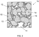
- Figure 3 illustrates another zoomed in view of the arbitrary region 1z of Figure 1 , again in cross-section.
- a noble metal such as one of Pt, Pd, Ir
- Adding in this context may preferably encompasses doping the metal oxide material by the noble metal and / or impregnating the metal oxide material by the noble metal.
- the noble metal may also appear within MOX NPs, while in the latter variant, the noble metal rather only deposits on the surfaces of the MOX NPs.
- noble metal particles 13 are positioned on the surface of the MOX NPs 14.
- the noble metal particles 13 serve as nuclei for the material of the coating 12 during the CVD process, and hence act as support for the coating process.
- the result after coating is illustrated in Figure 3 :
- the coating 12 coats the network of monocrystalline MOC NPs including the noble metal particles 13 on the surfaces of the MOX NPs.
- FIG. 4 illustrates a resistive metal oxide gas sensor according to another embodiment of the present invention.
- the gas sensor comprises a support structure which presently includes a structured substrate 5, e.g., of silicon.
- the substrate 5 has a membrane configuration, i.e., the substrate 5 includes a recess 51 for providing a thinned portion of the substrate 5, on which electrodes 2 are arranged.
- a heater 3 is provided in the thinned portion 51 for heating a porous sensing layer 1 arranged on top of the thinned portion 51 of the substrate 5.
- the electrodes 2 are arranged on or in the gas sensor, so as to be in electrical communication with a porous sensing layer 1. They may be formed out of a platinum or gold layer, which metals are well suited for forming stable electrodes.
- the electrodes 2 may for instance be in an interdigitated configuration containing interdigitated fingers 21.
- the porous sensing layer 1 may advantageously have shape that spans a region that covers or includes the interdigitated fingers 21 of the electrodes 2 to ensure proper electrical communication therewith.
- the heater 3 is in thermal communication with the porous sensing layer 1, to operate the metal oxide material at a target temperature.
- the heater 3 is a resistive heating element.
- a heater 3 of tungsten i.e., a heater 3 comprising at least 50% ( ⁇ 1%), in particular at least 90% ( ⁇ 1%), of tungsten, to best withstand high temperatures.
- Several heaters may be provided, to heat the membrane, or a bridge, see Figure 6 , on which the porous sensing layer 1 is arranged.
- the heater 3 may be embodied as a hotplate, which is resistively heated, without additional resistive elements being needed.
- the heater 3 can be used to heat the porous sensing layer 1 and, if necessary, to furthermore control the temperature of the porous sensing layer 1. Thus, no additional temperature sensors need necessarily be provided.
- the porous sensing layer 1 extends on an exposed surface of the thinned portion 51 of the substrate 2, i.e., the membrane, thereby covering the electrodes 2 to a large part.
- the porous sensing layer 2 may for instance have a disk, ovoid or, still, a rectangular shape. All other properties of the porous sensing layer 1 can be taken from the description of Figures 1 to 3 .
- the gas sensor preferably includes circuitry (integrated therewith), which is electrically connected to the heater 3 and to the electrodes 2.
- the circuitry preferably forms a controller 6 to heat the heater 3 and perform resistive measurements, i.e., to measure an electrical conductivity and/or resistivity of the porous sensing layer 1 by means of the electrodes 2 that are electrically connected to the controller 6.
- a gas sensor according to another embodiment is shown in top view, i.e., a multi-pixel gas.
- a recess or opening 55 is arranged in the substrate 5, preferably silicon substrate.
- a bridge structure 56 extends over the recess or opening 55 and is anchored in the substrate 5.
- the bridge structure 56 includes individual bridges 52, 53, 54 spanning this opening or recess 55.
- Each bridge 52, 53, 54 comprises a central region 57 forming a hotplate 58 and two arms 59 extending between the central region 57 and the substrate 5, thereby suspending the hotplate 58 over the recess or opening 55.
- Each of the bridge structures 56 forms a thin structure with a hotplate.
- the thermal conductance between the hotplate and the substrate 5 is reduced, thus allowing high temperatures to be achieved at low operating power. Further, the thermal mass is reduced, which allows to vary the temperature of the hotplate quickly.
- the gas sensor comprises a set of sensing layers 1, 1a and 1b electrically separated from each other.
- Each sensing layer 1, 1a, 1b is arranged on a dedicated hotplate 58.
- Each of the sensing layers 1, 1a and 1b comprises a MOX material.
- the MOX material changes at least one electrical property as a function of the composition of the gas reaching it. The change of the property can be measured in order to obtain information on said composition.
- At least one of the sensing layers is the porous sensing layer 1 as introduced in the previous embodiments, while the other sensing layers 1a, 1b may, for instance, also show different properties as to the presence, the absence, the property of a coating, the porosity, a thickness, the material etc.
- the sensing layers 1a, 1b may, for instance, also show different properties as to the presence, the absence, the property of a coating, the porosity, a thickness, the material etc.
- each of the sensing layers 1, 1a, 1b is in electrical communication with a subset of electrodes, which are not visible in FIG. 6 .
- one or more heaters are in thermal communication with the porous sensing layers 1, 1a, 1b.
- the substrate 5 carries an integrated CMOS circuitry contributing to a controller 6, e.g., including circuitry for driving heaters and processing signals from the electrodes and temperature sensors if any.
- the processing circuitry 6 is integrated in CMOS technology since the whole device described in this section preferably is compatible with current CMOS manufacturing processes.
- FIG. 7 proves the sensitivity to the target gas hydrogen and the absence of cross-sensitivity to typical reducing gases
- FIG. 8 proves the absence of cross-sensitivity to a typical oxidizing gas
- FIG. 9 proves the sensitivity to the target gas ozone
- FIG. 10 proves the long-term stability.
- FIG. 7 shows, in the upper chart, the resistances of a porous sensing layer of a gas sensor according to said given embodiment, after a sequential exposure to concentrations of various gas molecules over time in a gas mixing system, see lower chart.
- the gas molecules the gas sensor was exposed to are in the order as depicted in the chart: hydrogen, ethanol, acetone, toluene, cyclohexane and carbon monoxide in a carrier gas of humidified zero-air.
- the upper chart showing the resistance of the corresponding porous gas sensing layer when exposed to the various gases, only the exposure to hydrogen shows a significant response in the sensing signal taken by the electrodes, i.e., an increase in the electrical conductivity.
- the exposure of the same gas sensor to the other gases does not lead to any significant change in the sensing signal.
- the selectivity of hydrogen versus the other gases is more than 100:1, meaning that when exposed to a given concentration, hydrogen effects a bigger change in the resistance of the porous sensing layer represented by the sensing signal than when exposed to a hundredfold increased concentration of any of the other gases listed.
- the dashed line shows that 0.3ppm of hydrogen effect a larger signal (more resistance drop) than 30ppm of any of the other gases.
- a cross-sensitivity to the other reducing gases is thus designed to be very low.
- the resistance measured in the upper chart of roughly 700 kOhm rather stems from the continuous background concentration of H2 in the gas mixing system, i.e., 0.5 ppm (see FIG. 7 for the same resistance level at 0.5 ppm H2).
- the upper chart of FIG. 9 shows the resistances of the same sample as in FIG. 7 and FIG. 8 , after an exposure to various concentrations of ozone over time in a carrier gas of humidified zero-air and 0.5 ppm hydrogen, see lower chart.
- the ozone concentrations of the lower chart were measured by a UV-optical reference device.
- the present gas sensor is sensitive to ozone and shows fast reaction times.
- the present gas sensor has a limit of detection of much less than 20 ppb ozone in view of the stepwise increase of ozone in the atmosphere around the gas sensor of around 20 ppb, which perfectly are reflected in the change of resistance of the porous sensing layer.
- FIG. 10 shows a plot representing an outdoor field measurement of ozone measured by a calibrated gas sensor according to that same given embodiment as used for FIGs. 7 to 9 .
- the time period shown corresponds to a period of 24 hours, taken six months after the gas sensor was calibrated in a gas mixing system with humidified zero air and 0.5 ppm hydrogen and ozone steps such as shown in FIG. 9 .
- the gas sensor was randomly switched on and off with a duty cycle of roughly 50%.
- the grey signal in the 24-hour measurement represents a continuous monitoring by a UV-optical reference device of the actual ozone concentration, while the dark line represents the ozone concentration measured by the gas sensor, after randomly switching on the gas sensor four times for a random duration. Every time after switching on the gas sensor, the sensing signal quickly supplies the correct ozone concentration present at that point in time and follows any subsequent variation of the concentration of ozone. Hence, the gas sensor is proven as long term stable.
- the invention can further be embodied as a method of operating a resistive MOX gas sensor.
- a porous sensing layer 1 is heated to an operating temperature, step S10, FIG. 11 .
- values indicative of an electrical conductivity of the porous sensing layer are determined (step S50), e.g., thanks to an evaluation unit), and based on signals received S40 from the electrodes.
- Steps S40, S50 may be continuously (i.e., repeatedly) performed, while heating the coated patch.
- the porous sensing layer is preferably heated to a temperature that is between 400 °C and 600 °C.
- a temperature of the coated patch at a desired value. This can notably be achieved thanks to a feedback loop mechanism. This, of course, does not preclude the possibility to occasionally heat the sensor for shorter periods to the target temperature, i.e., intermittent heating.
Landscapes
- Chemical & Material Sciences (AREA)
- Engineering & Computer Science (AREA)
- Health & Medical Sciences (AREA)
- Life Sciences & Earth Sciences (AREA)
- Chemical Kinetics & Catalysis (AREA)
- Immunology (AREA)
- Analytical Chemistry (AREA)
- Pathology (AREA)
- General Physics & Mathematics (AREA)
- General Health & Medical Sciences (AREA)
- Biochemistry (AREA)
- Physics & Mathematics (AREA)
- Inorganic Chemistry (AREA)
- General Chemical & Material Sciences (AREA)
- Materials Engineering (AREA)
- Organic Chemistry (AREA)
- Mechanical Engineering (AREA)
- Metallurgy (AREA)
- Electrochemistry (AREA)
- Nanotechnology (AREA)
- Combustion & Propulsion (AREA)
- Food Science & Technology (AREA)
- Medicinal Chemistry (AREA)
- Investigating Or Analyzing Materials By The Use Of Fluid Adsorption Or Reactions (AREA)
Priority Applications (5)
| Application Number | Priority Date | Filing Date | Title |
|---|---|---|---|
| EP19161038.5A EP3705879A1 (fr) | 2019-03-06 | 2019-03-06 | Capteur de gaz à oxyde métallique résistif |
| PCT/EP2019/076820 WO2020177884A1 (fr) | 2019-03-06 | 2019-10-03 | Capteur de gaz à oxyde métallique résistif et système de surveillance de batterie |
| CN202080018923.3A CN113544499A (zh) | 2019-03-06 | 2020-02-28 | 电阻式金属氧化物气体传感器及其制造方法和操作该传感器的方法 |
| US17/434,908 US20220163473A1 (en) | 2019-03-06 | 2020-02-28 | Resisistive metal oxide gas sensor, manufacturing method thereof and method for operating the sensor |
| PCT/EP2020/055364 WO2020178203A1 (fr) | 2019-03-06 | 2020-02-28 | Capteur de gaz à oxyde métallique résistif, procédé de fabrication correspondant et procédé de fonctionnement du capteur |
Applications Claiming Priority (1)
| Application Number | Priority Date | Filing Date | Title |
|---|---|---|---|
| EP19161038.5A EP3705879A1 (fr) | 2019-03-06 | 2019-03-06 | Capteur de gaz à oxyde métallique résistif |
Publications (1)
| Publication Number | Publication Date |
|---|---|
| EP3705879A1 true EP3705879A1 (fr) | 2020-09-09 |
Family
ID=65717901
Family Applications (1)
| Application Number | Title | Priority Date | Filing Date |
|---|---|---|---|
| EP19161038.5A Withdrawn EP3705879A1 (fr) | 2019-03-06 | 2019-03-06 | Capteur de gaz à oxyde métallique résistif |
Country Status (4)
| Country | Link |
|---|---|
| US (1) | US20220163473A1 (fr) |
| EP (1) | EP3705879A1 (fr) |
| CN (1) | CN113544499A (fr) |
| WO (2) | WO2020177884A1 (fr) |
Families Citing this family (5)
| Publication number | Priority date | Publication date | Assignee | Title |
|---|---|---|---|---|
| US11719660B1 (en) * | 2019-11-15 | 2023-08-08 | United States Of America As Represented By The Administrator Of Nasa | Solid state carbon dioxide sensor |
| AU2021372557A1 (en) * | 2020-10-30 | 2023-06-08 | Royal Melbourne Institute Of Technology | A chemiresistive substrate for a hydrogen gas sensor |
| US20230077000A1 (en) * | 2021-09-07 | 2023-03-09 | Conmed Corporation | Gas concentration measurement in gas sealed trocars |
| CN116380994B (zh) * | 2023-02-23 | 2025-08-19 | 艾感科技(广东)有限公司 | 一种基于单通多孔基底的半导体气体传感器 |
| IT202400003922A1 (it) | 2024-02-23 | 2025-08-23 | Fond Bruno Kessler | Sensore di gas a stato solido e corrispondente procedimento di fabbricazione |
Citations (5)
| Publication number | Priority date | Publication date | Assignee | Title |
|---|---|---|---|---|
| US5624640A (en) * | 1993-10-12 | 1997-04-29 | Robert Bosch Gmbh | Sensor for detecting nitrogen oxide |
| US6012327A (en) * | 1996-05-10 | 2000-01-11 | Siemens Aktiengesellschaft | Gas sensor and method for manufacturing the same |
| US20170167999A1 (en) * | 2015-12-11 | 2017-06-15 | Rohm Co., Ltd. | Semiconductor type gas sensor, method of manufacturing semiconductor type gas sensor, and sensor network system |
| WO2018053655A1 (fr) | 2016-09-21 | 2018-03-29 | Sensirion Ag | Capteur de gaz à oxyde métallique résistif revêtu d'un filtre en fluoropolymère |
| US20190033243A1 (en) * | 2017-07-28 | 2019-01-31 | Apple Inc. | Oxide barrier coated semiconductor gas sensors |
Family Cites Families (16)
| Publication number | Priority date | Publication date | Assignee | Title |
|---|---|---|---|---|
| JP3276288B2 (ja) * | 1996-03-19 | 2002-04-22 | 勝夫 江原 | リチウム電池からのリーク検出方法とその装置 |
| US7648927B2 (en) * | 2005-06-21 | 2010-01-19 | Applied Materials, Inc. | Method for forming silicon-containing materials during a photoexcitation deposition process |
| KR100825765B1 (ko) * | 2006-12-05 | 2008-04-29 | 한국전자통신연구원 | 산화물계 나노 구조물의 제조 방법 |
| EP2105734B1 (fr) * | 2008-03-26 | 2013-11-20 | Micronas GmbH | Capteur de gaz |
| US8028561B2 (en) * | 2008-09-30 | 2011-10-04 | Qualitrol Company, Llc | Hydrogen sensor with air access |
| KR101125170B1 (ko) * | 2009-04-30 | 2012-03-19 | 한국과학기술연구원 | 금속산화물 나노입자를 이용한 가스센서 및 그 제조방법 |
| US8711356B2 (en) * | 2010-02-25 | 2014-04-29 | Stichting Imec Nederland | Gas sensor with a porous layer that detectably affects a surface lattice resonant condition of a nanoparticle array |
| US11624115B2 (en) * | 2010-05-12 | 2023-04-11 | Sio2 Medical Products, Inc. | Syringe with PECVD lubrication |
| JP2013170092A (ja) * | 2012-02-20 | 2013-09-02 | National Institute For Materials Science | 単結晶酸化すずワイヤ |
| EP2762867B1 (fr) * | 2013-01-31 | 2018-11-21 | Sensirion AG | Capteur de gaz avec régulation de température |
| EP3063791B1 (fr) * | 2013-10-30 | 2018-05-30 | Robert Bosch GmbH | Procédé permettant de former un capteur semi-conducteur à base d'oxyde métallique à l'aide d'un dépôt de couches atomiques et capteur semi-conducteur à base d'oxyde métallique correspondant |
| CN105158297A (zh) * | 2015-09-24 | 2015-12-16 | 雷鸣 | 一种mems金属氧化物半导体气体传感器及其制造方法 |
| CN105606661B (zh) * | 2016-03-09 | 2019-02-12 | 中国科学院微电子研究所 | 集成纳米结构的薄膜型mos气体传感器及其制作方法 |
| CN106198644A (zh) * | 2016-06-24 | 2016-12-07 | 苏州纳格光电科技有限公司 | 一种半导体气体传感器及其制备方法 |
| US10877011B2 (en) * | 2016-06-29 | 2020-12-29 | Nexceris, Llc | Systems and methods for monitoring for a gas analyte |
| CN109283227A (zh) * | 2017-07-21 | 2019-01-29 | 苹果公司 | 化学稳健的微型气体传感器 |
-
2019
- 2019-03-06 EP EP19161038.5A patent/EP3705879A1/fr not_active Withdrawn
- 2019-10-03 WO PCT/EP2019/076820 patent/WO2020177884A1/fr not_active Ceased
-
2020
- 2020-02-28 WO PCT/EP2020/055364 patent/WO2020178203A1/fr not_active Ceased
- 2020-02-28 US US17/434,908 patent/US20220163473A1/en not_active Abandoned
- 2020-02-28 CN CN202080018923.3A patent/CN113544499A/zh active Pending
Patent Citations (5)
| Publication number | Priority date | Publication date | Assignee | Title |
|---|---|---|---|---|
| US5624640A (en) * | 1993-10-12 | 1997-04-29 | Robert Bosch Gmbh | Sensor for detecting nitrogen oxide |
| US6012327A (en) * | 1996-05-10 | 2000-01-11 | Siemens Aktiengesellschaft | Gas sensor and method for manufacturing the same |
| US20170167999A1 (en) * | 2015-12-11 | 2017-06-15 | Rohm Co., Ltd. | Semiconductor type gas sensor, method of manufacturing semiconductor type gas sensor, and sensor network system |
| WO2018053655A1 (fr) | 2016-09-21 | 2018-03-29 | Sensirion Ag | Capteur de gaz à oxyde métallique résistif revêtu d'un filtre en fluoropolymère |
| US20190033243A1 (en) * | 2017-07-28 | 2019-01-31 | Apple Inc. | Oxide barrier coated semiconductor gas sensors |
Non-Patent Citations (1)
| Title |
|---|
| FLEISCHER M ET AL: "A SELECTIVE H2 SENSOR IMPLEMENTED USING GA2O3 THIN-FILMS WHICH ARE COVERED WITH A GAS-FILTERING SIO2 LAYER", SENSORS AND ACTUATORS B: CHEMICAL: INTERNATIONAL JOURNAL DEVOTED TO RESEARCH AND DEVELOPMENT OF PHYSICAL AND CHEMICAL TRANSDUCERS, ELSEVIER BV, NL, vol. B36, no. 1/02/03, 1 October 1996 (1996-10-01), pages 297 - 302, XP000681227, ISSN: 0925-4005, DOI: 10.1016/S0925-4005(97)80085-8 * |
Also Published As
| Publication number | Publication date |
|---|---|
| US20220163473A1 (en) | 2022-05-26 |
| WO2020177884A1 (fr) | 2020-09-10 |
| WO2020178203A1 (fr) | 2020-09-10 |
| CN113544499A (zh) | 2021-10-22 |
Similar Documents
| Publication | Publication Date | Title |
|---|---|---|
| US20220163473A1 (en) | Resisistive metal oxide gas sensor, manufacturing method thereof and method for operating the sensor | |
| Sharma et al. | Sensitive, selective and stable tin dioxide thin-films for carbon monoxide and hydrogen sensing in integrated gas sensor array applications | |
| EP3516381B1 (fr) | Capteur resistif a oxide de metal avec une couche filtre en fluoropolymere | |
| EP2044424B1 (fr) | Procédé pour fabriquer un détecteur de gaz présentant des nanostructures d'oxyde de zinc | |
| Mandayo et al. | Strategies to enhance the carbon monoxide sensitivity of tin oxide thin films | |
| EP3786627B1 (fr) | Élément de détection de gaz à semi-conducteur de type mems | |
| EP0488503A2 (fr) | Détecteur de gaz | |
| Schierbaum et al. | Specific palladium and platinum doping for SnO2-based thin film sensor arrays | |
| WO2007122287A1 (fr) | Capteur de gaz semi-conducteur pour microplaque chauffante | |
| WO1996038863A1 (fr) | Capteur chimique utilisant une electrode chimiquement sensible en combinaison avec de minces couches de diamant | |
| Raza et al. | SnO2‐SiO2 1D Core‐Shell Nanowires Heterostructures for Selective Hydrogen Sensing | |
| Ivanov et al. | On the effects of the materials and the noble metal additives to NO2 detection | |
| Kohl | Semiconductor and calorimetric sensor devices and arrays | |
| Sulz et al. | Ni, In and Sb implanted Pt and V catalysed thin-film SnO2 gas sensors | |
| Reisert et al. | Multi‐sensor chip for the investigation of different types of metal oxides for the detection of H2 O 2 in the ppm range | |
| Liu et al. | A low power bridge-type gas sensor with enhanced sensitivity to ethanol by sandwiched ZnO/Au/ZnO film sputtered in O₂ atmosphere | |
| Patel et al. | Film structure and conductometric hydrogen-gas-sensing characteristics of ultrathin platinum films | |
| Hahn | SnO2 thick film sensors at ultimate limits: Performance at low O2 and H2O concentrations; Size reduction by CMOS technology | |
| Abadi et al. | Characterization of mixed xWO3 (1-x) Y2O3 Nanoparticle thick film for gas sensing application | |
| Mandayo | Gas detection by semiconductor ceramics: tin oxide as improved sensing material | |
| AU2003225026A1 (en) | Method for restoring the sensitivity, speed or stability of a gas-sensitive material | |
| US20230358704A1 (en) | Method for manufacturing an electrochemical gas sensor | |
| RU2403563C1 (ru) | Дифференциальный сенсорный датчик для газоанализатора | |
| Epifani et al. | Hall effect measurements in gas sensors based on nanosized Os-doped sol-gel derived SnO 2 thin films | |
| Wöllenstein et al. | Gas sensitive behaviour and morphology of reactive evaporated V2O5 thin films |
Legal Events
| Date | Code | Title | Description |
|---|---|---|---|
| PUAI | Public reference made under article 153(3) epc to a published international application that has entered the european phase |
Free format text: ORIGINAL CODE: 0009012 |
|
| STAA | Information on the status of an ep patent application or granted ep patent |
Free format text: STATUS: THE APPLICATION HAS BEEN PUBLISHED |
|
| AK | Designated contracting states |
Kind code of ref document: A1 Designated state(s): AL AT BE BG CH CY CZ DE DK EE ES FI FR GB GR HR HU IE IS IT LI LT LU LV MC MK MT NL NO PL PT RO RS SE SI SK SM TR |
|
| AX | Request for extension of the european patent |
Extension state: BA ME |
|
| STAA | Information on the status of an ep patent application or granted ep patent |
Free format text: STATUS: REQUEST FOR EXAMINATION WAS MADE |
|
| 17P | Request for examination filed |
Effective date: 20210308 |
|
| RBV | Designated contracting states (corrected) |
Designated state(s): AL AT BE BG CH CY CZ DE DK EE ES FI FR GB GR HR HU IE IS IT LI LT LU LV MC MK MT NL NO PL PT RO RS SE SI SK SM TR |
|
| GRAP | Despatch of communication of intention to grant a patent |
Free format text: ORIGINAL CODE: EPIDOSNIGR1 |
|
| STAA | Information on the status of an ep patent application or granted ep patent |
Free format text: STATUS: GRANT OF PATENT IS INTENDED |
|
| INTG | Intention to grant announced |
Effective date: 20221104 |
|
| STAA | Information on the status of an ep patent application or granted ep patent |
Free format text: STATUS: THE APPLICATION IS DEEMED TO BE WITHDRAWN |
|
| 18D | Application deemed to be withdrawn |
Effective date: 20230315 |