EP3709632A1 - Circuit de lecture, étape de lecture, capteur d'image, dispositif électronique et procédé de lecture d'un capteur d'image - Google Patents
Circuit de lecture, étape de lecture, capteur d'image, dispositif électronique et procédé de lecture d'un capteur d'image Download PDFInfo
- Publication number
- EP3709632A1 EP3709632A1 EP19162296.8A EP19162296A EP3709632A1 EP 3709632 A1 EP3709632 A1 EP 3709632A1 EP 19162296 A EP19162296 A EP 19162296A EP 3709632 A1 EP3709632 A1 EP 3709632A1
- Authority
- EP
- European Patent Office
- Prior art keywords
- sample
- sampling
- pixel
- readout
- hold element
- Prior art date
- Legal status (The legal status is an assumption and is not a legal conclusion. Google has not performed a legal analysis and makes no representation as to the accuracy of the status listed.)
- Granted
Links
Images


Classifications
-
- H—ELECTRICITY
- H04—ELECTRIC COMMUNICATION TECHNIQUE
- H04N—PICTORIAL COMMUNICATION, e.g. TELEVISION
- H04N25/00—Circuitry of solid-state image sensors [SSIS]; Control thereof
- H04N25/70—SSIS architectures; Circuits associated therewith
- H04N25/76—Addressed sensors, e.g. MOS or CMOS sensors
- H04N25/78—Readout circuits for addressed sensors, e.g. output amplifiers or A/D converters
-
- H—ELECTRICITY
- H04—ELECTRIC COMMUNICATION TECHNIQUE
- H04N—PICTORIAL COMMUNICATION, e.g. TELEVISION
- H04N25/00—Circuitry of solid-state image sensors [SSIS]; Control thereof
-
- H—ELECTRICITY
- H04—ELECTRIC COMMUNICATION TECHNIQUE
- H04N—PICTORIAL COMMUNICATION, e.g. TELEVISION
- H04N25/00—Circuitry of solid-state image sensors [SSIS]; Control thereof
- H04N25/70—SSIS architectures; Circuits associated therewith
- H04N25/76—Addressed sensors, e.g. MOS or CMOS sensors
Definitions
- the present disclosure relates to a readout circuit, to a readout stage with such readout circuit, to an image sensor with such a readout circuit, to an electronic device with a camera system comprising such an image sensor and to a method for reading out an image sensor.
- Image sensors for example CMOS image sensors, CIS, usually comprise an array of unit elements, called pixels.
- the array of pixels is exposed to radiation during an exposure period and, subsequently, the signal value of each pixel is read from the array.
- the pixels and readout circuitry often introduce random noise in the image, an unwanted side-product of image capture.
- the readout occurs during two phases. These two readout phases correspond to two different signal levels typically called the “reset” level and the actual “signal” level. By subtracting these two signal levels, any common mode noise, as well as some low frequency noise (1/f noise), between them can be eliminated. This is called correlated double sampling, CDS. For low noise image capture, CDS is widely used.
- ADC analog-to digital converter
- Ramp based ADCs are widely used in CIS.
- the signal level and a linearly sloping ramp signal are applied to a comparator and a counter starts counting at the start of the conversion phase.
- the comparator toggles and the value of the counter is latched into a memory.
- the larger the voltage range of the input signal the longer the conversion takes.
- the reset level can show a large variation, e.g. due to variations of the pixel transistors. A large variation in the reset level will require a longer ramping phase to convert the reset level. This will increase the conversion time of the ADC and reduce the frame rate of the image sensor.
- PGA programmable gain amplifiers
- An object to be achieved is to provide an improved signal processing concept for reading out a pixel array of an image sensor with improved performance.
- a pixel array may have a multitude of pixels organized in a structure with one or more pixel groups, e.g. pixel columns, to form a linear image sensor or a two-dimensional image sensor. The grouping can be made column by column, row by row or according to other criteria, e.g. to form sub-arrays.
- each of the pixels comprises a photodiode and a pixel buffer, for example a source follower, coupled to the photodiode.
- a so-called floating diffusion is present at the input of the pixel buffer.
- a transfer gate may or may not be foreseen between the photodiode and the pixel buffer.
- An output of the pixel buffer often corresponds to an output of the respective pixel.
- a pixel array comprises at least one pixel group, e.g. pixel column, with a plurality of pixels connected to a group bus or column bus, to which a readout circuit can be connected.
- the improved signal processing concept is based on the idea that for each pixel group of an image sensor, a sampling structure with two or more sample-and-hold elements is provided in a respective readout circuit that allows pipelined readout and sampling of the pixels of the pixel group, e.g. pixel column.
- the sampling structure further includes a bypass switch connecting the input and the output of the sampling structure. This way a signal received from the pixel group can be directly transferred to a charge store connected between the output of the sampling structure and a signal output that is connectable to an input of an analog-to-digital converter, ADC.
- the terminals of the charge store are connected to respective reference terminals to which respective reference voltages can be provided.
- This allows, together with the bypass switch, to provide a defined reset level to the ADC, which in turn can reduce a sensitivity to the variations of the transistors in the pixel and further reduce the conversion time of the ADC. Furthermore a sensitivity to other variations in the pixels like reference voltages, e.g. used as reset level, may be reduced.
- the same readout structure can be employed for each pixel group, e.g. pixel column, of a multi-group or multi-column pixel array.
- respective single voltage buffers for providing the one or two respective reference voltages may be sufficient for the whole pixel array, such that both area and power consumption can be reduced.
- a readout circuit for an image sensor having a pixel array comprising at least one pixel group, e.g. pixel column, with a plurality of pixels connected to a group bus or column bus.
- the readout circuit comprises a group input or column input for connecting to the group bus or column bus and a signal output for connecting to an input of an analog-to-digital converter, ADC.
- the readout circuit further comprises a first reference terminal for receiving a first reference voltage and a second reference terminal for receiving a second reference voltage.
- a sampling bank of the readout circuit comprises a first sample-and-hold element and an at least second sample-and-hold element coupled between the column input and an output of the sampling bank.
- the sampling bank further comprises a bypass switch connected between the column input and the output of the sampling bank, e.g. in parallel to the first and the at least second sample-and-hold element.
- a charge store is connected between the output of the sampling bank and the signal output.
- a first charge switch is connected between the first reference terminal and the signal output and a second charge switch is connected between a second reference terminal and the output of the sampling bank.
- sample-and-hold elements in the sampling bank allows pipelined sampling and readout of the respective voltage levels of the pixels of the pixel group.
- the bypass switch together with the charge store and the reference voltages allows providing defined signal levels at the signal output, in particular a defined reset level.
- both terminals of the charge store can be individually charged with the respective reference voltages, defined conditions when reading out the signal level of the pixel can be established.
- the structure of the readout circuit allows to perform a controlled sampling and readout of the respective signal levels received from the pixels via the group bus, respectively group input, and further allows to ensure well-defined signal levels being provided at the signal output for processing with an ADC.
- the readout circuit is configured, during a sample phase, which may be a first sample phase, to sample a reset level voltage and a signal level voltage received, e.g. consecutively received, at the group input from one of the pixels of the at least one pixel group, employing the first sample-and-hold element and the at least second sample-and-hold element. It can be chosen arbitrarily whether first the reset level or first the signal level is sampled.
- the readout circuit is further configured, during a calibration phase, to close the bypass switch and to connect the signal output to the first reference terminal employing the first charge switch. For example, this allows to charge the charge store with a voltage corresponding to a difference between the first reference voltage and the voltage level provided from the pixel.
- the reset level voltage is provided from the pixel at the group input and hence to the output of the sampling bank, respectively the connected charge store.
- the readout circuit is further configured, during a readout phase, which may be a first readout phase, to read out, for example consecutively read out, the sampled reset level voltage and the sampled signal level voltage from the first sample-and-hold element and the at least second sample-and-hold element.
- a readout phase which may be a first readout phase
- the sequential order of reading out the sampled voltages can be chosen arbitrarily and can differ from the sequence, with which the voltage levels had been sampled during the sampling phase. Hence, a flexible pipelining can be achieved.
- accuracy of the read out voltages, respectively the voltages provided at the signal output can be increased.
- the readout circuit may be configured, during the first readout phase, to connect the output of the sampling bank to the second reference terminal employing the second charge switch for a predetermined time before the readout of the sampled reset level voltage and before the readout of the sampled signal level voltage. For example, the connection is made before each of the single readout processes.
- a charge distribution between a storage element of the respective sample-and-hold element and the charge store downstream of the sampling bank starts with defined conditions, further increasing the accuracy of the read out signals.
- the pixels of such a pixel column are usually organized as a plurality of rows such that the pixel array is formed of the at least one pixel column and a plurality of rows.
- sampling bank comprises two sample-and-hold elements, as comprised by the examples described above, pipelining of reset level and signal level of the pixel of a single row can be performed. However, if a third and a fourth sample-and-hold element are provided in the sampling bank, pipelined operation for two rows is possible. Pipelining is also applicable to other forms of pixel groups, which should be apparent to the skilled reader.
- the sampling bank further comprises a third sample-and-hold element and a fourth sample-and-hold element, connected in parallel to the first and the second sample-and-hold elements.
- a reset level and a signal level of one row can be sampled with two of the four sample-and-hold elements, previously stored voltage levels can be read out from the other two sample-and-hold elements.
- the readout circuit may be further configured, during a second readout phase, which at least partially is overlapping with the first sampling phase, to read out, for example consecutively read out, a previously sampled reset level voltage and a previously sampled signal level voltage from the third sample-and-hold element and the fourth sample-and-hold element. It should be noted that an exact synchronization between the sampling process of the first sampling phase and the readout process of the second readout phase is not required.
- the readout circuit is further configured, during a second sampling phase, which at least partially is overlapping with the first readout phase, to sample a further reset level voltage and a further signal level voltage and a further signal level voltage received, for example consecutively received, at the column input from a further one of the pixels of the at least one pixel group, employing the third sample-and-hold element and the fourth sample-and-hold element.
- the further one of the pixels of the pixel array is associated with a different row of the group compared to the pixel sampled during the first sampling phase.
- control signals can be generated by respective control circuitry that may be part of the readout circuit or that may be external to the readout circuit and for example common to several readout circuits associated with different pixel groups of the pixel array.
- the first sample-and-hold element and the at least second sample-and-hold element are connected in parallel to each other and to the bypass switch between the group input and the output of the sampling bank. Moreover, if an implementation with a third and a fourth sample-and-hold element is chosen, these can each be connected in parallel to the first and the second sample-and-hold element, and consequently, to the bypass switch.
- the first sample-and-hold element and the at least second sample-and-hold element form a cascade that is connected between the group input and the output of the sampling bank in parallel to the bypass switch.
- these may form another cascade, that is connected between the group input and the output of the sampling bank in parallel to the cascade of the first and the second sample-and-hold element, and consequently, to the bypass switch.
- the improved signal processing concept can be further implemented in a readout stage for an image sensor having a pixel array with at least two pixel groups, e.g. pixel columns, where each pixel group with a plurality of pixels is connected to a respectively associated group bus of that pixel group.
- the readout stage comprises, for each of the pixel groups, an associated readout circuit according to one of the implementations described above, having its group input connected to the associated group bus.
- such a readout stage may further comprise one or two voltage buffers for connecting to the respective reference terminals of each of the readout circuits.
- the readout stage comprises a first voltage buffer for providing a first reference voltage, wherein an output of the first voltage buffer is connected to the respective first reference terminals of each of the readout circuits.
- the readout stage may further comprise a second voltage buffer for providing the second reference voltage, wherein an output of the second voltage buffer is connected to the respective second reference terminals of each of the readout circuits.
- this voltage buffer can be connected to both the first and the second reference terminals of the readout circuits, such that the same reference voltage is present at both terminals. Still a controlled provision of respective signal levels at the signal outputs of the readout circuits is possible. If two buffers with two different reference voltages are provided, the respective voltage levels can be adapted more flexibly.
- the readout stage includes a greater number of voltage buffers, each of the voltage buffers providing the respective reference voltage to several readout circuits together.
- each of the voltage buffers providing the respective reference voltage to several readout circuits together.
- the improved signal processing concept also proposes an image sensor comprising a pixel array with at least two pixel groups, e.g. pixel columns, each pixel group with a plurality of pixels connected to a respectively associated group bus of that pixel group and further comprising, for each of the pixel groups, an associated readout circuit according to one of the implementations described above and having its group input connected to the associated group bus.
- the image sensor may further comprise a first and/or a second voltage buffer as described before in conjunction with the implementations of the readout stage.
- the image sensor may comprise the pixel array and a readout stage according to one of the implementations described above.
- the image sensor may further comprise, for each readout circuit, an associated ADC, for example ramp-based ADC, connected to the respective signal output of that readout circuit.
- an associated ADC for example ramp-based ADC
- such ADCs can also be titled “group ADCs” or “column ADCs”.
- An image sensor according to one of the implementations described above can be used in a camera system of various electronic devices, for example.
- Such electronic devices may include smartphones, tablet computers, portable computers and the like, but also larger devices such as personal computers and/or their displays.
- Electronic devices further include photo or video cameras and smart watches and other wearables. Suitable electronic devices further may be devices for machine vision, medical imaging or automotive imaging.
- a method for reading out an image sensor having a pixel array and a readout circuit comprises at least one pixel group, e.g. pixel column, with a plurality of pixels connected to a group bus, and the readout circuit includes a sampling bank comprising a first sample-and-hold element and an at least second sample-and-hold embodiment coupled between the group bus and an output of the sampling bank.
- the readout circuit further comprises a bypass switch connected between the group input and the output of the sampling bank, and a charge store connected between the output of the sampling bank and a signal output.
- the method can be performed with a readout circuit according to one of the implementations described above.
- the method comprises, during a sampling phase, which may be a first sampling phase, sampling a reset level voltage and a signal level voltage received, for example consecutively received, at the group bus from one of the pixels of the at least one pixel group, employing the first sample-and-hold element and the at least second sample-and-hold element.
- the method further comprises, in a calibration phase, closing the bypass switch and providing a reference voltage to the signal output.
- the method further comprises, during a readout phase, which may be a first readout phase, to read out, e.g. consecutively read out, the sampled reset level voltage and the sampled signal level voltage from the first sample-and-hold element and the at least sample-and-hold element.
- the sequence of sampling and reading the signal level voltage and the reset level voltage can be chosen arbitrarily. Due to the parallel connected sample-and-hold elements, for example parallel sampling and reading out is not intended.
- the method further comprises, during the first readout phase, providing the reference voltage or a further reference voltage to the output of the sampling bank for a predetermined time before the readout of the sampled reset level voltage and before the readout of the sampled signal level voltage, e.g. before each readout process.
- the defined reference voltage increases precision in the readout process.
- the reset level voltage is provided to the output of the sampling bank by closing the bypass switch. Hence, the reset level voltage is directly provided without intermediate sampling and reading out with the sample-and-hold elements.
- the method is intended for a configuration, where the sampling bank further comprises a third sample-and-hold element and a fourth sample-and-hold element, connected in parallel to the first and second sample-and-hold element.
- the method further comprises, during a second readout phase, which is at least partially overlapping with the first sampling phase, reading out, e.g. consecutively reading out, a previously sampled reset level voltage and a previously sampled signal level voltage from the third sample-and-hold element and the fourth sample-and-hold element.
- the method includes sampling a further reset level voltage and a further signal level voltage received, e.g.
- signals from two different rows of a pixel group can be processed concurrently or in a pipelined fashion, such that the voltage levels of the pixel of one row are sampled and the voltage levels of a pixel of another row, which have been previously sampled, are read out.
- reading out comprises analog-to-digital conversion of a respective value at the signal output resulting from the respective voltage read out from the respective one of the sample-and-hold elements. It should be noted in this respect that not necessarily the voltage level stored on the sample-and-hold element is converted directly but under the influence of the charge, respectively voltage, of the charge store connected between the sampling bank and the signal output.
- Image sensors for example CMOS image sensors, CIS, regularly include a pixel array with a multitude of pixels organized in one or more pixel groups, e.g. pixel columns, each with a plurality of pixels.
- the array of pixels is exposed to radiation during an exposure period and subsequently the signal value of each pixel is read from the pixel array.
- Figure 1 shows an example detail of an image sensor, in particular one pixel group in form of a pixel column with a plurality of pixels PXL1, PXL2, PXL3, ..., PXLN connected to a group bus or column bus CB1, and a readout circuit RO1 having a group input or column input CI1 connected to the column bus CB1 and a signal output ADCOUT connected to an ADC CADC1.
- the readout circuit RO1 comprises a sampling bank BSH1 being connected to the column input CI1 at its input side and to a charge store C0 at its output side.
- the charge store C0 may be implemented as a capacitor and may be called a feed forward capacitor.
- first terminal of the charge store C0 is connected to the output of the sampling bank BSH1
- second terminal of the charge store C0 is connected to the signal output ADCOUT1.
- a first charge switch SPC1 connects the signal output ADCOUT1 to a first reference terminal VTREF1
- a second charge switch SPC0 connects the output of the sampling bank BSH1 to a second reference terminal VTREF0.
- Respective voltage buffers BUF1, BUF0 can be provided, which provide a first reference voltage VREF1 and a second reference voltage VREF0 to the first reference terminal VTREF1 and the second reference terminal VTREF0, respectively.
- the voltage buffers BUF1, BUF0 are shown as unity gain buffer amplifiers.
- the reference voltages VREF1, VREF0 could be provided to the respective reference terminals VTREF1, VTREF0 from other circuit implementations as well.
- the buffer elements BUF1, BUF0 may be provided only once or at least with only a limited number of actual representations such that the reference voltages for a plurality of readout circuits are provided by the same buffer element.
- the sampling bank BSH1 comprises a first sample-and-hold element SH0 and at least one further sample-and-hold element indicated by the dashed block. Furthermore, a bypass switch BS is connected in parallel to the sample-and-hold elements, i.e. between the group input CI1 and the output of the sampling bank BSH1.
- the illustration of Figure 1 represents an implementation for a single pixel column. While a linear image sensor may have only this single pixel column, 2D image sensors usually have a plurality of pixel columns processed in parallel. Hence, in such an image sensor with several pixel columns, a readout circuit like the readout circuit RO1 shown in Figure 1 , can be provided for each pixel column or any other kind of pixel group. Furthermore, also a dedicated ADC may be provided for each pixel column, connected to the respective signal output of the readout circuit associated with this pixel column.
- FIG. 2A and Figure 2B example implementations of a sampling bank to be used in the readout circuit RO1 of Figure 1 is illustrated, respectively.
- the implementation according to Figure 2A includes two sample-and-hold elements SH0 and SH1, each comprising a sampling capacitor SC0, SC1, a sampling switch SMS0, SMS1 connecting the sampling capacitors SC0, SC1 to an input of the sampling bank, and respective readout switches RES0, RES1 connecting the sampling capacitors SC0, SC1 to the output of the sampling bank.
- the first and the second sample-and-hold element SH0, SH1 are connected in parallel between the input and the output of the sampling bank.
- the bypass switch BS is connected in parallel to both sample-and-hold elements SH0, SH1.
- the sampling bank with two sample-and-hold elements allows pipelined processing of two voltage levels, for example a reset level voltage and a signal level voltage provided by one of the pixels.
- the bypass switch BS allows to provide a voltage level being present at the input side of the sampling bank directly to the output of the sampling bank without intermediate storage. This will be explained in more detail later.
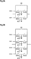
- FIG. 2B the structure of Figure 2A is further equipped with a third and a fourth sample-and-hold element SH2, SH3, which each generally have the same structure as the first two sample-and-hold elements SH0, SH1.
- the third and the fourth sample-and-hold elements SH2, SH3 are also connected in parallel to the sample-and-hold elements SH0, SH1. Accordingly, they feature sampling capacitors SC2, SC3, sampling switches SMS2, SMS3 and readout switches RES2, RES3.
- the two additional sample-and-hold elements SH2, SH3 allow the pipelined processing of four voltage levels, for example reset level voltage and signal level voltage of pixels of two different rows of a column.
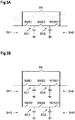
- Figures 3A and 3B show implementations where the two sample-and-hold elements SH0, SH1 form a cascade with the two sampling capacitors SC0, SC1 and associated sampling switches SMS0, SMS1.
- the cascade shares a common readout switch RES0/1.
- the bypass switch BS is connected in parallel to both sample-and-hold elements SH0, SH1, i.e. the cascade.
- the structure of Figure 3A is further equipped with a third and a fourth sample-and-hold element SH2, SH3, which generally have the same structure as the first two sample-and-hold elements SH0, SH1.
- the third and the fourth sample-and-hold elements SH2, SH3 form another cascade with the two sampling capacitors SC2, SC3 and associated sampling switches SMS2, SMS3, sharing a common readout switch RES2/3.
- the sampling bank of Figure 3A with two sample-and-hold elements also allows pipelined processing of two voltage levels, for example a reset level voltage and a signal level voltage provided by one of the pixels.
- the bypass switch BS as describe above, allows to provide a voltage level being present at the input side of the sampling bank directly to the output of the sampling bank without intermediate storage.
- the two additional sample-and-hold elements SH2, SH3 of Figure 3B allow the pipelined processing of four voltage levels, for example reset level voltage and signal level voltage of pixels of two different rows of a column.
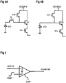
- Each of the pixels comprises a photodiode PD coupled to an input of a source follower SF connected between a pixel supply voltage VDDPIX and an output of the pixel via a respective selection transistor controlled by a selection signal SEL. Furthermore, the input of the source follower SF is connected to the pixel supply voltage VDDPIX by means of a reset transistor controlled by a reset signal RST.
- the photodiode PD While in the pixel of Figure 4A a transfer gate is present between the photodiode and the source follower SF, controlled by a transfer signal TX, the photodiode PD is connected to the source follower SF directly in the pixel implementation of Figure 4B . Due to the number of transistors in the pixel, the pixel of Figure 4A can also be called a 4T pixel while the pixel of Figure 4B can be called a 3T pixel. In the 3T pixel, the signal level voltage is provided to the pixel output by respective control of the reset transistor.
- each pixel is able to provide a reset level voltage and a signal level voltage at the column bus CB1 in response to respective control.
- Figure 5 shows a basic and symbolic representation of a ramp-based ADC as an example ADC to be used at the output of the readout circuit.
- the output of the readout circuit i.e. a respective voltage level ADCIN
- a comparator CMP At a second input of the comparator CMP, a ramp signal RMP is provided. If the ramp signal RMP crosses the input voltage level ADCIN, a counter is triggered, the counter value representing a digital value of the input voltage level.
- Ramp-based ADCs are well known in the art and therefore the counter structure is not shown here for reasons of clarity.
- the improved signal processing concept allows for increasing the frame rate of image sensors using a so-called pipelined readout architecture.
- operations may include CDS, sample-and-hold operations and A-D conversion.
- these operations may take place simultaneously between the readout of the different rows of the pixel column. E.g. while the pixel values of the current row are being stored in the sample-and-hold elements, the values of the previous row are being A-D converted. The slowest operation in the readout of the row will now limit the row time instead of the sum of these operations.
- Pipelining increases the frame rate of the image sensor in this way.
- a feedforward capacitor in form of the charge store C0 is placed between the column input CI1 and the ADC.
- the pixel reset level often has a large variation, if this voltage is fed directly into the ADC, a substantial amount of time would be needed to cover the reset voltage range and this would increase the total conversion time of the ADC. Therefore, charge store C0 is introduced before the signal output ADCOUT1 to block the absolute value of the reset level voltage and the signal level voltage.
- the known reference voltage VREF1 is applied at the signal output ADCOUT1, which serves as the reset level.
- Figure 6 shows an example signal diagram for reading out pixels of a pixel column in a pipelined fashion.
- the signal diagram is not intended to be complete for a whole pixel column but covers only a limited time of the readout process, which is still suitable to understand the whole readout process.
- Figure 6 shows the course of several signals that may be suitable to read out a 4T pixel like that shown in Figure 4A , for example.
- the signal SEL ⁇ i> represents a selection signal for a pixel of a specific row i.
- RST ⁇ i> represents a reset signal for the specific pixel in that row i and
- TX ⁇ i> represents the transfer signal for a pixel in a specific row i.
- the above-mentioned signals SEL ⁇ i>, RST ⁇ i>, TX ⁇ i> could also be represented as two signals each.
- the bypass signal BYP controls the bypass switch BS.
- Charge switch signals PC0, PC1 control the charge switches SPCO, SPC1 respectively.
- the sampling signals SMP ⁇ 0:3> respectively control the sampling switches SMS0, SMS1, SMS2, SMS3.
- the readout signals READ ⁇ 0:3> control the readout switches RES0, RES1, RES2, RES3.
- the next phase corresponds to a calibration phase for the actual row N.
- This scheme will now be explained in more detail.
- Sampling the signal level voltage is finished after the transfer signal TX ⁇ i> goes low.
- the first sampling phase follows a calibration phase during which the reset level voltage from the pixel of the actual row N is directly provided to the left terminal of charge store C0 by means of the signals SEL ⁇ i>, RST ⁇ i> and BYP.
- the switch SPC1 is closed due to the high level of the signal PC1, such that the first reference voltage VREF1 is provided to the right terminal of the charge store C0.
- a first readout phase for the row N starts, during which the previously sampled signals of the sample-and-hold elements SH0, SH1 are read out for being provided to the signal output ADCOUT1.
- the signal PC0 Before activating the readout switches RES0, RES1, respectively, the signal PC0 respectively activates the second charge switch SPC0 for providing the second reference voltage to the left side terminal of the charge store C0.
- the input node of the charge store C0 is recharged to the second reference voltage VREF0 to avoid memory-induced effects on the charge store.
- the timing as shown in Fig. 6 can be varied slightly without changing the described sampling and readout scheme in general. For example, the sampling signals SMP ⁇ i> could be shifted in time such that they go low again before the reset signal RST ⁇ i> or the transfer signal TX ⁇ i>, respectively, go low.
- the reset level voltage is read out first from the first sample-and-hold element SH0, i.e. before the signal level voltage.
- an accurately defined reset level is provided to the signal output ADCOUT1 with this reset level being the reference voltage VREF1. Since VREF1 is independent from variations of the pixel transistors, it will not show or show only small variations across the pixel array. A relatively short ramp in the ADC is sufficient to convert this reset level, thereby reducing the total amount of conversion time.
- the combination of the precharging of the charge store C0 during the calibration phase with the sampled reset level voltage results in the first reference voltage VREF1 being present at the signal output ADCOUT1, respectively the input of the ADC.
- a second sampling phase corresponding to the sampling of voltage levels of a pixel of a next row N+1 is performed.
- the second sampling phase corresponds to, or at least partially overlaps with, the first readout phase.
- the respective pixel control signals SEL ⁇ i>, RST ⁇ i>, TX ⁇ i> are controlling the pixel of the next row N+1 in this case.
- a group of M columns may share the buffered reference voltages VREF1, VREF0.
- M may comprise the total number of columns (chip level).
- the switch SPC1 controlled by PC1 however and the switch SPC0 controlled by PC0 are part of the column readout circuit.
- the bypass switch BS is activated to connect the pixel output, which now again contains the reset level voltage VRST, to the input of charge store C0.
- the comparator is calibrated for the next row, meaning that the input of the comparator is precharged to VREF1 to prepare the ADC for the next conversion.
- Figure 7 shows a signal diagram of several signals controlling the readout process with a pixel according to Figure 4B but still using the readout circuit of Figure 1 with a sampling bank BSH1 with four sample-and-hold elements.
- a single pipelined sampling and readout phase are shown in this diagram which can easily be extended to a full diagram by the skilled person from the disclosure of Figure 6 .
- the signal level voltage is sampled on the first sample-and-hold element SH0 and afterwards the reset level voltage is sampled on the second sample-and-hold element SH1, controlled by the respective sampling signals SMP ⁇ 0> and SMP ⁇ 1>.
- the sampling refers to row N
- the parallel, pipelined readout process refers to the previously sampled row N-1.
- the voltage level signal is read out before the reset level signal.
- the reset level voltage is being read at the end of the row time, respectively the readout phase, such that it does not need to settle anymore, potentially resulting in a speed up or more accurate settling of the calibrated value.
- a calibration phase follows the sampling/readout phase by precharging the charge store C0 as described before in conjunction with Figure 6 .
- the reset level voltage and the associated signal level voltage can be sampled onto one of the cascades.
- the reset level voltage is first sampled onto the "right" sampling capacitors SC0 respectively SC2, employing both sample switches SMS0, SMS1, respectively SMS2, SMS3.
- the signal level voltage can be sampled onto the "left" sampling capacitors SC1 respectively SC3, employing sampling switch SMS1 respectively SMS3.
- Readout is performed accordingly, which should be apparent to the skilled reader.
- sampling and readout can be performed concurrently on different cascades, thereby allowing the pipelined processing of pixels of different rows.
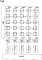
- Figure 8 shows a schematic representation of an image sensor with a pixel array with five pixel columns with respective pixels connected column buses CB1, CB2, CB3, CB4 and CB5.
- Each column comprises five rows of pixels that can be controlled with a row selection RSEL.
- RSEL row selection
- a readout circuit RO1, RO2, RO3, RO4, RO5 having its respective column input CI1, CI2, CI3, CI4, CI5 connected to the column bus CB1, CB2, CB3, CB4, CB5.
- the readout circuits together may form a readout stage.
- the outputs of the readout circuits RO1 to RO5 are connected to respective column ADCs, CADC1, CADC2, CADC3, CADC4, CADC5, the outputs of which are connected to a digital processing block DIG I/O which may further process the converted signal values.
- the readout circuits of such an image sensor may be implemented according to one of the implementations described above, in particular with respect to Figure 1 .
- An image sensor according to one of the implementations described above can be used in camera systems.
- camera systems may be included in various electronic devices.
- Such electronic devices may include smartphones, tablet computers, portable computers and the like, but also larger devices such as personal computers and/or their displays.
- Electronic devices further include photo or video cameras and smart watches and other wearables. Suitable electronic devices further may be devices for machine vision, medical imaging or automotive imaging.
Landscapes
- Engineering & Computer Science (AREA)
- Multimedia (AREA)
- Signal Processing (AREA)
- Transforming Light Signals Into Electric Signals (AREA)
Priority Applications (4)
| Application Number | Priority Date | Filing Date | Title |
|---|---|---|---|
| EP19162296.8A EP3709632B1 (fr) | 2019-03-12 | 2019-03-12 | Circuit de lecture, étape de lecture, capteur d'image, dispositif électronique et procédé de lecture d'un capteur d'image |
| CN202080016149.2A CN113475059B (zh) | 2019-03-12 | 2020-02-05 | 读出电路、读出级、图像传感器、电子设备和用于读出图像传感器的方法 |
| US17/436,249 US11838667B2 (en) | 2019-03-12 | 2020-02-05 | Readout circuit, readout stage, image sensor, electronic device and method for reading out an image sensor |
| PCT/EP2020/052839 WO2020182375A1 (fr) | 2019-03-12 | 2020-02-05 | Circuit de lecture, étape de lecture, capteur d'image, dispositif électronique et procédé de lecture d'un capteur d'image |
Applications Claiming Priority (1)
| Application Number | Priority Date | Filing Date | Title |
|---|---|---|---|
| EP19162296.8A EP3709632B1 (fr) | 2019-03-12 | 2019-03-12 | Circuit de lecture, étape de lecture, capteur d'image, dispositif électronique et procédé de lecture d'un capteur d'image |
Publications (2)
| Publication Number | Publication Date |
|---|---|
| EP3709632A1 true EP3709632A1 (fr) | 2020-09-16 |
| EP3709632B1 EP3709632B1 (fr) | 2021-10-06 |
Family
ID=65801904
Family Applications (1)
| Application Number | Title | Priority Date | Filing Date |
|---|---|---|---|
| EP19162296.8A Active EP3709632B1 (fr) | 2019-03-12 | 2019-03-12 | Circuit de lecture, étape de lecture, capteur d'image, dispositif électronique et procédé de lecture d'un capteur d'image |
Country Status (4)
| Country | Link |
|---|---|
| US (1) | US11838667B2 (fr) |
| EP (1) | EP3709632B1 (fr) |
| CN (1) | CN113475059B (fr) |
| WO (1) | WO2020182375A1 (fr) |
Cited By (1)
| Publication number | Priority date | Publication date | Assignee | Title |
|---|---|---|---|---|
| JPWO2022075119A1 (fr) * | 2020-10-05 | 2022-04-14 |
Families Citing this family (5)
| Publication number | Priority date | Publication date | Assignee | Title |
|---|---|---|---|---|
| CN114173073B (zh) * | 2021-12-06 | 2024-01-23 | 锐芯微电子股份有限公司 | 电路结构及其工作方法 |
| US11894857B2 (en) * | 2022-03-15 | 2024-02-06 | Shanghai United Imaging Microelectronics Technology Co., Ltd. | Readout circuit, signal quantizing method and device, and computer device |
| CN115550581A (zh) * | 2022-09-30 | 2022-12-30 | 合肥海图微电子有限公司 | 一种像素列读出电路及图像传感器 |
| JP2025112118A (ja) * | 2024-01-18 | 2025-07-31 | キヤノン株式会社 | 検出装置及び検出システム |
| WO2026018563A1 (fr) * | 2024-07-18 | 2026-01-22 | ソニーセミコンダクタソリューションズ株式会社 | Comparateur, convertisseur analogique-numérique et dispositif d'imagerie |
Citations (2)
| Publication number | Priority date | Publication date | Assignee | Title |
|---|---|---|---|---|
| EP1349377A1 (fr) * | 2002-03-28 | 2003-10-01 | Minolta Co., Ltd. | Dispositif capteur d'images à l'état solide |
| US20050088535A1 (en) * | 2003-10-27 | 2005-04-28 | Matsushita Electric Industrial Co., Ltd. | Solid state image pickup device |
Family Cites Families (9)
| Publication number | Priority date | Publication date | Assignee | Title |
|---|---|---|---|---|
| US6885396B1 (en) * | 1998-03-09 | 2005-04-26 | Micron Technology, Inc. | Readout circuit with gain and analog-to-digital a conversion for image sensor |
| WO2008150283A1 (fr) * | 2007-05-21 | 2008-12-11 | Micron Technology, Inc. | Suppression du bruit de rangée dans des capteurs d'image cmos |
| JP5151507B2 (ja) * | 2008-01-29 | 2013-02-27 | ソニー株式会社 | 固体撮像素子、固体撮像素子の信号読み出し方法および撮像装置 |
| JP5417055B2 (ja) * | 2009-06-15 | 2014-02-12 | シャープ株式会社 | A/d変換器、固体撮像装置、及び電子情報機器 |
| US8643750B2 (en) * | 2010-12-22 | 2014-02-04 | Omnivision Technologies, Inc. | Reducing noise in image sensors by concurrently reading reset and image signal levels from active and reference pixels |
| JP2013090233A (ja) | 2011-10-20 | 2013-05-13 | Sony Corp | 撮像素子およびカメラシステム |
| TWI672954B (zh) * | 2017-06-12 | 2019-09-21 | 晶相光電股份有限公司 | 讀出電路以及感測裝置 |
| CN108391071B (zh) | 2017-11-23 | 2020-04-14 | 南京邮电大学 | 一种采用二次相关双采样技术的spad阵列级读出电路 |
| CN108184081B (zh) | 2018-01-15 | 2021-01-08 | 北京时代民芯科技有限公司 | 一种用于cmos图像传感器中的中高速数据传输读出电路及读出通道 |
-
2019
- 2019-03-12 EP EP19162296.8A patent/EP3709632B1/fr active Active
-
2020
- 2020-02-05 CN CN202080016149.2A patent/CN113475059B/zh active Active
- 2020-02-05 WO PCT/EP2020/052839 patent/WO2020182375A1/fr not_active Ceased
- 2020-02-05 US US17/436,249 patent/US11838667B2/en active Active
Patent Citations (2)
| Publication number | Priority date | Publication date | Assignee | Title |
|---|---|---|---|---|
| EP1349377A1 (fr) * | 2002-03-28 | 2003-10-01 | Minolta Co., Ltd. | Dispositif capteur d'images à l'état solide |
| US20050088535A1 (en) * | 2003-10-27 | 2005-04-28 | Matsushita Electric Industrial Co., Ltd. | Solid state image pickup device |
Cited By (5)
| Publication number | Priority date | Publication date | Assignee | Title |
|---|---|---|---|---|
| JPWO2022075119A1 (fr) * | 2020-10-05 | 2022-04-14 | ||
| CN116034587A (zh) * | 2020-10-05 | 2023-04-28 | 索尼半导体解决方案公司 | 摄像装置 |
| EP4228248A4 (fr) * | 2020-10-05 | 2023-11-01 | Sony Semiconductor Solutions Corporation | Dispositif d'imagerie |
| TWI885212B (zh) * | 2020-10-05 | 2025-06-01 | 日商索尼半導體解決方案公司 | 攝像裝置 |
| US12407953B2 (en) | 2020-10-05 | 2025-09-02 | Sony Semiconductor Solutions Corporation | Imaging device |
Also Published As
| Publication number | Publication date |
|---|---|
| CN113475059A (zh) | 2021-10-01 |
| WO2020182375A1 (fr) | 2020-09-17 |
| US11838667B2 (en) | 2023-12-05 |
| EP3709632B1 (fr) | 2021-10-06 |
| CN113475059B (zh) | 2023-08-08 |
| US20220166947A1 (en) | 2022-05-26 |
Similar Documents
| Publication | Publication Date | Title |
|---|---|---|
| EP3709632B1 (fr) | Circuit de lecture, étape de lecture, capteur d'image, dispositif électronique et procédé de lecture d'un capteur d'image | |
| US11418734B1 (en) | Dual conversion gain image sensor | |
| EP2770732B1 (fr) | Capteur d'image à semi-conducteurs et système de caméras | |
| US10826470B2 (en) | Integrating ramp circuit with reduced ramp settling time | |
| US6831690B1 (en) | Electrical sensing apparatus and method utilizing an array of transducer elements | |
| US8111312B2 (en) | Solid-state imaging device, method of driving the same, and camera | |
| KR101067556B1 (ko) | Ad 변환 방법, ad 변환 장치, 물리량 분포를 검지하는 반도체 장치, 전자 기기, 모듈, cmos 이미지 센서 및 그 구동 방법 | |
| KR101177140B1 (ko) | 고체 촬상 장치, 고체 촬상 장치의 구동 방법 및 촬상 장치 | |
| US12477247B2 (en) | Image sensor | |
| US8817153B2 (en) | Column parallel readout image sensors with shared column analog-to-digital converter circuitry | |
| US9602749B2 (en) | Image sensor, control method, and electronic apparatus | |
| US10498993B1 (en) | Ramp signal settling reduction circuitry | |
| JP4289244B2 (ja) | 画像処理方法並びに物理量分布検知の半導体装置および電子機器 | |
| US6421085B1 (en) | High speed CMOS imager column CDS circuit | |
| KR20080101763A (ko) | 아날로그 디지털 변환기, 고체 촬상 장치 및 전자 정보기기 | |
| US20100110261A1 (en) | Solid-state imaging device, imaging apparatus, pixel driving voltage adjustment apparatus, and pixel driving voltage adjustment method | |
| US20160309106A1 (en) | Ramp generator for low noise image sensor | |
| CN114302076B (zh) | 图像传感器的像素单元、成像系统及读取图像信号的方法 | |
| HK1225546A1 (en) | Image sensor power supply rejection ratio noise reduction through ramp generator | |
| HK1225546B (zh) | 通過斜坡產生器的圖像傳感器電源抑制比噪聲消減 | |
| US7948542B2 (en) | Fast-settling line driver design for high resolution video IR and visible imagers | |
| US10798329B2 (en) | Image pickup apparatus, image pickup system, and method of driving image pickup apparatus | |
| EP1835733A1 (fr) | Dispositif de capture d'images a semi-conducteurs | |
| US11265494B2 (en) | Two level TX low control for simultaneous improved noise and dark current | |
| US10432880B2 (en) | Imaging apparatus, imaging system, and driving method for imaging apparatus |
Legal Events
| Date | Code | Title | Description |
|---|---|---|---|
| PUAI | Public reference made under article 153(3) epc to a published international application that has entered the european phase |
Free format text: ORIGINAL CODE: 0009012 |
|
| STAA | Information on the status of an ep patent application or granted ep patent |
Free format text: STATUS: THE APPLICATION HAS BEEN PUBLISHED |
|
| AK | Designated contracting states |
Kind code of ref document: A1 Designated state(s): AL AT BE BG CH CY CZ DE DK EE ES FI FR GB GR HR HU IE IS IT LI LT LU LV MC MK MT NL NO PL PT RO RS SE SI SK SM TR |
|
| AX | Request for extension of the european patent |
Extension state: BA ME |
|
| STAA | Information on the status of an ep patent application or granted ep patent |
Free format text: STATUS: REQUEST FOR EXAMINATION WAS MADE |
|
| 17P | Request for examination filed |
Effective date: 20210308 |
|
| RBV | Designated contracting states (corrected) |
Designated state(s): AL AT BE BG CH CY CZ DE DK EE ES FI FR GB GR HR HU IE IS IT LI LT LU LV MC MK MT NL NO PL PT RO RS SE SI SK SM TR |
|
| GRAP | Despatch of communication of intention to grant a patent |
Free format text: ORIGINAL CODE: EPIDOSNIGR1 |
|
| STAA | Information on the status of an ep patent application or granted ep patent |
Free format text: STATUS: GRANT OF PATENT IS INTENDED |
|
| INTG | Intention to grant announced |
Effective date: 20210604 |
|
| GRAS | Grant fee paid |
Free format text: ORIGINAL CODE: EPIDOSNIGR3 |
|
| GRAA | (expected) grant |
Free format text: ORIGINAL CODE: 0009210 |
|
| STAA | Information on the status of an ep patent application or granted ep patent |
Free format text: STATUS: THE PATENT HAS BEEN GRANTED |
|
| AK | Designated contracting states |
Kind code of ref document: B1 Designated state(s): AL AT BE BG CH CY CZ DE DK EE ES FI FR GB GR HR HU IE IS IT LI LT LU LV MC MK MT NL NO PL PT RO RS SE SI SK SM TR |
|
| REG | Reference to a national code |
Ref country code: GB Ref legal event code: FG4D |
|
| REG | Reference to a national code |
Ref country code: CH Ref legal event code: EP Ref country code: AT Ref legal event code: REF Ref document number: 1437254 Country of ref document: AT Kind code of ref document: T Effective date: 20211015 |
|
| REG | Reference to a national code |
Ref country code: DE Ref legal event code: R096 Ref document number: 602019008072 Country of ref document: DE |
|
| REG | Reference to a national code |
Ref country code: IE Ref legal event code: FG4D |
|
| REG | Reference to a national code |
Ref country code: LT Ref legal event code: MG9D |
|
| REG | Reference to a national code |
Ref country code: NL Ref legal event code: MP Effective date: 20211006 |
|
| REG | Reference to a national code |
Ref country code: AT Ref legal event code: MK05 Ref document number: 1437254 Country of ref document: AT Kind code of ref document: T Effective date: 20211006 |
|
| PG25 | Lapsed in a contracting state [announced via postgrant information from national office to epo] |
Ref country code: RS Free format text: LAPSE BECAUSE OF FAILURE TO SUBMIT A TRANSLATION OF THE DESCRIPTION OR TO PAY THE FEE WITHIN THE PRESCRIBED TIME-LIMIT Effective date: 20211006 Ref country code: LT Free format text: LAPSE BECAUSE OF FAILURE TO SUBMIT A TRANSLATION OF THE DESCRIPTION OR TO PAY THE FEE WITHIN THE PRESCRIBED TIME-LIMIT Effective date: 20211006 Ref country code: FI Free format text: LAPSE BECAUSE OF FAILURE TO SUBMIT A TRANSLATION OF THE DESCRIPTION OR TO PAY THE FEE WITHIN THE PRESCRIBED TIME-LIMIT Effective date: 20211006 Ref country code: BG Free format text: LAPSE BECAUSE OF FAILURE TO SUBMIT A TRANSLATION OF THE DESCRIPTION OR TO PAY THE FEE WITHIN THE PRESCRIBED TIME-LIMIT Effective date: 20220106 Ref country code: AT Free format text: LAPSE BECAUSE OF FAILURE TO SUBMIT A TRANSLATION OF THE DESCRIPTION OR TO PAY THE FEE WITHIN THE PRESCRIBED TIME-LIMIT Effective date: 20211006 |
|
| PG25 | Lapsed in a contracting state [announced via postgrant information from national office to epo] |
Ref country code: IS Free format text: LAPSE BECAUSE OF FAILURE TO SUBMIT A TRANSLATION OF THE DESCRIPTION OR TO PAY THE FEE WITHIN THE PRESCRIBED TIME-LIMIT Effective date: 20220206 Ref country code: SE Free format text: LAPSE BECAUSE OF FAILURE TO SUBMIT A TRANSLATION OF THE DESCRIPTION OR TO PAY THE FEE WITHIN THE PRESCRIBED TIME-LIMIT Effective date: 20211006 Ref country code: PT Free format text: LAPSE BECAUSE OF FAILURE TO SUBMIT A TRANSLATION OF THE DESCRIPTION OR TO PAY THE FEE WITHIN THE PRESCRIBED TIME-LIMIT Effective date: 20220207 Ref country code: PL Free format text: LAPSE BECAUSE OF FAILURE TO SUBMIT A TRANSLATION OF THE DESCRIPTION OR TO PAY THE FEE WITHIN THE PRESCRIBED TIME-LIMIT Effective date: 20211006 Ref country code: NO Free format text: LAPSE BECAUSE OF FAILURE TO SUBMIT A TRANSLATION OF THE DESCRIPTION OR TO PAY THE FEE WITHIN THE PRESCRIBED TIME-LIMIT Effective date: 20220106 Ref country code: NL Free format text: LAPSE BECAUSE OF FAILURE TO SUBMIT A TRANSLATION OF THE DESCRIPTION OR TO PAY THE FEE WITHIN THE PRESCRIBED TIME-LIMIT Effective date: 20211006 Ref country code: LV Free format text: LAPSE BECAUSE OF FAILURE TO SUBMIT A TRANSLATION OF THE DESCRIPTION OR TO PAY THE FEE WITHIN THE PRESCRIBED TIME-LIMIT Effective date: 20211006 Ref country code: HR Free format text: LAPSE BECAUSE OF FAILURE TO SUBMIT A TRANSLATION OF THE DESCRIPTION OR TO PAY THE FEE WITHIN THE PRESCRIBED TIME-LIMIT Effective date: 20211006 Ref country code: GR Free format text: LAPSE BECAUSE OF FAILURE TO SUBMIT A TRANSLATION OF THE DESCRIPTION OR TO PAY THE FEE WITHIN THE PRESCRIBED TIME-LIMIT Effective date: 20220107 Ref country code: ES Free format text: LAPSE BECAUSE OF FAILURE TO SUBMIT A TRANSLATION OF THE DESCRIPTION OR TO PAY THE FEE WITHIN THE PRESCRIBED TIME-LIMIT Effective date: 20211006 |
|
| REG | Reference to a national code |
Ref country code: DE Ref legal event code: R097 Ref document number: 602019008072 Country of ref document: DE |
|
| PG25 | Lapsed in a contracting state [announced via postgrant information from national office to epo] |
Ref country code: SM Free format text: LAPSE BECAUSE OF FAILURE TO SUBMIT A TRANSLATION OF THE DESCRIPTION OR TO PAY THE FEE WITHIN THE PRESCRIBED TIME-LIMIT Effective date: 20211006 Ref country code: SK Free format text: LAPSE BECAUSE OF FAILURE TO SUBMIT A TRANSLATION OF THE DESCRIPTION OR TO PAY THE FEE WITHIN THE PRESCRIBED TIME-LIMIT Effective date: 20211006 Ref country code: RO Free format text: LAPSE BECAUSE OF FAILURE TO SUBMIT A TRANSLATION OF THE DESCRIPTION OR TO PAY THE FEE WITHIN THE PRESCRIBED TIME-LIMIT Effective date: 20211006 Ref country code: EE Free format text: LAPSE BECAUSE OF FAILURE TO SUBMIT A TRANSLATION OF THE DESCRIPTION OR TO PAY THE FEE WITHIN THE PRESCRIBED TIME-LIMIT Effective date: 20211006 Ref country code: DK Free format text: LAPSE BECAUSE OF FAILURE TO SUBMIT A TRANSLATION OF THE DESCRIPTION OR TO PAY THE FEE WITHIN THE PRESCRIBED TIME-LIMIT Effective date: 20211006 Ref country code: CZ Free format text: LAPSE BECAUSE OF FAILURE TO SUBMIT A TRANSLATION OF THE DESCRIPTION OR TO PAY THE FEE WITHIN THE PRESCRIBED TIME-LIMIT Effective date: 20211006 |
|
| PLBE | No opposition filed within time limit |
Free format text: ORIGINAL CODE: 0009261 |
|
| STAA | Information on the status of an ep patent application or granted ep patent |
Free format text: STATUS: NO OPPOSITION FILED WITHIN TIME LIMIT |
|
| 26N | No opposition filed |
Effective date: 20220707 |
|
| PG25 | Lapsed in a contracting state [announced via postgrant information from national office to epo] |
Ref country code: MC Free format text: LAPSE BECAUSE OF FAILURE TO SUBMIT A TRANSLATION OF THE DESCRIPTION OR TO PAY THE FEE WITHIN THE PRESCRIBED TIME-LIMIT Effective date: 20211006 Ref country code: AL Free format text: LAPSE BECAUSE OF FAILURE TO SUBMIT A TRANSLATION OF THE DESCRIPTION OR TO PAY THE FEE WITHIN THE PRESCRIBED TIME-LIMIT Effective date: 20211006 |
|
| REG | Reference to a national code |
Ref country code: CH Ref legal event code: PL |
|
| REG | Reference to a national code |
Ref country code: DE Ref legal event code: R079 Ref document number: 602019008072 Country of ref document: DE Free format text: PREVIOUS MAIN CLASS: H04N0005378000 Ipc: H04N0025780000 |
|
| PG25 | Lapsed in a contracting state [announced via postgrant information from national office to epo] |
Ref country code: SI Free format text: LAPSE BECAUSE OF FAILURE TO SUBMIT A TRANSLATION OF THE DESCRIPTION OR TO PAY THE FEE WITHIN THE PRESCRIBED TIME-LIMIT Effective date: 20211006 |
|
| REG | Reference to a national code |
Ref country code: BE Ref legal event code: MM Effective date: 20220331 |
|
| PG25 | Lapsed in a contracting state [announced via postgrant information from national office to epo] |
Ref country code: LU Free format text: LAPSE BECAUSE OF NON-PAYMENT OF DUE FEES Effective date: 20220312 Ref country code: LI Free format text: LAPSE BECAUSE OF NON-PAYMENT OF DUE FEES Effective date: 20220331 Ref country code: IE Free format text: LAPSE BECAUSE OF NON-PAYMENT OF DUE FEES Effective date: 20220312 Ref country code: FR Free format text: LAPSE BECAUSE OF NON-PAYMENT OF DUE FEES Effective date: 20220331 Ref country code: CH Free format text: LAPSE BECAUSE OF NON-PAYMENT OF DUE FEES Effective date: 20220331 |
|
| PG25 | Lapsed in a contracting state [announced via postgrant information from national office to epo] |
Ref country code: BE Free format text: LAPSE BECAUSE OF NON-PAYMENT OF DUE FEES Effective date: 20220331 |
|
| PG25 | Lapsed in a contracting state [announced via postgrant information from national office to epo] |
Ref country code: IT Free format text: LAPSE BECAUSE OF FAILURE TO SUBMIT A TRANSLATION OF THE DESCRIPTION OR TO PAY THE FEE WITHIN THE PRESCRIBED TIME-LIMIT Effective date: 20211006 |
|
| P01 | Opt-out of the competence of the unified patent court (upc) registered |
Effective date: 20230822 |
|
| PG25 | Lapsed in a contracting state [announced via postgrant information from national office to epo] |
Ref country code: MK Free format text: LAPSE BECAUSE OF FAILURE TO SUBMIT A TRANSLATION OF THE DESCRIPTION OR TO PAY THE FEE WITHIN THE PRESCRIBED TIME-LIMIT Effective date: 20211006 Ref country code: CY Free format text: LAPSE BECAUSE OF FAILURE TO SUBMIT A TRANSLATION OF THE DESCRIPTION OR TO PAY THE FEE WITHIN THE PRESCRIBED TIME-LIMIT Effective date: 20211006 |
|
| PG25 | Lapsed in a contracting state [announced via postgrant information from national office to epo] |
Ref country code: HU Free format text: LAPSE BECAUSE OF FAILURE TO SUBMIT A TRANSLATION OF THE DESCRIPTION OR TO PAY THE FEE WITHIN THE PRESCRIBED TIME-LIMIT; INVALID AB INITIO Effective date: 20190312 |
|
| PG25 | Lapsed in a contracting state [announced via postgrant information from national office to epo] |
Ref country code: MT Free format text: LAPSE BECAUSE OF FAILURE TO SUBMIT A TRANSLATION OF THE DESCRIPTION OR TO PAY THE FEE WITHIN THE PRESCRIBED TIME-LIMIT Effective date: 20211006 |
|
| REG | Reference to a national code |
Ref country code: DE Ref legal event code: R081 Ref document number: 602019008072 Country of ref document: DE Owner name: AMS SENSORS BELGIUM BV, BE Free format text: FORMER OWNER: AMS SENSORS BELGIUM BVBA, ANTWERPEN, BE |
|
| PG25 | Lapsed in a contracting state [announced via postgrant information from national office to epo] |
Ref country code: TR Free format text: LAPSE BECAUSE OF FAILURE TO SUBMIT A TRANSLATION OF THE DESCRIPTION OR TO PAY THE FEE WITHIN THE PRESCRIBED TIME-LIMIT Effective date: 20211006 |
|
| PGFP | Annual fee paid to national office [announced via postgrant information from national office to epo] |
Ref country code: GB Payment date: 20260324 Year of fee payment: 8 |
|
| PGFP | Annual fee paid to national office [announced via postgrant information from national office to epo] |
Ref country code: DE Payment date: 20260319 Year of fee payment: 8 |