EP3712874B1 - Substrat de matrice, panneau d'affichage, et dispositif d'affichage - Google Patents
Substrat de matrice, panneau d'affichage, et dispositif d'affichage Download PDFInfo
- Publication number
- EP3712874B1 EP3712874B1 EP18865350.5A EP18865350A EP3712874B1 EP 3712874 B1 EP3712874 B1 EP 3712874B1 EP 18865350 A EP18865350 A EP 18865350A EP 3712874 B1 EP3712874 B1 EP 3712874B1
- Authority
- EP
- European Patent Office
- Prior art keywords
- block
- array substrate
- lines
- gate
- signal line
- Prior art date
- Legal status (The legal status is an assumption and is not a legal conclusion. Google has not performed a legal analysis and makes no representation as to the accuracy of the status listed.)
- Active
Links
Images



Classifications
-
- G—PHYSICS
- G02—OPTICS
- G02F—OPTICAL DEVICES OR ARRANGEMENTS FOR THE CONTROL OF LIGHT BY MODIFICATION OF THE OPTICAL PROPERTIES OF THE MEDIA OF THE ELEMENTS INVOLVED THEREIN; NON-LINEAR OPTICS; FREQUENCY-CHANGING OF LIGHT; OPTICAL LOGIC ELEMENTS; OPTICAL ANALOGUE/DIGITAL CONVERTERS
- G02F1/00—Devices or arrangements for the control of the intensity, colour, phase, polarisation or direction of light arriving from an independent light source, e.g. switching, gating or modulating; Non-linear optics
- G02F1/01—Devices or arrangements for the control of the intensity, colour, phase, polarisation or direction of light arriving from an independent light source, e.g. switching, gating or modulating; Non-linear optics for the control of the intensity, phase, polarisation or colour
- G02F1/13—Devices or arrangements for the control of the intensity, colour, phase, polarisation or direction of light arriving from an independent light source, e.g. switching, gating or modulating; Non-linear optics for the control of the intensity, phase, polarisation or colour based on liquid crystals, e.g. single liquid crystal display cells
- G02F1/133—Constructional arrangements; Operation of liquid crystal cells; Circuit arrangements
- G02F1/136—Liquid crystal cells structurally associated with a semi-conducting layer or substrate, e.g. cells forming part of an integrated circuit
- G02F1/1362—Active matrix addressed cells
- G02F1/136204—Arrangements to prevent high voltage or static electricity failures
-
- G—PHYSICS
- G09—EDUCATION; CRYPTOGRAPHY; DISPLAY; ADVERTISING; SEALS
- G09G—ARRANGEMENTS OR CIRCUITS FOR CONTROL OF INDICATING DEVICES USING STATIC MEANS TO PRESENT VARIABLE INFORMATION
- G09G3/00—Control arrangements or circuits, of interest only in connection with visual indicators other than cathode-ray tubes
- G09G3/20—Control arrangements or circuits, of interest only in connection with visual indicators other than cathode-ray tubes for presentation of an assembly of a number of characters, e.g. a page, by composing the assembly by combination of individual elements arranged in a matrix no fixed position being assigned to or needed to be assigned to the individual characters or partial characters
- G09G3/22—Control arrangements or circuits, of interest only in connection with visual indicators other than cathode-ray tubes for presentation of an assembly of a number of characters, e.g. a page, by composing the assembly by combination of individual elements arranged in a matrix no fixed position being assigned to or needed to be assigned to the individual characters or partial characters using controlled light sources
- G09G3/30—Control arrangements or circuits, of interest only in connection with visual indicators other than cathode-ray tubes for presentation of an assembly of a number of characters, e.g. a page, by composing the assembly by combination of individual elements arranged in a matrix no fixed position being assigned to or needed to be assigned to the individual characters or partial characters using controlled light sources using electroluminescent panels
- G09G3/32—Control arrangements or circuits, of interest only in connection with visual indicators other than cathode-ray tubes for presentation of an assembly of a number of characters, e.g. a page, by composing the assembly by combination of individual elements arranged in a matrix no fixed position being assigned to or needed to be assigned to the individual characters or partial characters using controlled light sources using electroluminescent panels semiconductive, e.g. using light-emitting diodes [LED]
- G09G3/3208—Control arrangements or circuits, of interest only in connection with visual indicators other than cathode-ray tubes for presentation of an assembly of a number of characters, e.g. a page, by composing the assembly by combination of individual elements arranged in a matrix no fixed position being assigned to or needed to be assigned to the individual characters or partial characters using controlled light sources using electroluminescent panels semiconductive, e.g. using light-emitting diodes [LED] organic, e.g. using organic light-emitting diodes [OLED]
- G09G3/3275—Details of drivers for data electrodes
-
- G—PHYSICS
- G06—COMPUTING OR CALCULATING; COUNTING
- G06F—ELECTRIC DIGITAL DATA PROCESSING
- G06F1/00—Details not covered by groups G06F3/00 - G06F13/00 and G06F21/00
- G06F1/16—Constructional details or arrangements
- G06F1/18—Packaging or power distribution
- G06F1/181—Enclosures
- G06F1/182—Enclosures with special features, e.g. for use in industrial environments; grounding or shielding against radio frequency interference [RFI] or electromagnetical interference [EMI]
-
- G—PHYSICS
- G06—COMPUTING OR CALCULATING; COUNTING
- G06F—ELECTRIC DIGITAL DATA PROCESSING
- G06F1/00—Details not covered by groups G06F3/00 - G06F13/00 and G06F21/00
- G06F1/16—Constructional details or arrangements
- G06F1/18—Packaging or power distribution
- G06F1/189—Power distribution
-
- G—PHYSICS
- G09—EDUCATION; CRYPTOGRAPHY; DISPLAY; ADVERTISING; SEALS
- G09G—ARRANGEMENTS OR CIRCUITS FOR CONTROL OF INDICATING DEVICES USING STATIC MEANS TO PRESENT VARIABLE INFORMATION
- G09G3/00—Control arrangements or circuits, of interest only in connection with visual indicators other than cathode-ray tubes
- G09G3/20—Control arrangements or circuits, of interest only in connection with visual indicators other than cathode-ray tubes for presentation of an assembly of a number of characters, e.g. a page, by composing the assembly by combination of individual elements arranged in a matrix no fixed position being assigned to or needed to be assigned to the individual characters or partial characters
- G09G3/34—Control arrangements or circuits, of interest only in connection with visual indicators other than cathode-ray tubes for presentation of an assembly of a number of characters, e.g. a page, by composing the assembly by combination of individual elements arranged in a matrix no fixed position being assigned to or needed to be assigned to the individual characters or partial characters by control of light from an independent source
- G09G3/36—Control arrangements or circuits, of interest only in connection with visual indicators other than cathode-ray tubes for presentation of an assembly of a number of characters, e.g. a page, by composing the assembly by combination of individual elements arranged in a matrix no fixed position being assigned to or needed to be assigned to the individual characters or partial characters by control of light from an independent source using liquid crystals
- G09G3/3611—Control of matrices with row and column drivers
- G09G3/3685—Details of drivers for data electrodes
- G09G3/3688—Details of drivers for data electrodes suitable for active matrices only
-
- G—PHYSICS
- G02—OPTICS
- G02F—OPTICAL DEVICES OR ARRANGEMENTS FOR THE CONTROL OF LIGHT BY MODIFICATION OF THE OPTICAL PROPERTIES OF THE MEDIA OF THE ELEMENTS INVOLVED THEREIN; NON-LINEAR OPTICS; FREQUENCY-CHANGING OF LIGHT; OPTICAL LOGIC ELEMENTS; OPTICAL ANALOGUE/DIGITAL CONVERTERS
- G02F1/00—Devices or arrangements for the control of the intensity, colour, phase, polarisation or direction of light arriving from an independent light source, e.g. switching, gating or modulating; Non-linear optics
- G02F1/01—Devices or arrangements for the control of the intensity, colour, phase, polarisation or direction of light arriving from an independent light source, e.g. switching, gating or modulating; Non-linear optics for the control of the intensity, phase, polarisation or colour
- G02F1/13—Devices or arrangements for the control of the intensity, colour, phase, polarisation or direction of light arriving from an independent light source, e.g. switching, gating or modulating; Non-linear optics for the control of the intensity, phase, polarisation or colour based on liquid crystals, e.g. single liquid crystal display cells
- G02F1/133—Constructional arrangements; Operation of liquid crystal cells; Circuit arrangements
- G02F1/1333—Constructional arrangements; Manufacturing methods
- G02F1/1345—Conductors connecting electrodes to cell terminals
-
- G—PHYSICS
- G02—OPTICS
- G02F—OPTICAL DEVICES OR ARRANGEMENTS FOR THE CONTROL OF LIGHT BY MODIFICATION OF THE OPTICAL PROPERTIES OF THE MEDIA OF THE ELEMENTS INVOLVED THEREIN; NON-LINEAR OPTICS; FREQUENCY-CHANGING OF LIGHT; OPTICAL LOGIC ELEMENTS; OPTICAL ANALOGUE/DIGITAL CONVERTERS
- G02F1/00—Devices or arrangements for the control of the intensity, colour, phase, polarisation or direction of light arriving from an independent light source, e.g. switching, gating or modulating; Non-linear optics
- G02F1/01—Devices or arrangements for the control of the intensity, colour, phase, polarisation or direction of light arriving from an independent light source, e.g. switching, gating or modulating; Non-linear optics for the control of the intensity, phase, polarisation or colour
- G02F1/13—Devices or arrangements for the control of the intensity, colour, phase, polarisation or direction of light arriving from an independent light source, e.g. switching, gating or modulating; Non-linear optics for the control of the intensity, phase, polarisation or colour based on liquid crystals, e.g. single liquid crystal display cells
- G02F1/133—Constructional arrangements; Operation of liquid crystal cells; Circuit arrangements
- G02F1/1333—Constructional arrangements; Manufacturing methods
- G02F1/1345—Conductors connecting electrodes to cell terminals
- G02F1/13458—Terminal pads
-
- G—PHYSICS
- G02—OPTICS
- G02F—OPTICAL DEVICES OR ARRANGEMENTS FOR THE CONTROL OF LIGHT BY MODIFICATION OF THE OPTICAL PROPERTIES OF THE MEDIA OF THE ELEMENTS INVOLVED THEREIN; NON-LINEAR OPTICS; FREQUENCY-CHANGING OF LIGHT; OPTICAL LOGIC ELEMENTS; OPTICAL ANALOGUE/DIGITAL CONVERTERS
- G02F1/00—Devices or arrangements for the control of the intensity, colour, phase, polarisation or direction of light arriving from an independent light source, e.g. switching, gating or modulating; Non-linear optics
- G02F1/01—Devices or arrangements for the control of the intensity, colour, phase, polarisation or direction of light arriving from an independent light source, e.g. switching, gating or modulating; Non-linear optics for the control of the intensity, phase, polarisation or colour
- G02F1/13—Devices or arrangements for the control of the intensity, colour, phase, polarisation or direction of light arriving from an independent light source, e.g. switching, gating or modulating; Non-linear optics for the control of the intensity, phase, polarisation or colour based on liquid crystals, e.g. single liquid crystal display cells
- G02F1/133—Constructional arrangements; Operation of liquid crystal cells; Circuit arrangements
- G02F1/136—Liquid crystal cells structurally associated with a semi-conducting layer or substrate, e.g. cells forming part of an integrated circuit
- G02F1/1362—Active matrix addressed cells
- G02F1/136286—Wiring, e.g. gate line, drain line
Definitions
- the present disclosure relates to the field of display technologies, and in particular, to an array substrate, a display panel, and a display device.
- An array substrate which is an integral part of a display device, can be generally divided into a display area in which an array of pixels is disposed and a non-display area other than the display area. In general, a large number of wires are arranged in the non-display area.
- US5781253A discloses a liquid crystal display, and its manufacturing process, in which antistatic measures are taken in the manufacturing process to prevent the occurrence of static failure before the formation during that process of the short ring.
- gate lines are formed on a glass substrate.
- the gate lines are disconnected to form a discharge gap with projections on both sides of the gap.
- the discharge projections are positioned substantially at the center of the edges of the disconnected portion of the gate lines.
- a gate insulation film is formed on the gate lines and in the discharge gap.
- Two through holes are made in the gate insulation film in the vicinity of the discharge projections of each gate line.
- a metal wiring layer is formed on the gate insulation film so as to fill in the through holes where the discharge gap is no longer necessary.
- an array substrate comprising a display area, a non-display area other than the display area, a plurality of signal lines in the display area, and a plurality of signal line leads in the non-display area and connected to respective ones of the plurality of signal lines.
- Each of the signal line leads comprises a lead body being provided with a connection terminal at the lead body's end that is far away from a respective signal line.
- Each of the signal line leads also comprises a first block connected to the lead body's end that is adjacent to the respective signal line, wherein the first block is opposite to the connection terminal with respect to the lead body, and has an area greater than or equal to an area of a square with a side length that is 5 times a width of the signal line.
- the signal lines comprise gate lines
- the signal line leads comprise gate line leads
- the first block has a size in a direction intersecting a direction in which the gate lines extend, the size being smaller than a distance between two adjacent ones of the gate lines and greater than or equal to 1/3 of the distance between the two adjacent ones of the gate lines.
- At least a portion of the lead body is integral with the first block.
- the lead body extends in a direction in which a corresponding one of the signal lines extends
- the lead body comprises a first lead body integral with the corresponding one of the signal lines and the first block, and a second lead body separated from the first lead body
- the array substrate further comprises a plurality of connecting portions, each of the connecting portions connecting the first and second lead bodies of a respective one of the plurality of signal line leads.
- each of the signal line leads further comprises a second block connected to the first block and in a different layer from the first block, and the second block comprises a corresponding one of the plurality of connecting portions.
- each of the signal line leads further comprises a second block connected to the first block and in a different layer from the first block.
- the signal lines comprise gate lines and data lines intersecting the gate lines, the first block is in a same layer and of a same material as the gate lines, and the second block is in a same layer and of a same material as the data lines.
- the signal lines comprise gate lines and data lines, the gate lines intersecting the data lines to define pixel electrodes, the first block is in a same layer and of a same material as the gate lines, and the second block is in a same layer and of a same material as the pixel electrodes.
- the signal lines comprise gate lines and data lines, the gate lines intersecting the data lines to define pixel electrodes, the first block is in a same layer and of a same material as the gate lines, and each of the signal line leads comprises two of the second blocks, one of the two second blocks being in a same layer and of a same material as the data lines, and the other of the two second blocks being in a same layer and of a same material as the pixel electrodes.
- a projection of the second block in a direction perpendicular to the array substrate covers a projection of first block in a direction perpendicular to the array substrate.
- each of the signal line leads comprises a plurality of the second blocks connected to each other.
- the array substrate further comprises an electrostatic discharge line in the non-display area and intersecting the signal line leads, and a plurality of electrostatic protection circuits connected between respective ones of the signal line leads and the electrostatic discharge line.
- the signal line leads comprise gate line leads
- each of the electrostatic protection circuits comprises a first transistor comprising a first gate electrode, a first source electrode, and a first drain electrode, and a second transistor comprising a second gate electrode, a second source electrode, and a second drain electrode.
- the first transistor and the second transistor are juxtaposed along an direction in which the electrostatic discharge line extends, and the first transistor is closer to the gate line lead than the second transistor.
- the first source electrode and the second drain electrode are U-shaped structures and are integral with the electrostatic discharge line.
- the first drain electrode and the second source electrode are in a same layer and of a same material as the electrostatic discharge line, and are an integral structure connected to the gate line lead through a first connection.
- the first gate electrode and the second gate electrode are in a same layer and of a same material as the gate line lead, the first gate electrode being integral with the gate line lead, and the second gate electrode being connected to the electrostatic discharge line through a second connection.
- the array substrate further comprises a plurality of common electrode lines in the display area, and a common electrode lead in the non-display area and connected to the common electrode lines, the common electrode lead comprising a main lead intersecting the signal line leads.
- the main lead is selected from a group consisting of serving as the electrostatic discharge line and being located at a side of the electrostatic discharge line away from the display area.
- the main lead is at a side of the electrostatic discharge line away from the display area, and the first block is between the main lead and the electrostatic discharge line.
- the main lead is at a side of the electrostatic discharge line away from the display area, and the array substrate further comprises an additional electrostatic protection circuit connected between the electrostatic discharge line and the main lead.
- a display panel comprising the array substrate as described above.
- a display device comprising the display panel as described above.
- first, second, third etc. may be used herein to describe various elements, components, regions, layers and/or sections, these elements, components, regions, layers and/or sections should not be limited by these terms. These terms are only used to distinguish one element, component, region, layer or section from another region, layer or section. Thus, a first element, component, region, layer or section discussed below could be termed a second element, component, region, layer or section without departing from the teachings of the present disclosure.
- spatially relative terms such as “beneath”, “below”, “lower”, “under”, “above”, “upper” and the like, may be used herein for ease of description to describe one element or feature's relationship to another element(s) or feature(s) as illustrated in the figures. It will be understood that the spatially relative terms are intended to encompass different orientations of the device in use or operation in addition to the orientation depicted in the figures. For example, if the device in the figures is turned over, elements described as “below” or “beneath” or “under” other elements or features would then be oriented “above” the other elements or features. Thus, the exemplary terms “below” and “under” can encompass both an orientation of above and below.
- Embodiments of the disclosure are described herein with reference to schematic illustrations of idealized embodiments (and intermediate structures) of the disclosure. As such, variations from the shapes of the illustrations as a result, for example, of manufacturing techniques and/or tolerances, are to be expected. Thus, embodiments of the disclosure should not be construed as limited to the particular shapes of regions illustrated herein but are to include deviations in shapes that result, for example, from manufacturing. Accordingly, the regions illustrated in the figures are schematic in nature and their shapes are not intended to illustrate the actual shape of a region of a device and are not intended to limit the scope of the disclosure.
- FIG. 1 is a schematic plan view of an array substrate according to an embodiment of the present disclosure.
- the array substrate includes a display area 01 and a non-display area 02. Only a partial area of the array substrate is shown in FIG. 1 .
- the non-display area 02 may be an area other than the display area 01.
- the non-display area 02 may be located at the periphery of the display area 01 and surround the display area 01.
- the array substrate further includes a plurality of signal lines L1 located in the display area 01, and a plurality of signal line leads L2 located in the non-display area 02 and connected to respective ones of the signal lines L1.
- each of the signal line leads L2 includes a lead body 100 and a first block 110 connected to the lead body 100.
- the first block 110 has an area larger than or equal to an area of a square S whose side length is 5 times the width of the signal line L1. This way, the electrostatic charge in the signal lines L1 at the display area 01 and in the signal line leads L2 at the non-display area 02 can be dispersed by the first block 110, thereby reducing the density of the electrostatic charge in the signal lines L1 and the signal line leads L2 and hence the probability of the damage caused by the electrostatic shock.
- the signal lines L1 are gate lines, and the signal line leads L2 are gate line leads.
- the gate lead body 100 is provided with a connection terminal P through which the gate lead body 100 is connected to a gate drive circuit (not shown).
- the first block 110 has a size W1 in a direction intersecting the extending direction of the gate lines L1 (i.e., a direction in which the data lines 30 extend), which size is smaller than a distance W2 between two adjacent ones of the gate lines L1, and greater than or equal to 1/3 of the distance between the two adjacent gate lines. That is, W2>W1 ⁇ 1/3 W2. This trades off between the capability of electrostatic protection and the complexity of wiring.
- the first block 110 is integral with the lead body 100.
- the first block 110 and the lead body 100 are in the same layer and of the same material, and may be formed by a one-time patterning process. This facilitates a simplified process and reduced manufacturing cost.
- the term patterning process may refer to one or more of photolithography, etching, printing, ink-jetting, and the like.
- Photolithography refers to a process of forming a pattern by using a photoresist, a mask, an exposure machine, etc., including film formation, exposure, development, and the like. An appropriate process can be selected according to the specific structure.
- the shape of the first block 110 is not limited.
- the first block 110 can be square or rectangular.
- the types of the signal lines L1 and the signal line leads L2 are not limited.
- the signal lines L1 may be gate lines, and the signal line leads L2 may be gate line leads.
- the signal lines L1 may be data lines, and the signal line leads L2 may be data line leads.
- FIG. 2 is a schematic plan view of another array substrate according to an embodiment of the present disclosure.
- the signal lines L1 are gate lines, and the signal line leads L2 are gate line leads.
- the lead bodies 100 of the signal line leads L2 extend in the extending direction of the signal lines L1, and each include a first lead body 101 and a second lead body 102 which are separated from each other. As shown in FIG. 2 , the first lead body 101 and the second lead body 102 are not in direct contact but are connected together by a connecting portion 103. Thus, the static charge accumulated in the second lead body 102 cannot be transferred to the signal line L1 in the display area 01 through the first lead body 101 before the second lead body 102 is connected to the first lead body 101 through the connection portion 103, thereby further reducing the probability of the damage to the electronic devices in the display area 01 caused by the electrostatic shock.
- a gate drive circuit integrated in the array substrate and located in the non-display area 02.
- the first lead body 101 is integral with the signal line L1 and the first block 110, and the second lead body 102 is directly connected to an output of the gate drive circuit (GOA).
- the first lead body 110 may be in the same layer and of the same material as the signal line L1. This way, they can be formed by a one-time patterning process, thus simplifying the process and reducing the manufacturing cost.
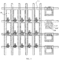
- FIG. 3 is a schematic plan view of another array substrate according to an embodiment of the present disclosure.
- the array substrate further includes second blocks 200 connected to the first blocks 110, and the second blocks 200 are located in a different layer from the first blocks 110.
- the second blocks 200 allow for further dispersion of the static charge in the gate lines 10.
- the second block 200 may be arranged such that its projection in a direction perpendicular to the array substrate covers the projection of the first block 110 in a direction perpendicular to the array substrate. I.e., the second block 200 has a size larger than the size of the first block 110. This allows for a further efficient dispersion of the electrostatic charge.
- the first block 110 and the second block 200 may be connected by a via or may be in direct contact.
- the number of the second blocks 200 included in the signal line leads is not limited.
- a further second block 200' is shown connected to the first block 100.
- the signal line lead may include more or fewer second blocks. In the case of a plurality of second blocks, they may be connected to each other by, for example, a via, although the present disclosure is not limited thereto.
- the second block bodies 200 and 200' and other conductive structures (e.g., pixel electrodes PE) in the array substrate can be manufactured by a one-time patterning process, thereby simplifying the process and reducing the manufacturing cost.
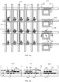
- FIG. 4a is a schematic plan view of another array substrate according to an embodiment of the present disclosure
- FIG. 4b is a combined illustration of cross-sectional views taken along line O-O', line A-A', and line BB' in FIG. 4a .
- An exemplary configuration of the first block 110 and the second block 200 will be further described below in conjunction with FIGS. 4a and 4b .
- FIG. 4a shows a plurality of gate lines L1 extending in the horizontal direction and a plurality of data lines 30 intersecting the gate lines L1.
- the gate lines L1 and the data lines 30 intersect to define a plurality of sub-pixels, and a plurality of thin film transistors TFT are disposed at respective ones of the intersections of the gate lines L1 and the data lines 30.
- FIG. 4b the cross-sectional view, taken along line O-O', shows the connection between the thin film transistor TFT and the pixel electrode PE in one of the sub-pixels.
- the thin film transistor is illustrated as a bottom gate type TFT in which a gate electrode G, a gate insulating layer GIL, an active layer AL, a source electrode S and a drain electrode D, and a passivation layer PL are sequentially formed on a base substrate BS.
- the thin film transistor may be a top gate type TFT.
- the first block 110 is in the same layer and of the same material as the gate line L1 (i.e., the gate electrode G in the thin film transistor)
- the second block 200 is in the same layer and of the same material as the data line 30 (i.e., the source electrode S and the drain electrode D in the thin film transistor)
- the further second block 200' is in the same layer and of the same material as the pixel electrode PE.
- the first block 110 and the gate lines may be formed by a one-time patterning process
- the second block 200 and the data lines may be formed by a one-time patterning process
- the second block 200' and the pixel electrodes PE may be formed by a one-time patterning process.
- the second block 200 and the second block 200' are connected by via(s)
- the first block 110 and the second block body 200' are connected by a via.
- the second block 200' includes the connecting portion 103 described above with respect to FIG. 2 , except that in the present embodiment the connecting portion 103 and the second block 200' are of an integral structure.
- the connecting portion 103 functions to disperse the static charge while functioning as a connection.
- the process can be simplified and the manufacturing cost reduced.
- the first block 110 may be in the same layer and of the same material as the gate lines, and the second block 200 may be in the same layer and of the same material as the data lines 30 (i.e., the source electrode and the drain electrode in the thin film transistor). That is, the first block and the gate lines are formed by a one-time patterning process, the second block and the data lines are formed by a one-time patterning process, and the first block 110 and the second block 200 may be connected by a via.
- the first block 110 may be in the same layer and of the same material as the gate lines, and the second block 200 may be in the same layer and of the same material as the pixel electrodes PE. That is, the first block and the gate lines are formed by a one-time patterning process, the second block 200 and the pixel electrodes PE are formed by a one-time patterning process, and the first block 110 and the second block 200 may be connected by a via.
- FIG. 5 is a schematic plan view of another array substrate according to an embodiment of the present disclosure.
- the array substrate further includes an electrostatic discharge line 40, and the signal line leads L2 are connected to the electrostatic discharge line 40 through electrostatic protection circuits 41.
- the electrostatic discharge line 40 When a certain amount of static charge is accumulated in the gate line leads, the accumulated static charge is delivered to the electrostatic discharge line 40 through the electrostatic protection circuits 41, and in turn, is discharged. In this way, the probability of the damage to the electronic devices in the display area caused by the electrostatic shock is reduced.
- FIG. 6 is an exemplary and schematic plan view of the electrostatic protection circuit of FIG. 5 .
- the electrostatic protection circuit 41 includes a first transistor T1 having a first gate electrode G1, a first source electrode S1, and a first drain electrode D1, and a second transistor T2 having a second gate electrode G2, a second source electrode S2, and a second drain electrode D2.
- the first transistor T1 and the second transistor T2 are juxtaposed along the extending direction of the electrostatic discharge line 40, and the first transistor T1 is closer to the gate line lead L2 than the second transistor T2.
- the first source S1 and the second drain D2 each have a U-shaped structure, both of which are integral with the electrostatic discharge line 40.
- the first drain electrode D1 and the second source electrode S2 are in the same layer and of the same material as the electrostatic discharge line 40.
- the first drain electrode D1 and the second source electrode S2 are of an integral structure, and this integral structure is connected to the gate line lead L2 through a first connection C1.
- the first gate electrode G1 and the second gate electrode G2 are in the same layer and of the same material as the gate line lead L2.
- the first gate electrode G1 and the gate line lead L2 are of an integral structure, and the second gate electrode G2 is connected to the electrostatic discharge line 40 through a second connection C2.
- first connection C1 and the second connection C2 described above may be disposed in the same layer as the pixel electrodes PE. That is, the first connection C1 and the second connection C2 are formed with the pixel electrodes PE by a one-time patterning process.
- FIG. 7 is a schematic plan view of another array substrate according to an embodiment of the present disclosure.
- the array substrate further includes common electrode lines 50 located in the display area 01, and a common electrode lead 51 located in the non-display area 02 and connected to the common electrode lines 50.
- the common electrode lead 51 includes a main lead 511 and sub-leads 512.
- the main lead 511 extends in the extending direction of the data lines 30, and the common electrode lines 50 and the sub-leads 512 extend in the extending direction of the gate lines L1.
- the common electrode lines 50 are connected to the main lead 511 through the sub-leads 512.
- the common electrode lines 50 and the sub-leads 512 may be of an integral structure, and the main lead 511 and the sub-leads 512 may be connected by connection portions.
- the main lead 511 of the common electrode lead 51 serves as the electrostatic discharge line 40 described above with respect to FIGS. 5 and 6 . Therefore, the main lead 511 and the gate line leads L2 are connected by respective electrostatic protection circuits 41. This is advantageous in reducing the wires in the array substrate, thereby reducing the complexity of the wiring.
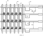
- FIG. 8 is a schematic plan view of another array substrate according to an embodiment of the present disclosure.
- the electrostatic discharge line 40 and the main lead 511 are two different wiring structures, as shown in FIG. 8 . This can prevent electrostatic discharge from affecting the common voltage on the common electrode.
- the electrostatic discharge line 40 may be disposed on the side of the main lead 511 near the display area 01 for ease of wiring.
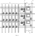
- FIG. 9 is a schematic plan view of another array substrate according to an embodiment of the present disclosure.
- the first blocks 110 are located between the main lead 511 and the electrostatic discharge line 40. This way, the main lead 511 and the electrostatic discharge line 40 shield the first blocks 110, thereby further reducing the adverse effect of the electrostatic charge in the first block 110 on the display area 01.
- the electrostatic discharge line 40 is connected to the main lead 511 through an additional electrostatic protection circuit 41.
- the electrostatic discharge line 40 may be connected to the main lead 511 through a wire. In this way, further dispersion of the electrostatic charge is facilitated.
- the gate lines (including the gate electrodes) and other conductive structures in the same layer as the gate lines may be made of one or more of chromium, tantalum, aluminum, titanium, magnesium, or copper, or alloys thereof.
- the data lines and other conductive structures in the same layer as the data lines may be made of one or more of chromium, tantalum, aluminum, titanium, magnesium or copper, or alloys thereof.
- the pixel electrodes and other conductive structures in the same layer as the pixel electrodes may be made of one or more of indium tin oxide (ITO), indium gallium zinc oxide (IGZO), or indium zinc oxide (IZO).
- the gate insulating layer may be made of one or more of silicon nitride, silicon oxide, or silicon oxynitride, and it may be either a single layer structure or a multilayer structure.
- the passivation layer may be made of one or more of silicon nitride, silicon oxide, or silicon oxynitride, or it may be a resin material.
- the passivation layer may be either a single layer structure or a multilayer structure.
- the active layer may be made of a polysilicon (a-Si) material. The present disclosure is not so limited.
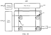
- FIG. 10 is a block diagram showing a display device 1000 according to an embodiment of the present disclosure.
- the display device 1000 includes a display panel 1100 for displaying an image, a gate driver 1200 for outputting gate scan signals to the display panel 1100, a data driver 1300 for outputting data voltages to the display panel 1100, and a timing controller 1400 for controlling the gate driver 1200 and the data driver 1300.
- the display panel 1100 includes an array substrate 1110 and a counter substrate 1120 opposite to the array substrate 1110.
- the display panel 110 further includes a liquid crystal layer (not shown) sandwiched between the array substrate 1110 and the counter substrate 1120, and the counter substrate 1120 may be a color filter substrate.
- the counter substrate 1120 may be a cover plate.
- the array substrate 1110 includes a plurality of pixel regions PX arranged in an array. The pixel regions PX are located at respective ones of the intersections of the plurality of gate lines GL and the plurality of data lines DL. Each of the pixel regions includes a pixel including a thin film transistor (not shown) and other associated components.
- the array substrate 1110 may take the form of any of the array substrates described above with respect to FIGS. 1 to 9 .
- the gate driver 1200 is electrically connected to first ends of the gate lines GL to sequentially apply gate scan signals to the respective gate lines GL.
- the gate driver 1200 may be directly mounted (e.g., integrated) in the array substrate 1110.
- the gate driver 1200 may be connected to the display panel 1100 through a Tape Carrier Package (TCP).
- TCP Tape Carrier Package
- the data driver 1300 is electrically connected to first ends of the data lines DL to output data voltages to the respective data lines DL.
- the data driver 1300 may include a plurality of data driving chips operating in parallel.
- the timing controller 1400 controls the operation of each of the gate driver 1200 and the data driver 1300. Specifically, the timing controller 1400 outputs data control signals and image data to control the driving operation of the data driver 1300, and outputs gate control signals to control the driving operation of the gate driver 1200. The data control signals and image data are applied to the data driver 1300. The gate control signals are applied to the gate driver 1200.
- the display device 1000 may be any product or component having a display function such as a liquid crystal panel, an electronic paper, an OLED panel, a mobile phone, a tablet computer, a television, a display, a notebook computer, a digital photo frame, a navigator, or the like.
- a display function such as a liquid crystal panel, an electronic paper, an OLED panel, a mobile phone, a tablet computer, a television, a display, a notebook computer, a digital photo frame, a navigator, or the like.
Landscapes
- Engineering & Computer Science (AREA)
- Physics & Mathematics (AREA)
- Theoretical Computer Science (AREA)
- General Physics & Mathematics (AREA)
- Power Engineering (AREA)
- Computer Hardware Design (AREA)
- General Engineering & Computer Science (AREA)
- Human Computer Interaction (AREA)
- Chemical & Material Sciences (AREA)
- Crystallography & Structural Chemistry (AREA)
- Nonlinear Science (AREA)
- Electromagnetism (AREA)
- Optics & Photonics (AREA)
- Mathematical Physics (AREA)
- Microelectronics & Electronic Packaging (AREA)
- Devices For Indicating Variable Information By Combining Individual Elements (AREA)
- Liquid Crystal (AREA)
Claims (15)
- Substrat de matrice, comprenant :une zone d'affichage (01) ;une zone de non-affichage (02) autre que la zone d'affichage (01) ;une pluralité de lignes de signaux (L1) dans la zone d'affichage (01) ; etune pluralité de conducteurs de lignes de signaux (L2) dans la zone de non-affichage (02) et connectés à des lignes respectives de la pluralité de lignes de signaux (L1),dans lequel chacun des conducteurs de lignes de signaux (L2) comprend un corps de conducteur (100) pourvu d'une borne de connexion (P) à l'extrémité du corps de conducteur qui est éloignée d'une ligne de signal respective (L1),dans lequel chacun des conducteurs de lignes de signaux (L2) comprend également un premier bloc (110) connecté à l'extrémité du corps de conducteur qui est adjacente à la ligne de signal respective (L1), dans lequel le premier bloc (110) est opposé à la borne de connexion (P) par rapport au corps de conducteur (100),caractérisé en ce que le premier bloc (110) a une surface supérieure ou égale à une surface d'un carré dont la longueur de côté est égale à 5 fois la largeur de la ligne de signal (L1).
- Substrat de matrice selon la revendication 1, dans lequel les lignes de signaux (L1) comprennent des lignes de grille, et dans lequel les conducteurs de lignes de signaux (L2) comprennent des conducteurs de lignes de grille.
- Substrat de matrice selon la revendication 2, dans lequel le premier bloc (110) a une taille dans une direction coupant une direction dans laquelle s'étendent les lignes de grille (L1), la taille étant inférieure à une distance entre deux lignes adjacentes des lignes de grille (L1) et supérieure ou égale à 1/3 de la distance entre les deux lignes adjacentes des lignes de grille (L1).
- Substrat de matrice selon la revendication 1, dans lequel au moins une partie du corps de conducteur (100) est solidaire du premier bloc (110).
- Substrat de matrice selon la revendication 4, dans lequel le corps de conducteur (100) s'étend dans une direction dans laquelle s'étend une ligne correspondante des lignes de signaux (L1),le corps de conducteur (100) comprend un premier corps de conducteur (101) solidaire de la ligne correspondante des lignes de signaux (L1) et du premier bloc (110), et un second corps de conducteur (102) séparé du premier corps de conducteur (101), etle substrat de matrice comprend en outre une pluralité de parties de connexion (103), chacune des parties de connexion (103) connectant les premier et second corps de conducteur (101, 102) d'un conducteur respectif de la pluralité de conducteurs de lignes de signaux (L2).
- Substrat de matrice selon la revendication 5, dans lequel chacun des conducteurs de lignes de signaux (L2) comprend en outre un second bloc (200) connecté au premier bloc (110) et se trouvant dans une couche différente du premier bloc (110), et dans lequel le second bloc (200) comprend une partie correspondante de la pluralité de parties de connexion (103).
- Substrat de matrice selon la revendication 1, dans lequel chacun des conducteurs de lignes de signaux (L2) comprend en outre un second bloc (200) connecté au premier bloc (110) et se trouvant dans une couche différente du premier bloc (110), et dans lequel chacun des conducteurs de lignes de signaux (L2) comprend de préférence une pluralité de seconds blocs (200, 200') connectés les uns aux autres.
- Substrat de matrice selon la revendication 7, dans lequel les lignes de signaux (L1) comprennent des lignes de grille (L1) et des lignes de données (30) coupant les lignes de grille,le premier bloc (110) se trouve dans la même couche et est réalisé en le même matériau que les lignes de grille (L1), et le second bloc (200) se trouve dans la même couche et est réalisé en le même matériau que les lignes de données (30), oudans lequelles lignes de signaux (L1) comprennent des lignes de grille (L1) et des lignes de données (30), les lignes de grille (L1) coupant les lignes de données (30) pour définir des électrodes de pixels (PE),le premier bloc (110) se trouve dans la même couche et est réalisé en le même matériau que les lignes de grille (L1), et le second bloc (200) se trouve dans la même couche et est réalisé en le même matériau que les électrodes pixels (PE), oudans lequelles lignes de signaux (L1) comprennent des lignes de grille (L1) et des lignes de données (30), les lignes de grille (L1) coupant les lignes de données (30) pour définir des électrodes de pixels (PE),le premier bloc (110) se trouve dans la même couche et est réalisé en le même matériau que les lignes de grille (L1), et chacun des conducteurs de lignes de signaux (L2) comprend deux des seconds blocs (200, 200'), l'un des deux seconds blocs (200) se trouvant dans la même couche et est réalisé en le même matériau que les lignes de données (30), et l'autre des deux seconds blocs (200') se trouvant dans la même couche et est réalisé en le même matériau que les électrodes pixels (PE).
- Substrat de matrice selon la revendication 7, dans lequel une projection du second bloc (200) dans une direction perpendiculaire au substrat de matrice recouvre une projection du premier bloc (110) dans une direction perpendiculaire au substrat de matrice.
- Substrat de matrice selon la revendication 1, comprenant en outre :une ligne de décharge électrostatique (40) dans la zone de non-affichage (02) et coupant les conducteurs de lignes de signaux (L2) ; etune pluralité de circuits de protection électrostatique (41) connectés entre des conducteurs respectifs des conducteurs de lignes de signaux (L2) et la ligne de décharge électrostatique (40) .
- Substrat de matrice selon la revendication 10, dans lequel les conducteurs de lignes de signaux (L2) comprennent des conducteurs de lignes de grille, et
chacun des circuits de protection électrostatique (41) comprend :un premier transistor (T1) comprenant une première électrode de grille (G1), une première électrode de source (S1) et une première électrode de drain (D1) ;un second transistor (T2) comprenant une seconde électrode de grille (G2), une seconde électrode de source (S2) et une seconde électrode de drain (D2),dans lequel le premier transistor (T1) et le second transistor (T2) sont juxtaposés le long d'une direction dans laquelle s'étend la ligne de décharge électrostatique (40), et le premier transistor (T1) est plus proche d'un conducteur correspondant des conducteurs de lignes de grille (L2) que le second transistor (T2),dans lequel la première électrode de source (S1) et la seconde électrode de drain (D2) sont des structures en forme de U et sont solidaires de la ligne de décharge électrostatique (40),dans lequel la première électrode de drain (D1) et la seconde électrode de source (S2) se trouvent dans la même couche et sont réalisées en le même matériau que la ligne de décharge électrostatique (40), et sont une structure intégrale connectée à un conducteur correspondant des conducteurs de lignes de grille (L2) par une première connexion (C1), etdans lequel la première électrode de grille (G1) et la seconde électrode de grille (G2) sont dans la même couche et réalisées en le même matériau que les conducteurs de lignes de grille (L2), la première électrode de grille (G1) étant solidaire du conducteur correspondant des conducteurs de lignes de grille (L2), et la seconde électrode de grille (G2) étant connectée à la ligne de décharge électrostatique (40) par une seconde connexion (C2). - Substrat de matrice selon la revendication 10, comprenant en outre :une pluralité de lignes d'électrodes communes (50) dans la zone d'affichage (01) ; etun conducteur d'électrode commun (51) dans la zone de non-affichage (02) et connecté aux lignes d'électrodes communes (50), le conducteur d'électrode commun (51) comprenant un conducteur principal (511) coupant les conducteurs de lignes de signaux (L2).
- Substrat de matrice selon la revendication 12, dans lequel le conducteur principal (511) est sélectionné dans un groupe consistant à servir de ligne de décharge électrostatique (40) et étant situé sur un côté de la ligne de décharge électrostatique (40) éloigné de la zone d'affichage (01), ou dans lequel le conducteur principal (511) se trouve sur un côté de la ligne de décharge électrostatique (40) éloigné de la zone d'affichage (01), et dans lequel le premier bloc (110) se trouve entre le conducteur principal (511) et la ligne de décharge électrostatique (40), ou
dans lequel le conducteur principal (511) se trouve sur un côté de la ligne de décharge électrostatique (40) éloigné de la zone d'affichage (01), et dans lequel le substrat de matrice comprend en outre un circuit de protection électrostatique supplémentaire (41) connecté entre la ligne de décharge électrostatique (40) et le conducteur principal (511). - Panneau d'affichage (1100) comprenant le substrat de matrice selon l'une quelconque des revendications 1 à 13.
- Dispositif d'affichage (1000) comprenant le panneau d'affichage (1100) selon la revendication 14.
Applications Claiming Priority (2)
| Application Number | Priority Date | Filing Date | Title |
|---|---|---|---|
| CN201721540228.5U CN207517281U (zh) | 2017-11-16 | 2017-11-16 | 一种阵列基板及显示装置 |
| PCT/CN2018/101261 WO2019095759A1 (fr) | 2017-11-16 | 2018-08-20 | Substrat de matrice, panneau d'affichage, et dispositif d'affichage |
Publications (3)
| Publication Number | Publication Date |
|---|---|
| EP3712874A1 EP3712874A1 (fr) | 2020-09-23 |
| EP3712874A4 EP3712874A4 (fr) | 2021-09-08 |
| EP3712874B1 true EP3712874B1 (fr) | 2022-12-14 |
Family
ID=62539624
Family Applications (1)
| Application Number | Title | Priority Date | Filing Date |
|---|---|---|---|
| EP18865350.5A Active EP3712874B1 (fr) | 2017-11-16 | 2018-08-20 | Substrat de matrice, panneau d'affichage, et dispositif d'affichage |
Country Status (4)
| Country | Link |
|---|---|
| US (1) | US10943543B2 (fr) |
| EP (1) | EP3712874B1 (fr) |
| CN (1) | CN207517281U (fr) |
| WO (1) | WO2019095759A1 (fr) |
Families Citing this family (11)
| Publication number | Priority date | Publication date | Assignee | Title |
|---|---|---|---|---|
| CN207517281U (zh) * | 2017-11-16 | 2018-06-19 | 京东方科技集团股份有限公司 | 一种阵列基板及显示装置 |
| CN207424484U (zh) * | 2017-11-27 | 2018-05-29 | 京东方科技集团股份有限公司 | 一种阵列基板及显示装置 |
| TWI667780B (zh) * | 2018-08-02 | 2019-08-01 | 友達光電股份有限公司 | 顯示面板 |
| CN116417471A (zh) | 2020-03-30 | 2023-07-11 | 厦门天马微电子有限公司 | 一种阵列基板、显示面板及显示装置 |
| CN112259593B (zh) * | 2020-10-22 | 2023-05-30 | 武汉华星光电技术有限公司 | 阵列基板、阵列基板的制作方法和显示装置 |
| CN113540129B (zh) * | 2021-07-20 | 2023-09-22 | 合肥鑫晟光电科技有限公司 | 显示面板及其制备方法、显示装置 |
| CN117480446A (zh) * | 2022-05-25 | 2024-01-30 | 京东方科技集团股份有限公司 | 阵列基板以及显示装置 |
| US20240429244A1 (en) * | 2023-01-03 | 2024-12-26 | Chengdu Boe Display Sci-Tech Co., Ltd. | Array substrate, display panel and display device |
| CN120188097A (zh) * | 2023-09-28 | 2025-06-20 | 京东方科技集团股份有限公司 | 显示基板 |
| CN118471984B (zh) * | 2024-05-10 | 2025-10-10 | 惠科股份有限公司 | 阵列基板及显示面板 |
| CN118507491B (zh) * | 2024-05-10 | 2025-09-16 | 惠科股份有限公司 | 阵列基板及显示面板 |
Family Cites Families (22)
| Publication number | Priority date | Publication date | Assignee | Title |
|---|---|---|---|---|
| JP3290772B2 (ja) * | 1993-08-18 | 2002-06-10 | 株式会社東芝 | 表示装置 |
| JP3072707B2 (ja) * | 1995-10-31 | 2000-08-07 | インターナショナル・ビジネス・マシーンズ・コーポレ−ション | 液晶表示装置及びその製造方法 |
| KR100242437B1 (ko) * | 1996-08-07 | 2000-02-01 | 윤종용 | 액정 모듈 및 그 제조 방법 |
| JP2004247533A (ja) | 2003-02-14 | 2004-09-02 | Casio Comput Co Ltd | アクティブマトリックスパネル |
| KR100847640B1 (ko) | 2006-05-23 | 2008-07-21 | 가시오게산키 가부시키가이샤 | 표시장치 |
| JP2007316104A (ja) | 2006-05-23 | 2007-12-06 | Casio Comput Co Ltd | 表示装置 |
| CN100533734C (zh) * | 2006-12-11 | 2009-08-26 | 中华映管股份有限公司 | 主动元件阵列基板 |
| CN101114069A (zh) * | 2007-06-26 | 2008-01-30 | 河北冀雅电子有限公司 | 一种液晶显示器件光刻版图的防静电方法 |
| KR101420444B1 (ko) * | 2008-12-24 | 2014-08-13 | 엘지디스플레이 주식회사 | 액정표시장치 |
| TW201033707A (en) * | 2009-03-04 | 2010-09-16 | Au Optronics Corp | Flat display panel |
| KR101791577B1 (ko) * | 2011-01-17 | 2017-10-31 | 삼성디스플레이 주식회사 | 박막 트랜지스터 표시판 |
| CN102654699A (zh) * | 2011-09-29 | 2012-09-05 | 北京京东方光电科技有限公司 | 一种阵列基板及线缺陷维修方法 |
| CN104035217B (zh) | 2014-05-21 | 2016-08-24 | 深圳市华星光电技术有限公司 | 显示器阵列基板的外围测试线路以及液晶显示面板 |
| JP2016057344A (ja) * | 2014-09-05 | 2016-04-21 | 株式会社ジャパンディスプレイ | 表示装置 |
| CN104615322A (zh) * | 2015-02-03 | 2015-05-13 | 上海天马微电子有限公司 | 触控结构、基板、阵列基板及显示装置 |
| US10067585B2 (en) * | 2015-12-28 | 2018-09-04 | Lg Display Co., Ltd. | Display device with multilayered capacitor |
| KR102457244B1 (ko) * | 2016-05-19 | 2022-10-21 | 삼성디스플레이 주식회사 | 표시 장치 |
| CN106200172B (zh) * | 2016-07-14 | 2020-06-02 | 京东方科技集团股份有限公司 | 一种阵列基板及显示装置 |
| KR102597681B1 (ko) * | 2016-09-19 | 2023-11-06 | 삼성디스플레이 주식회사 | 표시 장치 |
| KR102432386B1 (ko) * | 2017-07-12 | 2022-08-12 | 삼성디스플레이 주식회사 | 표시 장치 |
| KR102341124B1 (ko) * | 2017-09-26 | 2021-12-22 | 삼성디스플레이 주식회사 | 전자패널, 표시장치, 및 그 제조 방법 |
| CN207517281U (zh) * | 2017-11-16 | 2018-06-19 | 京东方科技集团股份有限公司 | 一种阵列基板及显示装置 |
-
2017
- 2017-11-16 CN CN201721540228.5U patent/CN207517281U/zh active Active
-
2018
- 2018-08-20 EP EP18865350.5A patent/EP3712874B1/fr active Active
- 2018-08-20 WO PCT/CN2018/101261 patent/WO2019095759A1/fr not_active Ceased
- 2018-08-20 US US16/336,381 patent/US10943543B2/en active Active
Also Published As
| Publication number | Publication date |
|---|---|
| US20200357343A1 (en) | 2020-11-12 |
| WO2019095759A1 (fr) | 2019-05-23 |
| EP3712874A4 (fr) | 2021-09-08 |
| CN207517281U (zh) | 2018-06-19 |
| EP3712874A1 (fr) | 2020-09-23 |
| US10943543B2 (en) | 2021-03-09 |
Similar Documents
| Publication | Publication Date | Title |
|---|---|---|
| EP3712874B1 (fr) | Substrat de matrice, panneau d'affichage, et dispositif d'affichage | |
| EP3712692B1 (fr) | Substrat de réseau, panneau d'affichage et dispositif d'affichage | |
| US9798203B2 (en) | Semiconductor device and display device | |
| US20210223897A1 (en) | Display device with sensor | |
| US9443781B2 (en) | Display device | |
| US9632378B2 (en) | Display device | |
| US9263387B2 (en) | GOA circuit of array substrate and display apparatus | |
| US8908114B2 (en) | Liquid crystal display device | |
| US9529236B2 (en) | Pixel structure and display panel | |
| US9244317B2 (en) | Active matrix substrate and display device | |
| EP2477064A1 (fr) | Dispositif d'affichage à cristaux liquides et procédé de fabrication de celui-ci | |
| KR102396466B1 (ko) | 유기 발광 표시 장치 | |
| US9443885B2 (en) | Semiconductor device and display device | |
| US9164334B2 (en) | Display device and method of manufacturing same | |
| US20190280013A1 (en) | Active matrix substrate and display panel | |
| US10067393B2 (en) | Thin film display panel and liquid crystal display device including the same | |
| US20150279865A1 (en) | Semiconductor device and display device | |
| KR101494205B1 (ko) | 표시기판, 이의 제조방법 및 이를 갖는 표시장치 | |
| US20200159077A1 (en) | Array substrate, array substrate body component, and display device | |
| KR102410396B1 (ko) | 수평 전계형 액정 표시장치 및 그 제조방법 | |
| US12066729B2 (en) | Display panel and display device | |
| US20260111087A1 (en) | Active matrix substrate, display panel, and display device | |
| US20250351576A1 (en) | Display device and method of producing display device |
Legal Events
| Date | Code | Title | Description |
|---|---|---|---|
| STAA | Information on the status of an ep patent application or granted ep patent |
Free format text: STATUS: UNKNOWN |
|
| STAA | Information on the status of an ep patent application or granted ep patent |
Free format text: STATUS: THE INTERNATIONAL PUBLICATION HAS BEEN MADE |
|
| PUAI | Public reference made under article 153(3) epc to a published international application that has entered the european phase |
Free format text: ORIGINAL CODE: 0009012 |
|
| STAA | Information on the status of an ep patent application or granted ep patent |
Free format text: STATUS: REQUEST FOR EXAMINATION WAS MADE |
|
| 17P | Request for examination filed |
Effective date: 20200203 |
|
| AK | Designated contracting states |
Kind code of ref document: A1 Designated state(s): AL AT BE BG CH CY CZ DE DK EE ES FI FR GB GR HR HU IE IS IT LI LT LU LV MC MK MT NL NO PL PT RO RS SE SI SK SM TR |
|
| AX | Request for extension of the european patent |
Extension state: BA ME |
|
| DAV | Request for validation of the european patent (deleted) | ||
| DAX | Request for extension of the european patent (deleted) | ||
| A4 | Supplementary search report drawn up and despatched |
Effective date: 20210810 |
|
| RIC1 | Information provided on ipc code assigned before grant |
Ipc: G02F 1/1362 20060101ALI20210804BHEP Ipc: G02F 1/1345 20060101ALI20210804BHEP Ipc: G09F 9/00 20060101AFI20210804BHEP |
|
| GRAP | Despatch of communication of intention to grant a patent |
Free format text: ORIGINAL CODE: EPIDOSNIGR1 |
|
| STAA | Information on the status of an ep patent application or granted ep patent |
Free format text: STATUS: GRANT OF PATENT IS INTENDED |
|
| INTG | Intention to grant announced |
Effective date: 20220704 |
|
| GRAS | Grant fee paid |
Free format text: ORIGINAL CODE: EPIDOSNIGR3 |
|
| GRAA | (expected) grant |
Free format text: ORIGINAL CODE: 0009210 |
|
| STAA | Information on the status of an ep patent application or granted ep patent |
Free format text: STATUS: THE PATENT HAS BEEN GRANTED |
|
| AK | Designated contracting states |
Kind code of ref document: B1 Designated state(s): AL AT BE BG CH CY CZ DE DK EE ES FI FR GB GR HR HU IE IS IT LI LT LU LV MC MK MT NL NO PL PT RO RS SE SI SK SM TR |
|
| REG | Reference to a national code |
Ref country code: GB Ref legal event code: FG4D |
|
| REG | Reference to a national code |
Ref country code: CH Ref legal event code: EP |
|
| REG | Reference to a national code |
Ref country code: DE Ref legal event code: R096 Ref document number: 602018044358 Country of ref document: DE |
|
| REG | Reference to a national code |
Ref country code: IE Ref legal event code: FG4D |
|
| REG | Reference to a national code |
Ref country code: AT Ref legal event code: REF Ref document number: 1538157 Country of ref document: AT Kind code of ref document: T Effective date: 20230115 |
|
| REG | Reference to a national code |
Ref country code: LT Ref legal event code: MG9D |
|
| REG | Reference to a national code |
Ref country code: NL Ref legal event code: MP Effective date: 20221214 |
|
| PG25 | Lapsed in a contracting state [announced via postgrant information from national office to epo] |
Ref country code: SE Free format text: LAPSE BECAUSE OF FAILURE TO SUBMIT A TRANSLATION OF THE DESCRIPTION OR TO PAY THE FEE WITHIN THE PRESCRIBED TIME-LIMIT Effective date: 20221214 Ref country code: NO Free format text: LAPSE BECAUSE OF FAILURE TO SUBMIT A TRANSLATION OF THE DESCRIPTION OR TO PAY THE FEE WITHIN THE PRESCRIBED TIME-LIMIT Effective date: 20230314 Ref country code: LT Free format text: LAPSE BECAUSE OF FAILURE TO SUBMIT A TRANSLATION OF THE DESCRIPTION OR TO PAY THE FEE WITHIN THE PRESCRIBED TIME-LIMIT Effective date: 20221214 Ref country code: FI Free format text: LAPSE BECAUSE OF FAILURE TO SUBMIT A TRANSLATION OF THE DESCRIPTION OR TO PAY THE FEE WITHIN THE PRESCRIBED TIME-LIMIT Effective date: 20221214 |
|
| REG | Reference to a national code |
Ref country code: AT Ref legal event code: MK05 Ref document number: 1538157 Country of ref document: AT Kind code of ref document: T Effective date: 20221214 |
|
| PG25 | Lapsed in a contracting state [announced via postgrant information from national office to epo] |
Ref country code: RS Free format text: LAPSE BECAUSE OF FAILURE TO SUBMIT A TRANSLATION OF THE DESCRIPTION OR TO PAY THE FEE WITHIN THE PRESCRIBED TIME-LIMIT Effective date: 20221214 Ref country code: LV Free format text: LAPSE BECAUSE OF FAILURE TO SUBMIT A TRANSLATION OF THE DESCRIPTION OR TO PAY THE FEE WITHIN THE PRESCRIBED TIME-LIMIT Effective date: 20221214 Ref country code: HR Free format text: LAPSE BECAUSE OF FAILURE TO SUBMIT A TRANSLATION OF THE DESCRIPTION OR TO PAY THE FEE WITHIN THE PRESCRIBED TIME-LIMIT Effective date: 20221214 Ref country code: GR Free format text: LAPSE BECAUSE OF FAILURE TO SUBMIT A TRANSLATION OF THE DESCRIPTION OR TO PAY THE FEE WITHIN THE PRESCRIBED TIME-LIMIT Effective date: 20230315 |
|
| PG25 | Lapsed in a contracting state [announced via postgrant information from national office to epo] |
Ref country code: NL Free format text: LAPSE BECAUSE OF FAILURE TO SUBMIT A TRANSLATION OF THE DESCRIPTION OR TO PAY THE FEE WITHIN THE PRESCRIBED TIME-LIMIT Effective date: 20221214 |
|
| PG25 | Lapsed in a contracting state [announced via postgrant information from national office to epo] |
Ref country code: SM Free format text: LAPSE BECAUSE OF FAILURE TO SUBMIT A TRANSLATION OF THE DESCRIPTION OR TO PAY THE FEE WITHIN THE PRESCRIBED TIME-LIMIT Effective date: 20221214 Ref country code: RO Free format text: LAPSE BECAUSE OF FAILURE TO SUBMIT A TRANSLATION OF THE DESCRIPTION OR TO PAY THE FEE WITHIN THE PRESCRIBED TIME-LIMIT Effective date: 20221214 Ref country code: PT Free format text: LAPSE BECAUSE OF FAILURE TO SUBMIT A TRANSLATION OF THE DESCRIPTION OR TO PAY THE FEE WITHIN THE PRESCRIBED TIME-LIMIT Effective date: 20230414 Ref country code: ES Free format text: LAPSE BECAUSE OF FAILURE TO SUBMIT A TRANSLATION OF THE DESCRIPTION OR TO PAY THE FEE WITHIN THE PRESCRIBED TIME-LIMIT Effective date: 20221214 Ref country code: EE Free format text: LAPSE BECAUSE OF FAILURE TO SUBMIT A TRANSLATION OF THE DESCRIPTION OR TO PAY THE FEE WITHIN THE PRESCRIBED TIME-LIMIT Effective date: 20221214 Ref country code: CZ Free format text: LAPSE BECAUSE OF FAILURE TO SUBMIT A TRANSLATION OF THE DESCRIPTION OR TO PAY THE FEE WITHIN THE PRESCRIBED TIME-LIMIT Effective date: 20221214 Ref country code: AT Free format text: LAPSE BECAUSE OF FAILURE TO SUBMIT A TRANSLATION OF THE DESCRIPTION OR TO PAY THE FEE WITHIN THE PRESCRIBED TIME-LIMIT Effective date: 20221214 |
|
| PG25 | Lapsed in a contracting state [announced via postgrant information from national office to epo] |
Ref country code: SK Free format text: LAPSE BECAUSE OF FAILURE TO SUBMIT A TRANSLATION OF THE DESCRIPTION OR TO PAY THE FEE WITHIN THE PRESCRIBED TIME-LIMIT Effective date: 20221214 Ref country code: PL Free format text: LAPSE BECAUSE OF FAILURE TO SUBMIT A TRANSLATION OF THE DESCRIPTION OR TO PAY THE FEE WITHIN THE PRESCRIBED TIME-LIMIT Effective date: 20221214 Ref country code: IS Free format text: LAPSE BECAUSE OF FAILURE TO SUBMIT A TRANSLATION OF THE DESCRIPTION OR TO PAY THE FEE WITHIN THE PRESCRIBED TIME-LIMIT Effective date: 20230414 Ref country code: AL Free format text: LAPSE BECAUSE OF FAILURE TO SUBMIT A TRANSLATION OF THE DESCRIPTION OR TO PAY THE FEE WITHIN THE PRESCRIBED TIME-LIMIT Effective date: 20221214 |
|
| REG | Reference to a national code |
Ref country code: DE Ref legal event code: R097 Ref document number: 602018044358 Country of ref document: DE |
|
| PLBE | No opposition filed within time limit |
Free format text: ORIGINAL CODE: 0009261 |
|
| STAA | Information on the status of an ep patent application or granted ep patent |
Free format text: STATUS: NO OPPOSITION FILED WITHIN TIME LIMIT |
|
| PG25 | Lapsed in a contracting state [announced via postgrant information from national office to epo] |
Ref country code: DK Free format text: LAPSE BECAUSE OF FAILURE TO SUBMIT A TRANSLATION OF THE DESCRIPTION OR TO PAY THE FEE WITHIN THE PRESCRIBED TIME-LIMIT Effective date: 20221214 |
|
| 26N | No opposition filed |
Effective date: 20230915 |
|
| PG25 | Lapsed in a contracting state [announced via postgrant information from national office to epo] |
Ref country code: SI Free format text: LAPSE BECAUSE OF FAILURE TO SUBMIT A TRANSLATION OF THE DESCRIPTION OR TO PAY THE FEE WITHIN THE PRESCRIBED TIME-LIMIT Effective date: 20221214 |
|
| PG25 | Lapsed in a contracting state [announced via postgrant information from national office to epo] |
Ref country code: MC Free format text: LAPSE BECAUSE OF FAILURE TO SUBMIT A TRANSLATION OF THE DESCRIPTION OR TO PAY THE FEE WITHIN THE PRESCRIBED TIME-LIMIT Effective date: 20221214 |
|
| REG | Reference to a national code |
Ref country code: CH Ref legal event code: PL |
|
| PG25 | Lapsed in a contracting state [announced via postgrant information from national office to epo] |
Ref country code: MC Free format text: LAPSE BECAUSE OF FAILURE TO SUBMIT A TRANSLATION OF THE DESCRIPTION OR TO PAY THE FEE WITHIN THE PRESCRIBED TIME-LIMIT Effective date: 20221214 |
|
| PG25 | Lapsed in a contracting state [announced via postgrant information from national office to epo] |
Ref country code: LU Free format text: LAPSE BECAUSE OF NON-PAYMENT OF DUE FEES Effective date: 20230820 |
|
| GBPC | Gb: european patent ceased through non-payment of renewal fee |
Effective date: 20230820 |
|
| PG25 | Lapsed in a contracting state [announced via postgrant information from national office to epo] |
Ref country code: LU Free format text: LAPSE BECAUSE OF NON-PAYMENT OF DUE FEES Effective date: 20230820 Ref country code: CH Free format text: LAPSE BECAUSE OF NON-PAYMENT OF DUE FEES Effective date: 20230831 |
|
| REG | Reference to a national code |
Ref country code: BE Ref legal event code: MM Effective date: 20230831 |
|
| REG | Reference to a national code |
Ref country code: IE Ref legal event code: MM4A |
|
| PG25 | Lapsed in a contracting state [announced via postgrant information from national office to epo] |
Ref country code: IT Free format text: LAPSE BECAUSE OF FAILURE TO SUBMIT A TRANSLATION OF THE DESCRIPTION OR TO PAY THE FEE WITHIN THE PRESCRIBED TIME-LIMIT Effective date: 20221214 |
|
| PG25 | Lapsed in a contracting state [announced via postgrant information from national office to epo] |
Ref country code: IE Free format text: LAPSE BECAUSE OF NON-PAYMENT OF DUE FEES Effective date: 20230820 |
|
| PG25 | Lapsed in a contracting state [announced via postgrant information from national office to epo] |
Ref country code: GB Free format text: LAPSE BECAUSE OF NON-PAYMENT OF DUE FEES Effective date: 20230820 |
|
| PG25 | Lapsed in a contracting state [announced via postgrant information from national office to epo] |
Ref country code: IE Free format text: LAPSE BECAUSE OF NON-PAYMENT OF DUE FEES Effective date: 20230820 Ref country code: GB Free format text: LAPSE BECAUSE OF NON-PAYMENT OF DUE FEES Effective date: 20230820 Ref country code: FR Free format text: LAPSE BECAUSE OF NON-PAYMENT OF DUE FEES Effective date: 20230831 |
|
| PG25 | Lapsed in a contracting state [announced via postgrant information from national office to epo] |
Ref country code: BE Free format text: LAPSE BECAUSE OF NON-PAYMENT OF DUE FEES Effective date: 20230831 |
|
| PG25 | Lapsed in a contracting state [announced via postgrant information from national office to epo] |
Ref country code: BG Free format text: LAPSE BECAUSE OF FAILURE TO SUBMIT A TRANSLATION OF THE DESCRIPTION OR TO PAY THE FEE WITHIN THE PRESCRIBED TIME-LIMIT Effective date: 20221214 |
|
| PG25 | Lapsed in a contracting state [announced via postgrant information from national office to epo] |
Ref country code: BG Free format text: LAPSE BECAUSE OF FAILURE TO SUBMIT A TRANSLATION OF THE DESCRIPTION OR TO PAY THE FEE WITHIN THE PRESCRIBED TIME-LIMIT Effective date: 20221214 |
|
| PG25 | Lapsed in a contracting state [announced via postgrant information from national office to epo] |
Ref country code: CY Free format text: LAPSE BECAUSE OF FAILURE TO SUBMIT A TRANSLATION OF THE DESCRIPTION OR TO PAY THE FEE WITHIN THE PRESCRIBED TIME-LIMIT; INVALID AB INITIO Effective date: 20180820 |
|
| PG25 | Lapsed in a contracting state [announced via postgrant information from national office to epo] |
Ref country code: HU Free format text: LAPSE BECAUSE OF FAILURE TO SUBMIT A TRANSLATION OF THE DESCRIPTION OR TO PAY THE FEE WITHIN THE PRESCRIBED TIME-LIMIT; INVALID AB INITIO Effective date: 20180820 |
|
| PGFP | Annual fee paid to national office [announced via postgrant information from national office to epo] |
Ref country code: DE Payment date: 20250820 Year of fee payment: 8 |
|
| PG25 | Lapsed in a contracting state [announced via postgrant information from national office to epo] |
Ref country code: TR Free format text: LAPSE BECAUSE OF FAILURE TO SUBMIT A TRANSLATION OF THE DESCRIPTION OR TO PAY THE FEE WITHIN THE PRESCRIBED TIME-LIMIT Effective date: 20221214 |