EP3712982A1 - Elektronische vorrichtung - Google Patents
Elektronische vorrichtung Download PDFInfo
- Publication number
- EP3712982A1 EP3712982A1 EP20163904.4A EP20163904A EP3712982A1 EP 3712982 A1 EP3712982 A1 EP 3712982A1 EP 20163904 A EP20163904 A EP 20163904A EP 3712982 A1 EP3712982 A1 EP 3712982A1
- Authority
- EP
- European Patent Office
- Prior art keywords
- cell
- electronic device
- board
- circuit board
- protection unit
- Prior art date
- Legal status (The legal status is an assumption and is not a legal conclusion. Google has not performed a legal analysis and makes no representation as to the accuracy of the status listed.)
- Pending
Links
Images


Classifications
-
- H—ELECTRICITY
- H01—ELECTRIC ELEMENTS
- H01M—PROCESSES OR MEANS, e.g. BATTERIES, FOR THE DIRECT CONVERSION OF CHEMICAL ENERGY INTO ELECTRICAL ENERGY
- H01M10/00—Secondary cells; Manufacture thereof
- H01M10/42—Methods or arrangements for servicing or maintenance of secondary cells or secondary half-cells
- H01M10/425—Structural combination with electronic components, e.g. electronic circuits integrated to the outside of the casing
-
- H—ELECTRICITY
- H01—ELECTRIC ELEMENTS
- H01M—PROCESSES OR MEANS, e.g. BATTERIES, FOR THE DIRECT CONVERSION OF CHEMICAL ENERGY INTO ELECTRICAL ENERGY
- H01M10/00—Secondary cells; Manufacture thereof
- H01M10/05—Accumulators with non-aqueous electrolyte
- H01M10/052—Li-accumulators
- H01M10/0525—Rocking-chair batteries, i.e. batteries with lithium insertion or intercalation in both electrodes; Lithium-ion batteries
-
- H—ELECTRICITY
- H01—ELECTRIC ELEMENTS
- H01M—PROCESSES OR MEANS, e.g. BATTERIES, FOR THE DIRECT CONVERSION OF CHEMICAL ENERGY INTO ELECTRICAL ENERGY
- H01M10/00—Secondary cells; Manufacture thereof
- H01M10/05—Accumulators with non-aqueous electrolyte
- H01M10/058—Construction or manufacture
-
- H—ELECTRICITY
- H01—ELECTRIC ELEMENTS
- H01M—PROCESSES OR MEANS, e.g. BATTERIES, FOR THE DIRECT CONVERSION OF CHEMICAL ENERGY INTO ELECTRICAL ENERGY
- H01M10/00—Secondary cells; Manufacture thereof
- H01M10/60—Heating or cooling; Temperature control
- H01M10/61—Types of temperature control
- H01M10/613—Cooling or keeping cold
-
- H—ELECTRICITY
- H01—ELECTRIC ELEMENTS
- H01M—PROCESSES OR MEANS, e.g. BATTERIES, FOR THE DIRECT CONVERSION OF CHEMICAL ENERGY INTO ELECTRICAL ENERGY
- H01M50/00—Constructional details or processes of manufacture of the non-active parts of electrochemical cells other than fuel cells, e.g. hybrid cells
- H01M50/50—Current conducting connections for cells or batteries
- H01M50/531—Electrode connections inside a battery casing
-
- H—ELECTRICITY
- H01—ELECTRIC ELEMENTS
- H01M—PROCESSES OR MEANS, e.g. BATTERIES, FOR THE DIRECT CONVERSION OF CHEMICAL ENERGY INTO ELECTRICAL ENERGY
- H01M50/00—Constructional details or processes of manufacture of the non-active parts of electrochemical cells other than fuel cells, e.g. hybrid cells
- H01M50/50—Current conducting connections for cells or batteries
- H01M50/543—Terminals
-
- H—ELECTRICITY
- H01—ELECTRIC ELEMENTS
- H01M—PROCESSES OR MEANS, e.g. BATTERIES, FOR THE DIRECT CONVERSION OF CHEMICAL ENERGY INTO ELECTRICAL ENERGY
- H01M50/00—Constructional details or processes of manufacture of the non-active parts of electrochemical cells other than fuel cells, e.g. hybrid cells
- H01M50/50—Current conducting connections for cells or batteries
- H01M50/543—Terminals
- H01M50/564—Terminals characterised by their manufacturing process
- H01M50/566—Terminals characterised by their manufacturing process by welding, soldering or brazing
-
- H—ELECTRICITY
- H01—ELECTRIC ELEMENTS
- H01M—PROCESSES OR MEANS, e.g. BATTERIES, FOR THE DIRECT CONVERSION OF CHEMICAL ENERGY INTO ELECTRICAL ENERGY
- H01M50/00—Constructional details or processes of manufacture of the non-active parts of electrochemical cells other than fuel cells, e.g. hybrid cells
- H01M50/50—Current conducting connections for cells or batteries
- H01M50/543—Terminals
- H01M50/564—Terminals characterised by their manufacturing process
- H01M50/567—Terminals characterised by their manufacturing process by fixing means, e.g. screws, rivets or bolts
-
- H—ELECTRICITY
- H01—ELECTRIC ELEMENTS
- H01M—PROCESSES OR MEANS, e.g. BATTERIES, FOR THE DIRECT CONVERSION OF CHEMICAL ENERGY INTO ELECTRICAL ENERGY
- H01M10/00—Secondary cells; Manufacture thereof
- H01M10/42—Methods or arrangements for servicing or maintenance of secondary cells or secondary half-cells
- H01M10/425—Structural combination with electronic components, e.g. electronic circuits integrated to the outside of the casing
- H01M2010/4271—Battery management systems including electronic circuits, e.g. control of current or voltage to keep battery in healthy state, cell balancing
-
- H—ELECTRICITY
- H01—ELECTRIC ELEMENTS
- H01M—PROCESSES OR MEANS, e.g. BATTERIES, FOR THE DIRECT CONVERSION OF CHEMICAL ENERGY INTO ELECTRICAL ENERGY
- H01M2200/00—Safety devices for primary or secondary batteries
-
- H—ELECTRICITY
- H01—ELECTRIC ELEMENTS
- H01M—PROCESSES OR MEANS, e.g. BATTERIES, FOR THE DIRECT CONVERSION OF CHEMICAL ENERGY INTO ELECTRICAL ENERGY
- H01M2200/00—Safety devices for primary or secondary batteries
- H01M2200/10—Temperature sensitive devices
-
- H—ELECTRICITY
- H01—ELECTRIC ELEMENTS
- H01M—PROCESSES OR MEANS, e.g. BATTERIES, FOR THE DIRECT CONVERSION OF CHEMICAL ENERGY INTO ELECTRICAL ENERGY
- H01M2200/00—Safety devices for primary or secondary batteries
- H01M2200/20—Pressure-sensitive devices
-
- H—ELECTRICITY
- H01—ELECTRIC ELEMENTS
- H01M—PROCESSES OR MEANS, e.g. BATTERIES, FOR THE DIRECT CONVERSION OF CHEMICAL ENERGY INTO ELECTRICAL ENERGY
- H01M2220/00—Batteries for particular applications
- H01M2220/30—Batteries in portable systems, e.g. mobile phone, laptop
-
- H—ELECTRICITY
- H01—ELECTRIC ELEMENTS
- H01M—PROCESSES OR MEANS, e.g. BATTERIES, FOR THE DIRECT CONVERSION OF CHEMICAL ENERGY INTO ELECTRICAL ENERGY
- H01M50/00—Constructional details or processes of manufacture of the non-active parts of electrochemical cells other than fuel cells, e.g. hybrid cells
- H01M50/20—Mountings; Secondary casings or frames; Racks, modules or packs; Suspension devices; Shock absorbers; Transport or carrying devices; Holders
- H01M50/204—Racks, modules or packs for multiple batteries or multiple cells
- H01M50/207—Racks, modules or packs for multiple batteries or multiple cells characterised by their shape
- H01M50/209—Racks, modules or packs for multiple batteries or multiple cells characterised by their shape adapted for prismatic or rectangular cells
-
- H—ELECTRICITY
- H01—ELECTRIC ELEMENTS
- H01M—PROCESSES OR MEANS, e.g. BATTERIES, FOR THE DIRECT CONVERSION OF CHEMICAL ENERGY INTO ELECTRICAL ENERGY
- H01M50/00—Constructional details or processes of manufacture of the non-active parts of electrochemical cells other than fuel cells, e.g. hybrid cells
- H01M50/50—Current conducting connections for cells or batteries
- H01M50/543—Terminals
- H01M50/547—Terminals characterised by the disposition of the terminals on the cells
- H01M50/55—Terminals characterised by the disposition of the terminals on the cells on the same side of the cell
-
- H—ELECTRICITY
- H01—ELECTRIC ELEMENTS
- H01M—PROCESSES OR MEANS, e.g. BATTERIES, FOR THE DIRECT CONVERSION OF CHEMICAL ENERGY INTO ELECTRICAL ENERGY
- H01M50/00—Constructional details or processes of manufacture of the non-active parts of electrochemical cells other than fuel cells, e.g. hybrid cells
- H01M50/50—Current conducting connections for cells or batteries
- H01M50/543—Terminals
- H01M50/552—Terminals characterised by their shape
- H01M50/553—Terminals adapted for prismatic, pouch or rectangular cells
-
- Y—GENERAL TAGGING OF NEW TECHNOLOGICAL DEVELOPMENTS; GENERAL TAGGING OF CROSS-SECTIONAL TECHNOLOGIES SPANNING OVER SEVERAL SECTIONS OF THE IPC; TECHNICAL SUBJECTS COVERED BY FORMER USPC CROSS-REFERENCE ART COLLECTIONS [XRACs] AND DIGESTS
- Y02—TECHNOLOGIES OR APPLICATIONS FOR MITIGATION OR ADAPTATION AGAINST CLIMATE CHANGE
- Y02E—REDUCTION OF GREENHOUSE GAS [GHG] EMISSIONS, RELATED TO ENERGY GENERATION, TRANSMISSION OR DISTRIBUTION
- Y02E60/00—Enabling technologies; Technologies with a potential or indirect contribution to GHG emissions mitigation
- Y02E60/10—Energy storage using batteries
-
- Y—GENERAL TAGGING OF NEW TECHNOLOGICAL DEVELOPMENTS; GENERAL TAGGING OF CROSS-SECTIONAL TECHNOLOGIES SPANNING OVER SEVERAL SECTIONS OF THE IPC; TECHNICAL SUBJECTS COVERED BY FORMER USPC CROSS-REFERENCE ART COLLECTIONS [XRACs] AND DIGESTS
- Y02—TECHNOLOGIES OR APPLICATIONS FOR MITIGATION OR ADAPTATION AGAINST CLIMATE CHANGE
- Y02P—CLIMATE CHANGE MITIGATION TECHNOLOGIES IN THE PRODUCTION OR PROCESSING OF GOODS
- Y02P70/00—Climate change mitigation technologies in the production process for final industrial or consumer products
- Y02P70/50—Manufacturing or production processes characterised by the final manufactured product
Definitions
- the present disclosure relates to a technical field of communication devices, and more particularly, to an electronic device.
- Lithium-ion batteries have advantages of high energy density and high reliability, and are widely used in mobile terminals, smart mobile homes, smart aircrafts and other applications. Developing high-capacity lithium batteries has been an area of interest in recent years and will trend in the future, and this trend may also be a new challenge for cell assemblers.
- most assembly schemes of batteries and electronic terminals include first coupling a cell to a cell protection unit, then encapsulating, and finally transporting the encapsulated battery to a terminal processing factory to be assembled with a main board in a host casing.
- the above technical schemes have the following defects.
- the battery encapsulation results in a risk of damaging the cell and causes a safety hazard.
- the encapsulation extends the battery manufacturing cycle and adds to the time cost.
- the use of various types of adhesive paper during the encapsulation increases the battery production cost and may weaken heat dissipation during rapid charging.
- the encapsulation occupies a certain space and limits the size and capacity of the cell.
- the present disclosure aims to solve at least one of the technical problems existing in the related art. To this end, the present disclosure proposes an electronic device that has advantages of a simple structure and excellent heat dissipation performance.
- the electronic device includes: a cell; a circuit board configured to control the electronic device, and electrically coupled to the cell; and a cell protection unit provided on the circuit board.
- a packaging case for packaging the cell and the cell protection unit in the related art may be omitted, so as to facilitate heat dissipation of the cell, prolong the service life of the cell, speed up the production cycle of the cell, and reduce the production cost of the cell.
- the space on the circuit board may be fully utilized to install the cell protection unit, so as to expand the volume of the cell and improve the energy density of the cell; at the same time, the structure of the electronic device becomes more compact and reasonable, which is beneficial to the integrated design of the electronic device.
- the circuit board includes: a main board configured to control the electronic device and electrically coupled to the cell; and a function board electrically coupled to the main board, the cell protection unit being provided on the main board or the function board.
- the cell protection unit is provided on the function board, and the cell is electrically coupled to the main board through the function board.
- the function board is spaced apart from the main board, and the cell is disposed between the main board and the function board.
- the cell protection unit is electrically coupled to the cell through the circuit board.
- the cell includes a body and an output terminal.
- One end of the output terminal is electrically coupled to the body and the other end of the output terminal is electrically coupled to the circuit board.
- the output terminal and the circuit board are soldered, riveted, or snapped together.
- the output terminal is an electrode tab, a flexible circuit board, a metal dome, or a wire.
- a surface of the output terminal is provided with an adhesive layer.
- one end of the adhesive layer extends to the body, and the other end of the adhesive layer extends to the circuit board.
- the adhesive layer is a coating formed by a spray curing process.
- an electronic device 1 includes a cell 20, a circuit board 10, and a cell protection unit 30.
- the circuit board 10 is provided in the electronic device 1 and is used to control the electronic device 1. It could be understood that the circuit board 10 is coupled to other structural components of the electronic device 1.
- the term “coupled” herein may refer to structural connection or electrical connection.
- the circuit board 10 may realize some functions alone, or assist other structural components of the electronic device 1 in implementing some functions.
- the "functions" mentioned herein may include, but are not limited to, charging, photographing, adjusting sound volume, and adjusting brightness.
- the circuit board 10 is electrically coupled to the cell 20, the cell protection unit 30 is provided on the circuit board 10, and the cell protection unit 30 is electrically coupled to the cell 20. It could be understood that electrical energy (such as current) flows between the cell 20 and the circuit board 10, and the cell 20 may supply electrical energy to the circuit board 10, the cell protection unit 30 has a structural connection relationship with the circuit board 10, and the cell protection unit 30 may be installed on the circuit board 10.
- the "cell protection unit 30" may be an integrated circuit board that can protect the cell 20.
- the cell protection unit 30 may effectively protect the cell 20 from damage caused by overcharging, over-discharging, overcurrent, short circuits and ultra-high temperature charging and discharging, and enhance the safety and stability of the cell 20.
- the “circuit board 10" may be an electric module or a conductive module in the electronic device 1.
- the "cell 20" mentioned herein is different from a battery in a general sense, and the cell 20 includes an encapsulation film, a cathode electrode sheet, an anode electrode sheet, a separator, and an electrolyte. The separator is interposed between the cathode electrode sheet and the anode electrode sheet.
- the encapsulation film encapsulates the cathode electrode sheet and the anode electrode sheet.
- the electrolyte is located in the encapsulation film and filled between the cathode electrode sheet and the anode electrode sheet.
- the battery further includes a packaging case for encapsulating the cell 20.
- Coupled shall be understood in a broader sense, and for example, may refer to a fixed connection or a detachable connection; may refer to a direct connection or an indirect connection via intervening structures, may refer to inner communications or interaction of two elements, which can be understood by those skilled in the art according to specific situations.
- the packaging case for packaging the cell 20 and the cell protection unit 30 in the related art may be omitted, so as to facilitate heat dissipation of the cell 20, prolong the service life of the cell 20, speed up the production cycle of the cell 20, and reduce the production cost of the cell 20.
- the space on the circuit board 10 may be fully utilized to install the cell protection unit 30, such that the volume of the cell 20 may be expanded, the energy density of the cell 20 may be further improved, and at the same time the structure of the electronic device 1 becomes more compact and reasonable, which is beneficial to the integrated design of the electronic device 1.
- the circuit board 10 includes a main board 110 and a function board 120.
- the main board 110 is used to control the electronic device 1, and the main board 110 is electrically coupled to the cell 20.
- the function board 120 is electrically coupled to the main board 110.
- the cell protection unit 30 is disposed on the main board 110 or the function board 120. In other words, one of the main board 110 or the function board 120 is provided with the cell protection unit 30. It could be understood that electrical energy interacts between the main board 110 and the cell 20, electrical energy interacts between the main board 110 and the function board 120, and electrical energy interacts between the function board 120 and the cell 20.
- the cell protection unit 30 may be disposed on the main board 110, or the cell protection unit 30 may be disposed on the function board 120.
- the "function board 120" herein may be a conductive module having a function of use in the electronic device 1, such as a microphone, a speaker, a headphone jack, a USB interface, or a control board.
- the "main board 110" may be a control board provided with a resistor, a capacitor or a semiconductor element in the electronic device 1. Therefore, the installation manner of the cell protection unit 30 can be selected according to the spatial arrangement of the electronic device 1, so as to adapt to different space requirements of the electronic device 1.
- the cell protection unit 30 is disposed on the function board 120, and the cell 20 is electrically coupled to the main board 110 through the function board 120. It could be understood that the cell 20 may be electrically coupled to the function board 120, the function board 120 is electrically coupled to the main board 110, and electrical energy of the cell 20 may be transferred to the main board 110 through the function board 120.
- the setting for electrical connection between the cell 20 and the main board 110 may be omitted, and the electrical connection among the cell 20, the function board 120, and the main board 110 may be simplified.
- the function board 120 and the main board 110 are spaced apart, and the cell 20 is disposed between the main board 110 and the function board 120.
- the function board 120 may be located at one end of the cell 20 in a length direction
- the main board 110 may be located at the other end of the cell 20 in the length direction.
- the arrangement and setting for the connection among the cell 20, the function board 120, and the main board 110 may be facilitated, and such an arrangement also satisfies the space requirements in the electronic device 1.
- the heat dissipation of the main board 110 and the function board 120 may be facilitated, so as to improve the heat dissipation performance of the electronic device 1.
- the cell protection unit 30 is electrically coupled to the cell 20 through the circuit board 10. It could be understood that the cell protection unit 30 is electrically coupled to the circuit board 10, and the circuit board 10 is electrically coupled to the cell 20. An electrical signal emitted by the cell protection unit 30 may be transmitted to the cell 20 through the circuit board 10, and an electrical signal emitted by 20 may be transmitted to the cell protection unit 30 via the circuit board 10. Thus, the setting for the electrical connection between the cell protection unit 30 and the cell 20 may be omitted, and the assembly of the electronic device 1 may be simplified.
- the cell 20 includes a body 220 and an output terminal 210.
- One end of the output terminal 210 is electrically coupled to the body 220, and the other end of the output terminal 210 is electrically coupled to the circuit board 10.
- the "body 220" may include a cathode electrode sheet, an anode electrode sheet, and a separator. Thus, the electrical connection between the cell 20 and the circuit board 10 may be facilitated.
- the output terminal 210 and the circuit board 10 are be soldered, riveted, or snapped together.
- the soldering process is relatively simple. Soldering the output terminal 210 and the circuit board 10 can not only realize the electrical connection between the output terminal 210 and the circuit board 10, but also realize the structural connection between the output terminal 210 and the circuit board 10. Both riveting and snapping processes have detachable characteristics, so as to facilitate the connection and detachment of the output terminal 210 and the circuit board 10.
- the circuit board 10 may be provided with a first connector
- the output terminal 210 may be provided with a second connector adapted to the first connector. The first connector and the second connector can be plugged together.
- the output terminal 210 is an electrode tab, a flexible circuit board, a metal dome, or a wire.
- the cell 20 is electrically coupled to the circuit board 10 through an electrode tab.
- the connection wiring between the cell 20 and the circuit board 10 is simplified, and the structure of the electronic device 1 becomes more compact and reasonable.
- each cell 20 is provided with a positive electrode tab and a negative electrode tab, and the circuit board 10 is directly electrically coupled to both the positive electrode tab and the negative electrode tab of the cell 20.
- the cell 20 is electrically coupled to the circuit board 10 through a flexible circuit board.
- the flexible circuit board has good flexibility, and since the circuit board 10 and the cell 20 are electrically coupled through the flexible circuit board, the layout and design of the flexible circuit board may be facilitated, the production efficiency of the electronic device 1 may be improved, and the production cost of the electronic device 1 may be lowered.
- the cell 20 is electrically coupled to the circuit board 10 through a metal dome.
- the connection structure between the cell 20 and the circuit board 10 is simplified.
- the metal dome has a simple structure and is easy to process, which reduces the production cost of the electronic device 1.
- the metal dome is used for the electrical connection between the cell 20 and the circuit board 10, which enhances the stability and reliability of the electrical connection between the cell 20 and the circuit board 10.
- the cell 20 is electrically coupled to the circuit board 10 through a wire. It should be noted that the cell 20 and the circuit board 10 are connected by the wire, which facilitates the internal wiring and the layout of other electronic components of the electronic device 1 (such as motors, cameras, etc.).
- a surface of the output terminal 210 is provided with an adhesive layer 40.
- an edge of the electrode tab is usually formed with burrs, and the burrs easily pierce the separator of the cell 20 and result in contact between the cathode electrode sheet and the anode electrode sheet of the cell 20, thereby causing the cell 20 to be short-circuited.
- the adhesive layer 40 shield the burrs, so that a risk of the short circuit in the cell 20 may be avoided, and the safety performance of the electronic device 1 is improved.
- one side of the output terminal 210 is coupled to the circuit board 10, and the other side of the output terminal 210 is provided with the adhesive layer 40.
- the adhesive layer 40 is a coating formed by a spray curing process. It could be understood that the adhesive layer 40 may be a coating formed by spraying. Thus, the arrangement of the adhesive layer 40 may be facilitated, and the distribution uniformity of the adhesive layer 40 may be improved.
- the adhesive layer 40 is an insulating adhesive layer. It could be understood that the adhesive layer 40 is not conductive and the adhesive layer 40 is an insulating member. Thus, the safety performance of the electronic device 1 may be improved.
- the adhesive layer 40 is an adhesive paper or glue.
- the adhesive paper and glue are commonly used adhesive materials in life, and using the adhesive paper or glue to form the adhesive layer 40 can not only reduce the cost of the adhesive layer 40, but also facilitate the arrangement of the adhesive layer 40 to improve the arrangement efficiency of the adhesive layer 40.
- one end of the adhesive layer 40 extends to the body 220, and the other end of the adhesive layer 40 extends to the circuit board 10. Thus, the action range of the adhesive layer 40 gets expanded, and the safety performance of the cell 20 is further guaranteed.
- a plurality of cells 20 are provided and spaced apart from each other. It could be understood that by providing the plurality of cells 20, the total electric capacity of the electronic device 1 may be increased, and the standby time and operation time of the electronic device 1 may be prolonged. Moreover, the plurality of cells 20 are spaced apart, which facilitates the heat dissipation of the cells 20, so as to improve the user experience of the electronic device 1. For example, two cells 20 may be provided and spaced apart. The two cells 20 may be spaced apart along a width direction of the electronic device 1. It could be understood that the number and arrangement of the cells 20 are not limited to the above settings.
- the number of cells 20 and the arrangement of cells 20 may be selected and designed according to actual needs.
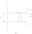
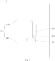
- the electronic device 1 according to the embodiments of the present disclosure will be described in detail below with reference to Figs. 1 to 5 . It should be understood that the following description is merely exemplary rather than restrictive to the present disclosure.
- the electronic device 1 in this embodiment includes: a main board 110, a cell 20, a cell protection unit 30, and a function board 120.
- the main board 110 and the function board 120 are spaced apart along a length direction of the electronic device 1, and the cell 20 is disposed between the main board 110 and the function board 120.
- the cell 20 of the electronic device 1 is not packaged.
- the cell protection unit 30 is integrated on the main board 110, that is, the cell protection unit 30 and the main board 110 form an integral structure.
- an electrode tab of the cell 20 is soldered to the main board 110, and a surface of the electrode tab of the cell 20 is provided with an adhesive layer 40.
- One end of the adhesive layer 40 extends to a surface of the cell 20, and the other end of the adhesive layer 40 extends onto the main board 110.
- the adhesive layer 40 may cover the cell protection unit 30.
- the function board 120 is electrically coupled to the cell 20 through a flexible circuit board.
- the occupied space of the cell 20 may be saved, the available space of the cell 20 may be increased, and the capacity and endurance of the cell 20 may be improved.
- the cell 20 does not need to be packaged (including various types of adhesive paper), so that the materials required for the packaging of the cell 20 may be saved, and the production cycle and cost of the cell 20 may be reduced.
- the rise in temperature during charging of the cell 20 may be improved to a certain extent, the use experience of the cell 20 may be optimized, and the production cycle of the cell 20 may be shortened.
- two cells 20 are provided in this embodiment.
- the two cells 20 are spaced apart along a width direction of the electronic device 1, and the two cells 20 are coupled in series.
- the electric capacity of the electronic device 1 may be increased, so that the standby time and operation time of the electronic device 1 may be prolonged.
- the electronic device 1 in this embodiment includes: a main board 110, a cell 20, a cell protection unit 30, and a function board 120.
- the main board 110 and the function board 120 are spaced apart along a length direction of the electronic device 1, and the cell 20 is disposed between the main board 110 and the function board 120.
- the cell 20 of the electronic device 1 is not packaged.
- the cell protection unit 30 is integrated on the function board 120, that is, the cell protection unit 30 and the function board 120 form an integral structure.
- an electrode tab of the cell 20 is soldered to the function board 120, and a surface of the electrode tab of the cell 20 is provided with an adhesive layer 40.
- One end of the adhesive layer 40 extends to a surface of the cell 20, and the other end of the adhesive layer 40 extends onto the function board 120.
- the adhesive layer 40 may cover the cell protection unit 30.
- the main board 110 is electrically coupled to the function board 120 through a flexible circuit board.
- the space of the cell may be saved, the space available for the cell 20 may be increased, and the capacity and endurance of the cell 20 may be improved.
- the cell 20 does not need to be packaged (including various types of adhesive paper), so that the materials required for the packaging of the cell 20 may be saved, and the production cycle and cost of the cell 20 may be reduced.
- the rise in temperature during charging of the cell 20 may be improved to a certain extent, the use experience of the cell 20 may be optimized, and the production cycle of the cell 20 may be shortened.
- two cells 20 are provided in this embodiment.
- the two cells 20 are spaced apart along a width direction of the electronic device 1, and the two cells 20 are coupled in series.
- the electric capacity of the electronic device 1 may be increased, so that the standby time and operating time of the electronic device 1 may be prolonged.
- first and second are used herein for purposes of description and are not intended to indicate or imply relative importance or significance or to imply the number of indicated technical features.
- the feature defined with terms “first” and “second” may explicitly or implicitly comprise one or more of the same feature.
- the term “a plurality of' means two or more than two, unless specified otherwise.
- a structure in which a first feature is "on" or “below” a second feature may include an embodiment in which the first feature is in direct contact with the second feature, and may also include an embodiment in which the first feature and the second feature are not in direct contact with each other, but are contacted via an additional feature formed therebetween.
- a first feature "on,” “above,” or “on top of' a second feature may include an embodiment in which the first feature is perpendicularly or obliquely “on,” “above,” or “on top of' the second feature, or just means that the first feature is at a height higher than that of the second feature; while a first feature “below,” “under,” or “on bottom of' a second feature may include an embodiment in which the first feature is perpendicularly or obliquely “below,” “under,” or “on bottom of' the second feature, or just means that the first feature is at a height lower than that of the second feature.
Landscapes
- Chemical & Material Sciences (AREA)
- Chemical Kinetics & Catalysis (AREA)
- Electrochemistry (AREA)
- General Chemical & Material Sciences (AREA)
- Engineering & Computer Science (AREA)
- Manufacturing & Machinery (AREA)
- Microelectronics & Electronic Packaging (AREA)
- Materials Engineering (AREA)
- Battery Mounting, Suspending (AREA)
Applications Claiming Priority (1)
| Application Number | Priority Date | Filing Date | Title |
|---|---|---|---|
| CN201910204670.8A CN111725572A (zh) | 2019-03-18 | 2019-03-18 | 电子设备 |
Publications (1)
| Publication Number | Publication Date |
|---|---|
| EP3712982A1 true EP3712982A1 (de) | 2020-09-23 |
Family
ID=70680173
Family Applications (1)
| Application Number | Title | Priority Date | Filing Date |
|---|---|---|---|
| EP20163904.4A Pending EP3712982A1 (de) | 2019-03-18 | 2020-03-18 | Elektronische vorrichtung |
Country Status (3)
| Country | Link |
|---|---|
| US (2) | US11575184B2 (de) |
| EP (1) | EP3712982A1 (de) |
| CN (1) | CN111725572A (de) |
Families Citing this family (2)
| Publication number | Priority date | Publication date | Assignee | Title |
|---|---|---|---|---|
| CN116209137A (zh) * | 2021-11-30 | 2023-06-02 | 北京小米移动软件有限公司 | 电池保护组件、电池及电池保护组件的加工方法 |
| CN222300703U (zh) * | 2023-06-15 | 2025-01-03 | 华为技术有限公司 | 电池组件及终端 |
Citations (5)
| Publication number | Priority date | Publication date | Assignee | Title |
|---|---|---|---|---|
| EP1102338A1 (de) * | 1998-05-18 | 2001-05-23 | Tyco Electronics Raychem K.K. | Ptc-element, ptc-element-montierte pcb-platte, sekundärzellenschutzkreisvorrichtung und sekundärzellenaufbau |
| US20120251849A1 (en) * | 2011-03-31 | 2012-10-04 | Samsung Sdi Co., Ltd. | Battery pack |
| EP3316384A1 (de) * | 2016-10-25 | 2018-05-02 | Samsung SDI Co., Ltd. | Batteriemodul mit einer befestigung für ein temperaturempfindliches element |
| EP3373382A1 (de) * | 2017-03-08 | 2018-09-12 | MediaTek Inc. | Verfahren zur verbesserung der temperaturverwaltung eines batteriepacks |
| EP3579300A1 (de) * | 2018-06-08 | 2019-12-11 | Samsung SDI Co., Ltd. | Batterieschutzschaltung und batteriepack damit |
Family Cites Families (13)
| Publication number | Priority date | Publication date | Assignee | Title |
|---|---|---|---|---|
| JP4168498B2 (ja) * | 1998-10-23 | 2008-10-22 | ソニー株式会社 | 非水電解質二次電池 |
| JP4949022B2 (ja) * | 2003-07-11 | 2012-06-06 | エルジー・ケム・リミテッド | 二次電池及び電池包装材 |
| JP5157338B2 (ja) * | 2006-09-21 | 2013-03-06 | 大日本印刷株式会社 | 扁平型電気化学セル金属端子部密封用接着性シート |
| CN203552132U (zh) * | 2013-10-29 | 2014-04-16 | 天津市英贝特航天科技有限公司 | 一种cpci总线加固笔记本 |
| CN105897951A (zh) * | 2014-09-22 | 2016-08-24 | 周利英 | 智能手机及其扩充模组 |
| KR102510891B1 (ko) * | 2015-11-02 | 2023-03-16 | 삼성에스디아이 주식회사 | 이차전지 |
| CN106887562B (zh) | 2015-12-15 | 2020-12-04 | 小米科技有限责任公司 | 电芯的保护主板、电子终端和电子终端用电芯的组装方法 |
| CN106207285B (zh) * | 2016-07-29 | 2019-11-15 | 北京小米移动软件有限公司 | 电池组件及智能设备 |
| CN106169787B (zh) * | 2016-09-21 | 2019-12-24 | 联想(北京)有限公司 | 一种电子设备 |
| CN106684829A (zh) * | 2017-03-17 | 2017-05-17 | 捷开通讯(深圳)有限公司 | 一种基于电子设备主板的电池保护电路以及电子设备 |
| CN108987656A (zh) * | 2017-05-31 | 2018-12-11 | 东莞新能源科技有限公司 | 电池 |
| CN208423037U (zh) * | 2018-08-13 | 2019-01-22 | Oppo广东移动通信有限公司 | 内置式电池和具有其的电子设备 |
| CN208422971U (zh) * | 2018-08-13 | 2019-01-22 | Oppo广东移动通信有限公司 | 内置式电池和具有其的电子设备 |
-
2019
- 2019-03-18 CN CN201910204670.8A patent/CN111725572A/zh active Pending
-
2020
- 2020-03-17 US US16/821,503 patent/US11575184B2/en active Active
- 2020-03-18 EP EP20163904.4A patent/EP3712982A1/de active Pending
-
2023
- 2023-01-03 US US18/092,774 patent/US11855262B2/en active Active
Patent Citations (5)
| Publication number | Priority date | Publication date | Assignee | Title |
|---|---|---|---|---|
| EP1102338A1 (de) * | 1998-05-18 | 2001-05-23 | Tyco Electronics Raychem K.K. | Ptc-element, ptc-element-montierte pcb-platte, sekundärzellenschutzkreisvorrichtung und sekundärzellenaufbau |
| US20120251849A1 (en) * | 2011-03-31 | 2012-10-04 | Samsung Sdi Co., Ltd. | Battery pack |
| EP3316384A1 (de) * | 2016-10-25 | 2018-05-02 | Samsung SDI Co., Ltd. | Batteriemodul mit einer befestigung für ein temperaturempfindliches element |
| EP3373382A1 (de) * | 2017-03-08 | 2018-09-12 | MediaTek Inc. | Verfahren zur verbesserung der temperaturverwaltung eines batteriepacks |
| EP3579300A1 (de) * | 2018-06-08 | 2019-12-11 | Samsung SDI Co., Ltd. | Batterieschutzschaltung und batteriepack damit |
Also Published As
| Publication number | Publication date |
|---|---|
| US11855262B2 (en) | 2023-12-26 |
| CN111725572A (zh) | 2020-09-29 |
| US20230148373A1 (en) | 2023-05-11 |
| US20200303714A1 (en) | 2020-09-24 |
| US11575184B2 (en) | 2023-02-07 |
Similar Documents
| Publication | Publication Date | Title |
|---|---|---|
| CN102222806B (zh) | 电池组件 | |
| CN101667664B (zh) | 保护电路组件、电池组件和用于连接这二者的方法 | |
| US11158887B2 (en) | Large-capacity secondary battery | |
| EP3291328B1 (de) | Elektrochemische sekundärbatterie mit integrierter ladeschaltung | |
| CN106207285B (zh) | 电池组件及智能设备 | |
| US20190341657A1 (en) | Smart-battery-protection plate, smart battery, and mobile platform | |
| CN111082493B (zh) | 终端设备 | |
| US11855262B2 (en) | Electronic device | |
| CN218632377U (zh) | 电池和电子设备 | |
| KR100851963B1 (ko) | 피티시소자를 탑재한 보호회로모듈을 가진 이차전지 | |
| JP2013090562A (ja) | 保護回路モジュールおよびこれを有するバッテリーパック | |
| US20100129687A1 (en) | Circuit board for secondary battery and secondary battery with the circuit board | |
| CN102082241B (zh) | 二次电池 | |
| KR101474393B1 (ko) | 배터리 팩 | |
| KR20140115756A (ko) | 배터리팩용 보호장치, 이의 제조방법 및 이를 구비한 배터리팩 | |
| EP2337108B1 (de) | Sekundärbatterie | |
| CN213150965U (zh) | 电池和使用电池的装置 | |
| CN115483508B (zh) | 电池保护板、电池组件和电子设备 | |
| KR100870356B1 (ko) | 이차전지 | |
| US9590227B2 (en) | Protection apparatus of battery pack, method of manufacturing the protection apparatus, and battery pack including the protection apparatus | |
| EP4503323A1 (de) | Batterie und elektronische vorrichtung | |
| US12255294B1 (en) | Voltage drop circuit assembly of lithium battery and 1.5V lithium battery | |
| CN222637383U (zh) | 一种电池保护板、电池及电子设备 | |
| CN223712992U (zh) | 一种电池和用电设备 | |
| CN217405649U (zh) | 电池及电子设备 |
Legal Events
| Date | Code | Title | Description |
|---|---|---|---|
| PUAI | Public reference made under article 153(3) epc to a published international application that has entered the european phase |
Free format text: ORIGINAL CODE: 0009012 |
|
| STAA | Information on the status of an ep patent application or granted ep patent |
Free format text: STATUS: THE APPLICATION HAS BEEN PUBLISHED |
|
| AK | Designated contracting states |
Kind code of ref document: A1 Designated state(s): AL AT BE BG CH CY CZ DE DK EE ES FI FR GB GR HR HU IE IS IT LI LT LU LV MC MK MT NL NO PL PT RO RS SE SI SK SM TR |
|
| AX | Request for extension of the european patent |
Extension state: BA ME |
|
| STAA | Information on the status of an ep patent application or granted ep patent |
Free format text: STATUS: REQUEST FOR EXAMINATION WAS MADE |
|
| 17P | Request for examination filed |
Effective date: 20210323 |
|
| RBV | Designated contracting states (corrected) |
Designated state(s): AL AT BE BG CH CY CZ DE DK EE ES FI FR GB GR HR HU IE IS IT LI LT LU LV MC MK MT NL NO PL PT RO RS SE SI SK SM TR |
|
| STAA | Information on the status of an ep patent application or granted ep patent |
Free format text: STATUS: EXAMINATION IS IN PROGRESS |
|
| 17Q | First examination report despatched |
Effective date: 20221019 |