EP3714518B1 - Appareil permettant de délivrer un rayonnement optique - Google Patents
Appareil permettant de délivrer un rayonnement optique Download PDFInfo
- Publication number
- EP3714518B1 EP3714518B1 EP18815781.2A EP18815781A EP3714518B1 EP 3714518 B1 EP3714518 B1 EP 3714518B1 EP 18815781 A EP18815781 A EP 18815781A EP 3714518 B1 EP3714518 B1 EP 3714518B1
- Authority
- EP
- European Patent Office
- Prior art keywords
- optical
- semiconductor amplifier
- amplifier
- input
- semiconductor
- Prior art date
- Legal status (The legal status is an assumption and is not a legal conclusion. Google has not performed a legal analysis and makes no representation as to the accuracy of the status listed.)
- Active
Links
Images




Classifications
-
- H—ELECTRICITY
- H01—ELECTRIC ELEMENTS
- H01S—DEVICES USING THE PROCESS OF LIGHT AMPLIFICATION BY STIMULATED EMISSION OF RADIATION [LASER] TO AMPLIFY OR GENERATE LIGHT; DEVICES USING STIMULATED EMISSION OF ELECTROMAGNETIC RADIATION IN WAVE RANGES OTHER THAN OPTICAL
- H01S3/00—Lasers, i.e. devices using stimulated emission of electromagnetic radiation in the infrared, visible or ultraviolet wave range
- H01S3/23—Arrangements of two or more lasers not provided for in groups H01S3/02 - H01S3/22, e.g. tandem arrangements of separate active media
- H01S3/2308—Amplifier arrangements, e.g. MOPA
-
- H—ELECTRICITY
- H01—ELECTRIC ELEMENTS
- H01S—DEVICES USING THE PROCESS OF LIGHT AMPLIFICATION BY STIMULATED EMISSION OF RADIATION [LASER] TO AMPLIFY OR GENERATE LIGHT; DEVICES USING STIMULATED EMISSION OF ELECTROMAGNETIC RADIATION IN WAVE RANGES OTHER THAN OPTICAL
- H01S3/00—Lasers, i.e. devices using stimulated emission of electromagnetic radiation in the infrared, visible or ultraviolet wave range
- H01S3/05—Construction or shape of optical resonators; Accommodation of active medium therein; Shape of active medium
- H01S3/08—Construction or shape of optical resonators or components thereof
- H01S3/081—Construction or shape of optical resonators or components thereof comprising three or more reflectors
- H01S3/0813—Configuration of resonator
- H01S3/0816—Configuration of resonator having 4 reflectors, e.g. Z-shaped resonators
-
- H—ELECTRICITY
- H01—ELECTRIC ELEMENTS
- H01S—DEVICES USING THE PROCESS OF LIGHT AMPLIFICATION BY STIMULATED EMISSION OF RADIATION [LASER] TO AMPLIFY OR GENERATE LIGHT; DEVICES USING STIMULATED EMISSION OF ELECTROMAGNETIC RADIATION IN WAVE RANGES OTHER THAN OPTICAL
- H01S3/00—Lasers, i.e. devices using stimulated emission of electromagnetic radiation in the infrared, visible or ultraviolet wave range
- H01S3/05—Construction or shape of optical resonators; Accommodation of active medium therein; Shape of active medium
- H01S3/08—Construction or shape of optical resonators or components thereof
- H01S3/081—Construction or shape of optical resonators or components thereof comprising three or more reflectors
- H01S3/083—Ring lasers
-
- H—ELECTRICITY
- H01—ELECTRIC ELEMENTS
- H01S—DEVICES USING THE PROCESS OF LIGHT AMPLIFICATION BY STIMULATED EMISSION OF RADIATION [LASER] TO AMPLIFY OR GENERATE LIGHT; DEVICES USING STIMULATED EMISSION OF ELECTROMAGNETIC RADIATION IN WAVE RANGES OTHER THAN OPTICAL
- H01S3/00—Lasers, i.e. devices using stimulated emission of electromagnetic radiation in the infrared, visible or ultraviolet wave range
- H01S3/10—Controlling the intensity, frequency, phase, polarisation or direction of the emitted radiation, e.g. switching, gating, modulating or demodulating
- H01S3/13—Stabilisation of laser output parameters, e.g. frequency or amplitude
- H01S3/1305—Feedback control systems
-
- H—ELECTRICITY
- H01—ELECTRIC ELEMENTS
- H01S—DEVICES USING THE PROCESS OF LIGHT AMPLIFICATION BY STIMULATED EMISSION OF RADIATION [LASER] TO AMPLIFY OR GENERATE LIGHT; DEVICES USING STIMULATED EMISSION OF ELECTROMAGNETIC RADIATION IN WAVE RANGES OTHER THAN OPTICAL
- H01S3/00—Lasers, i.e. devices using stimulated emission of electromagnetic radiation in the infrared, visible or ultraviolet wave range
- H01S3/10—Controlling the intensity, frequency, phase, polarisation or direction of the emitted radiation, e.g. switching, gating, modulating or demodulating
- H01S3/13—Stabilisation of laser output parameters, e.g. frequency or amplitude
- H01S3/131—Stabilisation of laser output parameters, e.g. frequency or amplitude by controlling the active medium, e.g. by controlling the processes or apparatus for excitation
- H01S3/1315—Stabilisation of laser output parameters, e.g. frequency or amplitude by controlling the active medium, e.g. by controlling the processes or apparatus for excitation by gain saturation
-
- H—ELECTRICITY
- H01—ELECTRIC ELEMENTS
- H01S—DEVICES USING THE PROCESS OF LIGHT AMPLIFICATION BY STIMULATED EMISSION OF RADIATION [LASER] TO AMPLIFY OR GENERATE LIGHT; DEVICES USING STIMULATED EMISSION OF ELECTROMAGNETIC RADIATION IN WAVE RANGES OTHER THAN OPTICAL
- H01S3/00—Lasers, i.e. devices using stimulated emission of electromagnetic radiation in the infrared, visible or ultraviolet wave range
- H01S3/10—Controlling the intensity, frequency, phase, polarisation or direction of the emitted radiation, e.g. switching, gating, modulating or demodulating
- H01S3/13—Stabilisation of laser output parameters, e.g. frequency or amplitude
- H01S3/136—Stabilisation of laser output parameters, e.g. frequency or amplitude by controlling devices placed within the cavity
-
- H—ELECTRICITY
- H01—ELECTRIC ELEMENTS
- H01S—DEVICES USING THE PROCESS OF LIGHT AMPLIFICATION BY STIMULATED EMISSION OF RADIATION [LASER] TO AMPLIFY OR GENERATE LIGHT; DEVICES USING STIMULATED EMISSION OF ELECTROMAGNETIC RADIATION IN WAVE RANGES OTHER THAN OPTICAL
- H01S3/00—Lasers, i.e. devices using stimulated emission of electromagnetic radiation in the infrared, visible or ultraviolet wave range
- H01S3/14—Lasers, i.e. devices using stimulated emission of electromagnetic radiation in the infrared, visible or ultraviolet wave range characterised by the material used as the active medium
- H01S3/16—Solid materials
- H01S3/163—Solid materials characterised by a crystal matrix
- H01S3/1666—Solid materials characterised by a crystal matrix borate, carbonate, arsenide
-
- H—ELECTRICITY
- H01—ELECTRIC ELEMENTS
- H01S—DEVICES USING THE PROCESS OF LIGHT AMPLIFICATION BY STIMULATED EMISSION OF RADIATION [LASER] TO AMPLIFY OR GENERATE LIGHT; DEVICES USING STIMULATED EMISSION OF ELECTROMAGNETIC RADIATION IN WAVE RANGES OTHER THAN OPTICAL
- H01S5/00—Semiconductor lasers
- H01S5/50—Amplifier structures not provided for in groups H01S5/02 - H01S5/30
- H01S5/5009—Amplifier structures not provided for in groups H01S5/02 - H01S5/30 the arrangement being polarisation-insensitive
- H01S5/5018—Amplifier structures not provided for in groups H01S5/02 - H01S5/30 the arrangement being polarisation-insensitive using two or more amplifiers or multiple passes through the same amplifier
-
- H—ELECTRICITY
- H01—ELECTRIC ELEMENTS
- H01S—DEVICES USING THE PROCESS OF LIGHT AMPLIFICATION BY STIMULATED EMISSION OF RADIATION [LASER] TO AMPLIFY OR GENERATE LIGHT; DEVICES USING STIMULATED EMISSION OF ELECTROMAGNETIC RADIATION IN WAVE RANGES OTHER THAN OPTICAL
- H01S2301/00—Functional characteristics
- H01S2301/03—Suppression of nonlinear conversion, e.g. specific design to suppress for example stimulated brillouin scattering [SBS], mainly in optical fibres in combination with multimode pumping
-
- H—ELECTRICITY
- H01—ELECTRIC ELEMENTS
- H01S—DEVICES USING THE PROCESS OF LIGHT AMPLIFICATION BY STIMULATED EMISSION OF RADIATION [LASER] TO AMPLIFY OR GENERATE LIGHT; DEVICES USING STIMULATED EMISSION OF ELECTROMAGNETIC RADIATION IN WAVE RANGES OTHER THAN OPTICAL
- H01S3/00—Lasers, i.e. devices using stimulated emission of electromagnetic radiation in the infrared, visible or ultraviolet wave range
- H01S3/05—Construction or shape of optical resonators; Accommodation of active medium therein; Shape of active medium
- H01S3/06—Construction or shape of active medium
- H01S3/063—Waveguide lasers, i.e. whereby the dimensions of the waveguide are of the order of the light wavelength
- H01S3/067—Fibre lasers
- H01S3/06708—Constructional details of the fibre, e.g. compositions, cross-section, shape or tapering
- H01S3/06712—Polarising fibre; Polariser
-
- H—ELECTRICITY
- H01—ELECTRIC ELEMENTS
- H01S—DEVICES USING THE PROCESS OF LIGHT AMPLIFICATION BY STIMULATED EMISSION OF RADIATION [LASER] TO AMPLIFY OR GENERATE LIGHT; DEVICES USING STIMULATED EMISSION OF ELECTROMAGNETIC RADIATION IN WAVE RANGES OTHER THAN OPTICAL
- H01S3/00—Lasers, i.e. devices using stimulated emission of electromagnetic radiation in the infrared, visible or ultraviolet wave range
- H01S3/05—Construction or shape of optical resonators; Accommodation of active medium therein; Shape of active medium
- H01S3/06—Construction or shape of active medium
- H01S3/063—Waveguide lasers, i.e. whereby the dimensions of the waveguide are of the order of the light wavelength
- H01S3/067—Fibre lasers
- H01S3/06754—Fibre amplifiers
- H01S3/06758—Tandem amplifiers
Definitions
- Lasers such as fibre lasers and disk lasers have important applications for marking, cutting, scribing, welding, additive manufacturing, and other industrial processing of materials.
- the lasers are used in many industries including consumer electronics, medical devices, automotive, and aerospace.
- the lasers can be pulsed or continuous wave. Typical pulse lengths that are achievable range from a few picoseconds through nanoseconds, microseconds and milliseconds.
- the pulse repetition rate is controlled electronically and can be varied over a wide range.
- non-linear effects for example, spectral noise, temporal noise, speckle, non-linear wavelength conversion of the optical radiation, and self Q-switching.
- spectral noise for example, spectral noise, temporal noise, speckle
- non-linear wavelength conversion of the optical radiation for example, spectral noise, temporal noise, speckle
- non-linear wavelength conversion of the optical radiation for example, spectral noise, temporal noise, speckle
- non-linear wavelength conversion causes errors in optical focussing systems and can reduce the optical power able to be delivered to a material
- self Q-switching can destroy optical amplifiers and optical fibres in the laser system.
- a partial solution is to use a superluminescent diode as a seed laser in a master oscillator power amplifier in order to increase the bandwidth of the optical radiation and thus reduced the onset of non-linear effects.
- This solution has allowed power levels to be increased. However, as the power level is increased further, the power amplifier can suffer from non-linear effects. Moreover, the superluminescent diode can start to emit coherent laser radiation, that is, the superluminescent diode can start to lase. This further exacerbates non-linear effects in the power amplifier and in optical fibre delivery systems, and can lead to catastrophic failure of the power amplifier and optical fibre delivery system.
- non-linear effects include spectral noise, temporal noise, speckle, non-linear wavelength conversion of the optical radiation, and self Q-switching.
- the resonant cavity may operate to provide optical feedback in the form of the input optical radiation
- the first semiconductor amplifier may be configured to supply optical radiation to the preamplifier in the event that the optical feedback is lost in order to prevent catastrophic failure of the power amplifier.
- the first semiconductor amplifier it is possible to operate the first semiconductor amplifier at intensity levels that would normally cause it to be unstable or lase. This is achieved by optically injecting optical radiation from an optical source which is then amplified by the first semiconductor amplifier in a double pass configuration, and then output via the output fibre.
- the power of the input optical radiation is selected such that the first semiconductor amplifier does not lase.
- the power of the input optical radiation is preferably greater than the power of reflections that make the first semiconductor amplifier lase at the optical lasing threshold.
- the resonant cavity operates through non-linear optical effects that are highly dependent on the instantaneous optical power and instantaneous wavelength of the output radiation.
- Operating the first semiconductor amplifier in saturation reduces the spectral noise, temporal noise, and non-linear wavelength conversion of the output radiation, which therefore results in a far more stable operation of the resonant cavity and thus a lower noise and more stable frequency converted radiation.
- Such a configuration can also help reduce catastrophic failure of the ring laser in the event that feedback from the resonant cavity is lost, particularly when setting up and aligning the apparatus. This is because the first semiconductor amplifier can be configured to output optical radiation in the absence of the optical radiation provided by the optical source.
- the apparatus may include an optical isolator between the preamplifier and the power amplifier.
- the apparatus may comprise an optical filter between the optical input and the first semiconductor amplifier.
- the coupler may be an optical circulator.
- the apparatus may comprise an optical isolator between the coupler and the preamplifier.
- the method may comprise the steps of causing the resonant cavity to provide optical feedback in the form of the input optical radiation, and configuring the first semiconductor amplifier to supply optical radiation to the preamplifier in the event that the optical feedback is lost in order to prevent catastrophic failure of the power amplifier.
- the method may include the steps of using a detector to detect for an absence of the input optical radiation, and reducing an optical gain of the first semiconductor amplifier in order to prevent the first semiconductor amplifier from lasing.
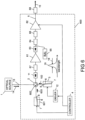
- a coupler 64 can be provided between the preamplifier 61 and the power amplifier 62 which is connected to a visible light source 65.
- the visible light source 65 can be a laser diode, a superluminescent diode, or a light emitting diode.
- the visible light source 65 is useful for alignment purposes, for example, when setting up laser marking, laser, welding, or laser cutting systems.
- the visible light source 65 preferably has a wavelength of between 500nm and 670nm, and more preferably between 600nm and 670nm.
- the coupler 64 is preferably a wavelength division multiplexer connected to the visible light source 65 and the preamplifier 61 at its inputs, and the power amplifier 62 at its output.
- the mid-stage isolator 63 if present, is preferably located between the preamplifier 61 and the coupler 64.
- configuring the optical source 1 to be a superluminescent diode, and using the superluminescent diode to seed the first semiconductor amplifier 3 allowed the first semiconductor amplifier 3 to be operated at output powers 21 greater than two, and preferably greater than three times its optical lasing threshold 28.
- This is a surprising result that enables the optical power of the optical radiation 15 to be increased without requiring an additional optical-fibre amplification stage. Without intending to limit the scope of the invention, it is believed that this is because the first semiconductor amplifier 3 is being operated in saturation with respect to the input optical radiation 14, and thus has a lower small signal gain than when the input optical radiation 14 is not present. Therefore the optical lasing threshold 28 of the first semiconductor amplifier 3 is increased, allowing output powers 21 greater than the optical lasing threshold 28 to be achieved.
- the controller 4 preferably controls the optical source 1 and the first semiconductor amplifier 3 in synchronism with each other.
- the controller 4 turns the optical source 1 on before the first semiconductor amplifier 3.
- the controller 4 can also be connected to at least one of the preamplifier 61 and the power amplifier 62.
- At least one of the preamplifier 61 and the power amplifier 62 can be controlled in synchronism with the first semiconductor amplifier 3, and can be turned on before the controller 4 turns the first semiconductor amplifier 3 on. This can be advantageous in order to improve the turn on characteristics of the optical radiation 15, such as rise time and pulse to pulse variation of output pulses.
- the apparatus shown in Figure 1 has an optical filter 9 between the optical source 1 and the first semiconductor amplifier 3.
- the optical filter 9 can be an etalon filter, a fibre Bragg grating, a thin film filter, or any other suitable type of optical filter.
- the optical filter 9 can be tuneable.
- the optical filter 9 can be an acoustic-optically tuneable filter.
- the optical filter 9 is selected to reduce the optical bandwidth of the optical source 1 in order to optimize the performance of the apparatus.
- the optical filter 9 can have a bandwidth of 10nm in order to reduce the likelihood of stimulated Brillouin scattering and / or stimulated Raman scattering.
- the optical source 1 can be a fibre laser, a source of amplified spontaneous emission radiation which preferably comprises a rare-earth doped optical fibre, or a random fibre laser.
- the random fibre laser can comprise a half open cavity comprising 100m or more of passive optical fibre connected to an active optical fibre having an optical reflector at its output end. Such an arrangement is described in IEEE Journal of Selected Topics in Quantum Electronics, Volume 21(1), pages 10-15, 2015 .
- a problem that can occur with the apparatus 100 of Figure 1 is that in the absence of the input optical radiation 14, the first semiconductor amplifier 3 can lase. This can result in non-linear effects arising in the preamplifier 61, power amplifier 62 and the optical fibre 5 such as stimulated Brillouin scattering. Stimulated Brillouin scattering can cause self Q-switching, and / or catastrophic failure of the apparatus 100.
- the saturable absorber 72 is shown prior to the preamplifier 61 to filter out optical noise that can occur between the optical pulses 75.
- the saturable absorber 72 can be a semiconductor saturable absorber such as an SA-1064-14-500fs-FC/APC saturable absorber supplied by Batop GmbH of Jena, Germany.
- the saturable absorber 72 may comprise a quantum well microcavity, graphene, carbon nanotubes, or may be an optical fibre doped with a rare earth or a semiconductor.
- the saturable absorber 72 can also be used in the apparatus shown in Figures 1 and 6 .
- the mode locked laser 71 can a semiconductor mode locked laser, or a fibre mode locked laser.
- the mode locked laser 71 can be a picosecond mode-locked laser, or a femtosecond mode locked laser.
Landscapes
- Physics & Mathematics (AREA)
- Electromagnetism (AREA)
- Engineering & Computer Science (AREA)
- Optics & Photonics (AREA)
- Plasma & Fusion (AREA)
- Chemical & Material Sciences (AREA)
- Crystallography & Structural Chemistry (AREA)
- Automation & Control Theory (AREA)
- General Physics & Mathematics (AREA)
- Condensed Matter Physics & Semiconductors (AREA)
- Semiconductor Lasers (AREA)
- Lasers (AREA)
- Optical Modulation, Optical Deflection, Nonlinear Optics, Optical Demodulation, Optical Logic Elements (AREA)
Claims (15)
- Appareil permettant de délivrer un rayonnement optique, ledit appareil comprenant une entrée optique (14), un coupleur (2), un premier amplificateur à semiconducteurs (3), un dispositif de commande (4), un préamplificateur (61), un amplificateur de puissance (62), une fibre de sortie (5) et une cavité résonnante (624),• l'entrée optique servant à recevoir un rayonnement optique d'entrée (14) ;• l'entrée optique étant connectée en série au coupleur, au premier amplificateur à semiconducteurs, au préamplificateur, à l'amplificateur de puissance, à la fibre de sortie et à la cavité résonante ;• la cavité résonante comprenant un cristal non linéaire (628) ;l'appareil étant caractérisé en ce que :• la cavité résonante est connectée à l'entrée optique, ce qui permet de former un laser en anneau comprenant le coupleur, le premier amplificateur à semiconducteurs, le préamplificateur, l'amplificateur de puissance, la fibre de sortie et la cavité résonante ;• le premier amplificateur à semiconducteurs comprend un guide d'ondes ayant une facette à faible réflexion ;• le premier amplificateur à semiconducteurs est dans une configuration à double passage de telle sorte que la facette à faible réflexion soit connectée à la fois à l'entrée optique et au préamplificateur par l'intermédiaire du coupleur ;• le dispositif de commande est configuré pour amener le guide d'ondes du premier amplificateur à semiconducteurs à fonctionner en saturation, ce qui permet au premier amplificateur à semiconducteurs de réduire des effets non linéaires dans le préamplificateur, l'amplificateur de puissance et la fibre de sortie.
- Appareil selon la revendication 1, dans lequel la cavité résonnante fonctionne pour fournir un retour optique sous la forme du rayonnement optique d'entrée, et le premier amplificateur à semiconducteurs est configuré pour délivrer un rayonnement optique au préamplificateur dans le cas où le retour optique est perdu afin d'éviter une panne catastrophique de l'amplificateur de puissance.
- Appareil selon la revendication 1 ou 2, dans lequel le dispositif de commande et le premier amplificateur à semiconducteurs sont tels que le premier amplificateur à semiconducteurs émet une lumière laser en l'absence du rayonnement optique d'entrée et qu'il est empêché au premier amplificateur à semiconducteurs d'émettre une lumière laser par la présence du rayonnement optique d'entrée.
- Appareil selon la revendication 1 ou 2, dans lequel le dispositif de commande est configuré pour commander un gain optique du premier amplificateur à semiconducteurs de telle sorte que le gain optique soit réduit en l'absence du rayonnement optique d'entrée, ce qui empêche le premier amplificateur à semiconducteurs d'émettre une lumière laser.
- Appareil selon l'une quelconque des revendications précédentes, dans lequel le guide d'ondes du premier amplificateur à semiconducteurs est un guide d'ondes incurvé, ce qui permet d'atteindre des puissances plus élevées dans le rayonnement optique.
- Appareil selon l'une quelconque des revendications précédentes, comprenant un atténuateur optique situé entre l'entrée optique et le coupleur.
- Appareil selon la revendication 6, dans lequel le dispositif de commande règle l'atténuateur optique de telle sorte que le premier amplificateur à semiconducteurs fonctionne en saturation.
- Appareil selon l'une quelconque des revendications précédentes, comprenant un isolateur optique entre le préamplificateur et l'amplificateur de puissance.
- Appareil selon l'une quelconque des revendications précédentes, comprenant un filtre optique entre l'entrée optique et le premier amplificateur à semiconducteurs.
- Appareil selon l'une quelconque des revendications précédentes, comprenant un isolateur optique entre l'entrée optique et le coupleur.
- Appareil selon l'une quelconque des revendications précédentes, dans lequel le coupleur est un circulateur optique.
- Appareil selon l'une quelconque des revendications précédentes, comprenant un isolateur optique entre le coupleur et le préamplificateur.
- Procédé permettant de délivrer un rayonnement optique, ledit procédé consistant à :• fournir une entrée optique, un coupleur, un premier amplificateur à semiconducteurs, un préamplificateur, un amplificateur de puissance, une fibre de sortie et une cavité résonante qui sont configurés en série ;• situer un cristal non linéaire dans la cavité résonante ;• amplifier le rayonnement optique d'entrée reçu par l'entrée optique par le premier amplificateur à semiconducteurs, le préamplificateur et l'amplificateur de puissance ; et• délivrer en sortie le rayonnement optique par l'amplificateur de puissance par l'intermédiaire d'une fibre de sortie ;le procédé étant caractérisé par les étapes consistant à :• former un laser en anneau en connectant la cavité résonnante à l'entrée optique ;• configurer un dispositif de commande pour amener le guide d'ondes à fonctionner en saturation, ce qui permet de réduire un bruit spectral et/ou un bruit temporel et/ou une conversion non linéaire de longueur d'onde du rayonnement optique,où :• le premier amplificateur à semiconducteurs comprend un guide d'ondes ayant une facette à faible réflexion ;• le premier amplificateur à semiconducteurs est dans une configuration à double passage de telle sorte que la facette à faible réflexion soit connectée à la fois à l'entrée optique et au préamplificateur par l'intermédiaire du coupleur.
- Procédé selon la revendication 13, comprenant les étapes consistant à amener la cavité résonnante à fournir un retour optique sous la forme du rayonnement optique d'entrée, et à configurer le premier amplificateur à semiconducteurs pour délivrer un rayonnement optique au préamplificateur dans le cas où le retour optique est perdu afin d'éviter une panne catastrophique de l'amplificateur de puissance.
- Procédé selon la revendication 13 ou 14, comprenant les étapes consistant à utiliser un détecteur pour détecter une absence du rayonnement optique d'entrée et à réduire un gain optique du premier amplificateur à semiconducteurs afin d'empêcher le premier amplificateur à semiconducteurs d'émettre une lumière laser.
Applications Claiming Priority (2)
| Application Number | Priority Date | Filing Date | Title |
|---|---|---|---|
| GBGB1719629.6A GB201719629D0 (en) | 2017-11-24 | 2017-11-24 | Apparatus for providing optical radiation |
| PCT/GB2018/000149 WO2019102174A2 (fr) | 2017-11-24 | 2018-11-23 | Appareil permettant de délivrer un rayonnement optique |
Publications (2)
| Publication Number | Publication Date |
|---|---|
| EP3714518A2 EP3714518A2 (fr) | 2020-09-30 |
| EP3714518B1 true EP3714518B1 (fr) | 2024-07-03 |
Family
ID=60950733
Family Applications (1)
| Application Number | Title | Priority Date | Filing Date |
|---|---|---|---|
| EP18815781.2A Active EP3714518B1 (fr) | 2017-11-24 | 2018-11-23 | Appareil permettant de délivrer un rayonnement optique |
Country Status (5)
| Country | Link |
|---|---|
| US (1) | US11569633B2 (fr) |
| EP (1) | EP3714518B1 (fr) |
| CN (2) | CN208986366U (fr) |
| GB (1) | GB201719629D0 (fr) |
| WO (1) | WO2019102174A2 (fr) |
Families Citing this family (12)
| Publication number | Priority date | Publication date | Assignee | Title |
|---|---|---|---|---|
| GB201719629D0 (en) * | 2017-11-24 | 2018-01-10 | Spi Lasers Uk Ltd | Apparatus for providing optical radiation |
| US11527059B2 (en) * | 2020-01-28 | 2022-12-13 | International Business Machines Corporation | Reservoir computing |
| IT202000001897A1 (it) * | 2020-01-31 | 2021-07-31 | Univ Degli Studi Di Trento | Dispositivo laser a guadagno interferometrico |
| CN114079603B (zh) * | 2020-08-13 | 2023-08-22 | 华为技术有限公司 | 一种信号折叠方法及设备 |
| JPWO2022107397A1 (fr) * | 2020-11-20 | 2022-05-27 | ||
| US11555958B2 (en) * | 2021-04-01 | 2023-01-17 | Saudi Arabian Oil Company | Nested anti-resonant nodeless optical fiber and subsurface system using the same |
| US12429701B2 (en) | 2021-12-13 | 2025-09-30 | Samsung Electronics Co., Ltd. | Augmented reality device based on curved waveguide, method therefor, augmented reality glasses based on said device |
| CN114976838B (zh) * | 2022-05-16 | 2024-08-02 | 电子科技大学 | 基于超低损耗光纤的超长距离高阶随机光纤激光器及传感器 |
| CN115394883A (zh) * | 2022-09-30 | 2022-11-25 | 中国电子科技集团公司第四十四研究所 | 基于量子阱及量子点混合有源区的超宽谱高增益饱和增益芯片 |
| CN115549778B (zh) * | 2022-09-30 | 2024-11-01 | 长春理工大学 | 多通道航天级光前置放大器辐照环境测试装置 |
| CN116845677B (zh) * | 2023-07-03 | 2024-01-26 | 中国人民解放军国防科技大学 | 一种基于随机分布式反馈的单级高功率超连续谱光源 |
| CN117220127B (zh) * | 2023-11-07 | 2024-03-19 | 中国工程物理研究院激光聚变研究中心 | 一种抑制受激拉曼散射的光纤激光器及其参数优化方法 |
Citations (1)
| Publication number | Priority date | Publication date | Assignee | Title |
|---|---|---|---|---|
| US8520306B2 (en) * | 2008-10-24 | 2013-08-27 | Spi Lasers Uk Ltd | Apparatus for combining laser radiation |
Family Cites Families (24)
| Publication number | Priority date | Publication date | Assignee | Title |
|---|---|---|---|---|
| JP3137632B2 (ja) * | 1989-08-31 | 2001-02-26 | 富士通株式会社 | 光ファイバ増幅器を備えた光通信方式 |
| WO1993018561A1 (fr) | 1992-03-13 | 1993-09-16 | Raychem Corporation | Amplificateur optique pompe par laser annulaire |
| US5920588A (en) * | 1996-04-11 | 1999-07-06 | Fujitsu Limited | Method and device for generation of phase conjugate light and wavelength conversion, and system having the device |
| US6151338A (en) * | 1997-02-19 | 2000-11-21 | Sdl, Inc. | High power laser optical amplifier system |
| US6314117B1 (en) * | 1998-12-16 | 2001-11-06 | Quan Photonics, Inc | Laser diode package |
| JP2000310800A (ja) * | 1999-02-23 | 2000-11-07 | Atr Adaptive Communications Res Lab | 2光信号発生器 |
| JP4689008B2 (ja) * | 2000-07-04 | 2011-05-25 | 富士通株式会社 | 信号光を波形整形するための方法及び装置 |
| US6456429B1 (en) | 2000-11-15 | 2002-09-24 | Onetta, Inc. | Double-pass optical amplifier |
| US6940880B2 (en) * | 2003-03-11 | 2005-09-06 | Coherent, Inc. | Optically pumped semiconductor ring laser |
| US7443903B2 (en) * | 2006-04-19 | 2008-10-28 | Mobius Photonics, Inc. | Laser apparatus having multiple synchronous amplifiers tied to one master oscillator |
| CN101063731A (zh) * | 2006-04-30 | 2007-10-31 | 深圳大学 | 分布式反馈抑制半导体光放大器 |
| EP2016652B1 (fr) * | 2006-05-11 | 2014-06-18 | SPI Lasers UK Limited | Appareil de rayonnement optique |
| US20080018988A1 (en) | 2006-07-24 | 2008-01-24 | Andrew Davidson | Light source with tailored output spectrum |
| US20090296759A1 (en) | 2008-06-03 | 2009-12-03 | Andrei Starodoumov | Sequentially-modulated diode-laser seed-pulse generator |
| US20100027571A1 (en) * | 2008-07-31 | 2010-02-04 | Murdoch Keith M | Stabilized near-infrared laser |
| US8593725B2 (en) | 2009-08-04 | 2013-11-26 | Jds Uniphase Corporation | Pulsed optical source |
| CN107017555B (zh) * | 2010-01-08 | 2018-11-06 | Ii-Vi 激光企业有限责任公司 | 具有高线性度输出的激光系统 |
| DE102011075213B4 (de) * | 2011-05-04 | 2013-02-21 | Trumpf Laser Gmbh + Co. Kg | Laserbearbeitungssystem mit einem in seiner Brillanz einstellbaren Bearbeitungslaserstrahl |
| CN102637990A (zh) * | 2012-04-25 | 2012-08-15 | 清华大学 | 一种光纤放大系统及其光纤放大方法 |
| US9158057B2 (en) | 2012-05-18 | 2015-10-13 | Gerard A Alphonse | Semiconductor light source free from facet reflections |
| CN102749785A (zh) * | 2012-07-26 | 2012-10-24 | 浙江师范大学 | 双泵浦傅立叶域锁模光纤光学参量振荡器 |
| CN203826765U (zh) * | 2014-04-23 | 2014-09-10 | 上海朗研光电科技有限公司 | 一种偏振自动稳定控制的全光纤级联激光放大装置 |
| CN105428998B (zh) * | 2015-12-28 | 2019-05-17 | 中国科学院半导体研究所 | 外腔窄线宽激光器 |
| GB201719629D0 (en) * | 2017-11-24 | 2018-01-10 | Spi Lasers Uk Ltd | Apparatus for providing optical radiation |
-
2017
- 2017-11-24 GB GBGB1719629.6A patent/GB201719629D0/en not_active Ceased
-
2018
- 2018-11-23 US US16/762,527 patent/US11569633B2/en active Active
- 2018-11-23 EP EP18815781.2A patent/EP3714518B1/fr active Active
- 2018-11-23 WO PCT/GB2018/000149 patent/WO2019102174A2/fr not_active Ceased
- 2018-11-23 CN CN201821961584.9U patent/CN208986366U/zh active Active
- 2018-11-23 CN CN201880075871.6A patent/CN111373614B/zh active Active
Patent Citations (1)
| Publication number | Priority date | Publication date | Assignee | Title |
|---|---|---|---|---|
| US8520306B2 (en) * | 2008-10-24 | 2013-08-27 | Spi Lasers Uk Ltd | Apparatus for combining laser radiation |
Also Published As
| Publication number | Publication date |
|---|---|
| CN111373614B (zh) | 2023-08-01 |
| WO2019102174A2 (fr) | 2019-05-31 |
| GB201719629D0 (en) | 2018-01-10 |
| EP3714518A2 (fr) | 2020-09-30 |
| US20200280164A1 (en) | 2020-09-03 |
| US11569633B2 (en) | 2023-01-31 |
| CN111373614A (zh) | 2020-07-03 |
| WO2019102174A3 (fr) | 2019-06-20 |
| CN208986366U (zh) | 2019-06-14 |
Similar Documents
| Publication | Publication Date | Title |
|---|---|---|
| US11569633B2 (en) | Apparatus for providing optical radiation | |
| JP3567233B2 (ja) | 高エネルギーレベルを有する高ピークパワーを供給する光増幅器 | |
| US9819141B2 (en) | Compact fiber short pulse laser sources | |
| US9923329B2 (en) | Q-switched oscillator seed-source for MOPA laser illuminator apparatus and method | |
| US20090003391A1 (en) | Low-repetition-rate ring-cavity passively mode-locked fiber laser | |
| US7457329B2 (en) | Method and system for a high power low-coherence pulsed light source | |
| JP2013077831A (ja) | モジュール式ファイバ型チャープパルス増幅システム | |
| KR19980022444A (ko) | 수동형 모드록킹 광섬유 레이저 구조 | |
| CN101517848A (zh) | 用于提供光辐射的设备 | |
| WO2007044789A2 (fr) | Appareil et methode pour generer de courtes impulsions optiques | |
| CN109149336B (zh) | 基于sbs和法布里珀罗干涉仪的被动调q锁模激光器 | |
| CN104466636A (zh) | 一种单频调q脉冲光纤激光器 | |
| WO2019053487A1 (fr) | Laser ou amplificateur optique stabilisé et procédé de stabilisation | |
| Vazquez-Zuniga et al. | Wavelength-tunable, passively mode-locked erbium-doped fiber master-oscillator incorporating a semiconductor saturable absorber mirror | |
| Frankel et al. | Rapid continuous tuning of a single-polarization fiber ring laser | |
| CN109560453B (zh) | 基于sbs和法布里珀罗干涉仪的被动调q锁模环形激光器 | |
| US9172203B2 (en) | Laser system for the marking of metallic and non-metallic materials | |
| US8014428B2 (en) | Mode-locked laser | |
| Huang et al. | Fiber-grating-based self-matched additive-pulse mode-locked fiber lasers | |
| Gutty et al. | kW-level tunable Q-switched thulium-doped fiber system | |
| Motard et al. | Continuous Wave and Pulsed Modes of Operation of a High Power 2.09 µm Monolithic Single Oscillator Tm3+, Ho3+-Codoped Fiber Laser | |
| Chernikov et al. | Q-switching of Er/sup 3+//Yb/sup 3+/-doped fiber laser using backscattering from a fiber ring interferometer | |
| WO2008074359A1 (fr) | Laser à fibre optique | |
| Ismail et al. | Multi-wavelength Brillouin Raman Erbium Fiber Laser utilizing Captured Residual Raman Pump Power | |
| CN114696191A (zh) | 一种实现多波长锁模亮暗脉冲的装置及方法 |
Legal Events
| Date | Code | Title | Description |
|---|---|---|---|
| STAA | Information on the status of an ep patent application or granted ep patent |
Free format text: STATUS: UNKNOWN |
|
| STAA | Information on the status of an ep patent application or granted ep patent |
Free format text: STATUS: THE INTERNATIONAL PUBLICATION HAS BEEN MADE |
|
| PUAI | Public reference made under article 153(3) epc to a published international application that has entered the european phase |
Free format text: ORIGINAL CODE: 0009012 |
|
| STAA | Information on the status of an ep patent application or granted ep patent |
Free format text: STATUS: REQUEST FOR EXAMINATION WAS MADE |
|
| 17P | Request for examination filed |
Effective date: 20200514 |
|
| AK | Designated contracting states |
Kind code of ref document: A2 Designated state(s): AL AT BE BG CH CY CZ DE DK EE ES FI FR GB GR HR HU IE IS IT LI LT LU LV MC MK MT NL NO PL PT RO RS SE SI SK SM TR |
|
| AX | Request for extension of the european patent |
Extension state: BA ME |
|
| RIN1 | Information on inventor provided before grant (corrected) |
Inventor name: DURKIN, MICHAEL KEVAN Inventor name: ALMEIDA, PAULO Inventor name: CODEMARD, CHRISTOPHE ANDRE |
|
| DAV | Request for validation of the european patent (deleted) | ||
| DAX | Request for extension of the european patent (deleted) | ||
| GRAP | Despatch of communication of intention to grant a patent |
Free format text: ORIGINAL CODE: EPIDOSNIGR1 |
|
| STAA | Information on the status of an ep patent application or granted ep patent |
Free format text: STATUS: GRANT OF PATENT IS INTENDED |
|
| INTG | Intention to grant announced |
Effective date: 20240207 |
|
| GRAS | Grant fee paid |
Free format text: ORIGINAL CODE: EPIDOSNIGR3 |
|
| GRAJ | Information related to disapproval of communication of intention to grant by the applicant or resumption of examination proceedings by the epo deleted |
Free format text: ORIGINAL CODE: EPIDOSDIGR1 |
|
| GRAL | Information related to payment of fee for publishing/printing deleted |
Free format text: ORIGINAL CODE: EPIDOSDIGR3 |
|
| STAA | Information on the status of an ep patent application or granted ep patent |
Free format text: STATUS: REQUEST FOR EXAMINATION WAS MADE |
|
| RAP3 | Party data changed (applicant data changed or rights of an application transferred) |
Owner name: TRUMPF LASER UK LIMITED |
|
| INTC | Intention to grant announced (deleted) | ||
| GRAP | Despatch of communication of intention to grant a patent |
Free format text: ORIGINAL CODE: EPIDOSNIGR1 |
|
| STAA | Information on the status of an ep patent application or granted ep patent |
Free format text: STATUS: GRANT OF PATENT IS INTENDED |
|
| GRAS | Grant fee paid |
Free format text: ORIGINAL CODE: EPIDOSNIGR3 |
|
| GRAA | (expected) grant |
Free format text: ORIGINAL CODE: 0009210 |
|
| STAA | Information on the status of an ep patent application or granted ep patent |
Free format text: STATUS: THE PATENT HAS BEEN GRANTED |
|
| INTG | Intention to grant announced |
Effective date: 20240522 |
|
| AK | Designated contracting states |
Kind code of ref document: B1 Designated state(s): AL AT BE BG CH CY CZ DE DK EE ES FI FR GB GR HR HU IE IS IT LI LT LU LV MC MK MT NL NO PL PT RO RS SE SI SK SM TR |
|
| REG | Reference to a national code |
Ref country code: CH Ref legal event code: EP |
|
| REG | Reference to a national code |
Ref country code: DE Ref legal event code: R096 Ref document number: 602018071368 Country of ref document: DE |
|
| REG | Reference to a national code |
Ref country code: LT Ref legal event code: MG9D |
|
| REG | Reference to a national code |
Ref country code: NL Ref legal event code: MP Effective date: 20240703 |
|
| PG25 | Lapsed in a contracting state [announced via postgrant information from national office to epo] |
Ref country code: PT Free format text: LAPSE BECAUSE OF FAILURE TO SUBMIT A TRANSLATION OF THE DESCRIPTION OR TO PAY THE FEE WITHIN THE PRESCRIBED TIME-LIMIT Effective date: 20241104 |
|
| REG | Reference to a national code |
Ref country code: AT Ref legal event code: MK05 Ref document number: 1700826 Country of ref document: AT Kind code of ref document: T Effective date: 20240703 |
|
| PG25 | Lapsed in a contracting state [announced via postgrant information from national office to epo] |
Ref country code: NL Free format text: LAPSE BECAUSE OF FAILURE TO SUBMIT A TRANSLATION OF THE DESCRIPTION OR TO PAY THE FEE WITHIN THE PRESCRIBED TIME-LIMIT Effective date: 20240703 |
|
| PG25 | Lapsed in a contracting state [announced via postgrant information from national office to epo] |
Ref country code: PT Free format text: LAPSE BECAUSE OF FAILURE TO SUBMIT A TRANSLATION OF THE DESCRIPTION OR TO PAY THE FEE WITHIN THE PRESCRIBED TIME-LIMIT Effective date: 20241104 Ref country code: NL Free format text: LAPSE BECAUSE OF FAILURE TO SUBMIT A TRANSLATION OF THE DESCRIPTION OR TO PAY THE FEE WITHIN THE PRESCRIBED TIME-LIMIT Effective date: 20240703 |
|
| PG25 | Lapsed in a contracting state [announced via postgrant information from national office to epo] |
Ref country code: NO Free format text: LAPSE BECAUSE OF FAILURE TO SUBMIT A TRANSLATION OF THE DESCRIPTION OR TO PAY THE FEE WITHIN THE PRESCRIBED TIME-LIMIT Effective date: 20241003 |
|
| PG25 | Lapsed in a contracting state [announced via postgrant information from national office to epo] |
Ref country code: FI Free format text: LAPSE BECAUSE OF FAILURE TO SUBMIT A TRANSLATION OF THE DESCRIPTION OR TO PAY THE FEE WITHIN THE PRESCRIBED TIME-LIMIT Effective date: 20240703 Ref country code: GR Free format text: LAPSE BECAUSE OF FAILURE TO SUBMIT A TRANSLATION OF THE DESCRIPTION OR TO PAY THE FEE WITHIN THE PRESCRIBED TIME-LIMIT Effective date: 20241004 Ref country code: PL Free format text: LAPSE BECAUSE OF FAILURE TO SUBMIT A TRANSLATION OF THE DESCRIPTION OR TO PAY THE FEE WITHIN THE PRESCRIBED TIME-LIMIT Effective date: 20240703 |
|
| PG25 | Lapsed in a contracting state [announced via postgrant information from national office to epo] |
Ref country code: BG Free format text: LAPSE BECAUSE OF FAILURE TO SUBMIT A TRANSLATION OF THE DESCRIPTION OR TO PAY THE FEE WITHIN THE PRESCRIBED TIME-LIMIT Effective date: 20240703 |
|
| PG25 | Lapsed in a contracting state [announced via postgrant information from national office to epo] |
Ref country code: LV Free format text: LAPSE BECAUSE OF FAILURE TO SUBMIT A TRANSLATION OF THE DESCRIPTION OR TO PAY THE FEE WITHIN THE PRESCRIBED TIME-LIMIT Effective date: 20240703 |
|
| PG25 | Lapsed in a contracting state [announced via postgrant information from national office to epo] |
Ref country code: IS Free format text: LAPSE BECAUSE OF FAILURE TO SUBMIT A TRANSLATION OF THE DESCRIPTION OR TO PAY THE FEE WITHIN THE PRESCRIBED TIME-LIMIT Effective date: 20241103 Ref country code: AT Free format text: LAPSE BECAUSE OF FAILURE TO SUBMIT A TRANSLATION OF THE DESCRIPTION OR TO PAY THE FEE WITHIN THE PRESCRIBED TIME-LIMIT Effective date: 20240703 |
|
| PG25 | Lapsed in a contracting state [announced via postgrant information from national office to epo] |
Ref country code: HR Free format text: LAPSE BECAUSE OF FAILURE TO SUBMIT A TRANSLATION OF THE DESCRIPTION OR TO PAY THE FEE WITHIN THE PRESCRIBED TIME-LIMIT Effective date: 20240703 Ref country code: CZ Free format text: LAPSE BECAUSE OF FAILURE TO SUBMIT A TRANSLATION OF THE DESCRIPTION OR TO PAY THE FEE WITHIN THE PRESCRIBED TIME-LIMIT Effective date: 20240703 |
|
| PG25 | Lapsed in a contracting state [announced via postgrant information from national office to epo] |
Ref country code: RS Free format text: LAPSE BECAUSE OF FAILURE TO SUBMIT A TRANSLATION OF THE DESCRIPTION OR TO PAY THE FEE WITHIN THE PRESCRIBED TIME-LIMIT Effective date: 20241003 Ref country code: ES Free format text: LAPSE BECAUSE OF FAILURE TO SUBMIT A TRANSLATION OF THE DESCRIPTION OR TO PAY THE FEE WITHIN THE PRESCRIBED TIME-LIMIT Effective date: 20240703 |
|
| PG25 | Lapsed in a contracting state [announced via postgrant information from national office to epo] |
Ref country code: RS Free format text: LAPSE BECAUSE OF FAILURE TO SUBMIT A TRANSLATION OF THE DESCRIPTION OR TO PAY THE FEE WITHIN THE PRESCRIBED TIME-LIMIT Effective date: 20241003 Ref country code: PL Free format text: LAPSE BECAUSE OF FAILURE TO SUBMIT A TRANSLATION OF THE DESCRIPTION OR TO PAY THE FEE WITHIN THE PRESCRIBED TIME-LIMIT Effective date: 20240703 Ref country code: NO Free format text: LAPSE BECAUSE OF FAILURE TO SUBMIT A TRANSLATION OF THE DESCRIPTION OR TO PAY THE FEE WITHIN THE PRESCRIBED TIME-LIMIT Effective date: 20241003 Ref country code: LV Free format text: LAPSE BECAUSE OF FAILURE TO SUBMIT A TRANSLATION OF THE DESCRIPTION OR TO PAY THE FEE WITHIN THE PRESCRIBED TIME-LIMIT Effective date: 20240703 Ref country code: IS Free format text: LAPSE BECAUSE OF FAILURE TO SUBMIT A TRANSLATION OF THE DESCRIPTION OR TO PAY THE FEE WITHIN THE PRESCRIBED TIME-LIMIT Effective date: 20241103 Ref country code: HR Free format text: LAPSE BECAUSE OF FAILURE TO SUBMIT A TRANSLATION OF THE DESCRIPTION OR TO PAY THE FEE WITHIN THE PRESCRIBED TIME-LIMIT Effective date: 20240703 Ref country code: GR Free format text: LAPSE BECAUSE OF FAILURE TO SUBMIT A TRANSLATION OF THE DESCRIPTION OR TO PAY THE FEE WITHIN THE PRESCRIBED TIME-LIMIT Effective date: 20241004 Ref country code: FI Free format text: LAPSE BECAUSE OF FAILURE TO SUBMIT A TRANSLATION OF THE DESCRIPTION OR TO PAY THE FEE WITHIN THE PRESCRIBED TIME-LIMIT Effective date: 20240703 Ref country code: ES Free format text: LAPSE BECAUSE OF FAILURE TO SUBMIT A TRANSLATION OF THE DESCRIPTION OR TO PAY THE FEE WITHIN THE PRESCRIBED TIME-LIMIT Effective date: 20240703 Ref country code: CZ Free format text: LAPSE BECAUSE OF FAILURE TO SUBMIT A TRANSLATION OF THE DESCRIPTION OR TO PAY THE FEE WITHIN THE PRESCRIBED TIME-LIMIT Effective date: 20240703 Ref country code: BG Free format text: LAPSE BECAUSE OF FAILURE TO SUBMIT A TRANSLATION OF THE DESCRIPTION OR TO PAY THE FEE WITHIN THE PRESCRIBED TIME-LIMIT Effective date: 20240703 Ref country code: AT Free format text: LAPSE BECAUSE OF FAILURE TO SUBMIT A TRANSLATION OF THE DESCRIPTION OR TO PAY THE FEE WITHIN THE PRESCRIBED TIME-LIMIT Effective date: 20240703 |
|
| REG | Reference to a national code |
Ref country code: DE Ref legal event code: R097 Ref document number: 602018071368 Country of ref document: DE |
|
| PG25 | Lapsed in a contracting state [announced via postgrant information from national office to epo] |
Ref country code: SM Free format text: LAPSE BECAUSE OF FAILURE TO SUBMIT A TRANSLATION OF THE DESCRIPTION OR TO PAY THE FEE WITHIN THE PRESCRIBED TIME-LIMIT Effective date: 20240703 Ref country code: DK Free format text: LAPSE BECAUSE OF FAILURE TO SUBMIT A TRANSLATION OF THE DESCRIPTION OR TO PAY THE FEE WITHIN THE PRESCRIBED TIME-LIMIT Effective date: 20240703 Ref country code: RO Free format text: LAPSE BECAUSE OF FAILURE TO SUBMIT A TRANSLATION OF THE DESCRIPTION OR TO PAY THE FEE WITHIN THE PRESCRIBED TIME-LIMIT Effective date: 20240703 |
|
| PG25 | Lapsed in a contracting state [announced via postgrant information from national office to epo] |
Ref country code: EE Free format text: LAPSE BECAUSE OF FAILURE TO SUBMIT A TRANSLATION OF THE DESCRIPTION OR TO PAY THE FEE WITHIN THE PRESCRIBED TIME-LIMIT Effective date: 20240703 |
|
| PG25 | Lapsed in a contracting state [announced via postgrant information from national office to epo] |
Ref country code: SK Free format text: LAPSE BECAUSE OF FAILURE TO SUBMIT A TRANSLATION OF THE DESCRIPTION OR TO PAY THE FEE WITHIN THE PRESCRIBED TIME-LIMIT Effective date: 20240703 Ref country code: IT Free format text: LAPSE BECAUSE OF FAILURE TO SUBMIT A TRANSLATION OF THE DESCRIPTION OR TO PAY THE FEE WITHIN THE PRESCRIBED TIME-LIMIT Effective date: 20240703 |
|
| PLBE | No opposition filed within time limit |
Free format text: ORIGINAL CODE: 0009261 |
|
| STAA | Information on the status of an ep patent application or granted ep patent |
Free format text: STATUS: NO OPPOSITION FILED WITHIN TIME LIMIT |
|
| 26N | No opposition filed |
Effective date: 20250404 |
|
| PG25 | Lapsed in a contracting state [announced via postgrant information from national office to epo] |
Ref country code: MC Free format text: LAPSE BECAUSE OF FAILURE TO SUBMIT A TRANSLATION OF THE DESCRIPTION OR TO PAY THE FEE WITHIN THE PRESCRIBED TIME-LIMIT Effective date: 20240703 |
|
| PG25 | Lapsed in a contracting state [announced via postgrant information from national office to epo] |
Ref country code: LU Free format text: LAPSE BECAUSE OF NON-PAYMENT OF DUE FEES Effective date: 20241123 |
|
| REG | Reference to a national code |
Ref country code: BE Ref legal event code: MM Effective date: 20241130 |
|
| PG25 | Lapsed in a contracting state [announced via postgrant information from national office to epo] |
Ref country code: SE Free format text: LAPSE BECAUSE OF FAILURE TO SUBMIT A TRANSLATION OF THE DESCRIPTION OR TO PAY THE FEE WITHIN THE PRESCRIBED TIME-LIMIT Effective date: 20240703 |
|
| PG25 | Lapsed in a contracting state [announced via postgrant information from national office to epo] |
Ref country code: BE Free format text: LAPSE BECAUSE OF NON-PAYMENT OF DUE FEES Effective date: 20241130 |
|
| PG25 | Lapsed in a contracting state [announced via postgrant information from national office to epo] |
Ref country code: IE Free format text: LAPSE BECAUSE OF NON-PAYMENT OF DUE FEES Effective date: 20241123 |
|
| REG | Reference to a national code |
Ref country code: CH Ref legal event code: U11 Free format text: ST27 STATUS EVENT CODE: U-0-0-U10-U11 (AS PROVIDED BY THE NATIONAL OFFICE) Effective date: 20251201 |
|
| PGFP | Annual fee paid to national office [announced via postgrant information from national office to epo] |
Ref country code: DE Payment date: 20251119 Year of fee payment: 8 |
|
| PGFP | Annual fee paid to national office [announced via postgrant information from national office to epo] |
Ref country code: GB Payment date: 20251121 Year of fee payment: 8 |
|
| PGFP | Annual fee paid to national office [announced via postgrant information from national office to epo] |
Ref country code: FR Payment date: 20251126 Year of fee payment: 8 |
|
| PGFP | Annual fee paid to national office [announced via postgrant information from national office to epo] |
Ref country code: CH Payment date: 20251201 Year of fee payment: 8 |
|
| PG25 | Lapsed in a contracting state [announced via postgrant information from national office to epo] |
Ref country code: HU Free format text: LAPSE BECAUSE OF FAILURE TO SUBMIT A TRANSLATION OF THE DESCRIPTION OR TO PAY THE FEE WITHIN THE PRESCRIBED TIME-LIMIT; INVALID AB INITIO Effective date: 20181123 |
|
| PG25 | Lapsed in a contracting state [announced via postgrant information from national office to epo] |
Ref country code: CY Free format text: LAPSE BECAUSE OF FAILURE TO SUBMIT A TRANSLATION OF THE DESCRIPTION OR TO PAY THE FEE WITHIN THE PRESCRIBED TIME-LIMIT; INVALID AB INITIO Effective date: 20181123 |