EP3714772A1 - Capteur et son procédé de fabrication - Google Patents
Capteur et son procédé de fabrication Download PDFInfo
- Publication number
- EP3714772A1 EP3714772A1 EP20165498.5A EP20165498A EP3714772A1 EP 3714772 A1 EP3714772 A1 EP 3714772A1 EP 20165498 A EP20165498 A EP 20165498A EP 3714772 A1 EP3714772 A1 EP 3714772A1
- Authority
- EP
- European Patent Office
- Prior art keywords
- layer
- mld
- strain
- ald
- biodegradable
- Prior art date
- Legal status (The legal status is an assumption and is not a legal conclusion. Google has not performed a legal analysis and makes no representation as to the accuracy of the status listed.)
- Ceased
Links
Images


Classifications
-
- A—HUMAN NECESSITIES
- A61—MEDICAL OR VETERINARY SCIENCE; HYGIENE
- A61B—DIAGNOSIS; SURGERY; IDENTIFICATION
- A61B5/00—Measuring for diagnostic purposes; Identification of persons
- A61B5/68—Arrangements of detecting, measuring or recording means, e.g. sensors, in relation to patient
- A61B5/6846—Arrangements of detecting, measuring or recording means, e.g. sensors, in relation to patient specially adapted to be brought in contact with an internal body part, i.e. invasive
- A61B5/6847—Arrangements of detecting, measuring or recording means, e.g. sensors, in relation to patient specially adapted to be brought in contact with an internal body part, i.e. invasive mounted on an invasive device
- A61B5/686—Permanently implanted devices, e.g. pacemakers, other stimulators, biochips
-
- G—PHYSICS
- G01—MEASURING; TESTING
- G01B—MEASURING LENGTH, THICKNESS OR SIMILAR LINEAR DIMENSIONS; MEASURING ANGLES; MEASURING AREAS; MEASURING IRREGULARITIES OF SURFACES OR CONTOURS
- G01B7/00—Measuring arrangements characterised by the use of electric or magnetic techniques
- G01B7/16—Measuring arrangements characterised by the use of electric or magnetic techniques for measuring the deformation in a solid, e.g. by resistance strain gauge
-
- G—PHYSICS
- G01—MEASURING; TESTING
- G01L—MEASURING FORCE, STRESS, TORQUE, WORK, MECHANICAL POWER, MECHANICAL EFFICIENCY, OR FLUID PRESSURE
- G01L1/00—Measuring force or stress, in general
- G01L1/20—Measuring force or stress, in general by measuring variations in ohmic resistance of solid materials or of electrically-conductive fluids; by making use of electrokinetic cells, i.e. liquid-containing cells wherein an electrical potential is produced or varied upon the application of stress
- G01L1/22—Measuring force or stress, in general by measuring variations in ohmic resistance of solid materials or of electrically-conductive fluids; by making use of electrokinetic cells, i.e. liquid-containing cells wherein an electrical potential is produced or varied upon the application of stress using resistance strain gauges
- G01L1/2287—Measuring force or stress, in general by measuring variations in ohmic resistance of solid materials or of electrically-conductive fluids; by making use of electrokinetic cells, i.e. liquid-containing cells wherein an electrical potential is produced or varied upon the application of stress using resistance strain gauges constructional details of the strain gauges
-
- A—HUMAN NECESSITIES
- A61—MEDICAL OR VETERINARY SCIENCE; HYGIENE
- A61B—DIAGNOSIS; SURGERY; IDENTIFICATION
- A61B17/00—Surgical instruments, devices or methods
- A61B17/56—Surgical instruments or methods for treatment of bones or joints; Devices specially adapted therefor
- A61B17/58—Surgical instruments or methods for treatment of bones or joints; Devices specially adapted therefor for osteosynthesis, e.g. bone plates, screws or setting implements
- A61B17/68—Internal fixation devices, including fasteners and spinal fixators, even if a part thereof projects from the skin
- A61B17/84—Fasteners therefor or fasteners being internal fixation devices
- A61B17/846—Nails or pins, i.e. anchors without movable parts, holding by friction only, with or without structured surface
-
- A—HUMAN NECESSITIES
- A61—MEDICAL OR VETERINARY SCIENCE; HYGIENE
- A61B—DIAGNOSIS; SURGERY; IDENTIFICATION
- A61B17/00—Surgical instruments, devices or methods
- A61B17/56—Surgical instruments or methods for treatment of bones or joints; Devices specially adapted therefor
- A61B17/58—Surgical instruments or methods for treatment of bones or joints; Devices specially adapted therefor for osteosynthesis, e.g. bone plates, screws or setting implements
- A61B17/68—Internal fixation devices, including fasteners and spinal fixators, even if a part thereof projects from the skin
- A61B17/84—Fasteners therefor or fasteners being internal fixation devices
- A61B17/86—Pins or screws or threaded wires; nuts therefor
-
- A—HUMAN NECESSITIES
- A61—MEDICAL OR VETERINARY SCIENCE; HYGIENE
- A61B—DIAGNOSIS; SURGERY; IDENTIFICATION
- A61B5/00—Measuring for diagnostic purposes; Identification of persons
- A61B5/0002—Remote monitoring of patients using telemetry, e.g. transmission of vital signals via a communication network
- A61B5/0015—Remote monitoring of patients using telemetry, e.g. transmission of vital signals via a communication network characterised by features of the telemetry system
- A61B5/002—Monitoring the patient using a local or closed circuit, e.g. in a room or building
-
- A—HUMAN NECESSITIES
- A61—MEDICAL OR VETERINARY SCIENCE; HYGIENE
- A61B—DIAGNOSIS; SURGERY; IDENTIFICATION
- A61B5/00—Measuring for diagnostic purposes; Identification of persons
- A61B5/0002—Remote monitoring of patients using telemetry, e.g. transmission of vital signals via a communication network
- A61B5/0031—Implanted circuitry
-
- A—HUMAN NECESSITIES
- A61—MEDICAL OR VETERINARY SCIENCE; HYGIENE
- A61B—DIAGNOSIS; SURGERY; IDENTIFICATION
- A61B5/00—Measuring for diagnostic purposes; Identification of persons
- A61B5/48—Other medical applications
- A61B5/4851—Prosthesis assessment or monitoring
-
- C—CHEMISTRY; METALLURGY
- C23—COATING METALLIC MATERIAL; COATING MATERIAL WITH METALLIC MATERIAL; CHEMICAL SURFACE TREATMENT; DIFFUSION TREATMENT OF METALLIC MATERIAL; COATING BY VACUUM EVAPORATION, BY SPUTTERING, BY ION IMPLANTATION OR BY CHEMICAL VAPOUR DEPOSITION, IN GENERAL; INHIBITING CORROSION OF METALLIC MATERIAL OR INCRUSTATION IN GENERAL
- C23C—COATING METALLIC MATERIAL; COATING MATERIAL WITH METALLIC MATERIAL; SURFACE TREATMENT OF METALLIC MATERIAL BY DIFFUSION INTO THE SURFACE, BY CHEMICAL CONVERSION OR SUBSTITUTION; COATING BY VACUUM EVAPORATION, BY SPUTTERING, BY ION IMPLANTATION OR BY CHEMICAL VAPOUR DEPOSITION, IN GENERAL
- C23C16/00—Chemical coating by decomposition of gaseous compounds, without leaving reaction products of surface material in the coating, i.e. chemical vapour deposition [CVD] processes
- C23C16/44—Chemical coating by decomposition of gaseous compounds, without leaving reaction products of surface material in the coating, i.e. chemical vapour deposition [CVD] processes characterised by the method of coating
- C23C16/455—Chemical coating by decomposition of gaseous compounds, without leaving reaction products of surface material in the coating, i.e. chemical vapour deposition [CVD] processes characterised by the method of coating characterised by the method used for introducing gases into reaction chamber or for modifying gas flows in reaction chamber
- C23C16/45523—Pulsed gas flow or change of composition over time
- C23C16/45525—Atomic layer deposition [ALD]
- C23C16/45527—Atomic layer deposition [ALD] characterized by the ALD cycle, e.g. different flows or temperatures during half-reactions, unusual pulsing sequence, use of precursor mixtures or auxiliary reactants or activations
-
- G—PHYSICS
- G01—MEASURING; TESTING
- G01B—MEASURING LENGTH, THICKNESS OR SIMILAR LINEAR DIMENSIONS; MEASURING ANGLES; MEASURING AREAS; MEASURING IRREGULARITIES OF SURFACES OR CONTOURS
- G01B7/00—Measuring arrangements characterised by the use of electric or magnetic techniques
- G01B7/16—Measuring arrangements characterised by the use of electric or magnetic techniques for measuring the deformation in a solid, e.g. by resistance strain gauge
- G01B7/22—Measuring arrangements characterised by the use of electric or magnetic techniques for measuring the deformation in a solid, e.g. by resistance strain gauge using change in capacitance
-
- G—PHYSICS
- G01—MEASURING; TESTING
- G01N—INVESTIGATING OR ANALYSING MATERIALS BY DETERMINING THEIR CHEMICAL OR PHYSICAL PROPERTIES
- G01N27/00—Investigating or analysing materials by the use of electric, electrochemical, or magnetic means
- G01N27/02—Investigating or analysing materials by the use of electric, electrochemical, or magnetic means by investigating impedance
- G01N27/22—Investigating or analysing materials by the use of electric, electrochemical, or magnetic means by investigating impedance by investigating capacitance
- G01N27/227—Sensors changing capacitance upon adsorption or absorption of fluid components, e.g. electrolyte-insulator-semiconductor sensors, MOS capacitors
-
- H—ELECTRICITY
- H05—ELECTRIC TECHNIQUES NOT OTHERWISE PROVIDED FOR
- H05K—PRINTED CIRCUITS; CASINGS OR CONSTRUCTIONAL DETAILS OF ELECTRIC APPARATUS; MANUFACTURE OF ASSEMBLAGES OF ELECTRICAL COMPONENTS
- H05K3/00—Apparatus or processes for manufacturing printed circuits
- H05K3/46—Manufacturing multilayer circuits
- H05K3/4644—Manufacturing multilayer circuits by building the multilayer layer by layer, i.e. build-up multilayer circuits
-
- A—HUMAN NECESSITIES
- A61—MEDICAL OR VETERINARY SCIENCE; HYGIENE
- A61B—DIAGNOSIS; SURGERY; IDENTIFICATION
- A61B17/00—Surgical instruments, devices or methods
- A61B17/56—Surgical instruments or methods for treatment of bones or joints; Devices specially adapted therefor
- A61B17/58—Surgical instruments or methods for treatment of bones or joints; Devices specially adapted therefor for osteosynthesis, e.g. bone plates, screws or setting implements
- A61B17/68—Internal fixation devices, including fasteners and spinal fixators, even if a part thereof projects from the skin
- A61B17/72—Intramedullary devices, e.g. pins or nails
-
- A—HUMAN NECESSITIES
- A61—MEDICAL OR VETERINARY SCIENCE; HYGIENE
- A61B—DIAGNOSIS; SURGERY; IDENTIFICATION
- A61B17/00—Surgical instruments, devices or methods
- A61B2017/00004—(bio)absorbable, (bio)resorbable or resorptive
-
- A—HUMAN NECESSITIES
- A61—MEDICAL OR VETERINARY SCIENCE; HYGIENE
- A61B—DIAGNOSIS; SURGERY; IDENTIFICATION
- A61B17/00—Surgical instruments, devices or methods
- A61B2017/00017—Electrical control of surgical instruments
- A61B2017/00022—Sensing or detecting at the treatment site
- A61B2017/00026—Conductivity or impedance, e.g. of tissue
- A61B2017/0003—Conductivity or impedance, e.g. of tissue of parts of the instruments
-
- A—HUMAN NECESSITIES
- A61—MEDICAL OR VETERINARY SCIENCE; HYGIENE
- A61B—DIAGNOSIS; SURGERY; IDENTIFICATION
- A61B17/00—Surgical instruments, devices or methods
- A61B2017/00017—Electrical control of surgical instruments
- A61B2017/00221—Electrical control of surgical instruments with wireless transmission of data, e.g. by infrared radiation or radiowaves
-
- A—HUMAN NECESSITIES
- A61—MEDICAL OR VETERINARY SCIENCE; HYGIENE
- A61B—DIAGNOSIS; SURGERY; IDENTIFICATION
- A61B90/00—Instruments, implements or accessories specially adapted for surgery or diagnosis and not covered by any of the groups A61B1/00 - A61B50/00, e.g. for luxation treatment or for protecting wound edges
- A61B90/06—Measuring instruments not otherwise provided for
- A61B2090/064—Measuring instruments not otherwise provided for for measuring force, pressure or mechanical tension
-
- A—HUMAN NECESSITIES
- A61—MEDICAL OR VETERINARY SCIENCE; HYGIENE
- A61B—DIAGNOSIS; SURGERY; IDENTIFICATION
- A61B2562/00—Details of sensors; Constructional details of sensor housings or probes; Accessories for sensors
- A61B2562/02—Details of sensors specially adapted for in-vivo measurements
- A61B2562/0261—Strain gauges
-
- A—HUMAN NECESSITIES
- A61—MEDICAL OR VETERINARY SCIENCE; HYGIENE
- A61B—DIAGNOSIS; SURGERY; IDENTIFICATION
- A61B2562/00—Details of sensors; Constructional details of sensor housings or probes; Accessories for sensors
- A61B2562/12—Manufacturing methods specially adapted for producing sensors for in-vivo measurements
-
- A—HUMAN NECESSITIES
- A61—MEDICAL OR VETERINARY SCIENCE; HYGIENE
- A61B—DIAGNOSIS; SURGERY; IDENTIFICATION
- A61B5/00—Measuring for diagnostic purposes; Identification of persons
- A61B5/45—For evaluating or diagnosing the musculoskeletal system or teeth
- A61B5/4504—Bones
Definitions
- the present invention generally relates to sensors and their manufacturing methods.
- tubular mesh-like stents either uncovered or covered with a cloth used to maintain flow through a tube and to prevent leakage of fluid outside the tube
- artificial valves for example in the treatment of cardiovascular diseases, urology and gastroenterology
- screws and nails used to fix plates for the treatment of bone fractures or in the stabilization of bone structures in other indications (osteosynthesis).
- An ultimate challenge is to enable the stent to remain open and allow for unobstructed flow for a maximum period of time after the intervention.
- the insertion of the stent evokes an inflammatory response and tissue repair response which may cause restenosis and ultimately obstruction of the stented area.
- a critical factor contributing to the risk of restenosis is the kinking or excessive strain of the stent and the stented area resulting in stent wall stress and ultimately loss of stent mechanical integrity.
- Means to monitor stent strain may enable monitoring of the stent integrity and ability to detect abnormalities and therefore act before stent failure.
- Means to monitor orthopedic screw and nail strain would enable monitoring of appropriate mechanical loading of the repaired area and therefore control patient recovery maximizing safety.
- Embodiments of the first aspect are defined in dependent patent claims.
- strain sensor comprising:
- Embodiments of the invention may be used, for example, in implantable and biodegradable parts.
- the first and second layer are electrically conductive, or conductors (or form electrodes).
- the flexible MLD layer is electrically insulating.
- the first layer and second layer are atomic layer deposition, ALD, layers.
- ALD atomic layer deposition
- the first and second layer may be manufactured using another method.
- At least part of all said three layers overlap, to form an area where deformation of said flexible layer affects the capacitance measured in between the electrically conductive layers (electrodes), which may be made by ALD.
- a deformable dielectric of a capacitor formed with molecular layer deposition.
- the first atomic layer deposition layer is deposited or attached on a biodegradable substrate, such as a biodegradable screw (e.g., bone screw) or nail.
- a biodegradable substrate such as a biodegradable screw (e.g., bone screw) or nail.
- the substrate is not biodegradable.
- the MLD layer is biodegradable. In other embodiments, the MLD layer is not biodegradable. In certain embodiments, the first layer, and the second layer each are biodegradable. In other embodiments, the first layer, and the second layer each are not biodegradable.
- the strain sensor comprises a circuit providing information indicative of strain. Strain may refer to compression or force to a certain direction or to any other direction.
- a substrate comprising the strain sensor of the preceding strain sensor aspect or any of its embodiments.
- a sensor comprising: a molecular layer deposition, MLD, layer in between two electrically conductive layers, at least one of the electrically conductive layers having at least one hole for material to push through to absorb to the MLD layer.
- MLD molecular layer deposition
- the material absorbing to the MLD layer causes a change in the capacitance or in any other electrical property of the capacitor structure.
- a method for manufacturing a strain sensor comprising:
- MLD molecular layer deposition
- a method for manufacturing a strain sensor comprising:
- the formed structure is a capacitor structure.
- the formed structure is at least partially a resistor structure.
- MLD molecular layer deposition
- ALD atomic layer deposition
- the at least one substrate is typically exposed to temporally separated precursor pulses in a reaction vessel to deposit material on the substrate surfaces by sequential self-saturating surface reactions.
- ALD comprises all applicable ALD based techniques and any equivalent or closely related technologies, such as, for example the following ALD sub-types: plasma-assisted ALD, for example PEALD (Plasma Enhanced Atomic Layer Deposition) and photon-enhanced Atomic Layer Deposition (known also as photo-ALD or flash enhanced ALD).
- a basic ALD deposition cycle consists of four sequential steps: pulse A, purge A, pulse B and purge B.
- Pulse A consists of a first precursor vapor and pulse B of another precursor vapor.
- Inactive gas and a vacuum pump are typically used for purging gaseous reaction by-products and the residual reactant molecules from the reaction space during purge A and purge B.
- a deposition sequence comprises at least one deposition cycle. Deposition cycles are repeated until the deposition sequence has produced a thin film or coating of desired thickness. Deposition cycles can also be either simpler or more complex. For example, the cycles can include three or more reactant vapor pulses separated by purging steps, or certain purge steps can be omitted.
- photo-enhanced ALD has a variety of options, such as only one active precursor, with various options for purging. All these deposition cycles form a timed deposition sequence that is controlled by a logic unit or a microprocessor.
- MLD Molecular layer deposition
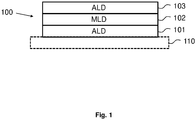
- Fig. 1 shows a strain sensor structure 100 manufactured on a substrate 110.
- the structure comprise a first ALD layer 101 deposited by ALD on the substrate 110, a flexible MLD layer 102 deposited by MLD on the first ALD layer 101, and a second ALD layer 103 deposited by ALD on the MLD layer 102.
- the first and second ALD layers 101, 103 are conductors (such as, ZnO doped with Al 2 O 3 , In 2 O 3 , Ru, Pt and/or their combinations) and the flexible MLD layer 102 is of dielectric material i.e. of electrically insulating material (such as, an alucone film or titanicone or zincone).
- the structure 100 is a capacitor, or an ALD-MLD-ALD capacitor.
- the structure is a capacitor, or an ALD-MLD-ALD capacitor with a (variable) resistance which is or may be affected by mechanical forces or chemical absorption.
- dielectric material is Nb 2 O 5 .
- each of the layers 101-103 and the substrate 110 are biodegradable (but in other embodiments they are not biodegradable, or at least not all of them).
- the flexible MLD layer 102 contracts (is compressed) or expands when it experiences pressure or release of pressure, respectively.
- the capacitance of the capacitor structure changes, which can be detected by a radio frequency signal from outside of the body. For example, an LC circuit or an RLC circuit can be formed which is read from the outside (or reflected power is measured). The change in capacitance will change the response of the circuitry.
- the strain (or compression) experienced by the (coated) substrate for example a bone screw, nail, or stent, is obtained based on the change of the capacitance.
- the said change in capacitance can be induced with various means specific to the capacitor dielectric material(s).
- Fig. 2 shows a schematic perspective view of the sensor structure of Fig. 1 .
- Fig. 2 shows the flexible MLD layer in between two electrically conductive layers (Conductor 1, and Conductor 2).
- the electrically conductive layers have been made by ALD, or by another method. At least part of all said three layers overlap, to form an area where deformation of said flexible layer affects the capacitance measured in between the electrodes (electrically conductive layers).
- the electrically conductive layers may be provided with conductors (conducting wires or other electric pathways) denoted by arrows in Fig. 2 .
- Fig. 3 shows a sensing circuit in accordance with certain embodiments.
- the sensing circuit comprises the capacitor structure (Conductor 1 + MLD layer + Conductor 2) with an attached resistor (attached to Conductor 1) and an antenna (attached to Conductor 2 and to the resistor).
- the antenna may be an inductive element (e.g., an inductor), the circuit then being an RLC circuit.
- the circuit is read from the outside (or reflected power is measured).
- the strain experienced by the (coated) substrate for example a bone screw, nail, or stent, is obtained based on the change of the capacitance.
- the resistor may have been made by ALD.
- Fig. 4 shows another sensor structure in accordance with further embodiments.
- the structure shown in Fig. 4 corresponds to that of Fig. 2 except that one of the electrically conductive layers has a hole (or holes) or opening (or openings) through which molecules or ions can go through and absorb to the MLD layer changing the capacitance of the capacitor or its electrical properties, such as electrical conductivity (in an alternative embodiment, said one of the electrically conductive layers has porosity with a similar effect).
- the structure can be used e.g. as an ion detector.
- An RLC circuit can be formed similarly as in Fig. 3 for example.
- the embodiments provide an MLD layer used as a dielectric layer of a (variable) capacitor or a variable resistor.
- the MLD layer is flexible enabling the capacitor (and/or resistive properties) to be adjustable by strain, such as pressure or compression, induced on it or applied to it.
- the MLD layer is biodegradable. It may be made of MLD materials, such as, but not limited to alucone, titanicone and zincone. The performance and properties of the said MLD layer can be modified with doping with other ALD and MLD layers or ALD pulses.
- the implant is conductive, it implant itself can be work, and be connected as antenna.
- the MLD layer is be coated with conductive materials.
- the conductive materials on both sides of the MLD layer can be made with processes known as such, e.g., Al 2 O 3 +ZnO, conducting biocompatible material. Its resistivity can be adjusted by the ratio of the said materials.
- Thin films are however preferred, in order to have a minimum thickness and impact to the environment where they are used.
- the MLD layer can be coated with an electrically insulating layer having a selected thickness, such as ALD deposited Al 2 O 3 .
- the capacitor can be used as a part of an RC circuit or an RLC circuit known as such in various wireless communication solutions.
- the resistor of the RC or RLC circuit can be made by ALD and with bio decomposable materials.
- the antenna, if any, of the RC or RLC circuitry can be made by ALD and with bio decomposable materials.
- the circuit (or circuitry) is read with external means, such as antenna inducing RF excitation sufficient to cause included current to the RC circuitry, which is dependent on the varying of capacitance C of the capacitor made with MLD which is deforming, such as compressing for thinner thickness under external load. Variation of the circuitry behavior can be further measured with external means to get an indication of the applied force for example.
- the complete assembly can be at least partially coated by a bio-non-dissolving layer, such as a SiO/HfO laminate, made with ALD or similar, or by any such layer bio-dissolving in significantly longer time than the sensor structure.
- a bio-non-dissolving layer such as a SiO/HfO laminate, made with ALD or similar, or by any such layer bio-dissolving in significantly longer time than the sensor structure.
- the capacitance and/or resistance is changed by absorbance of molecules or ions to the MLD layer, which absorption is enabled by surrounding (or adjacent) layer.
- the surrounding layer (which may be made by ALD) may be transmitting detectable materials, or it may be patterned to have holes for the said transmission of material.
- the said transmission may also be ion exchange.
- the said openings can be also further coated with material affecting the transmission of absorbing species.
- an advantage obtained by certain embodiments is that the shape of the used bio implant may not be affected while it can be used in measurement of the force induced to it. Further, in some cases, the bio implant screw for example may be intended to decompose, and it is beneficial that the embedded sensors are also decomposed.
Landscapes
- Health & Medical Sciences (AREA)
- Life Sciences & Earth Sciences (AREA)
- Engineering & Computer Science (AREA)
- Surgery (AREA)
- Physics & Mathematics (AREA)
- General Health & Medical Sciences (AREA)
- Orthopedic Medicine & Surgery (AREA)
- Molecular Biology (AREA)
- Animal Behavior & Ethology (AREA)
- Veterinary Medicine (AREA)
- Public Health (AREA)
- Medical Informatics (AREA)
- Heart & Thoracic Surgery (AREA)
- Biomedical Technology (AREA)
- Chemical & Material Sciences (AREA)
- Pathology (AREA)
- Biophysics (AREA)
- General Physics & Mathematics (AREA)
- Nuclear Medicine, Radiotherapy & Molecular Imaging (AREA)
- Neurology (AREA)
- Computer Networks & Wireless Communication (AREA)
- Chemical Kinetics & Catalysis (AREA)
- Manufacturing & Machinery (AREA)
- Microelectronics & Electronic Packaging (AREA)
- Transplantation (AREA)
- Organic Chemistry (AREA)
- Metallurgy (AREA)
- Power Engineering (AREA)
- Electrochemistry (AREA)
- Analytical Chemistry (AREA)
- Biochemistry (AREA)
- Immunology (AREA)
- Mechanical Engineering (AREA)
- Materials Engineering (AREA)
- General Chemical & Material Sciences (AREA)
- Measurement Of Length, Angles, Or The Like Using Electric Or Magnetic Means (AREA)
- Prostheses (AREA)
Applications Claiming Priority (1)
| Application Number | Priority Date | Filing Date | Title |
|---|---|---|---|
| US201962825968P | 2019-03-29 | 2019-03-29 |
Publications (1)
| Publication Number | Publication Date |
|---|---|
| EP3714772A1 true EP3714772A1 (fr) | 2020-09-30 |
Family
ID=69960568
Family Applications (1)
| Application Number | Title | Priority Date | Filing Date |
|---|---|---|---|
| EP20165498.5A Ceased EP3714772A1 (fr) | 2019-03-29 | 2020-03-25 | Capteur et son procédé de fabrication |
Country Status (4)
| Country | Link |
|---|---|
| US (1) | US11976989B2 (fr) |
| EP (1) | EP3714772A1 (fr) |
| JP (1) | JP7565161B2 (fr) |
| CN (1) | CN111750772A (fr) |
Citations (5)
| Publication number | Priority date | Publication date | Assignee | Title |
|---|---|---|---|---|
| US7754563B2 (en) * | 2006-07-20 | 2010-07-13 | Elpida Memory, Inc. | Nanolaminate-structure dielectric film forming method |
| EP2755023A1 (fr) * | 2013-01-11 | 2014-07-16 | MEAS France | Capteur capacitif intégré dans un circuit semi-conducteur |
| US20160235456A1 (en) * | 2013-10-10 | 2016-08-18 | Dongguan Eontec Co., Ltd. | Biodegradable bone nail |
| US20160304341A1 (en) * | 2014-01-24 | 2016-10-20 | The Regents Of The University Of Colorado, A Body Corporate | Novel Methods of Preparing Nanodevices |
| US20160354174A1 (en) * | 2015-06-05 | 2016-12-08 | Innovative In Vivo Sensing, Llc | Wireless strain sensing device |
Family Cites Families (13)
| Publication number | Priority date | Publication date | Assignee | Title |
|---|---|---|---|---|
| US20030139690A1 (en) | 2000-01-07 | 2003-07-24 | Nikolaus Aebli | Device for in vivo measurement of pressures and pressure variations in or on bones |
| KR100493040B1 (ko) | 2002-12-30 | 2005-06-07 | 삼성전자주식회사 | 반도체 소자의 커패시터 및 그 제조방법 |
| JP2009519114A (ja) | 2005-12-12 | 2009-05-14 | ヴァージニア コモンウェルス ユニバーシティ | 自己感覚性ステント、スマート材料利用のステント、薬剤伝達システム、その他の医療用器具および圧電性材料の医療への利用 |
| TWI353304B (en) * | 2007-10-23 | 2011-12-01 | Sino American Silicon Prod Inc | Transparent conductive component utilized in touch |
| WO2011115643A1 (fr) * | 2010-03-17 | 2011-09-22 | The Board Of Trustees Of The University Of Illinois | Dispositifs biomédicaux implantables sur substrats biorésorbables |
| US9196849B2 (en) | 2013-01-09 | 2015-11-24 | Research & Business Foundation Sungkyunkwan University | Polymer/inorganic multi-layer encapsulation film |
| KR101816967B1 (ko) | 2013-09-30 | 2018-01-09 | 주식회사 엘지화학 | 유기전자소자용 기판 및 이의 제조방법 |
| EP3063791B1 (fr) * | 2013-10-30 | 2018-05-30 | Robert Bosch GmbH | Procédé permettant de former un capteur semi-conducteur à base d'oxyde métallique à l'aide d'un dépôt de couches atomiques et capteur semi-conducteur à base d'oxyde métallique correspondant |
| CN104714672B (zh) * | 2013-12-11 | 2019-04-09 | 昆山工研院新型平板显示技术中心有限公司 | 压敏型显示屏触控单元、触摸屏及其制造方法 |
| WO2015180988A1 (fr) * | 2014-05-28 | 2015-12-03 | Koninklijke Philips N.V. | Procédé de fabrication d'un agencement de piste conductrice flexible, agencement de piste conductrice flexible et système de neurostimulation |
| EP3048185A1 (fr) | 2015-01-20 | 2016-07-27 | BASF Coatings GmbH | Procédé de production de stratifiés organiques-inorganiques flexibles |
| CN105902346B (zh) | 2016-05-25 | 2018-05-15 | 张家港市仁和医疗器械有限公司 | 一种残疾人全地形代步车 |
| WO2018146146A1 (fr) | 2017-02-08 | 2018-08-16 | Trinamix Gmbh | Détecteur pour détection optique d'au moins un objet |
-
2020
- 2020-03-25 EP EP20165498.5A patent/EP3714772A1/fr not_active Ceased
- 2020-03-27 JP JP2020056917A patent/JP7565161B2/ja active Active
- 2020-03-27 US US16/832,161 patent/US11976989B2/en active Active
- 2020-03-27 CN CN202010231126.5A patent/CN111750772A/zh active Pending
Patent Citations (5)
| Publication number | Priority date | Publication date | Assignee | Title |
|---|---|---|---|---|
| US7754563B2 (en) * | 2006-07-20 | 2010-07-13 | Elpida Memory, Inc. | Nanolaminate-structure dielectric film forming method |
| EP2755023A1 (fr) * | 2013-01-11 | 2014-07-16 | MEAS France | Capteur capacitif intégré dans un circuit semi-conducteur |
| US20160235456A1 (en) * | 2013-10-10 | 2016-08-18 | Dongguan Eontec Co., Ltd. | Biodegradable bone nail |
| US20160304341A1 (en) * | 2014-01-24 | 2016-10-20 | The Regents Of The University Of Colorado, A Body Corporate | Novel Methods of Preparing Nanodevices |
| US20160354174A1 (en) * | 2015-06-05 | 2016-12-08 | Innovative In Vivo Sensing, Llc | Wireless strain sensing device |
Non-Patent Citations (4)
| Title |
|---|
| BYOUNG H. LEE ET AL: "Alucone Alloys with Tunable Properties Using Alucone Molecular Layer Deposition and Al 2 O 3 Atomic Layer Deposition", JOURNAL OF PHYSICAL CHEMISTRY C, vol. 116, no. 5, 1 February 2012 (2012-02-01), US, pages 3250 - 3257, XP055693803, ISSN: 1932-7447, DOI: 10.1021/jp209003h * |
| CLEMENTINE M. BOUTRY ET AL: "A stretchable and biodegradable strain and pressure sensor for orthopaedic application", NATURE ELECTRONICS, vol. 1, no. 5, 1 May 2018 (2018-05-01), pages 314 - 321, XP055707410, DOI: 10.1038/s41928-018-0071-7 * |
| PLUM T J ET AL: "Design of a MEMS capacitive chemical sensor based on polymer swelling", MICROELECTRONICS AND ELECTRON DEVICES, 2006. WMED '06. 2006 IEEE WORKS HOP ON BOISE, ID, USA APRIL 14, 2006, PISCATAWAY, NJ, USA,IEEE, 14 April 2006 (2006-04-14), pages 49 - 50, XP010935613, ISBN: 978-1-4244-0374-5, DOI: 10.1109/WMED.2006.1678304 * |
| SUK-WON WANG ET AL: "A Physically Transient Form of Silicon Electronics", SCIENCE, vol. 337, 16 August 2012 (2012-08-16), pages 1640 - 1644, XP055693414, DOI: 10.1126/science.1226325 * |
Also Published As
| Publication number | Publication date |
|---|---|
| US20200309620A1 (en) | 2020-10-01 |
| JP2020165972A (ja) | 2020-10-08 |
| US11976989B2 (en) | 2024-05-07 |
| CN111750772A (zh) | 2020-10-09 |
| JP7565161B2 (ja) | 2024-10-10 |
Similar Documents
| Publication | Publication Date | Title |
|---|---|---|
| US10575780B2 (en) | Measuring of a physiological parameter using a wearable sensor | |
| EP3764872B1 (fr) | Dispositif de surveillance intravasculaire | |
| JP2018532985A (ja) | 電気活性ポリマセンサ及び検知方法 | |
| JPH0319599B2 (fr) | ||
| WO2018013725A1 (fr) | Système et procédé de mesure de paramètres de débit sanguin dans un vaisseau sanguin ayant une prothèse endovasculaire | |
| RU2764122C2 (ru) | Исполнительная структура и ее способ срабатывания | |
| WO2011146122A1 (fr) | Matériaux et procédés d'isolation de composants électroniques et dispositifs associés | |
| WO2021034368A2 (fr) | Détection de contrainte à base de film mince conformable avec substrat flexible | |
| Lipscomb et al. | The effect of relative humidity, temperature and electrical field on leakage currents in piezo-ceramic actuators under dc bias | |
| RU2768159C2 (ru) | Датчик потока и способ измерения скорости потока | |
| US20050096719A1 (en) | Implantable leads permitting functional status monitoring | |
| US11976989B2 (en) | Sensor and its manufacturing method | |
| Rajala et al. | High bending-mode sensitivity of printed piezoelectric poly (vinylidenefluoride-co-trifluoroethylene) sensors | |
| US10429252B1 (en) | Flexible capacitive pressure sensor | |
| US11504506B2 (en) | Strain sensor for a medical devices with improved measurement sensitivity | |
| EP2137741A1 (fr) | Conducteur extensible et son procédé de production | |
| EP3462575A1 (fr) | Dispositif de commande sans fil, système et procédé de commande sans fil | |
| Je et al. | A thin-film piezoelectric PVDF-TrFE based implantable pressure sensor using lithographic patterning | |
| US20220066067A1 (en) | Device for measuring the perceived temperature | |
| US8732922B2 (en) | Parylene-C as a piezoelectric material and method to make it | |
| CN217366207U (zh) | 柔性数字心血管支架 | |
| Sridhar et al. | A hydrogel-based wireless sensor using micromachined variable inductors with folded flex-circuit structures for biomedical applications | |
| US20250213193A1 (en) | Stretchable encapsulation for implantable biomedical devices | |
| JPS62217153A (ja) | 容量式薄膜湿度センサおよびその製造方法 | |
| AGAFONOV et al. | ST. PETERSBURG STATE POLYTECHNICAL UNIVERSITY JOURNAL. PHYSICS AND MATHEMATICS |
Legal Events
| Date | Code | Title | Description |
|---|---|---|---|
| PUAI | Public reference made under article 153(3) epc to a published international application that has entered the european phase |
Free format text: ORIGINAL CODE: 0009012 |
|
| STAA | Information on the status of an ep patent application or granted ep patent |
Free format text: STATUS: THE APPLICATION HAS BEEN PUBLISHED |
|
| AK | Designated contracting states |
Kind code of ref document: A1 Designated state(s): AL AT BE BG CH CY CZ DE DK EE ES FI FR GB GR HR HU IE IS IT LI LT LU LV MC MK MT NL NO PL PT RO RS SE SI SK SM TR |
|
| AX | Request for extension of the european patent |
Extension state: BA ME |
|
| STAA | Information on the status of an ep patent application or granted ep patent |
Free format text: STATUS: REQUEST FOR EXAMINATION WAS MADE |
|
| 17P | Request for examination filed |
Effective date: 20210325 |
|
| RBV | Designated contracting states (corrected) |
Designated state(s): AL AT BE BG CH CY CZ DE DK EE ES FI FR GB GR HR HU IE IS IT LI LT LU LV MC MK MT NL NO PL PT RO RS SE SI SK SM TR |
|
| STAA | Information on the status of an ep patent application or granted ep patent |
Free format text: STATUS: EXAMINATION IS IN PROGRESS |
|
| 17Q | First examination report despatched |
Effective date: 20221006 |
|
| REG | Reference to a national code |
Ref country code: DE Ref legal event code: R079 Free format text: PREVIOUS MAIN CLASS: A61B0005000000 Ipc: G01N0027220000 |
|
| GRAP | Despatch of communication of intention to grant a patent |
Free format text: ORIGINAL CODE: EPIDOSNIGR1 |
|
| STAA | Information on the status of an ep patent application or granted ep patent |
Free format text: STATUS: GRANT OF PATENT IS INTENDED |
|
| RIC1 | Information provided on ipc code assigned before grant |
Ipc: A61B 5/00 20060101ALI20240924BHEP Ipc: A61B 17/72 20060101ALI20240924BHEP Ipc: A61B 17/86 20060101ALI20240924BHEP Ipc: A61B 17/84 20060101ALI20240924BHEP Ipc: H01L 21/02 20060101ALI20240924BHEP Ipc: G01N 27/22 20060101AFI20240924BHEP |
|
| INTG | Intention to grant announced |
Effective date: 20241014 |
|
| GRAJ | Information related to disapproval of communication of intention to grant by the applicant or resumption of examination proceedings by the epo deleted |
Free format text: ORIGINAL CODE: EPIDOSDIGR1 |
|
| STAA | Information on the status of an ep patent application or granted ep patent |
Free format text: STATUS: EXAMINATION IS IN PROGRESS |
|
| INTC | Intention to grant announced (deleted) | ||
| STAA | Information on the status of an ep patent application or granted ep patent |
Free format text: STATUS: THE APPLICATION HAS BEEN REFUSED |
|
| 18R | Application refused |
Effective date: 20251110 |