EP3716312A1 - Dispositif à faisceau de particules chargées pour l'inspection d'un échantillon à l'aide d'une pluralité de mini-faisceaux de particules chargées - Google Patents
Dispositif à faisceau de particules chargées pour l'inspection d'un échantillon à l'aide d'une pluralité de mini-faisceaux de particules chargées Download PDFInfo
- Publication number
- EP3716312A1 EP3716312A1 EP19165969.7A EP19165969A EP3716312A1 EP 3716312 A1 EP3716312 A1 EP 3716312A1 EP 19165969 A EP19165969 A EP 19165969A EP 3716312 A1 EP3716312 A1 EP 3716312A1
- Authority
- EP
- European Patent Office
- Prior art keywords
- charged particle
- specimen
- beam device
- detector
- beamlets
- Prior art date
- Legal status (The legal status is an assumption and is not a legal conclusion. Google has not performed a legal analysis and makes no representation as to the accuracy of the status listed.)
- Pending
Links
- 239000002245 particle Substances 0.000 title claims abstract description 151
- 238000007689 inspection Methods 0.000 title claims abstract description 7
- 230000004907 flux Effects 0.000 claims abstract description 21
- 230000005855 radiation Effects 0.000 claims abstract description 20
- 230000004044 response Effects 0.000 claims abstract description 17
- 238000000034 method Methods 0.000 claims description 13
- 230000008878 coupling Effects 0.000 claims description 8
- 238000010168 coupling process Methods 0.000 claims description 8
- 238000005859 coupling reaction Methods 0.000 claims description 8
- 239000007787 solid Substances 0.000 claims description 5
- 239000000523 sample Substances 0.000 description 34
- 238000010894 electron beam technology Methods 0.000 description 12
- 238000001514 detection method Methods 0.000 description 11
- 238000013461 design Methods 0.000 description 6
- 238000013459 approach Methods 0.000 description 5
- 230000008901 benefit Effects 0.000 description 4
- 230000003287 optical effect Effects 0.000 description 4
- 239000011521 glass Substances 0.000 description 3
- XUIMIQQOPSSXEZ-UHFFFAOYSA-N Silicon Chemical compound [Si] XUIMIQQOPSSXEZ-UHFFFAOYSA-N 0.000 description 2
- 230000004075 alteration Effects 0.000 description 2
- 238000010276 construction Methods 0.000 description 2
- 238000012937 correction Methods 0.000 description 2
- 230000005684 electric field Effects 0.000 description 2
- 238000003384 imaging method Methods 0.000 description 2
- 239000000463 material Substances 0.000 description 2
- 239000000203 mixture Substances 0.000 description 2
- 229910052710 silicon Inorganic materials 0.000 description 2
- 239000010703 silicon Substances 0.000 description 2
- 206010010071 Coma Diseases 0.000 description 1
- 230000000712 assembly Effects 0.000 description 1
- 238000000429 assembly Methods 0.000 description 1
- 230000000903 blocking effect Effects 0.000 description 1
- 230000002708 enhancing effect Effects 0.000 description 1
- 230000002349 favourable effect Effects 0.000 description 1
- 239000011159 matrix material Substances 0.000 description 1
- 238000012986 modification Methods 0.000 description 1
- 230000004048 modification Effects 0.000 description 1
- 230000002093 peripheral effect Effects 0.000 description 1
- 230000000644 propagated effect Effects 0.000 description 1
- 238000000926 separation method Methods 0.000 description 1
- 238000003325 tomography Methods 0.000 description 1
- 239000012780 transparent material Substances 0.000 description 1
Images



Classifications
-
- H—ELECTRICITY
- H01—ELECTRIC ELEMENTS
- H01J—ELECTRIC DISCHARGE TUBES OR DISCHARGE LAMPS
- H01J37/00—Discharge tubes with provision for introducing objects or material to be exposed to the discharge, e.g. for the purpose of examination or processing thereof
- H01J37/02—Details
- H01J37/04—Arrangements of electrodes and associated parts for generating or controlling the discharge, e.g. electron-optical arrangement or ion-optical arrangement
- H01J37/05—Electron or ion-optical arrangements for separating electrons or ions according to their energy or mass
-
- G—PHYSICS
- G01—MEASURING; TESTING
- G01N—INVESTIGATING OR ANALYSING MATERIALS BY DETERMINING THEIR CHEMICAL OR PHYSICAL PROPERTIES
- G01N23/00—Investigating or analysing materials by the use of wave or particle radiation, e.g. X-rays or neutrons, not covered by groups G01N3/00 – G01N17/00, G01N21/00 or G01N22/00
- G01N23/22—Investigating or analysing materials by the use of wave or particle radiation, e.g. X-rays or neutrons, not covered by groups G01N3/00 – G01N17/00, G01N21/00 or G01N22/00 by measuring secondary emission from the material
- G01N23/225—Investigating or analysing materials by the use of wave or particle radiation, e.g. X-rays or neutrons, not covered by groups G01N3/00 – G01N17/00, G01N21/00 or G01N22/00 by measuring secondary emission from the material using electron or ion
- G01N23/2251—Investigating or analysing materials by the use of wave or particle radiation, e.g. X-rays or neutrons, not covered by groups G01N3/00 – G01N17/00, G01N21/00 or G01N22/00 by measuring secondary emission from the material using electron or ion using incident electron beams, e.g. scanning electron microscopy [SEM]
-
- H—ELECTRICITY
- H01—ELECTRIC ELEMENTS
- H01J—ELECTRIC DISCHARGE TUBES OR DISCHARGE LAMPS
- H01J37/00—Discharge tubes with provision for introducing objects or material to be exposed to the discharge, e.g. for the purpose of examination or processing thereof
- H01J37/02—Details
- H01J37/04—Arrangements of electrodes and associated parts for generating or controlling the discharge, e.g. electron-optical arrangement or ion-optical arrangement
- H01J37/147—Arrangements for directing or deflecting the discharge along a desired path
-
- H—ELECTRICITY
- H01—ELECTRIC ELEMENTS
- H01J—ELECTRIC DISCHARGE TUBES OR DISCHARGE LAMPS
- H01J37/00—Discharge tubes with provision for introducing objects or material to be exposed to the discharge, e.g. for the purpose of examination or processing thereof
- H01J37/02—Details
- H01J37/20—Means for supporting or positioning the object or the material; Means for adjusting diaphragms or lenses associated with the support
-
- H—ELECTRICITY
- H01—ELECTRIC ELEMENTS
- H01J—ELECTRIC DISCHARGE TUBES OR DISCHARGE LAMPS
- H01J37/00—Discharge tubes with provision for introducing objects or material to be exposed to the discharge, e.g. for the purpose of examination or processing thereof
- H01J37/02—Details
- H01J37/244—Detectors; Associated components or circuits therefor
-
- H—ELECTRICITY
- H01—ELECTRIC ELEMENTS
- H01J—ELECTRIC DISCHARGE TUBES OR DISCHARGE LAMPS
- H01J37/00—Discharge tubes with provision for introducing objects or material to be exposed to the discharge, e.g. for the purpose of examination or processing thereof
- H01J37/26—Electron or ion microscopes; Electron or ion diffraction tubes
- H01J37/266—Measurement of magnetic or electric fields in the object; Lorentzmicroscopy
- H01J37/268—Measurement of magnetic or electric fields in the object; Lorentzmicroscopy with scanning beams
-
- H—ELECTRICITY
- H01—ELECTRIC ELEMENTS
- H01J—ELECTRIC DISCHARGE TUBES OR DISCHARGE LAMPS
- H01J37/00—Discharge tubes with provision for introducing objects or material to be exposed to the discharge, e.g. for the purpose of examination or processing thereof
- H01J37/26—Electron or ion microscopes; Electron or ion diffraction tubes
- H01J37/28—Electron or ion microscopes; Electron or ion diffraction tubes with scanning beams
-
- H—ELECTRICITY
- H01—ELECTRIC ELEMENTS
- H01J—ELECTRIC DISCHARGE TUBES OR DISCHARGE LAMPS
- H01J2237/00—Discharge tubes exposing object to beam, e.g. for analysis treatment, etching, imaging
- H01J2237/20—Positioning, supporting, modifying or maintaining the physical state of objects being observed or treated
- H01J2237/2007—Holding mechanisms
-
- H—ELECTRICITY
- H01—ELECTRIC ELEMENTS
- H01J—ELECTRIC DISCHARGE TUBES OR DISCHARGE LAMPS
- H01J2237/00—Discharge tubes exposing object to beam, e.g. for analysis treatment, etching, imaging
- H01J2237/244—Detection characterized by the detecting means
- H01J2237/2443—Scintillation detectors
-
- H—ELECTRICITY
- H01—ELECTRIC ELEMENTS
- H01J—ELECTRIC DISCHARGE TUBES OR DISCHARGE LAMPS
- H01J2237/00—Discharge tubes exposing object to beam, e.g. for analysis treatment, etching, imaging
- H01J2237/244—Detection characterized by the detecting means
- H01J2237/2446—Position sensitive detectors
-
- H—ELECTRICITY
- H01—ELECTRIC ELEMENTS
- H01J—ELECTRIC DISCHARGE TUBES OR DISCHARGE LAMPS
- H01J2237/00—Discharge tubes exposing object to beam, e.g. for analysis treatment, etching, imaging
- H01J2237/244—Detection characterized by the detecting means
- H01J2237/24475—Scattered electron detectors
-
- H—ELECTRICITY
- H01—ELECTRIC ELEMENTS
- H01J—ELECTRIC DISCHARGE TUBES OR DISCHARGE LAMPS
- H01J2237/00—Discharge tubes exposing object to beam, e.g. for analysis treatment, etching, imaging
- H01J2237/245—Detection characterised by the variable being measured
- H01J2237/24592—Inspection and quality control of devices
-
- H—ELECTRICITY
- H01—ELECTRIC ELEMENTS
- H01J—ELECTRIC DISCHARGE TUBES OR DISCHARGE LAMPS
- H01J2237/00—Discharge tubes exposing object to beam, e.g. for analysis treatment, etching, imaging
- H01J2237/26—Electron or ion microscopes
- H01J2237/28—Scanning microscopes
- H01J2237/2813—Scanning microscopes characterised by the application
- H01J2237/2817—Pattern inspection
Definitions
- the invention relates to a charged particle beam device for inspection of a specimen with a plurality of charged particle beamlets, the charged particle beam device comprising:
- the illuminator comprises a multi-aperture lens plate having a grid of apertures for defining the corresponding plurality of charged particle beamlets.
- the aperture array typically plays a double role.
- the apertures define the individual beamlets as they are cut out of a single, large beam that is emitted by (for example) a field emitter gun. Hence, they serve as beam limiting apertures for the individual beamlets.
- the individual apertures serve as (micro) lenses for the beamlets.
- (virtual) crossovers are created for the beamlets in a different plane than the common crossovers for the beam as a whole. This allows (for example) to focus the beamlets as probes on a specimen in a regular two-dimensional pattern.
- a different aperture array can be used for the lensing than the one that is used for the beam definition.
- BSEs backscattered electrons
- BSE yield values also give information on the atomic number constitution of the specimen.
- BSEs tend to show preferential energies and/or emission angles as a function of depth, and can therefore serve as a useful basis for performing tomography.
- BSE fluxes (with associated information) precipitated by the various input beams tend to become mixed/jumbled just a short distance above the specimen surface, e.g. of the order of just a few microns for typical beam array configurations (such as 14x14 beams at (specimen-level) orthogonal separations of ca. 3 ⁇ m, for example). Consequently, if a conventional BSE detection architecture is used, it will basically register a convoluted mix of BSEs. Hence, one of the challenges in backscattered electron detection, especially in these multi-beamlet devices, exists in correctly assigning detected backscattered electrons to the corresponding beamlet.
- a charged particle beam device for inspection of a specimen with a plurality of charged particle beamlets.
- the charged particle beam device comprises a specimen holder for holding a specimen, a source for producing a beam of charged particles, and an illuminator for converting said beam of charged particles into a plurality of charged particle beamlets, as well as for focusing said plurality of charged particle beamlets onto said specimen.
- the charged particle beam device comprises a detector assembly for detecting a flux of radiation emanating from the specimen in response to said irradiation by said plurality of charged particle beamlets.
- the charged particle beam device is arranged for directing said plurality of charged particle beamlets onto said specimen in an essentially 1D (one dimensional) pattern.
- Said essentially 1D pattern forms part of an edge of an essentially 2D geometric shape.
- the essentially 1D pattern can be a line, but can also be a spline, a curve, a circle, or combinations thereof.
- the plurality of charged particle beamlet spots are arranged in such a way that they are all positioned on an outer boundary or circumference of an essentially 2D (two-dimensional) geometric shape.
- the geometric shape can be a rectangle, square, triangle, circle, or the like.
- the detector assembly comprises a plurality of detector units positioned in a corresponding essentially 1D pattern, wherein each detector unit is arranged for detecting a flux of radiation emanating from the specimen in response to irradiation by an associated one of said plurality of charged particle beamlets.
- said essentially 1D pattern comprises a straight line.
- Said essentially 1D pattern may additionally, or alternatively comprise a curved line.
- Said essentially 1D pattern may comprise a semi-circle or a (part of a) circle.
- the charged particle beam device is arranged for scanning said sample with said plurality of charged particle beamlets. This allows a larger part of the specimen to be investigated in an effective manner.
- An effective scanning of said sample may be obtained when said charged particle beam device is arranged for reciprocal movement of the plurality of charged particle beamlets in a first direction, as well as for reciprocal movement of the specimen holder in a second direction that is substantially orthogonal to the first direction.
- the specimen may be moved in the second direction, e.g. from left to right, whilst concurrently the beamlets can be moved back and forth, i.e. in a reciprocal manner, in the first direction, e.g. up and down.
- This allows for a large area of the sample to be scanned in a quick and effective manner. It will be clear that alternative movement schemes are conceivable as well.
- the sample may be moved in a reciprocal manner, whilst the beamlets are moved from up to down. It is noted that during movement of the charged particle beamlets in the first direction, and movement of the specimen holder in the second direction, additional movement of the charged particle beamlets in the second direction and/or additional movement of the specimen holder in the first direction is conceivable as well, to allow for drift corrections, distortion corrections and the like.
- said detector assembly is a BSE detector assembly, comprising a plurality of BSE detector units.
- At least one of the plurality of detector units comprises a housing having a front end surface that is directed to a corresponding charged particle beamlet, as well as a bottom surface that is directed to said sample.
- the set-up allows the detector unit to be positioned relatively close to the corresponding charged particle beamlet, which aids in assigning the detected signal to the correct charged particle beamlet.
- said bottom surface comprises a detector element for detecting said flux of radiation emanating from the specimen in response to irradiation by said corresponding charged particle beamlet.
- the detector element may alternatively, or additionally, said front end surface comprises a detector element.
- Said detector element may comprise a scintillation layer and/or a monocrystalline scintillator.
- said detector element comprises a photonic sensor or solid state direct electron sensor.
- said detector unit comprises a lightguide element for direct light coupling of said detector element.
- Said lightguide element may be arranged for direct light coupling of said scintillation layer to said photonic sensor.
- a monocrystalline scintillator that functions as the detector element and the lightguide element.
- the monocrystalline scintillator can be in contact with the photonic sensor or solid state direct electron sensor.
- the lightguide element extends over a distance of at least 5 mm, in particular at least 10 mm.
- the approach of using an essentially 1D pattern allows for direct light coupling from the scintillator to a photonic sensor via a lightguide element.
- a circle or semi circle 1D pattern is used for the plurality of beamlets -and hence for the detector units as well- this allows the lightguide to occupy a constant sector of a circle (constant angle), which allows the lightguide to expand from microns-sized dimensions into millimetres after approximately 10 mm distance from the optical axis.
- This enables the use of discrete photodiodes/photomultipliers for each beamlet channel. With this a higher speed (> 1 MHz) compared to CMOS cameras (up to kHz) can be obtained.
- the discrete sensors such as PMT or SiPM
- the design as presented herein offers better light collection using the lightguide element and significantly easier alignment and robustness and complexity-reduction using a monolithic detection element, without having to resort to complicated and challenging detector assemblies.
- the 1D-pattern (linear or circular) can be advantageously used for simple routing of signal lines from each detection areas, which would not be possible in the tightly packed 2D grid as used in the prior art.
- a method of inspecting a specimen with a plurality of charged particle beamlets comprising the steps of:
- the method comprises the steps of:
- said detecting is in particular done using a plurality of detector units that are arranged in a corresponding essentially 1D pattern.
- the method comprises the step of scanning said sample with said charged particle beamlets, in particular by moving said charged particle beamlets onto said specimen in a first direction and concurrently moving said specimen in a second direction substantially orthogonal to said first direction.
- detecting a flux of radiation comprises the step of detecting backscattered electrons.
- the distance between the detector and the specimen is kept constant during inspecting said specimen. Additionally, the distance between the detector and the beamlets may be kept constant during inspection. Distance may be kept constant by moving the stage. Other ways of achieving this result are conceivable as well.
- a mutual position of the plurality of charged particle beamlets and the corresponding plurality of detector elements is aligned. This way, the center of the detector element and the central position of the beamlet match in tangential direction, and the perpendicular distance of the detector element edge and the beamlet can be kept small and substantially constant during system operation.
- FIG. 1 shows an example of a charged particle beam device, in the form of a Multi-Beam Scanning Electron Microscope (MBSEM).
- the MBSEM 1 comprises a multi beam charged particle generator 2a for generating an array of primary charged particle beams 3, in this case an array of primary electron beams 3.
- the multi beam electron generator 2a comprises at least one electron source 4 for generating a diverging electron beam 5.
- the diverging electron beam 5 is split into an array of focused primary electron beams 3 by an aperture lens array 6.
- the primary electron beams 3 are subsequently directed towards a sample 15, as schematically indicated by the arrow P.
- the sample can be positioned on a stage, so that it can be positioned in a desired manner with respect to the charged particle beamlets 3.
- the multiple images of the source 4 are positioned on the object principle plane of an accelerator lens 7.
- the accelerator lens 7 directs the primary electron beams 3 towards the optical axis 8 and creates a first common cross-over 9 of all the primary electron beams 3.
- the first common cross-over 9 is imaged by the magnetic condenser lens 10 onto a variable aperture 11 that acts as a current limiting aperture. At the variable aperture 11 a second common cross-over of all the primary electron beams 3 is created.
- the MBSEM comprises a lens system 13, 14 for directing the primary charged particle beams from the common cross-over at the variable aperture 11 towards the sample surface 15 and for focusing all primary charged particle beams 3 into an array of individual spots on the sample surface 15.
- the lens system comprises an intermediate magnetic lens 13 for imaging the variable aperture 11 onto a coma free plane of the objective lens 14, which objective lens 14 creates an array of focused primary electron beams on the sample surface 15.
- MBSEM is provided with scan coils 16 for scanning the array of focused primary electron beams over the sample surface 15.
- the MBSEM shown in this embodiment is furthermore provided with a position sensitive secondary electron detector 12 positioned at least substantially in or near a plane comprising a common cross-over, in this case directly below the variable aperture 11.
- This secondary electron detection system 12 is arranged to acquire the individual secondary electron image of each single primary electron beam spot on the sample surface 15. This means, that when the sample surface 15 is scanned in this MBSEM 1, multiple images can be acquired at the same time in one single scan period.
- the charged particle beam device 1 as shown in Fig. 1 is arranged for inspection of a specimen 15 with a plurality of charged particle beamlets 3.
- the charged particle beam device comprises a specimen holder 15 for holding a specimen; a source 4 for producing a beam 5 of charged particles; an illuminator 2b for converting said beam 5 of charged particles into a plurality of charged particle beamlets 3 and directing said plurality of charged particle beamlets 3 onto said specimen 15.
- the illuminator 2b comprises a multi-aperture lens plate 6 having a plurality of apertures for defining the corresponding plurality of charged particle beamlets; as well as at least a first electrode 61 for generating an electrical field at a surface of the multi-aperture lens plate 6; and a detector 12 for detecting a flux of radiation emanating from the specimen 15 in response to said irradiation by said plurality of charged particle beamlets.
- the general setup as shown here in Fig. 1 is known to those skilled in the art, for example from EP 2 864 997 B1 , and modifications to this set up are known to those skilled in the art as well.
- the charged particle device 1 as disclosed herein comprises a multi-aperture lens plate 6, wherein the apertures in said multi-aperture lens plate 6 have a noncircular cross-sectional shape. This will be discussed in more detail with respect to several embodiments as shown in Fig. 2 to Fig. 7 . With the multi-aperture lens plate, imaging resolution is improved.
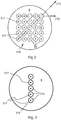
- Figure 2 shows a regular grid 319 of apertures 315 formed in a multi-aperture plate 6 according to the prior art.
- Each non-peripheral aperture, or central aperture, "a” has four directly neighbouring apertures “b", “c", “d” and “e”, and it has four second closest neighbouring apertures, or diagonally neighbouring, "f', "g", "h” and “i”.
- Figure 2 indicates a basic array vector [10] in which apertures 315 are arrayed at the closest neighbour pitch, and Figure 2 indicates a basic array vector [11] in which the apertures 315 are arrayed with a second closest neighbour pitch.
- Each aperture has a center 317.
- the apertures shown here are arranged in a 5 x 5 matrix, having external apertures i, b, f, c, g positioned on a contour or edge of the grid, and internal apertures e, a, h, d positioned within an interior of the grid.
- an aperture plate 6 Using such an aperture plate 6, a convoluted mix of BSEs is detected in case conventional BSE detection architecture is used.
- one of the challenges in backscattered electron detection especially in these multi-beamlet devices, exists in correctly assigning detected backscattered electrons to the corresponding beamlet.
- Fig. 3 shows a setup according to an embodiment of the disclosure.
- the multi-aperture plate 6 comprises plurality of apertures 315 that are arranged to form a line.
- the charged particle beam device is able to direct said plurality of charged particle beamlets onto said specimen in an essentially 1D pattern, in this case in the form of a straight line. Due to this essentially 1D pattern, it is possible to arrange the detector assembly to comprise a plurality of detector units arranged in a corresponding essentially 1D pattern, with each detector unit positioned relatively close to the corresponding beamlet such that the detected signal can be correctly assigned to the corresponding charged particle beamlet.
- the essentially 1D pattern comprises a straight line. It could alternatively be a curved line.
- the essentially 1D pattern is arranged in such a way that the pattern is free from internal apertures.
- internal apertures such as internal apertures e, a, h, d as shown in Fig. 2 , makes it relatively hard to discern a first flux of radiation emanating from the specimen in response to irradiation by a first charged particle beamlet, from a second, neighbouring, flux of radiation emanating from the specimen in response to irradiation by a second, neighbouring, charged particle beamlet.
- the individual detector units To be able to do this, would require the individual detector units to be arranged relatively close to the specimen, and relatively close to the charged particle beamlet as well. Especially for internal apertures this is difficult, as the available room for placing a detector unit is too small.
- the above requirements can be met when the plurality of charged particle beamlets form an essentially 1D pattern, in particular wherein said essentially 1D pattern forms part of an edge of an essentially 2D geometric shape.
- the 2D geometric shape can be a square, rectangle, triangle, circle, or parts thereof. This allows all detector units to approach the sample and the corresponding charged particle beamlet from the side, i.e. from the outer contour of the essentially 2D geometric shape.
- the detector unit can be positioned close enough to the sample, and close enough to the corresponding beamlet, to ensure that the detected signal is emanating from the corresponding charged particle beamlet.
- said detector assembly is a Back Scatter Electron (BSE) detector assembly, comprising a plurality of BSE detector units.
- the plurality of detectors may be arranged in a corresponding 1D pattern as well, or may be arranged in a different 1D pattern.
- the detector units are arranged in an alternating fashion, e.g. alternating on both (left and right) sides of the charged particle beamlets. This results in a zig-zag 1D pattern for the detector units.
- two dedicated detector elements each from a different side to collect signal generated by the very same beamlet and thus enhancing the signal collection efficiency and improving the image SNR.
- a further embodiment of a multi-aperture plate allowing the charged particle beam device as disclosed herein to direct said plurality of charged particle beamlets onto said specimen in an essentially 1D pattern.
- the multi-aperture plate comprises two rows 319a, 319b of apertures 315, that are positioned side by side.
- the essentially 1D pattern forms part of an edge of a square or rectangle 325 (dotted line).
- the detector units in a corresponding essentially 1D pattern, to allow reliable detection of a flux of radiation emanating from the specimen in response to irradiation by an associated one of said plurality of charged particle beamlets.
- detectors associated with the first row 319a can be positioned on the left hand side of the drawing
- detectors associated with the second row 319b can be positioned on the right hand side of the drawing.
- a multi-aperture plate 6 for defining the essentially 1D pattern of charged particle beamlets. It will be understood by those skilled in the art, that other ways of achieving this essentially 1D pattern are possible as well. Further, in Fig. 3 , a total of five apertures are used, and in Fig. 4 a total of ten apertures are used. it is conceivable however that any number of apertures are used in the essentially 1D pattern.
- the desired 1D pattern is obtained by blocking a number of apertures in a multi-aperture plate 6.
- the beamlets coming from internal apertures e.g. e, a, h, d
- the beamlets reaching the sample are able to form an essentially 1D pattern, defined by the outer contour of an essentially 2D geometric shape (in this case, a square), which allows detector units to be positioned in a corresponding 1D pattern as well.
- a further embodiment of a multi-aperture plate is shown, allowing the particle beam device as disclosed herein to direct said plurality of charged particle beamlets onto said specimen in an essentially 1D pattern.
- the essentially 1D pattern comprises two sub-parts of a circle 325.
- the arrangement is quite similar to the two row linear arrangement of Fig. 4 , although two main differences exist: first, the two rows 319a, 319b used in Fig. 5 are arranged on circle 325, i.e. they are positioned on the outer contour or outline of the 2D geometric shape (which, in this case, is a circle 325). Second, the second row 319b has a slight offset with respect to the first row 319a.
- FIG. 5 shows a coordinate axis x,y to illustrate this.
- the second row 319b is slightly offset in (minus) y-direction compared to the first row 319a.
- the offset is such that a given aperture of the first row 319a is in between adjacent apertures of the second row 319b.
- This strategy is applicable to the embodiment of Fig. 4 as well.
- This off-set or staggering arrangement has several advantages in effectively and efficiently scanning the sample, as will be discussed next with respect to Fig. 6 . It is noted that in a single row, adjacent apertures preferably have the same distance in y-direction, although the distance in x-direction may vary in this case as the apertures are essentially placed on the outer contour of circle 325.
- FIG. 6 a schematic top view of the charged particle beamlet arrangement described herein is shown. It is shown a schematic top view of the sample 15, comprising a plurality of sample regions S a -S k . It is noted here that not all sample regions are provided with a reference numeral, for clarity purposes. Each sample region S a -S k has an associated charged particle beamlet 3a-3k.
- the sample 15 can be moved in the positive (and negative) x-direction (indicated by arrow S s ).
- the charged particle beamlets can be moved in positive and negative y-direction. Additional movements of the sample and the beamlets is conceivable as well.
- the charged particle beam device is arranged for scanning said sample with said plurality of charged particle beamlets.
- the scanning path S a -S k of a single beamlet is indicated in Fig. 6 .
- the placement of the beams in a 1D pattern in the form of the outline of a circle ensures that detector units can be placed near to the respective beamlets (see Fig. 7 ), but also ensures that aberrations are minimized.
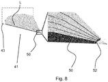
- FIG. 7 the positioning of the detector units 41a-41e with respect to the charged particle beamlets 3a-3e is shown in het left hand part of the figure, and a cross-sectional view of a single detector unit 41 is shown in the right hand part of the figure. It can be seen that the charged particle beamlets 3a-3e are positioned in the form of part of a circle. It is noted that the left part of the Fig. 7 only shows a part of the setup, and the complete setup could be similar to the setup shown in Fig. 6 . However, it is also conceivable that the setup as shown in one or more of Fig. 3-5 is used.
- the individual detector units 41 can be positioned relatively close to the sample 15, as well as close to the corresponding charged particle beamlet 3a-3e.
- the detector units 41a-41e can approach the corresponding charged particle beamlet from an outer part of the outer contour of the essentially 2D geometric shape (which, in the embodiment shown is a circle).
- the essentially 2D geometric shape can be a square, rectangle, triangle, semi-circle, circle, or any other shape, or parts or combinations thereof. Due to the detectors being able to approach the outer contour of the 2D geometric shape defined by the particle beamlets 3a-3e, there is sufficient space available to embody the detector units. In other words, the 1D pattern defined by the charged particle beamlets relieves the space constraints for the corresponding detector units.
- FIG. 7 The cross-section of Fig. 7 shows a single charged particle beamlet 3 impinging on the surface of the sample 15, thereby generating a flux of radiation R.
- a detector unit 41 is positioned close to the surface of the sample, and close to the charged particle beamlet 3.
- the detector unit 41 comprises a housing 50, with a front end surface 52 that is directed to the corresponding charged particle beamlet 3, as well as a bottom surface 51 that is directed to said sample.
- the housing comprises a top surface 53 as well.
- the front end surface 52 connects the bottom surface 51 to the top surface 53.
- a further circumferential wall (not shown) can be provided as well.
- the bottom surface 51 comprises a detector element 42 for detecting said flux of radiation R emanating from the specimen 15 in response to irradiation by said corresponding charged particle beamlet 3.
- the front end surface 52 may be provided with such a detector element 42.
- the detector element can be a relatively thin layer of scintillation material.
- the detector 41 comprises a light guide L formed inside the housing 50 and arranged for direct light coupling of said detector element.
- the light guide can either be an empty space inside a polished reflective "housing", or a glass part where the light is propagated through the glass and reflected from the light-vacuum boundary by total reflection.
- light is coupled from the sensor surface 42 to a Photonic sensor 43.
- the sensor surface 42 can be a thin scintillator layer.
- the sensor 42 can be a solid state direct electron sensor.
- the housing 50 can be made from transparent material e.g. glass and act as lightguide L and detector element 42 can be a thin layer of scintillation material placed on the light-guide surface and a photonic sensor 43 coupled to it.
- the housing 50 with detector element 42 can be a monocrystalline scintillator with functionality of sensor surface 42, which also acts as the light guide L for coupling to the photonic sensor 43.
- the housing 50 carries a solid state direct electron sensor 42.
- sensor element 43 can be absent.
- a setup of the detector assembly with a total of five individual detector units 41 is shown.
- the beamlets are arranged on the outer contour of a circle as 2D geometric shape, having a diameter of approximately 100 ⁇ m.
- the lightguide L connects the front end of the detector unit to an array of individual sensors 43 (schematically indicated here by dashed line).
- the length of the lightguide L shown here is approximately 10 mm, and the end face near the sensor 43 is approximately 2mm wide, enabling good detector-sensor coupling.
- the 1D pattern (linear, square or circular) can be leveraged for simple routing of signal lines from each detection area. This would not be possible in the tightly packed 2D array of charged particle beamlets that is used in the prior art.
Landscapes
- Chemical & Material Sciences (AREA)
- Analytical Chemistry (AREA)
- Physics & Mathematics (AREA)
- Health & Medical Sciences (AREA)
- Life Sciences & Earth Sciences (AREA)
- Biochemistry (AREA)
- General Health & Medical Sciences (AREA)
- General Physics & Mathematics (AREA)
- Immunology (AREA)
- Pathology (AREA)
- Analysing Materials By The Use Of Radiation (AREA)
Priority Applications (4)
| Application Number | Priority Date | Filing Date | Title |
|---|---|---|---|
| EP19165969.7A EP3716312A1 (fr) | 2019-03-28 | 2019-03-28 | Dispositif à faisceau de particules chargées pour l'inspection d'un échantillon à l'aide d'une pluralité de mini-faisceaux de particules chargées |
| US16/825,827 US20200312610A1 (en) | 2019-03-28 | 2020-03-20 | Charged particle beam device for inspection of a specimen with a plurality of charged particle beamlets |
| JP2020055227A JP7499049B2 (ja) | 2019-03-28 | 2020-03-26 | 複数の荷電粒子ビームレットで試料を検査するための荷電粒子ビーム装置 |
| CN202010230636.0A CN111755302A (zh) | 2019-03-28 | 2020-03-27 | 用于通过多个带电粒子分束来检查样品的带电粒子束装置 |
Applications Claiming Priority (1)
| Application Number | Priority Date | Filing Date | Title |
|---|---|---|---|
| EP19165969.7A EP3716312A1 (fr) | 2019-03-28 | 2019-03-28 | Dispositif à faisceau de particules chargées pour l'inspection d'un échantillon à l'aide d'une pluralité de mini-faisceaux de particules chargées |
Publications (1)
| Publication Number | Publication Date |
|---|---|
| EP3716312A1 true EP3716312A1 (fr) | 2020-09-30 |
Family
ID=66001076
Family Applications (1)
| Application Number | Title | Priority Date | Filing Date |
|---|---|---|---|
| EP19165969.7A Pending EP3716312A1 (fr) | 2019-03-28 | 2019-03-28 | Dispositif à faisceau de particules chargées pour l'inspection d'un échantillon à l'aide d'une pluralité de mini-faisceaux de particules chargées |
Country Status (4)
| Country | Link |
|---|---|
| US (1) | US20200312610A1 (fr) |
| EP (1) | EP3716312A1 (fr) |
| JP (1) | JP7499049B2 (fr) |
| CN (1) | CN111755302A (fr) |
Families Citing this family (3)
| Publication number | Priority date | Publication date | Assignee | Title |
|---|---|---|---|---|
| EP3882951A1 (fr) * | 2020-03-19 | 2021-09-22 | FEI Company | Dispositif à faisceau de particules chargées pour l'inspection d'un échantillon à l'aide d'une pluralité de faisceaux de particules chargées |
| JP7571443B2 (ja) | 2020-10-01 | 2024-10-23 | 株式会社オートネットワーク技術研究所 | 検出回路及び給電制御装置 |
| CN119758429A (zh) * | 2024-01-30 | 2025-04-04 | 中国科学院高能物理研究所 | 二次电子探测器、扫描电子束成像装置、方法 |
Citations (6)
| Publication number | Priority date | Publication date | Assignee | Title |
|---|---|---|---|---|
| US4954705A (en) * | 1989-01-25 | 1990-09-04 | Siemens Aktiengesellschaft | Method for examining a specimen in a particle beam instrument |
| US20040135515A1 (en) * | 2001-05-01 | 2004-07-15 | Muneki Hamashima | Electron beam apparatus and device manufacturing method using same |
| US20060145087A1 (en) * | 2004-09-10 | 2006-07-06 | Parker N W | Apparatus and method for inspection and testing of flat panel display substrates |
| US20060169899A1 (en) * | 2004-09-10 | 2006-08-03 | Parker N W | Detector optics for multiple electron beam test system |
| EP2864997A1 (fr) | 2012-06-22 | 2015-04-29 | Technische Universiteit Delft | Appareil et procédé permettant d'inspecter la surface d'un échantillon |
| US20180254167A1 (en) * | 2017-03-01 | 2018-09-06 | Dongfang Jingyuan Electron Limited | Patterned Substrate Imaging Using Multiple Electron Beams |
Family Cites Families (13)
| Publication number | Priority date | Publication date | Assignee | Title |
|---|---|---|---|---|
| TWI297167B (en) * | 2000-06-27 | 2008-05-21 | Ebara Corp | Inspection apparatus and inspection method |
| JP2002353279A (ja) * | 2001-05-25 | 2002-12-06 | Hitachi Ltd | 回路パターン検査方法とその装置 |
| EP1619495A1 (fr) * | 2004-07-23 | 2006-01-25 | Nederlandse Organisatie voor toegepast-natuurwetenschappelijk Onderzoek TNO | Méthode et appareil pour inspecter une surface d'un échantillon et utilisation des matériaux fluorescents |
| EP2365514B1 (fr) * | 2010-03-10 | 2015-08-26 | ICT Integrated Circuit Testing Gesellschaft für Halbleiterprüftechnik mbH | Colonne de particules chargées de faisceau double et son procédé de contrôle |
| US8362425B2 (en) * | 2011-03-23 | 2013-01-29 | Kla-Tencor Corporation | Multiple-beam system for high-speed electron-beam inspection |
| NL2009696C2 (en) * | 2012-10-25 | 2014-04-29 | Univ Delft Tech | Apparatus and method for inspecting a surface of a sample. |
| US9190241B2 (en) * | 2013-03-25 | 2015-11-17 | Hermes-Microvision, Inc. | Charged particle beam apparatus |
| EP2924708A1 (fr) * | 2014-03-25 | 2015-09-30 | Fei Company | Imagerie d'un échantillon à l'aide de faisceaux multiples et de détecteurs multiples |
| EP3010031B1 (fr) * | 2014-10-16 | 2017-03-22 | Fei Company | Microscope à particules chargées avec plaque d'ouverture spéciale |
| US10366862B2 (en) * | 2015-09-21 | 2019-07-30 | KLA-Tencor Corporaton | Method and system for noise mitigation in a multi-beam scanning electron microscopy system |
| JP6750966B2 (ja) * | 2016-06-01 | 2020-09-02 | 株式会社ニューフレアテクノロジー | パターン検査装置及びパターン検査方法 |
| JP2018181407A (ja) * | 2017-04-03 | 2018-11-15 | 株式会社ニューフレアテクノロジー | マルチ荷電粒子ビーム検査装置及びマルチ荷電粒子ビーム検査方法 |
| US10249472B2 (en) * | 2017-07-13 | 2019-04-02 | ICT Integrated Circuit Testing Gesellschaft für Halbleiterprüftechnik mbH | Charged particle beam device, charged particle beam influencing device, and method of operating a charged particle beam device |
-
2019
- 2019-03-28 EP EP19165969.7A patent/EP3716312A1/fr active Pending
-
2020
- 2020-03-20 US US16/825,827 patent/US20200312610A1/en not_active Abandoned
- 2020-03-26 JP JP2020055227A patent/JP7499049B2/ja active Active
- 2020-03-27 CN CN202010230636.0A patent/CN111755302A/zh active Pending
Patent Citations (6)
| Publication number | Priority date | Publication date | Assignee | Title |
|---|---|---|---|---|
| US4954705A (en) * | 1989-01-25 | 1990-09-04 | Siemens Aktiengesellschaft | Method for examining a specimen in a particle beam instrument |
| US20040135515A1 (en) * | 2001-05-01 | 2004-07-15 | Muneki Hamashima | Electron beam apparatus and device manufacturing method using same |
| US20060145087A1 (en) * | 2004-09-10 | 2006-07-06 | Parker N W | Apparatus and method for inspection and testing of flat panel display substrates |
| US20060169899A1 (en) * | 2004-09-10 | 2006-08-03 | Parker N W | Detector optics for multiple electron beam test system |
| EP2864997A1 (fr) | 2012-06-22 | 2015-04-29 | Technische Universiteit Delft | Appareil et procédé permettant d'inspecter la surface d'un échantillon |
| US20180254167A1 (en) * | 2017-03-01 | 2018-09-06 | Dongfang Jingyuan Electron Limited | Patterned Substrate Imaging Using Multiple Electron Beams |
Non-Patent Citations (1)
| Title |
|---|
| ROBINSON V N E: "IMAGING WITH BACKSCATTERED ELECTRONS IN A SCANNING ELECTRON MICROSCOPE", SCANNING, JOHN WILEY & SONS, INC, US, vol. 3, 28 July 1979 (1979-07-28), pages 15 - 26, XP000847630, ISSN: 0161-0457 * |
Also Published As
| Publication number | Publication date |
|---|---|
| US20200312610A1 (en) | 2020-10-01 |
| JP7499049B2 (ja) | 2024-06-13 |
| CN111755302A (zh) | 2020-10-09 |
| JP2020167159A (ja) | 2020-10-08 |
Similar Documents
| Publication | Publication Date | Title |
|---|---|---|
| KR102557713B1 (ko) | 다중-빔 입자 빔 현미경 작동 방법 | |
| CN104903710B (zh) | 检测样品表面的装置和方法 | |
| US7732762B2 (en) | Method of inspecting a specimen surface, apparatus and use of fluorescent material | |
| KR102179897B1 (ko) | 시료를 검사하기 위한 방법 및 하전 입자 다중-빔 디바이스 | |
| JP3723260B2 (ja) | 粒子ビーム・コラム | |
| US7084406B2 (en) | Detector arrangement and detection method | |
| US20150069235A1 (en) | Particle Optical System | |
| US20200312610A1 (en) | Charged particle beam device for inspection of a specimen with a plurality of charged particle beamlets | |
| US10937627B2 (en) | Multi-beam electron microscope | |
| EP2654069A1 (fr) | Détecteur à multiples canaux, éléments optiques associés et son procédé de fonctionnement | |
| TWI523064B (zh) | 可切換式多視角偵測器與用於其之光學器件及其操作方法 | |
| US9984848B2 (en) | Multi-beam lens device, charged particle beam device, and method of operating a multi-beam lens device | |
| EP1389795B1 (fr) | Système de microscopie électronique et méthode d'utilisation | |
| US20240128051A1 (en) | Multi-beam charged particle beam system with anisotropic filtering for improved image contrast | |
| JP2025520499A (ja) | マルチビーム粒子顕微鏡を動作させる方法、コンピュータプログラム製品、およびマルチビーム粒子顕微鏡 | |
| JP2024535055A (ja) | デフォーカスされるビームの誘導でコントラスト動作モードにおいてマルチビーム粒子顕微鏡を動作させるための方法、コンピュータプログラムおよびマルチビーム粒子顕微鏡 | |
| JP2026501033A (ja) | 検出器アレイを用いるマルチビーム電子顕微鏡検査のためのシステム及び方法 | |
| EP1883094B1 (fr) | Appareil à faisceau de particules et procédé pour l'examen d'un échantillon | |
| CN110709960B (zh) | 带电粒子束装置 | |
| WO2025202056A1 (fr) | Système à faisceaux d'électrons multiples pour inspection avec des électrons rétrodiffusés | |
| JP2025084114A (ja) | サンプルを画像化するための方法及びシステム | |
| KR20260042597A (ko) | 하전 입자 검출 시스템 | |
| JP2002141015A (ja) | 基体検査装置及び方法 |
Legal Events
| Date | Code | Title | Description |
|---|---|---|---|
| PUAI | Public reference made under article 153(3) epc to a published international application that has entered the european phase |
Free format text: ORIGINAL CODE: 0009012 |
|
| STAA | Information on the status of an ep patent application or granted ep patent |
Free format text: STATUS: THE APPLICATION HAS BEEN PUBLISHED |
|
| AK | Designated contracting states |
Kind code of ref document: A1 Designated state(s): AL AT BE BG CH CY CZ DE DK EE ES FI FR GB GR HR HU IE IS IT LI LT LU LV MC MK MT NL NO PL PT RO RS SE SI SK SM TR |
|
| AX | Request for extension of the european patent |
Extension state: BA ME |
|
| STAA | Information on the status of an ep patent application or granted ep patent |
Free format text: STATUS: REQUEST FOR EXAMINATION WAS MADE |
|
| 17P | Request for examination filed |
Effective date: 20210224 |
|
| RBV | Designated contracting states (corrected) |
Designated state(s): AL AT BE BG CH CY CZ DE DK EE ES FI FR GB GR HR HU IE IS IT LI LT LU LV MC MK MT NL NO PL PT RO RS SE SI SK SM TR |
|
| STAA | Information on the status of an ep patent application or granted ep patent |
Free format text: STATUS: EXAMINATION IS IN PROGRESS |
|
| 17Q | First examination report despatched |
Effective date: 20240116 |