EP3716396A1 - Antenne und kommunikationsvorrichtung - Google Patents
Antenne und kommunikationsvorrichtung Download PDFInfo
- Publication number
- EP3716396A1 EP3716396A1 EP18891956.7A EP18891956A EP3716396A1 EP 3716396 A1 EP3716396 A1 EP 3716396A1 EP 18891956 A EP18891956 A EP 18891956A EP 3716396 A1 EP3716396 A1 EP 3716396A1
- Authority
- EP
- European Patent Office
- Prior art keywords
- impedance
- antenna
- radio frequency
- variable
- frequency front
- Prior art date
- Legal status (The legal status is an assumption and is not a legal conclusion. Google has not performed a legal analysis and makes no representation as to the accuracy of the status listed.)
- Pending
Links
- 238000004891 communication Methods 0.000 title claims abstract description 29
- 239000003990 capacitor Substances 0.000 claims description 30
- 230000008859 change Effects 0.000 claims description 22
- 238000013459 approach Methods 0.000 claims description 7
- 230000002452 interceptive effect Effects 0.000 abstract description 10
- 230000005855 radiation Effects 0.000 abstract description 10
- 238000010586 diagram Methods 0.000 description 24
- 238000000034 method Methods 0.000 description 20
- 230000005540 biological transmission Effects 0.000 description 17
- 230000008569 process Effects 0.000 description 12
- 238000012360 testing method Methods 0.000 description 10
- 238000013461 design Methods 0.000 description 9
- 230000007246 mechanism Effects 0.000 description 8
- 230000008878 coupling Effects 0.000 description 6
- 238000010168 coupling process Methods 0.000 description 6
- 238000005859 coupling reaction Methods 0.000 description 6
- 238000012795 verification Methods 0.000 description 4
- 238000006243 chemical reaction Methods 0.000 description 3
- 238000004590 computer program Methods 0.000 description 3
- 230000000694 effects Effects 0.000 description 3
- 230000011664 signaling Effects 0.000 description 3
- 238000004458 analytical method Methods 0.000 description 2
- 238000004364 calculation method Methods 0.000 description 2
- 230000007423 decrease Effects 0.000 description 2
- 238000003780 insertion Methods 0.000 description 2
- 230000037431 insertion Effects 0.000 description 2
- 239000000463 material Substances 0.000 description 2
- 230000005405 multipole Effects 0.000 description 2
- 238000012545 processing Methods 0.000 description 2
- 230000033228 biological regulation Effects 0.000 description 1
- 230000021615 conjugation Effects 0.000 description 1
- 238000013500 data storage Methods 0.000 description 1
- 238000005516 engineering process Methods 0.000 description 1
- 238000005259 measurement Methods 0.000 description 1
- 230000003287 optical effect Effects 0.000 description 1
- 239000013307 optical fiber Substances 0.000 description 1
- 239000004065 semiconductor Substances 0.000 description 1
- 230000008054 signal transmission Effects 0.000 description 1
- 239000007787 solid Substances 0.000 description 1
- 230000001131 transforming effect Effects 0.000 description 1
- 238000011144 upstream manufacturing Methods 0.000 description 1
Images




Classifications
-
- H—ELECTRICITY
- H01—ELECTRIC ELEMENTS
- H01Q—ANTENNAS, i.e. RADIO AERIALS
- H01Q5/00—Arrangements for simultaneous operation of antennas on two or more different wavebands, e.g. dual-band or multi-band arrangements
- H01Q5/30—Arrangements for providing operation on different wavebands
- H01Q5/307—Individual or coupled radiating elements, each element being fed in an unspecified way
- H01Q5/314—Individual or coupled radiating elements, each element being fed in an unspecified way using frequency dependent circuits or components, e.g. trap circuits or capacitors
- H01Q5/335—Individual or coupled radiating elements, each element being fed in an unspecified way using frequency dependent circuits or components, e.g. trap circuits or capacitors at the feed, e.g. for impedance matching
-
- H—ELECTRICITY
- H01—ELECTRIC ELEMENTS
- H01Q—ANTENNAS, i.e. RADIO AERIALS
- H01Q5/00—Arrangements for simultaneous operation of antennas on two or more different wavebands, e.g. dual-band or multi-band arrangements
- H01Q5/50—Feeding or matching arrangements for broad-band or multi-band operation
-
- H—ELECTRICITY
- H01—ELECTRIC ELEMENTS
- H01Q—ANTENNAS, i.e. RADIO AERIALS
- H01Q1/00—Details of, or arrangements associated with, antennas
- H01Q1/12—Supports; Mounting means
- H01Q1/22—Supports; Mounting means by structural association with other equipment or articles
-
- H—ELECTRICITY
- H01—ELECTRIC ELEMENTS
- H01Q—ANTENNAS, i.e. RADIO AERIALS
- H01Q1/00—Details of, or arrangements associated with, antennas
- H01Q1/52—Means for reducing coupling between antennas; Means for reducing coupling between an antenna and another structure
-
- H—ELECTRICITY
- H01—ELECTRIC ELEMENTS
- H01Q—ANTENNAS, i.e. RADIO AERIALS
- H01Q23/00—Antennas with active circuits or circuit elements integrated within them or attached to them
-
- H—ELECTRICITY
- H01—ELECTRIC ELEMENTS
- H01Q—ANTENNAS, i.e. RADIO AERIALS
- H01Q5/00—Arrangements for simultaneous operation of antennas on two or more different wavebands, e.g. dual-band or multi-band arrangements
- H01Q5/30—Arrangements for providing operation on different wavebands
- H01Q5/307—Individual or coupled radiating elements, each element being fed in an unspecified way
- H01Q5/314—Individual or coupled radiating elements, each element being fed in an unspecified way using frequency dependent circuits or components, e.g. trap circuits or capacitors
- H01Q5/328—Individual or coupled radiating elements, each element being fed in an unspecified way using frequency dependent circuits or components, e.g. trap circuits or capacitors between a radiating element and ground
-
- H—ELECTRICITY
- H01—ELECTRIC ELEMENTS
- H01Q—ANTENNAS, i.e. RADIO AERIALS
- H01Q9/00—Electrically-short antennas having dimensions not more than twice the operating wavelength and consisting of conductive active radiating elements
- H01Q9/04—Resonant antennas
- H01Q9/30—Resonant antennas with feed to end of elongated active element, e.g. unipole
- H01Q9/42—Resonant antennas with feed to end of elongated active element, e.g. unipole with folded element, the folded parts being spaced apart a small fraction of the operating wavelength
-
- H—ELECTRICITY
- H04—ELECTRIC COMMUNICATION TECHNIQUE
- H04B—TRANSMISSION
- H04B1/00—Details of transmission systems, not covered by a single one of groups H04B3/00 - H04B13/00; Details of transmission systems not characterised by the medium used for transmission
- H04B1/02—Transmitters
- H04B1/04—Circuits
- H04B1/0458—Arrangements for matching and coupling between power amplifier and antenna or between amplifying stages
-
- H—ELECTRICITY
- H04—ELECTRIC COMMUNICATION TECHNIQUE
- H04B—TRANSMISSION
- H04B1/00—Details of transmission systems, not covered by a single one of groups H04B3/00 - H04B13/00; Details of transmission systems not characterised by the medium used for transmission
- H04B1/02—Transmitters
- H04B1/04—Circuits
- H04B1/0483—Transmitters with multiple parallel paths
-
- H—ELECTRICITY
- H01—ELECTRIC ELEMENTS
- H01Q—ANTENNAS, i.e. RADIO AERIALS
- H01Q9/00—Electrically-short antennas having dimensions not more than twice the operating wavelength and consisting of conductive active radiating elements
- H01Q9/04—Resonant antennas
- H01Q9/0407—Substantially flat resonant element parallel to ground plane, e.g. patch antenna
- H01Q9/0421—Substantially flat resonant element parallel to ground plane, e.g. patch antenna with a shorting wall or a shorting pin at one end of the element
Definitions
- This application relates to the field of radio frequency microwave technologies, and in particular, to an antenna and a communications apparatus.
- Impedance matching is mainly used for a transmission line to enable load impedance to be equal to characteristic impedance of the transmission line during energy transmission, so that all high frequency microwave signals can only be transmitted to a load point, no signal is reflected back to a source point, and there is no energy loss during signal transmission. It can be learned that the impedance matching can improve energy efficiency.
- the impedance matching is implemented by adjusting an impedance value of a normalized load point and a characteristic impedance value of the transmission line based on a Smith chart (Smith chart). However, in a high frequency circuit, if characteristic impedance of a transmission line does not match load impedance, reflection occurs at a load end.
- radio indicators of impedance of the antenna are optimized. If verification on optimized radio indicators fails, comparatively good antenna matching is selected for circuit commissioning and then active impedance distribution of an output port of an amplifier to an antenna side is tested based on the Smith chart. It is determined whether a TX end of a duplexer needs to be converged.
- an Ant port of the duplexer is commissioned to match an RF end; or if the TX end of the duplexer does not need to be converged, impedance output from a power amplifier (English full name: power amplify, PA for short) is commissioned based on load pull of the radio frequency front end, and then verification is performed on conduction performance of the radio frequency front end and the radio indicators. If the verification succeeds, a commissioning procedure ends.
- a power amplifier English full name: power amplify, PA for short
- an indicator on the radio frequency front end is debugged based on an antenna with impedance of 50 ⁇ .
- impedance of the antenna is restricted by a spacial dimension, actual impedance of the antenna deviates from 50 ohms greatly.
- impedance mismatching occurs between the radio frequency front end and the antenna, a standing wave is formed. Consequently, transmission efficiency of a transmission line is greatly reduced. This is specifically reflected as impedance divergence on a Smith chart.
- an impedance characteristic of the transmission line needs to be manually adjusted on a transmission link, to ensure that all transmission indicators of the transmission link meet a product design requirement.
- This application provides an antenna and a communications apparatus, to resolve a prior-art problem that an impedance matching adjustment mechanism has comparatively low efficiency.
- a first aspect of this application provides an antenna, including:
- variable impedance circuit is configured to: when impedance of the antenna does not match impedance of the radio frequency front end, or when impedance of the radio frequency front end changes, adaptively adjust the impedance of the antenna, to control the impedance of the antenna to match the impedance of the radio frequency front end in a conjugate manner.
- the current antenna needs to transmit an electromagnetic wave signal; if the impedance of the current antenna mismatches the impedance of the radio frequency front end, the at least one variable impedance circuit on the antenna can be adaptively adjusted, for example, the at least one variable impedance circuit may be disposed in at least one of the radiating area, the grounding area, and the feeding area, to adjust the impedance of the antenna to match the impedance of the radio frequency front end in a conjugate manner.
- a specific quantity and locations of variable impedance circuits that need to be adjusted are not limited in this application.
- variable impedance circuit may be configured to: when impedance of the antenna matches impedance of the radio frequency front end, adaptively adjust the impedance of the antenna, to control the impedance of the antenna to mismatch the impedance of the radio frequency front end. For example, when the antenna receives an electromagnetic wave signal from space, the antenna needs to convert the received electromagnetic wave signal into a high frequency electronic signal.
- the at least one variable impedance circuit on the antenna can be adaptively adjusted in the conversion process, for example, the at least one variable impedance circuit may be disposed in the at least one of the radiating area, the grounding area, and the feeding area, to adjust the impedance of the antenna to mismatch the impedance of a radio frequency front end.
- the impedance of the antenna is adjusted to mismatch the impedance of the radio frequency front end, an energy loss of energy of the interfering signal in a radio frequency link can be increased (that is, a link insertion loss at an interfering frequency at which the antenna is located is increased), and therefore interference in a communications apparatus can be reduced.
- a specific quantity and locations of variable impedance circuits that need to be adjusted are not limited in this application.
- variable impedance circuit may include a variable impedance element.
- variable impedance element includes at least a variable capacitor element, a variable resistor element, or a variable inductor element, or the variable impedance element includes at least a circuit obtained by combining at least one of a variable capacitor element, a variable resistor element, or a variable inductor element.
- variable impedance element is configured to: when the impedance of the antenna does not match the impedance of the radio frequency front end, or when the impedance of the radio frequency front end changes, adaptively adjust a value of the variable impedance element, to control the impedance of the antenna to match the impedance of the radio frequency front end in a conjugate manner.
- a tunable element on the radio frequency front end needs to be adjusted based on a particular radiation frequency, to implement that the impedance of the radio frequency front end approaches 50 ⁇ .
- this can be applied to only a frequency band in a particular range, and can be limited to only fixed characteristic impedance (for example, given standard impedance of 50 ⁇ ). Consequently, scalability is comparatively low.
- the variable impedance circuit needs to be added between the radio frequency front end and the antenna, to implement impedance matching between the radio frequency front end and the antenna.
- a circuit board needs to be changed, an integrated level of the circuit board is reduced, and it is also inconvenient to expand the circuit board.
- variable impedance circuit is introduced into the grounding area, the feeding area, or the radiating area of the antenna.
- impedance of the radio frequency front end does not match the impedance of the antenna, there is no need to adjust a tunable element on the radio frequency front end, and there is no need to add a variable impedance circuit between the radio frequency front end and the antenna.
- the variable impedance circuit on the antenna in this application adaptively adjusts the impedance of the antenna, so that conjugate matching is implemented between the impedance of the radio frequency front end and the impedance of the antenna. An energy loss in a radio frequency link is reduced, and overall radiation efficiency of a communications apparatus is improved.
- variable impedance element on the antenna in this application adaptively adjusts the value of the variable impedance element, so that the impedance of the antenna is correspondingly adjusted, and conjugate matching is implemented between the impedance of the radio frequency front end and the impedance of the antenna.
- the antenna in this application can adapt to radio frequency signals in all frequency band ranges, and the impedance of the antenna does not need to be adjusted to fixed 50 ⁇ .
- the antenna in this application can adapt to any value of the impedance of the radio frequency front end. Compared with an original radio frequency tuner (tuner) with a tunable design, the antenna in this application is free from a standard impedance constraint of 50 ⁇ . Therefore, the antenna in this application is easier to be adjusted, has large expansion space, and is easy to be implemented in engineering application.
- variable impedance element adaptively adjusts the value of the variable impedance element, to control automatic adjustment of a coefficient of the impedance of the antenna, to approach or be adjusted to a current coefficient of the impedance of the radio frequency front end, so that the impedance of the antenna matches the antenna at the radio frequency signal. Therefore, a reflection coefficient of the antenna approaches 0, and transmission efficiency is improved.
- variable impedance circuit further includes at least one switching device, the switching device is disposed in a target area, at least one variable impedance element is disposed in the target area, and the target area is at least one of the radiating area, the grounding area, and the feeding area; and the disposed switching device is configured to connect or disconnect the variable impedance element, and is configured to switch the variable impedance element connected to the target area; or the disposed switching device is configured to change at least one attribute in voltage, temperature, humidity, and light intensity of the variable impedance element connected to the switching device, to change the variable impedance element connected to the target area.
- the antenna is configured to: receive an instruction from a processor of the communications apparatus, and switch statuses of switching devices to update a connectivity combination of the switching devices; or the antenna is configured to: receive an instruction from a processor of the communications apparatus, and change at least one attribute in voltage, temperature, humidity, and light intensity of the variable impedance element connected to the switching device, to change the variable impedance element connected to the target area.
- the switching device may include a single-pole multi-throw switch, a multi-pole multi-throw switch, a transistor, a controller, or the like.
- Each switching device may be disconnected or connected by receiving a control signal from a CPU in the radio frequency link, to present a plurality of switching device combinations, and hardware is adaptively adjusted, to control the impedance of the antenna. Specifically, all switching device combinations may be traversed to select an optimal switching device combination, to implement an optimal conjugate matching effect.
- variable impedance element disposed on the antenna is a detachable element.
- a second aspect of this application provides a communications apparatus, including a radio frequency front end and the antenna according to the first aspect.
- modules or submodules described as separate components may be or may not be physically separated, or may be or may not be physical modules, or may not be distributed into a plurality of circuit modules. Objectives of the solutions of this application may be achieved by selecting some or all of the modules based on an actual requirement.
- This application provides an antenna and a communications apparatus, applied to a radio frequency, an antenna, a radar, a millimeter wave, a mobile phone radio frequency, a radio frequency integrated circuit (English full name: radio frequency integrated circuit, RFIC for short), a power amplifier, software-defined radio (English full name: software defined radio, SDR for short), and the like. Detailed descriptions are provided below.
- this application mainly provides the following technical solutions.
- a variable impedance element is introduced into an antenna.
- a variable inductor, a variable capacitor, or a variable resistor is separately disposed in a grounding area, a feeding area, or a radiating area.
- variable impedance element on the antenna in this application adaptively adjusts a value of the variable impedance element, so that the impedance of the antenna is correspondingly adjusted, and conjugate matching is implemented between the impedance of the radio frequency front end and the impedance of the antenna.
- the antenna in this embodiment of this application may be referred to as conjugate antenna.
- the energy output device A may be considered as the radio frequency front end in this embodiment of this application, and the energy input device B may be considered as the antenna that receives a radio frequency signal.
- Characteristic impedance represents such a characteristic or a feature of a specific transmission line, and is a value of instantaneous impedance received by a signal when the signal is transmitted along the transmission line.
- a Smith chart is a calculation chart with equivalent circles for normalized input impedance (or admittance) plotted on a reflection coefficient plane.
- the Smith chart is a graph used for electrical and electronic engineering, and is mainly used for impedance matching on the transmission line.
- the chart includes three circles, used to solve a problem with the transmission line and some waveguide problems by using a graphical method, so as to avoid a complex operation.
- the antenna may include: a radiating area, a grounding area, and a feeding area, where one end of the radiating area is electrically connected to a radio frequency front end, and the radio frequency front end is configured to receive and send an electromagnetic wave signal.
- At least one variable impedance circuit is disposed in at least one of the radiating area, the grounding area, and the feeding area.
- Impedance adjustment in this embodiment of this application is mainly applied to the following two scenarios.
- Scenario 1 When the antenna receives an electromagnetic wave signal from the radio frequency front end, the antenna and the radio frequency front end are in an impedance mismatching status.
- variable impedance circuit is configured to: when impedance of the antenna does not match impedance of the radio frequency front end, or when impedance of the radio frequency front end changes, adaptively adjust the impedance of the antenna, to control the impedance of the antenna to match the impedance of the radio frequency front end in a conjugate manner.
- the variable impedance circuit may include a controller, a variable impedance element, various switching devices, and the like. A specific structure may be obtained by transforming a structure shown in FIG. 1 . This is not specifically limited in this application.
- the current antenna needs to transmit an electromagnetic wave signal; if the impedance of the current antenna mismatches the impedance of the radio frequency front end, the at least one variable impedance circuit on the antenna can be adaptively adjusted, for example, the at least one variable impedance circuit may be disposed in at least one of the radiating area, the grounding area, and the feeding area, to adjust the impedance of the antenna to match the impedance of the radio frequency front end in a conjugate manner.
- a specific quantity and locations of variable impedance circuits that need to be adjusted are not limited in this application.
- Scenario 2 When the antenna receives an electromagnetic wave signal from space, the antenna and the radio frequency front end are in an impedance matching status.
- the variable impedance circuit may be configured to: when the impedance of the antenna matches the impedance of the radio frequency front end, adaptively adjust the impedance of the antenna, to control the impedance of the antenna to mismatch the impedance of the radio frequency front end.
- the antenna when the antenna receives the electromagnetic wave signal from the space, the antenna needs to convert the received electromagnetic wave signal into the high frequency electronic signal. If the antenna system detects that the electromagnetic wave signal is the interfering signal, the at least one variable impedance circuit on the antenna can be adaptively adjusted in the conversion process, for example, the at least one variable impedance circuit may be disposed in at least one of the radiating area, the grounding area, and the feeding area, to adjust the impedance of the antenna to mismatch the impedance of the radio frequency front end.
- an energy loss of energy of the interfering signal in a radio frequency link can be increased (that is, a link insertion loss at an interfering frequency at which the antenna is located is increased), and therefore interference in the communications apparatus can be reduced.
- a specific quantity and locations of variable impedance circuits that need to be adjusted are not limited in this application.
- variable impedance circuit may include the variable impedance element, that is, at least one variable impedance element is disposed in at least one of the radiating area, the grounding area, and the feeding area, or the variable impedance element includes at least a circuit obtained by combining at least one of a variable capacitor element, a variable resistor element, or a variable inductor element.
- variable impedance element may be configured to: when the impedance of the antenna does not match the impedance of the radio frequency front end, or when impedance of the radio frequency front end changes, adaptively adjust a value of the variable impedance element, to control the impedance of the antenna to match the impedance of the radio frequency front end.
- variable impedance element may be configured to: when the impedance of the antenna matches the impedance of the radio frequency front end, adaptively adjust a value of the variable impedance element, to control the impedance of the antenna to mismatch the impedance of radio frequency front end.
- a tunable element on the radio frequency front end needs to be adjusted based on a particular radiation frequency, to implement that the impedance of the radio frequency front end approaches 50 ⁇ .
- this can be applied to only a frequency band in a particular range, and can be limited to only fixed characteristic impedance (for example, given standard impedance of 50 ⁇ ). Consequently, scalability is comparatively low.
- the variable impedance circuit needs to be added between the radio frequency front end and the antenna, to implement impedance matching between the radio frequency front end and the antenna.
- a circuit board needs to be changed, an integrated level of the circuit board is reduced, and it is also inconvenient to expand the circuit board.
- variable impedance circuit is introduced into the grounding area, the feeding area, or the radiating area of the antenna.
- the impedance of the radio frequency front end does not match the impedance of the antenna (namely, Scenario 1)
- there is no need to adjust a tunable element on the radio frequency front end and there is no need to add a variable impedance circuit between the radio frequency front end and the antenna.
- the variable impedance circuit on the antenna in this application adaptively adjusts the impedance of the antenna, so that conjugate matching is implemented between the impedance of the radio frequency front end and the impedance of the antenna. An energy loss in a radio frequency link is reduced, and overall radiation efficiency of the communications apparatus is improved.
- a case in Scenario 2 is similar, and details are not described again.
- variable impedance element on the antenna in this application adaptively adjusts the value of the variable impedance element, so that the impedance of the antenna is correspondingly adjusted, and conjugate matching is implemented between the impedance of the radio frequency front end and the impedance of the antenna.
- the antenna in this application can adapt to radio frequency signals in all frequency band ranges, and the impedance of the antenna does not need to be adjusted to fixed 50 ⁇ .
- the antenna in this application can adapt to any value of the impedance of the radio frequency front end. Compared with an original radio frequency tuner (tuner) with a tunable design, the antenna in this application is free from a standard impedance constraint of 50 ⁇ . Therefore, the antenna in this application is easier to be adjusted, has large expansion space, and is easy to be implemented engineering application.
- the antenna needs to adaptively adjust only the impedance of the antenna, to match the radio frequency front end in a conjugate manner, without considering a plurality of statuses presented for a standard impedance characteristic at different operating frequencies according to an industry regulation. Even if the antenna has the standard impedance characteristic, the antenna is unrelated to the standard impedance characteristic of the antenna in a conjugate matching process.
- the variable impedance element includes at least a variable capacitor element C, a variable resistor element R, a variable inductor element L, or an RC, RL, or RCL combination circuit derived from C, R, and L.
- a variable capacitor element, a variable resistor element, or a variable inductor element may be disposed in each of the radiating area, the grounding area, and the feeding area, or a variable capacitor element, a variable resistor element, or a variable inductor element may be disposed in at least one of the radiating area, the grounding area, and the feeding area.
- variable impedance element disposed in the radiating area, the grounding area, or the feeding area is not limited in this application, a quantity of variable impedance elements disposed in the radiating area, the grounding area, or the feeding area is not limited, and a connection relationship between variable impedance elements disposed in the radiating area, the grounding area, or the feeding area is not limited.
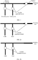
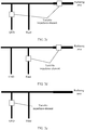
- variable impedance element with a specific type or a value range is disposed in the radiating area, the grounding GND area, or the feeding Feed area, and may be flexibly disposed based on a radio frequency signal. This is not specifically limited in this application. The following separately describes six antenna structures shown in FIG. 2a to FIG. 2g .
- a variable impedance element is disposed in each of a radiating area, GND, and Feed.
- a variable impedance element is disposed in each of a radiating area and GND.
- a variable impedance element is disposed in each of a radiating area and Feed.
- a variable impedance element is disposed in GND.
- a variable impedance element is disposed in Feed.
- a variable impedance element is disposed in a radiating area.
- Another impedance element may be disposed, or no impedance element is disposed in an area in which no variable impedance element is disposed on the antenna (for example, the radiating area, the GND, or the Feed). This is not specifically limited in this application.
- a value range of each variable impedance element disposed in the radiating area, the grounding area, or the feeding area may be further limited.
- a variable impedance element with a corresponding value range may be disposed based on a fixed frequency band, and a plurality of fixed jump points are set, so that a proper fixed point is quickly obtained through traverse.
- variable impedance element disposed in the radiating area, the grounding area, and the feeding area is a detachable element. Due to a detachable characteristic of the variable impedance element, when a frequency of the radio frequency signal changes or the impedance of the radio frequency front end changes, there is no need to change a design of a circuit board, but only a new variable impedance element is used for replacement, or a new antenna is used for replacement, to implement conjugate matching. Compared with the existing mechanism, scalability is comparatively high, and labor costs are reduced.
- the antenna when the impedance of the radio frequency front end is comparatively high, and the installed antenna cannot adapt to the impedance of the radio frequency front end, the antenna may be replaced with an antenna that adapts to the impedance of the current radio frequency front end, or the variable impedance element that is already disposed on the antenna may be replaced, added, removed, or the like. This is not specifically limited in this application.
- An antenna whose frequency band ranges from 700 MHz to 1300 GHz is used as an example.
- the impedance of the radio frequency front end is 50 ⁇
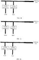
- a variable capacitor C1 and a variable inductor L1 are respectively disposed in a feeding area and a grounding area of an antenna shown in FIG. 3a .
- the antenna shown in FIG. 3a can adapt to radio frequency impedance ranging from 50 ⁇ to 100 ⁇ . If the impedance of the current radio frequency front end is 200 ⁇ , the variable impedance elements on the current antenna need to be replaced.
- variable capacitor C1 in the feeding area in FIG. 3a may be replaced with a variable capacitor C2
- variable inductor L1 in the grounding area may be replaced with a variable inductor L2, as shown in FIG. 3b .
- variable capacitor C1 in the feeding area in FIG. 3a may be replaced with a variable inductor L3
- variable inductor L1 in the grounding area may be replaced with a variable resistor R, as shown in FIG. 3c .
- variable capacitor C1 in the feeding area in FIG. 3a may be replaced with a variable capacitor C3
- variable inductor L1 in the grounding area may be replaced with a variable capacitor C4, as shown in FIG. 3d .
- Variable ranges of L1 and L2 are different, and may have an inclusion relationship or an intersection relationship.
- Variable ranges of C1, C2, C3, and C4 are different, and may have an inclusion relationship or an intersection relationship. This may be specifically set based on an operating frequency band of the antenna, and is not limited in this application.
- the impedance of the antenna may be further dynamically adjusted in this application, to adapt to the impedance output from the radio frequency front end adaptively.
- at least one switching device may be disposed on the antenna, and the switching device is disposed in a target area. At least one variable impedance element is disposed in the target area, and the target area is at least one of the radiating area, the grounding area, and the feeding area.
- the disposed switching device is configured to connect or disconnect the variable impedance element, and is configured to switch the variable impedance element connected to the target area.
- the disposed switching device is configured to change at least one attribute in voltage, temperature, humidity, and light intensity of the variable impedance element connected to the switching device, to change the variable impedance element connected to the target area.
- the switching device may include a single-pole multi-throw switch, a multi-pole multi-throw switch, a transistor, a controller, or the like.
- Each switching device may be disconnected or connected by receiving a control signal from a central processing unit CPU in the radio frequency link, to present a plurality of switching device combinations, and hardware is adaptively adjusted, to control the impedance of the antenna. Specifically, all switching device combinations may be traversed to select an optimal switching device combination, to implement an optimal conjugate matching effect.
- the antenna is configured to: receive an instruction from a processor of the communications apparatus, and switch statuses of switching devices to update a connectivity combination of the switching devices; or the antenna is configured to: receive an instruction from a processor of the communications apparatus, and change at least one attribute in voltage, temperature, humidity, and light intensity of the variable impedance element connected to the switching device, to change the variable impedance element connected to the target area.
- the switching device may be controlled by the CPU in the radio frequency link.
- the CPU may adaptively adjust various preset statuses of corresponding variable impedance elements by using an FET-swith SPDT switch that is in the radio frequency link and that is connected to a reserved GPIO interface of the CPU, for example, may drive some switching devices by using voltage, to obtain a switching device combination.
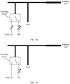
- a switching device for example, a single-pole double-throw switch
- two variable impedance elements that is, a variable capacitor and a variable resistor
- a tester may be connected to the radio frequency link, to test impedance characteristics, mapped to a Smith chart, of the radio frequency front end and the antenna.
- connectivity of the variable impedance elements is adjusted by using software based on the Smith chart, or a value of a connected variable impedance element may be manually adjusted without using the radio frequency link. In this way, the impedance of the antenna may be correspondingly adjusted based on the Smith chart, until conjugate matching is implemented.
- a switching device and a variable resistor are disposed at a GND end. If impedance mismatching occurs currently, a tester may be connected to the radio frequency link, to test impedance characteristics, mapped to a Smith chart, of the radio frequency front end and the antenna. Then, the variable resistor is adjusted by using software based on the Smith chart, or a value of the variable resistor may be manually adjusted without using the radio frequency link. In this way, the impedance of the antenna may be correspondingly adjusted based on the Smith chart, until conjugate matching is implemented.
- variable impedance element When the impedance of the radio frequency front end decreases, a variable impedance element may be introduced into the grounding area. In this way, the impedance of the antenna can decrease, so as to implement conjugate matching.
- a variable impedance element When the impedance of the radio frequency front end increases, a variable impedance element may be introduced into the feeding area. In this way, the impedance of the antenna can increase, so as to implement conjugate matching.
- the antenna introduced in this embodiment of this application has a biggest difference: A parameter S of the radio frequency front end does not need to be tuned to a corresponding frequency by using a tuner, and an energy returning sensor may be added of the radio frequency front end.
- the antenna needs to be adaptively adjusted based on a return loss value collected by the energy returning sensor and a change of the return loss value.
- the antenna in this embodiment of this application does not need to be in a standard impedance mode, and is not associated with parameters (such as S11, a standing wave ratio, and standard impedance) related to antenna performance and load pull of the radio frequency front end, so that the antenna can be adaptively adjusted to be in conjugation with the radio frequency front end.
- variable inductor when a variable inductor is added to the radiating area, it may be equivalent to: ⁇ is lengthened and C remains unchanged. The frequency f correspondingly becomes lower, and a frequency corresponding to a return loss continuously offsets towards a low frequency.
- a variable capacitor when a variable capacitor is added to the radiating area, it may be equivalent to: the radiation arm is broken so that the length of the radiation arm is shortened. The frequency f correspondingly becomes higher, and a frequency corresponding to a return loss (return loss) continuously offsets towards a high frequency.
- FIG. 7 For a schematic diagram of comparison between a TRP and a parameter S11 when the variable inductor and the variable capacitor are disposed in the radiating area and a TRP and a parameter S11 when the variable inductor and the variable capacitor are not added, refer to FIG. 7 .
- the conjugate antenna in this embodiment of this application can operate at any frequency, and can also match the radio frequency front end based on any impedance in a conjugate manner.
- the circuit board does not need to be reconstructed, but only the conjugate antenna needs to be replaced or updated.
- the variable capacitor or the variable inductor is disposed in the grounding area.
- FIG. 5k For a schematic diagram of impedance changes of the antenna at different frequency bands, refer to FIG. 5k .
- a proper variable capacitor or variable inductor may be selected based on the schematic diagram of the impedance changes shown in FIG. 5k .
- FIG. 8 An impedance characteristic of the Wi-Fi antenna is shown in FIG. 8 .
- an S11 change characteristic is measured in two observation modes (Log mag and Smith), and effects in the two observation modes are the same.
- S11 is an input reflection coefficient, namely, an input return loss.
- a test instrument is connected to an output end of an FEM, that is, connected to the output end of the FEM, to test active load pull.
- the test instrument is connected to the output end of the FEM, and the test instrument is used to reversely check the impedance characteristic of the radio frequency front end.
- the impedance characteristic of the radio frequency front end is displayed by using a Smith chart shown in FIG. 9 by using the test instrument.
- FIG. 9 shows two test results in a passive mode of a circuit board and in an electrical signaling mode of the circuit board. When it ranges from 5.1 GHz to 5.7 GHz, an impedance characteristic of the Wi-Fi antenna ranges from 78 ⁇ + j1.11 nH to 119 ⁇ + j916 fF. It can be learned that an actual impedance characteristic of the Wi-Fi antenna is not 50 ⁇ .
- an impedance characteristic of the radio frequency front end is Ra + jXa
- the impedance characteristic of the Wi-Fi antenna is Rb + jXa. Because b corresponding to the Wi-Fi antenna is a fixed value, b cannot vary with a corresponding to the radio frequency front end. Consequently, mismatching between the radio frequency front end and the Wi-Fi antenna is caused.
- the impedance characteristic of the conjugate antenna is Rc + jXc.
- TRP of the low channel CH36 18.7877
- TRP of the medium channel CH100 18.8225
- TRP of the high channel CH140 19.0129
- TRP radio performance in the low channel and the middle channel is improved by 5 dB compared with that of an existing Wi-Fi antenna with standard impedance. It can be learned that the conjugate antenna is introduced and conjugate matching can be implemented because the impedance characteristic of the conjugate antenna varies with an impedance characteristic of an upstream device (namely, the radio frequency front end) corresponding to the conjugate antenna, and therefore an energy loss in a link in an electromagnetic conversion process can be reduced.
- an upstream device namely, the radio frequency front end
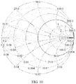
- a Smith curve of a Wi-Fi antenna with standard impedance, a Smith curve of a radio frequency front end, and a Smith curve of conjugate antenna is compared. It can be learned from FIG. 11 that, before the conjugate antenna is introduced, the Smith curve of the Wi-Fi antenna with the standard impedance and the Smith curve of the radio frequency front end present a mismatching status, and after the conjugate antenna is introduced, the Smith curve of the conjugate antenna and the Smith curve of the radio frequency front end present conjugate matching.
- An embodiment of this application further provides a communications apparatus.
- the communications apparatus may include a radio frequency front end and the antenna described in the embodiment corresponding to any one of FIG. 1 to FIG. 11 .
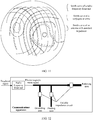
- the communications apparatus may be configured to process interference from an electromagnetic wave in space, or may be configured to process a radiation efficiency problem inside the communications apparatus.
- scenario 1 shown in FIG. 12 and scenario 2 shown in FIG. 13 For details, refer to scenario 1 shown in FIG. 12 and scenario 2 shown in FIG. 13 .
- the disclosed system, apparatus, and method may be implemented in other manners.
- the described apparatus embodiment is merely an example.
- division into the modules is merely logical function division.
- a plurality of modules or components may be combined or integrated into another system, or some features may be ignored or not performed.
- the displayed or discussed mutual couplings or direct couplings or communication connections may be implemented through some interfaces.
- the indirect couplings or communication connections between the apparatuses or modules may be implemented in electronic, mechanical, or other forms.
- modules described as separate parts may or may not be physically separate, and parts displayed as modules may be or may not be physical modules, may be located in one position, or may be distributed on a plurality of network modules. Some or all of the modules may be selected based on an actual requirement to achieve the objectives of the solutions of the embodiments.
- modules in the embodiments of this application may be integrated into one processing module, or each of the modules may exist alone physically, or two or more modules are integrated into one module.
- the integrated module may be implemented in a form of hardware, or may be implemented in a form of a software function module.
- the integrated module may be stored in a computer readable storage medium.
- All or some of the foregoing embodiments may be implemented by software, hardware, firmware, or any combination thereof.
- software is used to implement the embodiments, all or some of the embodiments may be implemented in a form of a computer program product.
- the computer program product includes one or more computer instructions. When the computer program instructions are loaded and executed on a computer, some or all of the procedures or functions according to the embodiments of this application are generated.
- the computer may be a general-purpose computer, a dedicated computer, a computer network, or another programmable apparatus.
- the computer instructions may be stored in a computer-readable storage medium or may be transmitted from a computer-readable storage medium to another computer-readable storage medium.
- the computer instructions may be transmitted from a website, computer, server, or data center to another website, computer, server, or data center in a wired (for example, a coaxial cable, an optical fiber, or a digital subscriber line (DSL)) or wireless (for example, infrared, radio, or microwave) manner.
- a wired for example, a coaxial cable, an optical fiber, or a digital subscriber line (DSL)
- wireless for example, infrared, radio, or microwave
- the computer-readable storage medium may be any usable medium accessible by the computer, or a data storage device, such as a server or a data center, integrating one or more usable media.
- the usable medium may be a magnetic medium (for example, a floppy disk, a hard disk, or a magnetic tape), an optical medium (for example, a DVD), a semiconductor medium (for example, a solid-state drive (Solid State Disk, SSD)), or the like.
Landscapes
- Engineering & Computer Science (AREA)
- Computer Networks & Wireless Communication (AREA)
- Signal Processing (AREA)
- Details Of Aerials (AREA)
- Transceivers (AREA)
Applications Claiming Priority (2)
| Application Number | Priority Date | Filing Date | Title |
|---|---|---|---|
| CN201711404750.5A CN109962329A (zh) | 2017-12-22 | 2017-12-22 | 一种天线及通信装置 |
| PCT/CN2018/119257 WO2019120077A1 (zh) | 2017-12-22 | 2018-12-05 | 一种天线及通信装置 |
Publications (2)
| Publication Number | Publication Date |
|---|---|
| EP3716396A1 true EP3716396A1 (de) | 2020-09-30 |
| EP3716396A4 EP3716396A4 (de) | 2020-12-09 |
Family
ID=66994375
Family Applications (1)
| Application Number | Title | Priority Date | Filing Date |
|---|---|---|---|
| EP18891956.7A Pending EP3716396A4 (de) | 2017-12-22 | 2018-12-05 | Antenne und kommunikationsvorrichtung |
Country Status (4)
| Country | Link |
|---|---|
| US (1) | US20200321699A1 (de) |
| EP (1) | EP3716396A4 (de) |
| CN (1) | CN109962329A (de) |
| WO (1) | WO2019120077A1 (de) |
Families Citing this family (10)
| Publication number | Priority date | Publication date | Assignee | Title |
|---|---|---|---|---|
| KR102632180B1 (ko) * | 2019-08-30 | 2024-02-01 | 삼성전자 주식회사 | 안테나 및 그것을 포함하는 전자 장치 |
| CN111082833B (zh) * | 2019-12-27 | 2021-09-17 | 宇龙计算机通信科技(深圳)有限公司 | 射频前端电路和终端 |
| KR102863007B1 (ko) * | 2020-05-11 | 2025-09-22 | 엘지전자 주식회사 | 전파 방사 장치 및 이를 구비하는 오븐 |
| CN115175455B (zh) * | 2021-04-06 | 2024-11-22 | 英业达科技有限公司 | 平坦化电源递送网路的阻抗的方法 |
| CN115498399B (zh) * | 2021-06-18 | 2025-07-11 | Oppo广东移动通信有限公司 | 天线组件、电子设备和可穿戴设备 |
| CN113992215A (zh) * | 2021-10-22 | 2022-01-28 | 闻泰通讯股份有限公司 | 射频前端发射模块及其带外杂散自适应调节方法 |
| CN114330739A (zh) * | 2021-12-02 | 2022-04-12 | 武汉光目科技有限公司 | 一种基于强化学习的阻抗匹配自动控制方法及系统 |
| CN115986374A (zh) * | 2023-02-22 | 2023-04-18 | 立讯精密工业(昆山)有限公司 | 车载天线装置及其天线模块 |
| CN118738837B (zh) * | 2023-03-31 | 2026-01-13 | 华为技术有限公司 | 一种天线结构和电子设备 |
| US20260005726A1 (en) * | 2024-06-28 | 2026-01-01 | Zebra Technologies Corporaton | Systems and Methods for Dynamic Antenna Tuning of an RFID-Integrated Indicia-Reading Device |
Family Cites Families (16)
| Publication number | Priority date | Publication date | Assignee | Title |
|---|---|---|---|---|
| JP2004096341A (ja) * | 2002-08-30 | 2004-03-25 | Fujitsu Ltd | 共振周波数が可変な逆f型アンテナを含むアンテナ装置 |
| JP4469632B2 (ja) * | 2004-02-24 | 2010-05-26 | 富士通株式会社 | アンテナ整合回路用制御装置 |
| WO2012158693A1 (en) * | 2011-05-16 | 2012-11-22 | Paratek Microwave, Inc. | Method and apparatus for tuning a communication device |
| CN103187626A (zh) * | 2013-03-08 | 2013-07-03 | 华南理工大学 | 一种陷波特性可重构的超宽带平面单极子天线 |
| WO2014165320A2 (en) * | 2013-04-01 | 2014-10-09 | Ethertronics, Inc. | Reconfigurable multi-mode active antenna system |
| KR102229382B1 (ko) * | 2013-08-23 | 2021-03-22 | 삼성전자주식회사 | 전자 장치 및 그를 동작하는 방법 |
| CN104681984B (zh) * | 2013-11-29 | 2019-05-21 | 深圳富泰宏精密工业有限公司 | 无线通信装置 |
| TWI531115B (zh) * | 2013-12-04 | 2016-04-21 | 宏碁股份有限公司 | 通訊裝置 |
| US20160294042A1 (en) * | 2013-12-31 | 2016-10-06 | Huawei Device Co., Ltd. | Loop-shaped antenna and mobile terminal |
| CN104752833A (zh) * | 2013-12-31 | 2015-07-01 | 深圳富泰宏精密工业有限公司 | 天线组件及具有该天线组件的无线通信装置 |
| US9912066B2 (en) * | 2015-07-02 | 2018-03-06 | Mediatek Inc. | Tunable antenna module using frequency-division circuit for mobile device with metal cover |
| WO2017022370A1 (ja) * | 2015-07-31 | 2017-02-09 | 株式会社村田製作所 | アンテナ整合回路、アンテナ回路、フロントエンド回路および通信装置 |
| CN106921034B (zh) * | 2015-12-26 | 2019-03-08 | 小米科技有限责任公司 | 天线组件及电子设备 |
| US9780774B2 (en) * | 2015-12-29 | 2017-10-03 | Infineon Technologies Ag | System and method for a switchable capacitance |
| CN206313756U (zh) * | 2016-12-21 | 2017-07-07 | 珠海全志科技股份有限公司 | 一种可变阻抗调谐装置及带有该装置的射频系统 |
| CN206293622U (zh) * | 2016-12-31 | 2017-06-30 | 惠州硕贝德无线科技股份有限公司 | 一种带阻抗匹配电路的天线 |
-
2017
- 2017-12-22 CN CN201711404750.5A patent/CN109962329A/zh active Pending
-
2018
- 2018-12-05 EP EP18891956.7A patent/EP3716396A4/de active Pending
- 2018-12-05 WO PCT/CN2018/119257 patent/WO2019120077A1/zh not_active Ceased
-
2020
- 2020-06-19 US US16/906,071 patent/US20200321699A1/en not_active Abandoned
Also Published As
| Publication number | Publication date |
|---|---|
| US20200321699A1 (en) | 2020-10-08 |
| WO2019120077A1 (zh) | 2019-06-27 |
| CN109962329A (zh) | 2019-07-02 |
| EP3716396A4 (de) | 2020-12-09 |
Similar Documents
| Publication | Publication Date | Title |
|---|---|---|
| EP3716396A1 (de) | Antenne und kommunikationsvorrichtung | |
| US7075386B2 (en) | Antenna switching circuit | |
| US9214718B2 (en) | Methods for characterizing tunable radio-frequency elements | |
| JP5668029B2 (ja) | 無線回路、周波数ペア決定方法 | |
| EP2424119A1 (de) | Antennenmodul und Impedanzabgleichsverfahren dafür | |
| US20140273887A1 (en) | Tunable ila and dila matching for simultaneous high and low band operation | |
| KR20170093208A (ko) | 조정 가능한 rf 커플러 | |
| EP2851997A1 (de) | Leiterplattenantenne und leiterplatte | |
| JP5435309B2 (ja) | 方向性結合器および無線通信装置 | |
| CN104852148A (zh) | 一种可调谐天线及终端 | |
| CN107395247A (zh) | 一种终端中可调谐天线的调谐方法及装置 | |
| TW201528607A (zh) | 無線通訊裝置及調整天線匹配的方法 | |
| US20160037359A1 (en) | Antenna architecture and operational method for rf test connector reduction | |
| WO2015109943A1 (zh) | 一种天线系统以及终端 | |
| US9438200B2 (en) | Compact broadband impedance transformer | |
| US9819077B1 (en) | Multi-feed antenna optimized for non-50 Ohm operation | |
| WO2016145750A1 (zh) | 具备解耦合功能的天线组件、解耦合方法和解耦合系统 | |
| US10396908B1 (en) | High frequency line flattener impedance matching network | |
| Araujo et al. | Reconfigurable filtenna using varactor diode for wireless applications | |
| US10128573B2 (en) | Tunable multiple-resonance antenna systems, devices, and methods for handsets operating in low LTE bands with wide duplex spacing | |
| CN111370874B (zh) | 一种多馈天线以及通信设备 | |
| US20220166447A1 (en) | Out-of-band noise optimization for dual-band front-end modules | |
| CN118858780A (zh) | 天线检测电路、天线切换电路和电子设备 | |
| De Jongh et al. | A low-cost closed-loop antenna tuner module for mobile phone single-feed multi-band antennas | |
| CN114665907A (zh) | 射频系统及通信设备 |
Legal Events
| Date | Code | Title | Description |
|---|---|---|---|
| STAA | Information on the status of an ep patent application or granted ep patent |
Free format text: STATUS: THE INTERNATIONAL PUBLICATION HAS BEEN MADE |
|
| PUAI | Public reference made under article 153(3) epc to a published international application that has entered the european phase |
Free format text: ORIGINAL CODE: 0009012 |
|
| STAA | Information on the status of an ep patent application or granted ep patent |
Free format text: STATUS: REQUEST FOR EXAMINATION WAS MADE |
|
| 17P | Request for examination filed |
Effective date: 20200624 |
|
| AK | Designated contracting states |
Kind code of ref document: A1 Designated state(s): AL AT BE BG CH CY CZ DE DK EE ES FI FR GB GR HR HU IE IS IT LI LT LU LV MC MK MT NL NO PL PT RO RS SE SI SK SM TR |
|
| AX | Request for extension of the european patent |
Extension state: BA ME |
|
| A4 | Supplementary search report drawn up and despatched |
Effective date: 20201109 |
|
| RIC1 | Information provided on ipc code assigned before grant |
Ipc: H01Q 1/52 20060101ALI20201103BHEP Ipc: H01Q 9/42 20060101ALI20201103BHEP Ipc: H01Q 23/00 20060101ALI20201103BHEP Ipc: H01Q 5/50 20150101ALI20201103BHEP Ipc: H01Q 9/04 20060101ALN20201103BHEP Ipc: H01Q 1/22 20060101AFI20201103BHEP |
|
| DAV | Request for validation of the european patent (deleted) | ||
| DAX | Request for extension of the european patent (deleted) | ||
| STAA | Information on the status of an ep patent application or granted ep patent |
Free format text: STATUS: EXAMINATION IS IN PROGRESS |
|
| 17Q | First examination report despatched |
Effective date: 20230125 |