EP3718211B1 - Diode à faible tension de seuil et à tension de claquage élevée - Google Patents
Diode à faible tension de seuil et à tension de claquage élevée Download PDFInfo
- Publication number
- EP3718211B1 EP3718211B1 EP19868172.8A EP19868172A EP3718211B1 EP 3718211 B1 EP3718211 B1 EP 3718211B1 EP 19868172 A EP19868172 A EP 19868172A EP 3718211 B1 EP3718211 B1 EP 3718211B1
- Authority
- EP
- European Patent Office
- Prior art keywords
- threshold
- voltage
- low
- diode
- switch
- Prior art date
- Legal status (The legal status is an assumption and is not a legal conclusion. Google has not performed a legal analysis and makes no representation as to the accuracy of the status listed.)
- Not-in-force
Links
Images


Classifications
-
- H—ELECTRICITY
- H10—SEMICONDUCTOR DEVICES; ELECTRIC SOLID-STATE DEVICES NOT OTHERWISE PROVIDED FOR
- H10D—INORGANIC ELECTRIC SEMICONDUCTOR DEVICES
- H10D84/00—Integrated devices formed in or on semiconductor substrates that comprise only semiconducting layers, e.g. on Si wafers or on GaAs-on-Si wafers
- H10D84/80—Integrated devices formed in or on semiconductor substrates that comprise only semiconducting layers, e.g. on Si wafers or on GaAs-on-Si wafers characterised by the integration of at least one component covered by groups H10D12/00 or H10D30/00, e.g. integration of IGFETs
- H10D84/811—Combinations of field-effect devices and one or more diodes, capacitors or resistors
-
- H—ELECTRICITY
- H03—ELECTRONIC CIRCUITRY
- H03K—PULSE TECHNIQUE
- H03K17/00—Electronic switching or gating, i.e. not by contact-making and –breaking
- H03K17/51—Electronic switching or gating, i.e. not by contact-making and –breaking characterised by the components used
- H03K17/74—Electronic switching or gating, i.e. not by contact-making and –breaking characterised by the components used by the use, as active elements, of diodes
- H03K17/76—Switching arrangements with several input- or output-terminals, e.g. multiplexers, distributors
-
- H—ELECTRICITY
- H03—ELECTRONIC CIRCUITRY
- H03K—PULSE TECHNIQUE
- H03K17/00—Electronic switching or gating, i.e. not by contact-making and –breaking
- H03K17/002—Switching arrangements with several input- or output terminals
-
- H—ELECTRICITY
- H03—ELECTRONIC CIRCUITRY
- H03K—PULSE TECHNIQUE
- H03K17/00—Electronic switching or gating, i.e. not by contact-making and –breaking
- H03K17/08—Modifications for protecting switching circuit against overcurrent or overvoltage
- H03K17/081—Modifications for protecting switching circuit against overcurrent or overvoltage without feedback from the output circuit to the control circuit
- H03K17/08104—Modifications for protecting switching circuit against overcurrent or overvoltage without feedback from the output circuit to the control circuit in field-effect transistor switches
-
- H—ELECTRICITY
- H03—ELECTRONIC CIRCUITRY
- H03K—PULSE TECHNIQUE
- H03K17/00—Electronic switching or gating, i.e. not by contact-making and –breaking
- H03K17/08—Modifications for protecting switching circuit against overcurrent or overvoltage
- H03K17/081—Modifications for protecting switching circuit against overcurrent or overvoltage without feedback from the output circuit to the control circuit
- H03K17/0812—Modifications for protecting switching circuit against overcurrent or overvoltage without feedback from the output circuit to the control circuit by measures taken in the control circuit
- H03K17/08122—Modifications for protecting switching circuit against overcurrent or overvoltage without feedback from the output circuit to the control circuit by measures taken in the control circuit in field-effect transistor switches
-
- H—ELECTRICITY
- H03—ELECTRONIC CIRCUITRY
- H03K—PULSE TECHNIQUE
- H03K17/00—Electronic switching or gating, i.e. not by contact-making and –breaking
- H03K17/10—Modifications for increasing the maximum permissible switched voltage
- H03K17/102—Modifications for increasing the maximum permissible switched voltage in field-effect transistor switches
-
- H—ELECTRICITY
- H03—ELECTRONIC CIRCUITRY
- H03K—PULSE TECHNIQUE
- H03K17/00—Electronic switching or gating, i.e. not by contact-making and –breaking
- H03K17/51—Electronic switching or gating, i.e. not by contact-making and –breaking characterised by the components used
- H03K17/56—Electronic switching or gating, i.e. not by contact-making and –breaking characterised by the components used by the use, as active elements, of semiconductor devices
- H03K17/72—Electronic switching or gating, i.e. not by contact-making and –breaking characterised by the components used by the use, as active elements, of semiconductor devices having more than two PN junctions; having more than three electrodes; having more than one electrode connected to the same conductivity region
-
- H—ELECTRICITY
- H03—ELECTRONIC CIRCUITRY
- H03K—PULSE TECHNIQUE
- H03K17/00—Electronic switching or gating, i.e. not by contact-making and –breaking
- H03K17/51—Electronic switching or gating, i.e. not by contact-making and –breaking characterised by the components used
- H03K17/74—Electronic switching or gating, i.e. not by contact-making and –breaking characterised by the components used by the use, as active elements, of diodes
-
- H—ELECTRICITY
- H10—SEMICONDUCTOR DEVICES; ELECTRIC SOLID-STATE DEVICES NOT OTHERWISE PROVIDED FOR
- H10D—INORGANIC ELECTRIC SEMICONDUCTOR DEVICES
- H10D89/00—Aspects of integrated devices not covered by groups H10D84/00 - H10D88/00
- H10D89/60—Integrated devices comprising arrangements for electrical or thermal protection, e.g. protection circuits against electrostatic discharge [ESD]
- H10D89/601—Integrated devices comprising arrangements for electrical or thermal protection, e.g. protection circuits against electrostatic discharge [ESD] for devices having insulated gate electrodes, e.g. for IGFETs or IGBTs
- H10D89/811—Integrated devices comprising arrangements for electrical or thermal protection, e.g. protection circuits against electrostatic discharge [ESD] for devices having insulated gate electrodes, e.g. for IGFETs or IGBTs using FETs as protective elements
Definitions
- the present invention relates generally to diode circuits. More particularly, embodiments of the present invention relate to diodes with low threshold voltages and high breakdown voltages, including diodes with programmable threshold voltages.
- a semiconductor diode is a type of electronic component having two terminals separated by a so-called "PN junction.”
- Diodes are often used to permit current flow in a forward direction, while restricting current flow in a reverse direction, such as to act as a rectifier.
- each diode can have a threshold voltage and a breakdown voltage.
- the threshold voltage can define a magnitude of forward voltage, in excess of which the diode conducts in the forward direction.
- the breakdown voltage can define a magnitude of reverse voltage, below which the diode restricts current flow in the reverse direction, and above which the diode breaks down and conducts in the reverse direction.
- devices having lower threshold voltages tend also to have lower breakdown voltages when implemented as diodes, and devices having higher threshold voltages tend to have higher breakdown voltages when implemented as diodes.
- replacing the conventional silicon diode in such a circuit with a diode having a lower threshold voltage can result in the circuit operation now being limited by a lower breakdown voltage of the replacement diode.
- US 2013/341641 A1 discloses a rectifier circuit, the rectifier circuit has a rectifier element and a unipolar field-effect transistor connected in series between a first terminal and a second terminal.
- the rectifier element comprises a first electrode and a second electrode disposed in a direction of a forward current flowing from the first terminal to the second terminal.
- the field-effect transistor has a gate electrode having a potential identical to a potential at the first electrode, and a source electrode and a drain electrode connected in series to the rectifier element and passing a current depending on the potential at the gate electrode.
- US 2014/340139 A1 discloses a circuit including a diode circuit and a deactivation circuit.
- the diode circuit includes a first terminal, a second terminal, and a plurality of diodes coupled in parallel between the first terminal and the second terminal.
- the diode circuit is configured to be forward biased in an on-time and reverse biased in an off-time.
- the deactivation circuit is configured to switch a first group of the diodes into a deactivation state at a time instant before the end of the on-time, the first group of diodes including one or more but less than all of the diodes included in the diode circuit.
- US 2009/189191 A1 discloses a semiconductor device including a field effect transistor formed of a GaN-based compound semiconductor and having a source electrode, a drain electrode, and a gate electrode, and a diode formed of a semiconductor material having a gandgap energy smaller than a bandgap energy of the GaN-based compound semiconductor.
- a cathode electrode and an anode electrode of the diode are electrically connected to the source electrode and the gate electrode of the field effect transistor, respectively.
- Embodiments include circuits, devices, applications, and methods for diodes with low threshold voltages and high breakdown voltages. Some embodiments further include diode devices with programmable threshold voltages. For example, embodiments can couples a native device with one or more low-threshold, diode-connected devices. The coupling is such that the low-threshold device provides a low threshold voltage while being protected from breakdown by the native device, effectively manifesting as a high breakdown voltage. Some implementations include selectable branches by which the native device is programmably coupled with any of multiple low-threshold, diode-connected devices.
- a programmable-threshold diode device includes: a cathode terminal; an anode terminal; a protection device; and a low-threshold-voltage diode bank.
- the protection device has a protection control input coupled with the anode terminal, such that application at the anode terminal of a voltage level exceeding a protection threshold voltage level permits current to flow through the protection device, the protection threshold voltage level being non-positive (e.g., zero or negative).
- the low-threshold-voltage diode bank includes a plurality of parallel paths, each parallel path having: a switch of a plurality of switches; and a low-threshold-voltage device of a plurality of low-threshold-voltage devices, each low-threshold-voltage device having a respective threshold voltage that is different from that of at least some others of the plurality of low-threshold-voltage devices, the low-threshold-voltage device coupled between the anode terminal and the switch, and having a diode control input coupled with the anode terminal, such that application at the anode terminal of a voltage level exceeding the respective threshold voltage permits current to flow through the low-threshold-voltage device.
- the protection device is a depletion mode, metal-oxide semiconductor transistor having a gate, a drain, and a source; the gate of the protection device is the protection control input coupled with the anode terminal; the source of the protection device is coupled to the cathode terminal; and the drain of the protection device is coupled with the plurality of switches.
- the low-threshold-voltage device is a diode-connected, enhancement mode, metal-oxide semiconductor transistor having a gate, a drain, and a source; the gate of the low-threshold-voltage device is the diode control input coupled with the anode terminal; the drain of the low-threshold-voltage device is coupled to the anode terminal; and the source of the low-threshold-voltage device is coupled with the switch.
- a method for programming a threshold voltage of a diode device.
- the diode device is the programmable-threshold diode device of the above set of embodiments.
- the method includes: first enabling, at a first time, a first switch of a plurality of switches, each of the plurality of switches configured to selectively enable one of a plurality of parallel branches, wherein each parallel branch comprising a low-threshold-voltage diode of a plurality of low-threshold-voltage diodes, and wherein the first enabling couples a first of the plurality of low-threshold-voltage diodes to a protection device, the first of the plurality of low-threshold-voltage diodes having a first positive threshold voltage, and the protection device having a non-positive threshold voltage; and second enabling, at a second time, a second switch of the plurality of switches, wherein the second enabling coupling a second of the plurality of low
- FIG. 1 shows an illustrative conventional diode 100 and an illustrative current versus voltage (IV) plot 110 for the diode 100.
- the conventional diode 100 can be a conventional silicon diode, germanium diode, or other semiconductor diode.
- Such diodes 100 typically have a positive terminal (anode) and a negative terminal (cathode) separated by a so-called "PN junction.”
- V DIODE positive voltage
- i DIODE current
- This forward direction operation is illustrated on the plot 110 as the forward region 125.
- the current flow through the diode 100 is substantially zero, until the voltage reaches a threshold voltage level (labeled V TH 115).
- V TH 115 a threshold voltage level
- the diode voltage at or above the threshold voltage 115 the potential barrier between the "P" and “N" sides of the PN junction is effectively canceled, such that the diode conducts current in the forward direction.
- the diode 100 can act substantially as a short circuit for forward current flow.
- V DIODE negative voltage
- i DIODE current
- V BR 120 breakdown voltage level
- the potential barrier between the "P" and “N” sides of the PN junction can break down, and reverse current can flow. This is indicated as the breakdown region 135.
- the diode 100 can act substantially as a short circuit for reverse current flow.
- such a breakdown is permanent (i.e., the diode 100 can be destroyed by exceeding the breakdown voltage 120).
- diodes e.g., Zener diodes
- such a breakdown can be controlled to avoid damaging the diode.
- devices having lower threshold voltages 115 tend also to have lower breakdown voltages 120 when implemented as diodes, and devices having higher threshold voltages 115 tend to have higher breakdown voltages 120 when implemented as diodes.
- relative terms such as “high” and “low,” are intended to be construed relative to conventional values.
- the threshold voltage 115 for a conventional silicon diode is typically around 0.7 volts; such that, in a present conventional context, a diode 100 with a threshold voltage 115 of lower than about 0.6 volts would presently be considered as a "low threshold voltage” device.
- ⁇ ⁇ ⁇ ⁇ ⁇ ⁇ ⁇ ⁇ ⁇ ⁇ ⁇ ⁇ ⁇ ⁇ ⁇ ⁇ ⁇ ⁇ ⁇ ⁇ ⁇ ⁇ ⁇ ⁇ ⁇ ⁇ ⁇ ⁇ ⁇ ⁇ ⁇ ⁇ ⁇ ⁇ ⁇ ⁇ ⁇ ⁇ ⁇ ⁇ ⁇ ⁇ ⁇ ⁇ ⁇ ⁇ ⁇ ⁇ ⁇ ⁇ ⁇ ⁇ ⁇ ⁇ ⁇ ⁇ ⁇ ⁇ ⁇ ⁇ ⁇ ⁇ ⁇ ⁇ ⁇ ⁇ ⁇ ⁇ ⁇ ⁇ ⁇ ⁇ ⁇ ⁇ ⁇ ⁇ ⁇ ⁇ ⁇ ⁇ ⁇ ⁇ ⁇ ⁇ ⁇ ⁇ ⁇ ⁇ ⁇ ⁇ ⁇ ⁇ ⁇ ⁇ ⁇ ⁇ ⁇ ⁇ ⁇ ⁇ ⁇ ⁇ ⁇ ⁇ ⁇ ⁇ ⁇ ⁇ ⁇ ⁇ ⁇ ⁇ ⁇ ⁇ ⁇ ⁇ ⁇ ⁇ ⁇ ⁇ ⁇ ⁇ ⁇ ⁇ ⁇ ⁇
- a diode 100 would be referred to herein as having a "large” or “high” breakdown voltage 120, if reaching that breakdown voltage 120 involves applying a large or high reverse-biased voltage potential across the diode 100; and reference herein to "exceeding" such a breakdown voltage 120 may involve applying an even larger reverse-biased voltage potential across the diode 100 (i.e., even though the resulting voltage is more negative, it is considered herein to be “exceeding,” or “greater than” the threshold voltage in the frame of reference of reverse-biased operation).
- a low threshold voltage 115 In many electronics applications, it is desirable to have a low threshold voltage 115, but also to have a high breakdown voltage 120.
- some circuits such as charge pumps, or DC-to-DC (direct current to direct current) converters, can convert an input voltage or current level to a different voltage or current level.
- Such circuits can rely on a diode device to turn on (i.e., operate in the forward direction) at certain portions of a periodic cycle, and to turn off (i.e., to operate in the reverse direction) at other portions of the periodic cycle.
- performance can be improved if such circuits can turn on at voltage levels below that of a conventional diode (e.g., 0.7 volts).
- conventional diodes for such applications that have lower threshold voltages 115 also typically have lower breakdown voltages 120. As such, using such a conventional lower-threshold-voltage diode can result in the circuit operation being limited by the lower breakdown voltage 120.
- embodiments described herein include implementations of diode devices having a low threshold voltage 115 and a high breakdown voltage 120. Some embodiments described herein further enable diode devices, for which the threshold voltage 115 can be programmed while maintaining a high breakdown voltage 120.
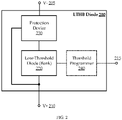
- FIG. 2 shows a block diagram of an illustrative low threshold voltage, high breakdown voltage (LTHB) diode 200, according to various embodiments.
- the LTHB diode 200 can be implemented as a two-terminal device, or as a three-terminal device.
- the LTHB diode 200 includes a low-threshold-voltage diode 220 coupled with a protection device 230, both coupled between a cathode 205 (e.g., a first terminal) and an anode 210 (e.g., a second terminal).
- the low-threshold-voltage diode 220 can be implemented as any suitable diode device having a threshold voltage that is appreciably lower than that of a typical conventional diode for the application in which the diode is being used (e.g., below 0.6 volts).
- a typical conventional diode for the application in which the diode is being used e.g., below 0.6 volts.
- the low-threshold-voltage diode 220 can be implemented using a think-oxide device, such as a diode-connected eLV T (extra-low threshold voltage) device, LV T (low threshold voltage) device, aV T (analog threshold voltage) device, or the like.
- the low-threshold-voltage diode 220 can also be implemented using a eHV T (extra-high threshold voltage) device, or a HV T (high threshold voltage) device, if such device has threshold voltages below that of the conventional diode typically used for the particular application.
- the protection device 230 can be implemented as any suitable device that, when coupled with the low-threshold-voltage diode 220, provides breakdown voltage protection to the low-threshold-voltage diode 220 without increasing the effective threshold voltage.
- so-called native devices, and/or other devices can have substantially zero, or even negative, threshold voltages.
- the LTHB diode 200 When implemented as a three-terminal device, the LTHB diode 200 includes multiple low-threshold-voltage diodes 220 (e.g., a low-threshold-voltage diode 220 bank) coupled with the protection device 230, both coupled between the cathode 205 (e.g., a first terminal) and the anode 210 (e.g., a second terminal). Further, in such an implementation, the LTHB diode 200 includes a threshold programmer 240 coupled with the low-threshold-voltage diode 220 bank.
- a threshold programmer 240 coupled with the low-threshold-voltage diode 220 bank.
- the bank of low-threshold-voltage diodes 220 can include multiple low-threshold-voltage diodes 220, each having different characteristics, including different threshold voltages.
- the threshold programmer 240 can receive an input programming signal 215, and can selectively couple one or more of the low-threshold-voltage diodes 220 in the bank with the protection device 230 responsive to the signal 215.
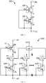
- FIG. 3 shows a circuit implementation of an illustrative low threshold voltage, high breakdown voltage (LTHB) diode 300, according to an example not falling under the present invention.
- the LTHB diode 300 can be an implementation of the two-terminal LTHB diode 200 embodiments described with reference to FIG. 2 .
- the LTHB diode 300 can include a low-threshold-voltage diode 220 and a protection device 230, coupled between a cathode 205 and an anode 210.
- the low-threshold-voltage diode 220 can be implemented as a diode-connected transistor.
- the low-threshold-voltage diode 220 is a metal-oxide semiconductor field-effect transistor (MOSFET) having a gate 222, a drain 224, and a source 226; where the drain 224 and the gate 222 coupled together.
- MOSFET metal-oxide semiconductor field-effect transistor
- the gate-to-source voltage of the transistor defines a threshold voltage above which the transistor acts like a diode with substantially quadratic current-versus-voltage (I-V) characteristics.
- the transistor when a positive voltage is applied at the anode 210 (relative to the cathode 205) that overcomes the effective threshold voltage (due to the VGS), the transistor turns on, and current is permitted to flow through the device; when a voltage is applied at the anode 210 (relative to the cathode 205) that is below the effective threshold voltage, the transistor turns off, and current is not permitted to flow.
- Some embodiments of the protection device 230 are implemented as a depletion-mode transistor.
- Depletion-mode transistors can have a substantially zero, or even negative, threshold voltage.
- the depletion-mode transistor can include a low-level P-doped silicon substrate, rather than P-well doping, to form a MOSFET channel. In effect, when the gate voltage is at zero, a conductive channel forms beneath the gate oxide layer, thereby effectively being normally on (i.e., any negative voltage, or a negative voltage exceeding a negative threshold level in some implementations, is needed to turn off the transistor).
- Some embodiments of the protection device 230 are implemented as a native (or "natural") transistor.
- the native transistor is an implementation of a depletion-mode transistor.
- the native transistor is a variety of MOSFET operating in an intermediate mode between a depletion-mode and an enhancement-mode transistor. In such instances, the native transistor typically manifests a threshold voltage at, or close to, zero volts.
- the LTHB diode 300 can be implemented by coupling the drain 224 and the gate 222 of the low-threshold-voltage diode 220 (implemented as the diode-connected, enhancement-mode MOSFET) to the anode 210; and coupling the source 226 of the low-threshold-voltage diode 220 to a drain 234 of the protection device 230 (implemented as the depletion-mode or native transistor).
- a gate 232 of the protection device 230 is coupled to the anode 210, such that the protection device 230 also permits current to flow at least while the low-threshold-voltage diode 220 is conducting in the forward direction.
- a source 236 of the protection device 230 is coupled to the cathode 205.
- FIG. 4 shows a circuit implementation of an illustrative programmable-threshold diode 400, according to various embodiments.
- the programmable-threshold diode 400 can be an implementation of the three-terminal LTHB diode 200 embodiments described with reference to FIG. 2 .
- the programmable-threshold diode 400 can include multiple low-threshold-voltage diodes 220 (illustrated as low-threshold-voltage diodes 220a..220n) and a protection device 230, coupled between a cathode 205 and an anode 210.
- Each low-threshold-voltage diode 220 can be coupled with the protection device 230 via a parallel branch, and each branch can include a switch 410 (illustrated as switches 410a..410n). Each switch 410 can be implemented in any suitable manner, for example, as a MOS transistor. Closing the switch 410 for any particular branch couples the low-threshold-voltage diode 220 in that branch with the protection device 230. In some implementations, only a single switch 410 can be closed at any time. For example, at any particular time, the effective circuit acts like the LTHB diode 300 of FIG.
- multiple switches 410 can be closed, such that multiple low-threshold-voltage diodes 220 are coupled with the protection device 230 in parallel.
- each low-threshold-voltage diode 220 has a different threshold voltage characteristic.
- the various branches can include one or more of a diode-connected eLV T (extra-low threshold voltage) device, LV T (low threshold voltage) device, aV T (analog threshold voltage) device, etc.
- each branch is shown as having only a single device implementing the low-threshold-voltage diode 220 for the branch, some embodiments can include multiple devices in each of one or more of the branches.
- the low-threshold-voltage diode 220 of a particular branch can be implemented by multiple diode-connected, low-threshold-voltage transistors in series and/or parallel.
- the branches can also include a eHV T (extra-high threshold voltage) device, a HV T (high threshold voltage) device, a light-emitting diode device, a short circuit (i.e., such that the circuit operates only as the protection device 230 when the switch 410 of the corresponding branch is closed), etc.
- the threshold voltage e.g., and possibly other characteristics
- the switches 410 can be controlled in any suitable manner. As illustrated, embodiments can include a threshold programmer 240 that controls the switches 410 responsive to an input programming signal 215.
- the threshold programmer 240 can be implemented as a de-multiplexer, or the like, with the input programming signal 215 used as a digital selector.
- the input programming signal 215 i.e., one or more bits
- the input programming signal 215 can effectively couple an input voltage level with a selected one of multiple outputs, and each output can be coupled with a respective one or more of the switches 410.
- the programmable-threshold diode 400 is implemented as an integrated circuit having a housing with external interface structures (e.g., a set of pins, a ball grid array, etc.); and the switches 410 are coupled with one or more of the external interface structures.
- the threshold programmer 240 can be used to assert a signal at a particular external interface structure (e.g., by applying a particular voltage level), causes one or more switches 410 to turn on or off.
- the input programming signal 215 received by the threshold programmer 240 can be implemented as a plurality of signals (e.g., the single signal path represents a bus, or a set of signals), each coupled with an external interface structure (and corresponding to a respective one or more of the switches 410.
- the threshold programmer 240 can be implemented as a dip switch, or other external mechanical switch, coupled with the programmable-threshold diode 400.
- mechanically setting the threshold programmer 240 can effectively program the threshold voltage of the programmable-threshold diode 400.
- the programming can be manual, and there may not be an input programming signal 215.
- FIG. 5 shows a flow diagram of an illustrative method 500 for programming a threshold voltage of a diode device, according to various embodiments.
- Embodiments of the method 500 begin at stage 504 by first enabling, at a first time, a first switch of multiple switches. Each switch is configured to selectively enable one of multiple parallel branches, each having one of multiple low-threshold-voltage diodes.
- the first enabling at stage 504 couples a first of the low-threshold-voltage diodes to a protection device.
- the first of the low-threshold-voltage diodes has a first positive threshold voltage (e.g., 0.3 volts), and the protection device has a non-positive threshold voltage (e.g., 0 volts, or -0.1 volts).
- embodiments can second enable, at a second time, a second of the switches. The second enabling couples a second of the low-threshold-voltage diodes to the protection device.
- the second of the low-threshold-voltage diodes has a second positive threshold voltage that is different from the first positive threshold voltage.
- the first enabling at stage 504 involves applying a first input programming signal at a signal input of a threshold programmer at the first time.
- the threshold programmer can have multiple switch outputs each to enable a corresponding one of the switches responsive to the signal input, such that applying the first input programming signal enables the first switch.
- the second enabling at stage 508 can involve applying a second input programming signal (different from the first input programming signal) at the signal input of a threshold programmer at the second time.
- the threshold programmer is configured, such that applying the second input programming signal enables the second switch.
- a first element, component, discussed below could be termed a second element, component, without departing from the teachings of the present invention.
- the terms “logic low,” “low state,” “low level,” “logic low level,” “low,” or “0” are used interchangeably.
- logic high “high state,” “high level,” “logic high level,” “high,” or “1” are used interchangeably.
- the terms “a”, “an” and “the” may include singular and plural references. It will be further understood that the terms “comprising”, “including”, having” and variants thereof, when used in this specification, specify the presence of stated features, steps, operations, elements, and/or components, but do not preclude the presence or addition of one or more other features, steps, operations, elements, components, and/or groups thereof. In contrast, the term “consisting of' when used in this specification, specifies the stated features, steps, operations, elements, and/or components, and precludes additional features, steps, operations, elements and/or components. Furthermore, as used herein, the words “and/or” may refer to and encompass any possible combinations of one or more of the associated listed items.
Landscapes
- Semiconductor Integrated Circuits (AREA)
Claims (8)
- Dispositif à diode à seuil programmable (400), comprenantune borne de cathode (205) ;une borne d'anode (210) ;un dispositif de protection (230) ayant une entrée de commande de protection couplée à la borne d'anode (210), de telle sorte que l'application, à la borne d'anode (210), d'un niveau de tension dépassant un niveau de tension de seuil de protection permette à un courant de passer à travers le dispositif de protection (230), le niveau de tension de seuil de protection étant non positif ; etune batterie de diodes à basse tension de seuil (220) comprenant une pluralité de chemins parallèles, chaque chemin parallèle comprenant :un commutateur d'une pluralité de commutateurs (410) ; etun dispositif à basse tension de seuil d'une pluralité de dispositifs à basse tension de seuil, chaque dispositif à basse tension de seuil ayant une tension de seuil respective qui est différente de celle d'au moins certains autres de la pluralité de dispositifs à basse tension de seuil, le dispositif à basse tension de seuil étant couplé entre la borne d'anode (210) et le commutateur (410), et ayant une entrée de commande de diode couplée à la borne d'anode (210), de telle sorte que l'application, à la borne d'anode (210), d'un niveau de tension dépassant la tension de seuil respective permette à un courant de passer à travers le dispositif à basse tension de seuil,dans lequel la fermeture du commutateur (410) couple le dispositif à basse tension de seuil au dispositif de protection (230) ;dans lequel le dispositif de protection (230) est un transistor à semi-conducteur à oxyde de métal à appauvrissement ayant une grille (232), un drain (234), et une source (236) ;la grille (232) du dispositif de protection (230) est l'entrée de commande de protection couplée à la borne d'anode (210) ;la source (236) du dispositif de protection (230) est couplée à la borne de cathode (205) ; etle drain (234) du dispositif de protection (230) est couplé à la pluralité de commutateurs (410) ; etdans lequel, pour chaque chemin parallèle :le dispositif à basse tension de seuil est un transistor à semi-conducteur à oxyde de métal à enrichissement, connecté à diode, ayant une grille (222), un drain (224), et une source (226) ;la grille (222) du dispositif à basse tension de seuil est l'entrée de commande de diode couplée à la borne d'anode (210) ;le drain (224) du dispositif à basse tension de seuil est couplé à la borne d'anode (210) ; etla source (226) du dispositif à basse tension de seuil est couplée au commutateur (410).
- Dispositif à diode à seuil programmable (400) selon la revendication 1, comprenant en outre :un programmateur de seuil (240) ayant une entrée de signal et une pluralité de sorties de commutateur, l'entrée de signal étant destinée à recevoir un signal de programmation d'entrée (215), et la pluralité de sorties de commutateur étant couplées à la pluralité de commutateurs (410), afin de commander un état de la pluralité de commutateurs (410) en réponse au signal de programmation d'entrée (215) ;dans lequel :le programmateur de seuil (240) est un démultiplexeur ayant une entrée de commande de commutateur destinée à recevoir un signal d'affirmation de commutateur ; etle démultiplexeur est destiné à coupler l'entrée de commande de commutateur à une de la pluralité de sorties de commutateur conformément au signal de programmation d'entrée (215), de telle sorte qu'un sélectionné de la pluralité de commutateurs (410) soit affirmé par le signal d'affirmation de commutateur conformément au signal de programmation d'entrée (215).
- Dispositif à diode à seuil programmable (400) selon la revendication 1 ou 2, comprenant en outre :un logement de circuit intégré ayant une pluralité de structures d'interface intégrées avec celui-ci, dans lequel :le logement de circuit intégré a, logé dans celui-ci, le dispositif de protection (230) et la batterie de diodes à basse tension de seuil (220) ;une première de la pluralité de structures d'interface est couplée à la borne de cathode (205) ; etune seconde de la pluralité de structures d'interface est couplée à la borne d'anode (210) ;dans lequel chacune d'un ensemble de la pluralité de structures d'interface est couplée à une commande de commutateur d'un respectif de la pluralité de commutateurs (410), de telle sorte qu'un état de chacun de la pluralité de commutateurs (410) soit commandable conformément à un signal appliqué à une de l'ensemble de la pluralité de structures d'interface.
- Dispositif à diode à seuil programmable (400) selon la revendication 3, comprenant en outre :un programmateur de seuil (240) ayant une entrée de signal et une pluralité de sorties de commutateur, l'entrée de signal étant destinée à recevoir un signal de programmation d'entrée (215), et la pluralité de sorties de commutateur étant couplées à la pluralité de commutateurs (410), afin de commander un état de la pluralité de commutateurs (410) en réponse au signal de programmation d'entrée (215),dans lequel l'entrée de signal est couplée à au moins une de la pluralité de structures d'interface.
- Dispositif à diode à seuil programmable (400) selon l'une quelconque des revendications 1 à 4, dans lequel :
la tension de seuil respective de chaque dispositif à basse tension de seuil est différente de celle de tous les autres de la pluralité de dispositifs à basse tension de seuil. - Dispositif à diode à seuil programmable (400) selon l'une quelconque des revendications 1 à 5, dans lequel :le dispositif de protection (230) est un transistor à appauvrissement, le niveau de tension de seuil de protection étant négatif ; oule dispositif de protection (230) est un transistor natif, le niveau de tension de seuil de protection étant sensiblement zéro.
- Procédé (500) pour programmer une tension de seuil d'un dispositif de diode (400) selon l'une quelconque des revendications 1 à 6, le procédé comprenant :une première activation (504), à un premier instant, d'un premier commutateur d'une pluralité de commutateurs, chacun de la pluralité de commutateurs étant configuré pour sélectivement activer un d'une pluralité de chemins parallèles,dans lequel chaque chemin parallèle comprend un dispositif à basse tension de seuil d'une pluralité de dispositifs à basse tension de seuil, etdans lequel la première activation couple un premier de la pluralité de dispositifs à basse tension de seuil à un dispositif de protection, le premier de la pluralité de dispositifs à basse tension de seuil ayant une première tension de seuil positive, et le dispositif de protection ayant une tension de seuil non positive ; etune seconde activation (508), à un second instant, d'un second commutateur de la pluralité de commutateurs,dans lequel la seconde activation couple un second de la pluralité de dispositifs à basse tension de seuil au dispositif de protection, le second de la pluralité de dispositifs à basse tension de seuil ayant une seconde tension de seuil positive qui est différente de la première tension de seuil positive.
- Procédé (500) selon la revendication 7, dans lequel :la première activation (504) comprend l'application d'un premier signal de programmation d'entrée à une entrée de signal d'un programmateur de seuil au premier instant ;la seconde activation (508) comprend l'application d'un second signal de programmation d'entrée à l'entrée de signal du programmateur de seuil au second instant ; etle programmateur de seuil a une pluralité de sorties de commutateur, chacune pour activer un correspondant de la pluralité de commutateurs en réponse à l'entrée de signal, de telle sorte que l'application du premier signal de programmation d'entrée active le premier commutateur, et l'application du second signal de programmation d'entrée active le second commutateur.
Applications Claiming Priority (2)
| Application Number | Priority Date | Filing Date | Title |
|---|---|---|---|
| US16/282,264 US11190177B2 (en) | 2019-02-21 | 2019-02-21 | Diode with low threshold voltage and high breakdown voltage |
| PCT/CN2019/104119 WO2020168704A1 (fr) | 2019-02-21 | 2019-09-03 | Diode à faible tension de seuil et à tension de claquage élevée |
Publications (3)
| Publication Number | Publication Date |
|---|---|
| EP3718211A1 EP3718211A1 (fr) | 2020-10-07 |
| EP3718211A4 EP3718211A4 (fr) | 2020-10-21 |
| EP3718211B1 true EP3718211B1 (fr) | 2022-05-04 |
Family
ID=70480059
Family Applications (1)
| Application Number | Title | Priority Date | Filing Date |
|---|---|---|---|
| EP19868172.8A Not-in-force EP3718211B1 (fr) | 2019-02-21 | 2019-09-03 | Diode à faible tension de seuil et à tension de claquage élevée |
Country Status (4)
| Country | Link |
|---|---|
| US (1) | US11190177B2 (fr) |
| EP (1) | EP3718211B1 (fr) |
| CN (1) | CN110959193B (fr) |
| WO (1) | WO2020168704A1 (fr) |
Citations (1)
| Publication number | Priority date | Publication date | Assignee | Title |
|---|---|---|---|---|
| JP2013219306A (ja) * | 2012-04-12 | 2013-10-24 | Advanced Power Device Research Association | 半導体ダイオード装置 |
Family Cites Families (39)
| Publication number | Priority date | Publication date | Assignee | Title |
|---|---|---|---|---|
| US3404293A (en) * | 1966-03-25 | 1968-10-01 | Bell Telephone Labor Inc | Thyristor switch utilizing series diodes to improve dynamic breakdown capability and reduce time to restore for ward blocking |
| US3444398A (en) * | 1966-05-10 | 1969-05-13 | Bell Telephone Labor Inc | Thyristor switch utilizing diodes to improve recovery time |
| US3941940A (en) * | 1974-12-06 | 1976-03-02 | Rca Corporation | Transient suppressor |
| US4158866A (en) * | 1977-11-30 | 1979-06-19 | Exxon Research & Engineering Co. | Protection circuit for transistorized switch |
| US4374303A (en) * | 1981-03-27 | 1983-02-15 | Gte Automatic Electric Laboratories, Inc. | Power supply control circuit for subscriber carrier telephone system |
| US4380687A (en) * | 1981-03-27 | 1983-04-19 | Gte Automatic Electric Laboratories, Inc. | Power supply control circuit for subscriber carrier telephone system |
| US4419586A (en) * | 1981-08-27 | 1983-12-06 | Motorola, Inc. | Solid-state relay and regulator |
| JPH09293836A (ja) * | 1996-04-25 | 1997-11-11 | Rohm Co Ltd | 半導体装置 |
| IT1312287B1 (it) * | 1999-05-03 | 2002-04-10 | St Microelectronics Srl | Circuito comparatore per segnali positivi e negativi,avente consumonullo,adatto per dispositivi a singola alimentazione positiva |
| DE10217935B4 (de) * | 2001-04-23 | 2007-06-28 | Fuji Electric Co., Ltd., Kawasaki | Halbleiterbauteil |
| JP4059874B2 (ja) * | 2004-09-30 | 2008-03-12 | 富士通株式会社 | 整流回路 |
| JP2007325468A (ja) * | 2006-06-05 | 2007-12-13 | Toshiba Corp | 電源回路 |
| US20080061843A1 (en) * | 2006-09-11 | 2008-03-13 | Asier Goikoetxea Yanci | Detecting voltage glitches |
| JP2008130994A (ja) * | 2006-11-24 | 2008-06-05 | Toshiba Corp | 静電保護回路 |
| US7990108B2 (en) * | 2007-05-14 | 2011-08-02 | Atmel Corporation | Charge detector |
| JP2009182107A (ja) | 2008-01-30 | 2009-08-13 | Furukawa Electric Co Ltd:The | 半導体装置 |
| US8004806B2 (en) * | 2009-05-04 | 2011-08-23 | United Silicon Carbide, Inc. | Solid-state disconnect device |
| US20110050198A1 (en) * | 2009-09-01 | 2011-03-03 | Zhiwei Dong | Low-power voltage regulator |
| JP2012004254A (ja) | 2010-06-15 | 2012-01-05 | Panasonic Corp | ダイオード回路 |
| IT1405693B1 (it) * | 2011-02-22 | 2014-01-24 | Elettromeccaniche P Torresan S R L Costruzioni | Dispositivo di protezione da sovratensione e fulminazione per un apparecchio elettrico |
| JP2014027253A (ja) | 2012-06-22 | 2014-02-06 | Toshiba Corp | 整流回路 |
| US8995158B2 (en) * | 2012-07-11 | 2015-03-31 | Infineon Technologies Dresden Gmbh | Circuit arrangement with a rectifier circuit |
| US9013848B2 (en) * | 2012-09-27 | 2015-04-21 | Alpha And Omega Semiconductor Incorporated | Active clamp protection circuit for power semiconductor device for high frequency switching |
| EP2736171A1 (fr) * | 2012-11-23 | 2014-05-28 | Nxp B.V. | Dispositifs à semi-conducteurs cascadés |
| US9178507B2 (en) * | 2012-11-28 | 2015-11-03 | Analog Devices, Inc. | Apparatus and methods for ultrasound transmit switching |
| US8917135B2 (en) * | 2013-05-14 | 2014-12-23 | Infineon Technologies Austria Ag | Circuit with a plurality of diodes and method for controlling such a circuit |
| JP6213719B2 (ja) * | 2013-08-08 | 2017-10-18 | セイコーエプソン株式会社 | 入力保護回路、電子デバイス、リアルタイムクロックモジュール、電子機器及び移動体 |
| US9397682B2 (en) * | 2014-04-25 | 2016-07-19 | Analog Devices, Inc. | Reference buffer with wide trim range |
| JP6223918B2 (ja) * | 2014-07-07 | 2017-11-01 | 株式会社東芝 | 半導体装置 |
| US9628081B2 (en) * | 2014-08-12 | 2017-04-18 | Xilinx, Inc. | Interconnect circuits having low threshold voltage P-channel transistors for a programmable integrated circuit |
| JP6415265B2 (ja) * | 2014-11-19 | 2018-10-31 | キヤノン株式会社 | 保護回路 |
| GB2533344B (en) * | 2014-12-17 | 2019-11-06 | Intelligent Energy Saving Company Ltd | A circuit for a voltage power optimiser |
| US9837399B2 (en) * | 2015-07-24 | 2017-12-05 | Semiconductor Components Industries, Llc | Cascode configured semiconductor component and method |
| ITUB20159684A1 (it) * | 2015-12-22 | 2017-06-22 | St Microelectronics Srl | Interruttore elettronico, dispositivo e procedimento corrispondenti |
| ITUA20162889A1 (it) * | 2016-04-26 | 2017-10-26 | St Microelectronics Srl | Circuito di commutazione, relativo procedimento e circuito integrato |
| US10854718B2 (en) * | 2017-02-21 | 2020-12-01 | Semiconductor Components Industries, Llc | Method of forming a semiconductor device |
| GB2564482B (en) * | 2017-07-14 | 2021-02-10 | Cambridge Entpr Ltd | A power semiconductor device with a double gate structure |
| CN107707235A (zh) | 2017-08-11 | 2018-02-16 | 南京博兰得电子科技有限公司 | 一种组合开关 |
| US20190296737A1 (en) * | 2018-03-23 | 2019-09-26 | Semiconductor Components Industries, Llc | Diode circuit for efficient operation |
-
2019
- 2019-02-21 US US16/282,264 patent/US11190177B2/en active Active
- 2019-09-03 WO PCT/CN2019/104119 patent/WO2020168704A1/fr not_active Ceased
- 2019-09-03 EP EP19868172.8A patent/EP3718211B1/fr not_active Not-in-force
- 2019-09-03 CN CN201980002366.3A patent/CN110959193B/zh active Active
Patent Citations (1)
| Publication number | Priority date | Publication date | Assignee | Title |
|---|---|---|---|---|
| JP2013219306A (ja) * | 2012-04-12 | 2013-10-24 | Advanced Power Device Research Association | 半導体ダイオード装置 |
Also Published As
| Publication number | Publication date |
|---|---|
| WO2020168704A1 (fr) | 2020-08-27 |
| CN110959193A (zh) | 2020-04-03 |
| CN110959193B (zh) | 2023-09-05 |
| EP3718211A4 (fr) | 2020-10-21 |
| US11190177B2 (en) | 2021-11-30 |
| US20200274529A1 (en) | 2020-08-27 |
| EP3718211A1 (fr) | 2020-10-07 |
Similar Documents
| Publication | Publication Date | Title |
|---|---|---|
| US20160372920A1 (en) | Integrated esd protection circuits in gan | |
| US9472948B2 (en) | On chip reverse polarity protection compliant with ISO and ESD requirements | |
| US10756720B2 (en) | Driver circuit for electronic switch | |
| US7683696B1 (en) | Open-drain output buffer for single-voltage-supply CMOS | |
| CN110838836B (zh) | 容错低泄漏开关 | |
| CN113196663A (zh) | 共源共栅复合开关压摆率控制 | |
| US20190006842A1 (en) | Protection circuit | |
| US20100109743A1 (en) | Level shifter having native transistors | |
| US9912332B2 (en) | Semiconductor device | |
| JP2006261679A (ja) | 低電圧用esd保護回路 | |
| EP0656690A2 (fr) | Circuit à transistors | |
| US9991253B2 (en) | Protection element, protection circuit, and semiconductor integrated circuit | |
| US11195825B2 (en) | Multi-diode semiconductor device and method of operation therefor | |
| US9559681B2 (en) | Semiconductor integrated circuit device | |
| US8581656B2 (en) | Transmission gate and control circuit for transmission gate inputs | |
| US9407242B2 (en) | Voltage level shifter for high voltage applications | |
| CN110784199A (zh) | 集成电路、驱动电路及其操作方法 | |
| US11190177B2 (en) | Diode with low threshold voltage and high breakdown voltage | |
| EP3309836A1 (fr) | Circuit de décharge électrostatique | |
| US12395165B2 (en) | Apparatus and methods to control well bias in a semiconductor device | |
| EP0204762B1 (fr) | Circuit logique integré | |
| US6061219A (en) | Device for the protection of an electrical load and power supply circuit having such a device | |
| US11658658B2 (en) | High-voltage switches | |
| JP2003108245A (ja) | 基準電圧回路 | |
| US7402869B2 (en) | Apparatus and method for breakdown protection of a source follower circuit |
Legal Events
| Date | Code | Title | Description |
|---|---|---|---|
| STAA | Information on the status of an ep patent application or granted ep patent |
Free format text: STATUS: UNKNOWN |
|
| STAA | Information on the status of an ep patent application or granted ep patent |
Free format text: STATUS: THE INTERNATIONAL PUBLICATION HAS BEEN MADE |
|
| PUAI | Public reference made under article 153(3) epc to a published international application that has entered the european phase |
Free format text: ORIGINAL CODE: 0009012 |
|
| STAA | Information on the status of an ep patent application or granted ep patent |
Free format text: STATUS: REQUEST FOR EXAMINATION WAS MADE |
|
| 17P | Request for examination filed |
Effective date: 20200409 |
|
| AK | Designated contracting states |
Kind code of ref document: A1 Designated state(s): AL AT BE BG CH CY CZ DE DK EE ES FI FR GB GR HR HU IE IS IT LI LT LU LV MC MK MT NL NO PL PT RO RS SE SI SK SM TR |
|
| AX | Request for extension of the european patent |
Extension state: BA ME |
|
| A4 | Supplementary search report drawn up and despatched |
Effective date: 20200923 |
|
| RIC1 | Information provided on ipc code assigned before grant |
Ipc: H03K 17/081 20060101ALI20200917BHEP Ipc: H03K 17/74 20060101AFI20200917BHEP Ipc: H03K 17/72 20060101ALI20200917BHEP Ipc: H03K 17/76 20060101ALI20200917BHEP Ipc: H03K 17/10 20060101ALI20200917BHEP |
|
| STAA | Information on the status of an ep patent application or granted ep patent |
Free format text: STATUS: EXAMINATION IS IN PROGRESS |
|
| 17Q | First examination report despatched |
Effective date: 20210830 |
|
| GRAP | Despatch of communication of intention to grant a patent |
Free format text: ORIGINAL CODE: EPIDOSNIGR1 |
|
| GRAS | Grant fee paid |
Free format text: ORIGINAL CODE: EPIDOSNIGR3 |
|
| STAA | Information on the status of an ep patent application or granted ep patent |
Free format text: STATUS: GRANT OF PATENT IS INTENDED |
|
| DAV | Request for validation of the european patent (deleted) | ||
| DAX | Request for extension of the european patent (deleted) | ||
| INTG | Intention to grant announced |
Effective date: 20220302 |
|
| GRAA | (expected) grant |
Free format text: ORIGINAL CODE: 0009210 |
|
| STAA | Information on the status of an ep patent application or granted ep patent |
Free format text: STATUS: THE PATENT HAS BEEN GRANTED |
|
| AK | Designated contracting states |
Kind code of ref document: B1 Designated state(s): AL AT BE BG CH CY CZ DE DK EE ES FI FR GB GR HR HU IE IS IT LI LT LU LV MC MK MT NL NO PL PT RO RS SE SI SK SM TR |
|
| REG | Reference to a national code |
Ref country code: GB Ref legal event code: FG4D |
|
| REG | Reference to a national code |
Ref country code: CH Ref legal event code: EP |
|
| REG | Reference to a national code |
Ref country code: AT Ref legal event code: REF Ref document number: 1490223 Country of ref document: AT Kind code of ref document: T Effective date: 20220515 |
|
| REG | Reference to a national code |
Ref country code: IE Ref legal event code: FG4D Ref country code: DE Ref legal event code: R096 Ref document number: 602019014676 Country of ref document: DE |
|
| REG | Reference to a national code |
Ref country code: LT Ref legal event code: MG9D |
|
| GRAP | Despatch of communication of intention to grant a patent |
Free format text: ORIGINAL CODE: EPIDOSNIGR1 |
|
| REG | Reference to a national code |
Ref country code: NL Ref legal event code: MP Effective date: 20220504 |
|
| REG | Reference to a national code |
Ref country code: AT Ref legal event code: MK05 Ref document number: 1490223 Country of ref document: AT Kind code of ref document: T Effective date: 20220504 |
|
| PG25 | Lapsed in a contracting state [announced via postgrant information from national office to epo] |
Ref country code: SE Free format text: LAPSE BECAUSE OF FAILURE TO SUBMIT A TRANSLATION OF THE DESCRIPTION OR TO PAY THE FEE WITHIN THE PRESCRIBED TIME-LIMIT Effective date: 20220504 Ref country code: PT Free format text: LAPSE BECAUSE OF FAILURE TO SUBMIT A TRANSLATION OF THE DESCRIPTION OR TO PAY THE FEE WITHIN THE PRESCRIBED TIME-LIMIT Effective date: 20220905 Ref country code: NO Free format text: LAPSE BECAUSE OF FAILURE TO SUBMIT A TRANSLATION OF THE DESCRIPTION OR TO PAY THE FEE WITHIN THE PRESCRIBED TIME-LIMIT Effective date: 20220804 Ref country code: NL Free format text: LAPSE BECAUSE OF FAILURE TO SUBMIT A TRANSLATION OF THE DESCRIPTION OR TO PAY THE FEE WITHIN THE PRESCRIBED TIME-LIMIT Effective date: 20220504 Ref country code: LT Free format text: LAPSE BECAUSE OF FAILURE TO SUBMIT A TRANSLATION OF THE DESCRIPTION OR TO PAY THE FEE WITHIN THE PRESCRIBED TIME-LIMIT Effective date: 20220504 Ref country code: HR Free format text: LAPSE BECAUSE OF FAILURE TO SUBMIT A TRANSLATION OF THE DESCRIPTION OR TO PAY THE FEE WITHIN THE PRESCRIBED TIME-LIMIT Effective date: 20220504 Ref country code: GR Free format text: LAPSE BECAUSE OF FAILURE TO SUBMIT A TRANSLATION OF THE DESCRIPTION OR TO PAY THE FEE WITHIN THE PRESCRIBED TIME-LIMIT Effective date: 20220805 Ref country code: FI Free format text: LAPSE BECAUSE OF FAILURE TO SUBMIT A TRANSLATION OF THE DESCRIPTION OR TO PAY THE FEE WITHIN THE PRESCRIBED TIME-LIMIT Effective date: 20220504 Ref country code: ES Free format text: LAPSE BECAUSE OF FAILURE TO SUBMIT A TRANSLATION OF THE DESCRIPTION OR TO PAY THE FEE WITHIN THE PRESCRIBED TIME-LIMIT Effective date: 20220504 Ref country code: BG Free format text: LAPSE BECAUSE OF FAILURE TO SUBMIT A TRANSLATION OF THE DESCRIPTION OR TO PAY THE FEE WITHIN THE PRESCRIBED TIME-LIMIT Effective date: 20220804 Ref country code: AT Free format text: LAPSE BECAUSE OF FAILURE TO SUBMIT A TRANSLATION OF THE DESCRIPTION OR TO PAY THE FEE WITHIN THE PRESCRIBED TIME-LIMIT Effective date: 20220504 |
|
| PG25 | Lapsed in a contracting state [announced via postgrant information from national office to epo] |
Ref country code: RS Free format text: LAPSE BECAUSE OF FAILURE TO SUBMIT A TRANSLATION OF THE DESCRIPTION OR TO PAY THE FEE WITHIN THE PRESCRIBED TIME-LIMIT Effective date: 20220504 Ref country code: PL Free format text: LAPSE BECAUSE OF FAILURE TO SUBMIT A TRANSLATION OF THE DESCRIPTION OR TO PAY THE FEE WITHIN THE PRESCRIBED TIME-LIMIT Effective date: 20220504 Ref country code: LV Free format text: LAPSE BECAUSE OF FAILURE TO SUBMIT A TRANSLATION OF THE DESCRIPTION OR TO PAY THE FEE WITHIN THE PRESCRIBED TIME-LIMIT Effective date: 20220504 Ref country code: IS Free format text: LAPSE BECAUSE OF FAILURE TO SUBMIT A TRANSLATION OF THE DESCRIPTION OR TO PAY THE FEE WITHIN THE PRESCRIBED TIME-LIMIT Effective date: 20220904 |
|
| PG25 | Lapsed in a contracting state [announced via postgrant information from national office to epo] |
Ref country code: SM Free format text: LAPSE BECAUSE OF FAILURE TO SUBMIT A TRANSLATION OF THE DESCRIPTION OR TO PAY THE FEE WITHIN THE PRESCRIBED TIME-LIMIT Effective date: 20220504 Ref country code: SK Free format text: LAPSE BECAUSE OF FAILURE TO SUBMIT A TRANSLATION OF THE DESCRIPTION OR TO PAY THE FEE WITHIN THE PRESCRIBED TIME-LIMIT Effective date: 20220504 Ref country code: RO Free format text: LAPSE BECAUSE OF FAILURE TO SUBMIT A TRANSLATION OF THE DESCRIPTION OR TO PAY THE FEE WITHIN THE PRESCRIBED TIME-LIMIT Effective date: 20220504 Ref country code: EE Free format text: LAPSE BECAUSE OF FAILURE TO SUBMIT A TRANSLATION OF THE DESCRIPTION OR TO PAY THE FEE WITHIN THE PRESCRIBED TIME-LIMIT Effective date: 20220504 Ref country code: DK Free format text: LAPSE BECAUSE OF FAILURE TO SUBMIT A TRANSLATION OF THE DESCRIPTION OR TO PAY THE FEE WITHIN THE PRESCRIBED TIME-LIMIT Effective date: 20220504 Ref country code: CZ Free format text: LAPSE BECAUSE OF FAILURE TO SUBMIT A TRANSLATION OF THE DESCRIPTION OR TO PAY THE FEE WITHIN THE PRESCRIBED TIME-LIMIT Effective date: 20220504 |
|
| REG | Reference to a national code |
Ref country code: DE Ref legal event code: R097 Ref document number: 602019014676 Country of ref document: DE |
|
| PLBE | No opposition filed within time limit |
Free format text: ORIGINAL CODE: 0009261 |
|
| STAA | Information on the status of an ep patent application or granted ep patent |
Free format text: STATUS: NO OPPOSITION FILED WITHIN TIME LIMIT |
|
| PG25 | Lapsed in a contracting state [announced via postgrant information from national office to epo] |
Ref country code: AL Free format text: LAPSE BECAUSE OF FAILURE TO SUBMIT A TRANSLATION OF THE DESCRIPTION OR TO PAY THE FEE WITHIN THE PRESCRIBED TIME-LIMIT Effective date: 20220504 |
|
| 26N | No opposition filed |
Effective date: 20230207 |
|
| PG25 | Lapsed in a contracting state [announced via postgrant information from national office to epo] |
Ref country code: MC Free format text: LAPSE BECAUSE OF FAILURE TO SUBMIT A TRANSLATION OF THE DESCRIPTION OR TO PAY THE FEE WITHIN THE PRESCRIBED TIME-LIMIT Effective date: 20220504 |
|
| REG | Reference to a national code |
Ref country code: CH Ref legal event code: PL |
|
| REG | Reference to a national code |
Ref country code: BE Ref legal event code: MM Effective date: 20220930 |
|
| PG25 | Lapsed in a contracting state [announced via postgrant information from national office to epo] |
Ref country code: SI Free format text: LAPSE BECAUSE OF FAILURE TO SUBMIT A TRANSLATION OF THE DESCRIPTION OR TO PAY THE FEE WITHIN THE PRESCRIBED TIME-LIMIT Effective date: 20220504 |
|
| PG25 | Lapsed in a contracting state [announced via postgrant information from national office to epo] |
Ref country code: LU Free format text: LAPSE BECAUSE OF NON-PAYMENT OF DUE FEES Effective date: 20220903 |
|
| PG25 | Lapsed in a contracting state [announced via postgrant information from national office to epo] |
Ref country code: LI Free format text: LAPSE BECAUSE OF NON-PAYMENT OF DUE FEES Effective date: 20220930 Ref country code: IE Free format text: LAPSE BECAUSE OF NON-PAYMENT OF DUE FEES Effective date: 20220903 Ref country code: FR Free format text: LAPSE BECAUSE OF NON-PAYMENT OF DUE FEES Effective date: 20220930 Ref country code: CH Free format text: LAPSE BECAUSE OF NON-PAYMENT OF DUE FEES Effective date: 20220930 |
|
| PG25 | Lapsed in a contracting state [announced via postgrant information from national office to epo] |
Ref country code: BE Free format text: LAPSE BECAUSE OF NON-PAYMENT OF DUE FEES Effective date: 20220930 |
|
| PG25 | Lapsed in a contracting state [announced via postgrant information from national office to epo] |
Ref country code: IT Free format text: LAPSE BECAUSE OF FAILURE TO SUBMIT A TRANSLATION OF THE DESCRIPTION OR TO PAY THE FEE WITHIN THE PRESCRIBED TIME-LIMIT Effective date: 20220504 |
|
| PG25 | Lapsed in a contracting state [announced via postgrant information from national office to epo] |
Ref country code: CY Free format text: LAPSE BECAUSE OF FAILURE TO SUBMIT A TRANSLATION OF THE DESCRIPTION OR TO PAY THE FEE WITHIN THE PRESCRIBED TIME-LIMIT Effective date: 20220504 |
|
| PG25 | Lapsed in a contracting state [announced via postgrant information from national office to epo] |
Ref country code: MK Free format text: LAPSE BECAUSE OF FAILURE TO SUBMIT A TRANSLATION OF THE DESCRIPTION OR TO PAY THE FEE WITHIN THE PRESCRIBED TIME-LIMIT Effective date: 20220504 Ref country code: HU Free format text: LAPSE BECAUSE OF FAILURE TO SUBMIT A TRANSLATION OF THE DESCRIPTION OR TO PAY THE FEE WITHIN THE PRESCRIBED TIME-LIMIT; INVALID AB INITIO Effective date: 20190903 |
|
| PG25 | Lapsed in a contracting state [announced via postgrant information from national office to epo] |
Ref country code: TR Free format text: LAPSE BECAUSE OF FAILURE TO SUBMIT A TRANSLATION OF THE DESCRIPTION OR TO PAY THE FEE WITHIN THE PRESCRIBED TIME-LIMIT Effective date: 20220504 |
|
| PG25 | Lapsed in a contracting state [announced via postgrant information from national office to epo] |
Ref country code: MT Free format text: LAPSE BECAUSE OF FAILURE TO SUBMIT A TRANSLATION OF THE DESCRIPTION OR TO PAY THE FEE WITHIN THE PRESCRIBED TIME-LIMIT Effective date: 20220504 |
|
| PGFP | Annual fee paid to national office [announced via postgrant information from national office to epo] |
Ref country code: DE Payment date: 20240918 Year of fee payment: 6 |
|
| PGFP | Annual fee paid to national office [announced via postgrant information from national office to epo] |
Ref country code: GB Payment date: 20240920 Year of fee payment: 6 |
|
| PG25 | Lapsed in a contracting state [announced via postgrant information from national office to epo] |
Ref country code: BG Free format text: LAPSE BECAUSE OF FAILURE TO SUBMIT A TRANSLATION OF THE DESCRIPTION OR TO PAY THE FEE WITHIN THE PRESCRIBED TIME-LIMIT Effective date: 20220504 |
|
| PG25 | Lapsed in a contracting state [announced via postgrant information from national office to epo] |
Ref country code: BG Free format text: LAPSE BECAUSE OF FAILURE TO SUBMIT A TRANSLATION OF THE DESCRIPTION OR TO PAY THE FEE WITHIN THE PRESCRIBED TIME-LIMIT Effective date: 20220504 |
|
| REG | Reference to a national code |
Ref country code: DE Ref legal event code: R119 Ref document number: 602019014676 Country of ref document: DE |
|
| GBPC | Gb: european patent ceased through non-payment of renewal fee |
Effective date: 20250903 |
|
| PG25 | Lapsed in a contracting state [announced via postgrant information from national office to epo] |
Ref country code: GB Free format text: LAPSE BECAUSE OF NON-PAYMENT OF DUE FEES Effective date: 20250903 |
|
| PG25 | Lapsed in a contracting state [announced via postgrant information from national office to epo] |
Ref country code: DE Free format text: LAPSE BECAUSE OF NON-PAYMENT OF DUE FEES Effective date: 20260401 |