EP3718672A2 - Redresseur pour un transformateur de soudage d'un dispositif de soudage et procédé de fabrication d'un tel redresseur - Google Patents
Redresseur pour un transformateur de soudage d'un dispositif de soudage et procédé de fabrication d'un tel redresseur Download PDFInfo
- Publication number
- EP3718672A2 EP3718672A2 EP20160577.1A EP20160577A EP3718672A2 EP 3718672 A2 EP3718672 A2 EP 3718672A2 EP 20160577 A EP20160577 A EP 20160577A EP 3718672 A2 EP3718672 A2 EP 3718672A2
- Authority
- EP
- European Patent Office
- Prior art keywords
- welding
- rectifier
- transformer
- semiconductor modules
- central part
- Prior art date
- Legal status (The legal status is an assumption and is not a legal conclusion. Google has not performed a legal analysis and makes no representation as to the accuracy of the status listed.)
- Granted
Links
Images



Classifications
-
- B—PERFORMING OPERATIONS; TRANSPORTING
- B23—MACHINE TOOLS; METAL-WORKING NOT OTHERWISE PROVIDED FOR
- B23K—SOLDERING OR UNSOLDERING; WELDING; CLADDING OR PLATING BY SOLDERING OR WELDING; CUTTING BY APPLYING HEAT LOCALLY, e.g. FLAME CUTTING; WORKING BY LASER BEAM
- B23K11/00—Resistance welding; Severing by resistance heating
- B23K11/24—Electric supply or control circuits therefor
-
- H—ELECTRICITY
- H02—GENERATION; CONVERSION OR DISTRIBUTION OF ELECTRIC POWER
- H02M—APPARATUS FOR CONVERSION BETWEEN AC AND AC, BETWEEN AC AND DC, OR BETWEEN DC AND DC, AND FOR USE WITH MAINS OR SIMILAR POWER SUPPLY SYSTEMS; CONVERSION OF DC OR AC INPUT POWER INTO SURGE OUTPUT POWER; CONTROL OR REGULATION THEREOF
- H02M1/00—Details of apparatus for conversion
-
- B—PERFORMING OPERATIONS; TRANSPORTING
- B23—MACHINE TOOLS; METAL-WORKING NOT OTHERWISE PROVIDED FOR
- B23K—SOLDERING OR UNSOLDERING; WELDING; CLADDING OR PLATING BY SOLDERING OR WELDING; CUTTING BY APPLYING HEAT LOCALLY, e.g. FLAME CUTTING; WORKING BY LASER BEAM
- B23K11/00—Resistance welding; Severing by resistance heating
- B23K11/36—Auxiliary equipment
-
- H—ELECTRICITY
- H02—GENERATION; CONVERSION OR DISTRIBUTION OF ELECTRIC POWER
- H02M—APPARATUS FOR CONVERSION BETWEEN AC AND AC, BETWEEN AC AND DC, OR BETWEEN DC AND DC, AND FOR USE WITH MAINS OR SIMILAR POWER SUPPLY SYSTEMS; CONVERSION OF DC OR AC INPUT POWER INTO SURGE OUTPUT POWER; CONTROL OR REGULATION THEREOF
- H02M3/00—Conversion of DC power input into DC power output
- H02M3/22—Conversion of DC power input into DC power output with intermediate conversion into AC
- H02M3/24—Conversion of DC power input into DC power output with intermediate conversion into AC by static converters
- H02M3/28—Conversion of DC power input into DC power output with intermediate conversion into AC by static converters using discharge tubes with control electrode or semiconductor devices with control electrode to produce the intermediate AC
- H02M3/325—Conversion of DC power input into DC power output with intermediate conversion into AC by static converters using discharge tubes with control electrode or semiconductor devices with control electrode to produce the intermediate AC using devices of a triode or a transistor type requiring continuous application of a control signal
- H02M3/335—Conversion of DC power input into DC power output with intermediate conversion into AC by static converters using discharge tubes with control electrode or semiconductor devices with control electrode to produce the intermediate AC using devices of a triode or a transistor type requiring continuous application of a control signal using semiconductor devices only
- H02M3/33569—Conversion of DC power input into DC power output with intermediate conversion into AC by static converters using discharge tubes with control electrode or semiconductor devices with control electrode to produce the intermediate AC using devices of a triode or a transistor type requiring continuous application of a control signal using semiconductor devices only having several active switching elements
- H02M3/33576—Conversion of DC power input into DC power output with intermediate conversion into AC by static converters using discharge tubes with control electrode or semiconductor devices with control electrode to produce the intermediate AC using devices of a triode or a transistor type requiring continuous application of a control signal using semiconductor devices only having several active switching elements having at least one active switching element at the secondary side of an isolation transformer
-
- H—ELECTRICITY
- H02—GENERATION; CONVERSION OR DISTRIBUTION OF ELECTRIC POWER
- H02M—APPARATUS FOR CONVERSION BETWEEN AC AND AC, BETWEEN AC AND DC, OR BETWEEN DC AND DC, AND FOR USE WITH MAINS OR SIMILAR POWER SUPPLY SYSTEMS; CONVERSION OF DC OR AC INPUT POWER INTO SURGE OUTPUT POWER; CONTROL OR REGULATION THEREOF
- H02M3/00—Conversion of DC power input into DC power output
- H02M3/22—Conversion of DC power input into DC power output with intermediate conversion into AC
- H02M3/24—Conversion of DC power input into DC power output with intermediate conversion into AC by static converters
- H02M3/28—Conversion of DC power input into DC power output with intermediate conversion into AC by static converters using discharge tubes with control electrode or semiconductor devices with control electrode to produce the intermediate AC
- H02M3/325—Conversion of DC power input into DC power output with intermediate conversion into AC by static converters using discharge tubes with control electrode or semiconductor devices with control electrode to produce the intermediate AC using devices of a triode or a transistor type requiring continuous application of a control signal
- H02M3/335—Conversion of DC power input into DC power output with intermediate conversion into AC by static converters using discharge tubes with control electrode or semiconductor devices with control electrode to produce the intermediate AC using devices of a triode or a transistor type requiring continuous application of a control signal using semiconductor devices only
- H02M3/33569—Conversion of DC power input into DC power output with intermediate conversion into AC by static converters using discharge tubes with control electrode or semiconductor devices with control electrode to produce the intermediate AC using devices of a triode or a transistor type requiring continuous application of a control signal using semiconductor devices only having several active switching elements
- H02M3/33576—Conversion of DC power input into DC power output with intermediate conversion into AC by static converters using discharge tubes with control electrode or semiconductor devices with control electrode to produce the intermediate AC using devices of a triode or a transistor type requiring continuous application of a control signal using semiconductor devices only having several active switching elements having at least one active switching element at the secondary side of an isolation transformer
- H02M3/33592—Conversion of DC power input into DC power output with intermediate conversion into AC by static converters using discharge tubes with control electrode or semiconductor devices with control electrode to produce the intermediate AC using devices of a triode or a transistor type requiring continuous application of a control signal using semiconductor devices only having several active switching elements having at least one active switching element at the secondary side of an isolation transformer having a synchronous rectifier circuit or a synchronous freewheeling circuit at the secondary side of an isolation transformer
-
- H—ELECTRICITY
- H02—GENERATION; CONVERSION OR DISTRIBUTION OF ELECTRIC POWER
- H02M—APPARATUS FOR CONVERSION BETWEEN AC AND AC, BETWEEN AC AND DC, OR BETWEEN DC AND DC, AND FOR USE WITH MAINS OR SIMILAR POWER SUPPLY SYSTEMS; CONVERSION OF DC OR AC INPUT POWER INTO SURGE OUTPUT POWER; CONTROL OR REGULATION THEREOF
- H02M7/00—Conversion of AC power input into DC power output; Conversion of DC power input into AC power output
- H02M7/02—Conversion of AC power input into DC power output without possibility of reversal
- H02M7/04—Conversion of AC power input into DC power output without possibility of reversal by static converters
- H02M7/12—Conversion of AC power input into DC power output without possibility of reversal by static converters using discharge tubes with control electrode or semiconductor devices with control electrode
- H02M7/21—Conversion of AC power input into DC power output without possibility of reversal by static converters using discharge tubes with control electrode or semiconductor devices with control electrode using devices of a triode or transistor type requiring continuous application of a control signal
- H02M7/217—Conversion of AC power input into DC power output without possibility of reversal by static converters using discharge tubes with control electrode or semiconductor devices with control electrode using devices of a triode or transistor type requiring continuous application of a control signal using semiconductor devices only
- H02M7/219—Conversion of AC power input into DC power output without possibility of reversal by static converters using discharge tubes with control electrode or semiconductor devices with control electrode using devices of a triode or transistor type requiring continuous application of a control signal using semiconductor devices only in a bridge configuration
-
- H—ELECTRICITY
- H02—GENERATION; CONVERSION OR DISTRIBUTION OF ELECTRIC POWER
- H02M—APPARATUS FOR CONVERSION BETWEEN AC AND AC, BETWEEN AC AND DC, OR BETWEEN DC AND DC, AND FOR USE WITH MAINS OR SIMILAR POWER SUPPLY SYSTEMS; CONVERSION OF DC OR AC INPUT POWER INTO SURGE OUTPUT POWER; CONTROL OR REGULATION THEREOF
- H02M7/00—Conversion of AC power input into DC power output; Conversion of DC power input into AC power output
- H02M7/42—Conversion of DC power input into AC power output without possibility of reversal
- H02M7/44—Conversion of DC power input into AC power output without possibility of reversal by static converters
- H02M7/48—Conversion of DC power input into AC power output without possibility of reversal by static converters using discharge tubes with control electrode or semiconductor devices with control electrode
- H02M7/53—Conversion of DC power input into AC power output without possibility of reversal by static converters using discharge tubes with control electrode or semiconductor devices with control electrode using devices of a triode or transistor type requiring continuous application of a control signal
- H02M7/537—Conversion of DC power input into AC power output without possibility of reversal by static converters using discharge tubes with control electrode or semiconductor devices with control electrode using devices of a triode or transistor type requiring continuous application of a control signal using semiconductor devices only, e.g. single switched pulse inverters
- H02M7/5387—Conversion of DC power input into AC power output without possibility of reversal by static converters using discharge tubes with control electrode or semiconductor devices with control electrode using devices of a triode or transistor type requiring continuous application of a control signal using semiconductor devices only, e.g. single switched pulse inverters in a bridge configuration
-
- H—ELECTRICITY
- H02—GENERATION; CONVERSION OR DISTRIBUTION OF ELECTRIC POWER
- H02M—APPARATUS FOR CONVERSION BETWEEN AC AND AC, BETWEEN AC AND DC, OR BETWEEN DC AND DC, AND FOR USE WITH MAINS OR SIMILAR POWER SUPPLY SYSTEMS; CONVERSION OF DC OR AC INPUT POWER INTO SURGE OUTPUT POWER; CONTROL OR REGULATION THEREOF
- H02M3/00—Conversion of DC power input into DC power output
- H02M3/003—Constructional details, e.g. physical layout, assembly, wiring or busbar connections
Definitions
- the present invention relates to a rectifier for a welding transformer of a welding device and a method for producing such a rectifier.
- Welding devices are used, for example, in production facilities, such as, in particular, production lines for vehicles etc., in order to connect metallic parts by welding with the aid of a welding tool of the welding device.
- the welding tool is, for example, welding tongs that are supplied with an electrical welding current from a welding transformer.
- the welding tool is a resistance welding tool.
- the welding device can be used for individual production. If necessary, it is possible to guide the welding device at least partially by hand.
- the welding transformer can preferably be designed as a medium-frequency direct current transformer (MF-DC transformer).
- a rectifier is attached to the welding transformer for this purpose.
- Such a welding transformer is also referred to as a transformer-rectifier unit.
- the direct current during welding can cause magnetization of the welded parts.
- the further processing of the welded metallic parts is made more difficult.
- the possible magnetization of system parts can lead to contamination and malfunctions in the welding system.
- Such a transformer-rectifier unit has better operating properties compared to the diode rectifier, since the rectifier with four thyristors has higher losses and a lower output.
- the poorer operating properties are undesirable with regard to the careful use of resources.
- the poorer operating properties result in higher costs for the operator of the resistance welding device.
- transformer-rectifier units with or without polarity switching are required as required.
- these two variants are very different in terms of design. This causes an increased effort in the provision of the various components for the transformer rectifier units.
- employees and / or machines for assembling the transformer-rectifier units are laboriously trained and prepared for assembling the various transformer-rectifier units.
- a rectifier for a welding transformer of a welding device and a method for producing such a rectifier, with which the aforementioned problems can be solved.
- a rectifier for a welding transformer of a welding device and a method for manufacturing such a rectifier are to be provided in which the manufacture of the rectifier and thus the transformer-rectifier unit is simplified, which is constructed with or without polarity switching as required.
- the rectifier has a first side part, a second side part, a middle part which is arranged between the first and second side parts, and at least two semiconductor modules which are connected between a welding tool of the welding device and an output of the welding transformer, the first side part and the second Side part are designed asymmetrically in such a way that an exchange of the arrangement of the side parts relative to the central part changes the number of semiconductor modules that can be clamped between one of the side parts and the central part.
- the rectifier claimed in the claims is constructed in such a way that different variants of the rectifier can be installed very easily and with almost a minimal possibility of error.
- the components of the rectifier are designed in such a way that, with a minimal number of parts, two different construction variants of the rectifier can be implemented.
- the rectifier has identical parts for the semiconductor components, in particular MOSFETs.
- the semiconductor components bring significant energy savings compared to conventional welding transformers.
- pole switching or polarity switching users of the transformer-rectifier unit achieve great process advantages.
- the design of the side parts and the use of identical parts in the rectifier optimizes the costs for the two transformer variants with and without pole changing, so that the assembly of the rectifier is less complicated than before.
- both the provision of the components is less complex and the training of employees and / or the setting up of machines for production is less complex.
- the error rate in relation to the manufacture of the rectifier also decreases. This increases the quality of the rectifier and reduces production rejects. Overall, this can reduce the resource requirement.
- the rectifier with or without polarity switching, has the same external shape and size. This causes a device for moving the welding device in space, such as a robot, not for the different Types of transformer-rectifier units have to be learned in differently and converted during operation. This also helps to simplify commissioning, operation and maintenance of the welding system.
- the rectifier claimed in the claims is constructed in such a way that, as required, a simple polarity switchover of a welding transformer can be implemented in a small size and with low losses.
- the rectifier can also be converted to the respective other variant later, very easily, if required.
- an arrangement of the first side part to the left of the middle part and the second side part to the right of the middle part can provide space for arranging one of the at least two semiconductor modules between the first side part and the middle part and space for arranging one of the at least two semiconductor modules between the second side part and the middle part
- an arrangement of the first side part to the right of the middle part and the second side part to the left of the middle part can provide space for arranging two of the at least four semiconductor modules in the case of pole changing between the first side part and the middle part and two of the at least four semiconductor modules in the case of pole switching between the second side part and the middle part.
- the at least two semiconductor modules are designed as identical parts, which are either arranged together between one of the side parts and the middle part and are connected as a series circuit of two transistors between the welding tool and an output of the welding transformer, or individually between one of the side parts and are arranged in the middle part and are connected between the welding tool and an output of the welding transformer.
- the at least two semiconductor modules each have at least one transistor, the polarity of one transistor in the series circuit being rotated in a predetermined direction compared to the polarity of the other transistor in the series circuit in order to produce a polarity-switchable welding voltage on the welding transformer in the case of series circuitry and a polarity switchable welding current to realize.
- the transistor can be provided with the reversed polarity for connection to the welding tool.
- the transistors are metal-oxide-semiconductor field effect transistors.
- the rectifier can have fastening elements for fastening the side parts to the welding transformer, the fastening elements on the side parts being provided in such a way that the same fastening points on the welding transformer can be used regardless of how the side parts are arranged relative to the central part, so that a polarity-switchable welding current can be realized or Not.
- At least one rectifier described above can be part of a welding device which also has a welding tool with at least one welding electrode, which is to be contacted for welding with the at least one component, and has at least one welding transformer for supplying an electric current to the welding tool when welding the at least a component.
- the at least one rectifier can be connected to the at least one welding transformer.
- the welding transformer has at least two but preferably three outputs, at two of the outputs there is a series connection of two transistors, the ends of the series connections are connected to one another and go to the welding tool with the possibly third output of the welding transformer. It is also possible that the series connection of the transistors also consist of only one or more transistors with the same polarity and connected in parallel. It is also possible that the series connection for the variant without pole switching consists of only one transistor.
- the welding device may also have a control device for switching on the transistors connected in series in a negatively conductive manner in synchronous operation with electrical current.
- the welding tool is welding tongs with two welding electrodes, between which the at least one component is arranged during welding.
- the welding device described above can be part of a system which is provided for treating objects with the welding device.
- the welding device can be provided for welding at least one component that is provided for treating at least one of the objects.
- the system for the production of vehicle bodies or radiators or chains can be configured as objects.
- the object is also achieved by a method for producing a rectifier for a welding transformer of a welding device according to claim 14.
- the method has the steps of: arranging a central part between a first and second side part and at least one semiconductor module each between the central part and the first and second side part, the first side part and the second side part being designed asymmetrically so that the arrangement of the Side parts relative to the middle part changes the number of semiconductor modules that can be clamped between one of the side parts and the middle part, and electrically connecting the at least two semiconductor modules between a welding tool and an output of the welding transformer.
- the method achieves the same advantages as mentioned above with regard to the rectifier.
- Fig. 1 shows very schematically a system 1 with a welding device 2, which is in particular a resistance welding device.
- the system 1 is, for example, a production system for items 4, such as vehicles, furniture, radiators, etc.
- the welding device 2 has a welding tool 10 in the form of welding tongs with two welding electrodes 11, 12, a control device 20, a welding transformer 30 with three outputs 31, 32, 33 and a rectifier 40 made up of a first transistor 41, a second transistor 42, a third transistor 43 and a fourth transistor 44.
- the welding device 2 also has a device 50 for guiding the welding tool 10.
- the welding transformer 30 is preferably designed as a medium-frequency direct current transformer (MF-DC transformer).
- the rectifier 40 is attached to the welding transformer 30.
- This is a transformer-rectifier unit.
- the welding device 2 can produce a welded connection 7 with the welding tool 10 under the control of the control device 20.
- welded connection (s) 7 can be implemented as a spot weld or weld seam or combinations thereof.
- a first secondary voltage U21 is applied to the secondary side of the welding transformer 30 between the first and second output 31, 32 of the welding transformer 30.
- a second secondary voltage U22 is applied between the second and third output 32, 33 of the welding transformer 30.
- the first secondary voltage U21 and the second secondary voltage U22 form a welding voltage U23 after the rectifier unit 40, which results in a welding current I2.
- the first transistor 41 is connected to the first output 31 of the welding transformer 30.
- a second transistor 42 is connected in series with the first transistor 41.
- the series connection of the first and second transistors 41, 42 is connected between the welding transformer 30 and the welding tool 10. More precisely, the series circuit comprising the first and second transistors 41, 42 is connected between the welding transformer 30 and the first welding electrode 11.
- the second welding electrode 12 is directly connected to the second output 32 of the welding transformer 30.
- the third transistor 43 is connected to the third output 32 of the welding transformer 30.
- a fourth transistor 44 is connected in series with the third transistor 43.
- the series circuit comprising the third and fourth transistors 43, 44 is connected between the welding transformer 30 and the welding tool 10. More precisely, the series circuit comprising the third and fourth transistors 43, 44 is connected between the welding transformer 30 and the first welding electrode 11.
- the control device 20 can also switch the polarity of the welding voltage U23 at welding electrodes 11 and 12 as desired by controlling the transistors 41, 42, 43, 44 accordingly.
- the control device 20 is designed to switch on one transistor of the transistors 41, 42, 43, 44 depending on the output voltage and the polarity preselection.
- the series-connected transistor of the transistors 41, 42, 43, 44 is then turned on to be negatively conductive in synchronous operation with current.
- the control device 20 switches on the first transistor 41 depending on the output voltage and the polarity preselection.
- the series-connected second transistor 42 is then switched on to be negatively conductive in synchronous operation with current.
- the welding current I2 is a positive current flowing out of the electrode 11.
- the electrode 11 is then polarized positively.
- the electrode 12 is then polarized negatively.
- the welding current 12 is to be polarized the other way around, a polarity preselection is made with the respective other transistors 42, 44 and the associated transistors are switched to be negatively conductive.
- the electrode 11 is then polarized negatively.
- the electrode 12 is then polarized positively.
- a polarity-switchable welding voltage U23 between the welding electrodes 11, 12 and a polarity-switchable welding current 12 can be implemented on the welding transformer 30.
- a welding process for welding, in particular resistance welding, of at least one component 5, 6 with the welding device 2 at least one welding electrode 11, 12 makes contact with at least one component 5, 6 and at least one welding transformer 30 is used to supply an electrical current to the welding tool 30 when welding the at least one component 5, 6 to be supplied.
- a series circuit of two transistors 41, 42; 43, 44 provided, which are connected between the welding tool 10 and an output 31, 33 of the welding transformer 30, as in FIG Fig. 1 shown.
- the step is carried out of selecting the polarity of the two transistors 41, 42 of the same polarity; 43, 44 by switching on a transistor from pair 41, 42 or a transistor from pair 43, 44 depending on the output voltage of welding transformer 30 and the polarity preselection.
- the step of turning on the in series with the turned-on transistor 41 or 42; 43 or 44 switched transistor 41 or 42; 43 or 44 carried out in synchronous operation with electricity.
- the polarity of one transistor 42; 44 of the series circuit opposite the polarity of the other transistor 41; 43 of the series circuit is rotated in order to implement a polarity-switchable welding voltage U23 and a polarity-switchable welding current 12 on the welding transformer 30.
- the transistor with the reversed polarity can be provided for connection to the welding tool 10. More precisely, in the rectifier 40, both series connection branches are brought together and then led to the welding tool 10.
- the welding device 2 can be used particularly advantageously in sheet metal combinations in which undesired burn-off of the welding electrodes or material migration occurs with welding tongs.
- the resistance welding device 3 can be used particularly advantageously when welding chain links and when welding radiators.
- Fig. 2 shows the simplified mechanical structure of a semiconductor module 401 for one of the transistors 41 to 44 for the rectifier 40.
- the semiconductor module 401 has the parallel connection of several semiconductor components 4015, which are in particular transistors.
- the semiconductor module 401 has a base plate 4011 and a cover plate 4012, the corners of which are recessed. As a result, the semiconductor module 401 has an approximately cross shape.
- a connection lug or direct connector 4013 protrudes outwards, which is also in Fig. 3 and which according to in Fig. 2 can be plugged into a connector 402 of a printed circuit board or driver board 403, not shown in detail.
- the semiconductor modules 401 are placed back to back, so that the connection lugs and thus the plug connectors 402 can be arranged next to one another, as can also be seen when viewed together Fig. 3 derivable.
- the direct connector 4013 is provided on the base plate 4011.
- Both the base plate 4011 and the cover plate 4012 are made of a highly conductive material that is highly conductive both thermally and electrically.
- An additional metal layer 4014 in particular a copper layer, etc., is applied to the base plate 4011 and is insulated from the base plate 4011 by an insulation material.
- the additional metal layer 4014, in particular copper layer, etc. is applied by methods customary in circuit board manufacture. Other methods of application are of course conceivable.
- the semiconductor components 4015 are then inserted between the base plate 4011 and the cover plate 4012 by means of a soldering method in a sandwich structure and contacted with the corresponding plates 4011, 4012 and lines and / or connections for signals.
- a soldering method in a sandwich structure and contacted with the corresponding plates 4011, 4012 and lines and / or connections for signals.
- Fig. 3 not all semiconductor components 4015 are provided with a reference symbol.
- the module 401 thus accommodates the parallel connection of the transistors or semiconductor elements 4015 between the base plate 4011 and the cover plate 4012.
- a plurality of, for example between 30 and 50, semiconductor components 4015 are connected in parallel.
- the semiconductor components 4015 have metal insulator field effect transistors (MISFETs), in particular metal oxide field effect transistors (MOSFETs), the type of which can be selected depending on the application.
- MISFETs metal insulator field effect transistors
- MOSFETs metal oxide field effect transistors
- the module 401 is at least partially, in particular all around, gold-plated in order to increase the conductivity at the connection that is implemented with the direct plug connector 4013 and / or at connections of the parallel connection of the semiconductor components 4015 on the base plate 4011 and the cover plate 4012.
- the semiconductor modules 401 are each configured the same.
- the semiconductor modules 401 are therefore identical parts.
- the semiconductor modules 401 each have at least one field effect transistor, but in particular between 30 and 50, depending on the type, which is in particular a field effect transistor, in particular an NMOS-FET.
- the modules 401 can thus also be IGFET modules be called.
- the IGFET modules can in particular have at least one metal-oxide-semiconductor field-effect transistor (MOSFET).
- the plug connector 402 for the plug connection which can be configured as a direct plug, is arranged eccentrically on the semiconductor modules 401.
- two semiconductor modules 401 with their base plate 4011 can be contacted against one another through a printed circuit board of the driver board 403.
- the driver board 403 with a driver 404 and the control device 20 are constructed in such a way that, depending on the assembly variant, both functions of the rectifier 40 can be implemented with or without pole switching or polarity switching.
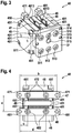
- Fig. 3 shows the mechanical structure of the rectifier 40 according to the present embodiment on a mounting receiving unit 51 of the device 50 in more detail.
- the assembly receiving unit 51 is the output to the welding electrode 11.
- Fig. 4 and Fig. 5 show various side views of the rectifier 40.
- the rectifier 40 has a first pressure plate 45, a second pressure plate 46, an A-side part 47, a B-side part 48 and a central part 49.
- Two semiconductor modules 401 are arranged between the A-side part 47 and the central part 49.
- Two semiconductor modules 401 are likewise arranged between the B-side part 48 and the middle part 49.
- Fig. 3 only the connection lugs of the semiconductor modules 401 for connection plug connectors 402 are visible.
- the function with pole switching or polarity switching can thus be implemented with the rectifier 40, as before on the basis of FIG Fig. 1 described. Without pole switching, there are only two modules 401, which will be discussed below with reference to FIG FIGS. 6 to 8 is described in more detail.
- the rectifier 40 has a sandwich construction in which the middle part 49 is arranged between the A-side part 47 and the B-side part 48.
- the combination of parts 47, 49, 48 is arranged between the A-side part 47 and the B-side part 48.
- the first pressure plate 45, the A-side part 47, the middle part 49, the B-side part 48 and the second pressure plate 46 are arranged one after the other or next to one another in the order mentioned.
- Said combination 45, 47, 49, 48, 46 is fastened to one another with fastening elements 451.
- the fasteners 451 are through the combination 45, 47, 49, 48, 46 pushed through. This is in Fig. 4 more visible.
- At least one of the fastening elements 451 can be a screw which is screwed into an invisible thread of the pressure plate 46.
- at least one of the fastening elements 451 can be a screw which is screwed into a nut received in the pressure plate 46.
- the side parts 47, 48 are designed as electrically conductive plates, in particular copper plates, etc. Of course, a different electrically conductive material, in particular metal, can be used for the side parts 47, 48.
- the side parts 47, 48 can also be referred to as transformer AC voltage copper plates.
- the middle part 49 is made of an electrically conductive material.
- the middle part 49 is conductively attached to the mounting support unit 51, in particular screwed, and is thus part of the current output in the direction of the welding electrode 11.
- the side parts 47, 48 which, as described above, consist of a conductive material, are attached to the mounting plate 51 in an insulated manner, especially screwed.
- the pressure plates 45, 46 are made of a conductive material.
- the pressure plates 45, 46 are isolated from the adjacent side parts 47, 48 by insulating disks 450.
- an insulating disk 450 is arranged between the side part 47 and the pressure plate 45.
- an insulating disk 450 for contactless assembly is provided between the side part 48 and the pressure plate 46, even if the insulating disk 450 is shown in FIG Fig. 3 is not visible.
- the side parts 47, 48 and the middle part 49 are fastened to the mounting receiving unit 51 by means of fastening elements 511 to 513.
- the side parts 47, 48 regardless of whether they are placed on the left or right or vice versa relative to the middle part 49, are fastened to the mounting receiving unit 51 by means of insulation, which is designed in particular as at least one insulation disk.
- the fasteners 511-513 are in the example of FIG Fig. 3 Screws that are fastened in openings in the side parts 47, 48, the middle part 49 and the mounting receiving unit 51.
- the fastening elements 511 and 513 require due to the required insulation between the side parts 47, 48 and the Mounting receiving unit 51 an additional insulating washer 450 for the contactless yet fixed mounting of the individual parts 47, 48, 49.
- the openings 514 are used to fasten further conductive plates, in particular copper plates, etc., which then form the expression of the connections of the finished transformer 30.
- the openings 514 may have an internal thread in the mounting receiving unit 51.
- the assembly receiving unit 51 has an opening 515 which can be used for cooling the rectifier 40.
- a liquid or gaseous medium in particular water, oil, or air, etc., can be used as the cooling medium.
- At least one fastening element 471 is provided on the A-side part 47, with which the transformer 30 can be fastened in a conductive manner to the rectifier 40, in particular can be screwed on by means of a screw.
- An opening 472 can be used for cooling the rectifier 40.
- a liquid or gaseous medium, in particular water, oil, or air, etc., can be used as the cooling medium.
- At least one fastening element 481 is provided on the B-side part 48, with which the transformer 30 can be fastened to the rectifier 40 in a conductive manner, in particular can be screwed on by means of a screw.
- An opening 482 can be used for cooling the rectifier 40.
- the transformer 30 can be fastened to the rectifier 40 at up to two fastening points with the aid of the fastening elements 471.
- the transformer 30 can be attached to up to two locations be fastened to the rectifier 40 with the aid of the fastening elements 481.
- the openings 472, 482 are spaced apart by the distances a, b, c, d, as in FIG Fig. 4 specified.
- One of the two openings 472, 482 forms the supply or inlet for the cooling medium into the rectifier 40.
- the other of the two openings 472, 482 forms the outlet for the cooling medium into the rectifier 40A.
- the fastening elements 511 to 514 are provided in the form of screws and / or rivets on the mounting plate 51 such that the side parts 47, 48 and the middle part 49 for both mounting variants of the side parts 47, 48 on one of the mounting receiving units 51, 52 are attachable.
- the other assembly variant is below with reference to FIGS. 6 to 8 described.
- an elongated hole solution as fastening elements 471, 481 and / or 511 to 513 in order to realize an assembly of the side parts 47, 48 for two different positions.
- two screw holes in the transformer 30 can be used.
- the fastening elements 511, 513 and the side parts 47, 48 have elongated holes as fastening openings, on the transformer 30 for the transformer variant of FIGS. 3 to 5 (with pole changing) and for the transformer variant of FIGS. 6 to 8 (without pole switching) the same fastening openings can still be used.
- FIGS. 6 to 8 show the structure of a rectifier 40A without pole switching or polarity switching.
- the rectifier 40A is constructed in many parts in the same way as described above with reference to the preceding exemplary embodiment with pole-changing for the rectifier 40.
- the rectifier 40A of FIGS. 6 to 8 the side parts 47, 48 are arranged reversed relative to the central part 49.
- the B-side panel is 48 in Fig. 6 now arranged on the left side of the middle part 49.
- only one semiconductor module 401 is arranged between the A side part 47 and the middle part 49.
- Fig. 7 only two connection lugs or direct plug connectors 4013 for semiconductor modules 401 for connection plug connectors 402 visible.
- the rectifier 40A the omission of two semiconductor modules 401 is forced only by interchanging the side parts 47, 48.
- the function can be implemented without pole switching or polarity switching, as already mentioned above in relation to the previous exemplary embodiment.
- two or four semiconductor modules pole switching or polarity switching
- two or four semiconductor modules can be used by interchanging the side parts 47, 48 and still using the same screw-on points on the transformer 30.
- the assembly receiving unit 51 of the rectifier 40 from FIG Fig. 2 is the output to welding electrode 11 in rectifier 40A of FIG Fig. 6 formed with a mounting receiving unit 52.
- the mounting receiving unit 52 of the rectifier 40A of FIG Fig. 6 is the only part that is different from the rectifier 40 of Fig. 2 differs.
- fastening elements 521 to 524 in the form of screws and / or rivets are provided on the mounting receiving unit 52.
- the mounting receiving unit 52 has an opening 525 which can be used for cooling the rectifier 40A.
- the side parts 47, 48 and the central part 49 are fastened to the mounting receiving unit 52 by means of fastening elements 521 to 523.
- the side parts 47, 48 regardless of whether they are placed on the left or right or vice versa relative to the middle part 49, are fastened to the assembly receiving unit 52 by means of insulation, which is designed in particular as at least one insulation disk 450.
- the fasteners 521-523 are in the example of FIG Fig. 2 Screws that go into Openings of the side parts 47, 48, the middle part 49 and the mounting receiving unit 52 are attached. Due to the required insulation between the side parts 47, 48 and the assembly receiving unit 52, the fastening elements 521 and 523 require an additional insulating washer 450 for the contactless yet firm assembly of the individual parts 47, 48, 49.
- the construction of the rectifier 40, 40A can be implemented very flexibly and inexpensively for the particular application required.
- the same transistors or semiconductor modules 401 in particular MOSFET modules, can be used for all transistors 41 to 44 by placing the plug connection or the connection plug connector 402 on the semiconductor modules 401.
- transformers 30 with pole changing and transformers 30 without pole changing with rectifiers 40, 40A with the same side parts 47, 48 can be realized.
- the same parts are used for rectifiers 40, 40A regardless of whether transformers 30 with pole changing and transformers 30 without pole changing are to be combined with rectifiers 40, 40A.
- transformers 30 with pole-changing and the transformers 30 without pole-changing can be controlled with the same driver board 403 (with assembly variants), as mentioned above.
- Fig. 9 shows a welding device 3 with a rectifier 400 according to a third embodiment.
- the welding device 3 is in particular a resistance welding device.
- the welding device 3 is constructed in many parts in the same way as described for the welding device 2 according to the preceding exemplary embodiment.
- the components 41, 42, 43, 44 which are designed as the modules 401 and thus as identical parts, have at least one transistor, but in particular up to approximately 50 transistors. However, the number is depending on the needs of the any welding application can be selected.
- the BODY diodes are shown in all components 41, 42, 43, 44.
- the transistors 41, 42, 43, 44 in the welding device 3 according to the present exemplary embodiment are each specially designed as metal-oxide-semiconductor field effect transistors (MOS-FETs).
- MOS-FETs metal-oxide-semiconductor field effect transistors
- the metal-oxide-semiconductor field effect transistors are connected in anti-parallel in the welding device 3.
- Fig. 9 shows the variant with pole changing. If the variant is to be implemented without pole switching, only the transistors 42, 44 are required in which the source connection S is connected to the transformer 30 and the drain connection is connected to the respective electrodes 11, 12.
- a primary voltage U1 results on the primary side of the welding transformer 30 from a bridge circuit 60 of semiconductor switches 61, 62, 63, 64.
- IGBT Insulated -Gate Bipolar Transistor
- the first semiconductor switch 61 and the second semiconductor switch 62 are connected in series.
- the third semiconductor switch 63 and the fourth semiconductor switch 64 are connected in series.
- the primary voltage U1 is formed on the primary side of the welding transformer 30 between a first connection node 71, which is arranged between the first and second semiconductor switches 61, 62, and a second connection node 72, which is arranged between the third and fourth semiconductor switches 63, 64 .
- a first secondary voltage U21 is applied to the secondary side of the welding transformer 30 between the first and second output 31, 32 of the welding transformer 30.
- a second secondary voltage U22 is applied between the second and third output 32, 33 of the welding transformer 30. After rectification by the rectifier 400, the first secondary voltage U21 and the second secondary voltage U22 form the welding voltage U23 in a preselected polarity
- the welding transformer 30 converts the primary voltage U1 into the first and second secondary voltages U21, U22.
- the sum of the secondary voltages U21, U22 is smaller than the value of the primary voltage U1.
- the welding transformer 30 converts a primary current I1 on the primary side of the welding transformer 30 into the secondary current I2 on the secondary side of the welding transformer 30.
- the secondary current l2, which can also be referred to as the welding current, has a higher value than the primary current l1.
- the welding device 3 can be used instead of the welding device 2 according to the preceding exemplary embodiment in the system 1 according to the preceding exemplary embodiment.
- the rectifier 400 can be configured in the same way as described in relation to the first and second exemplary embodiments.
- the welding device 3 can also be used particularly advantageously in sheet metal combinations in which the welding electrodes burn off at different rates in one welding gun.
- the welding device 3 can be used particularly advantageously when welding chain links and when welding radiators.
- two semiconductor modules 401 are arranged together between one of the side parts 47 and the middle part 49 and are connected as a series connection of two transistors 41, 42 between the welding tool 10 and an output 31 of the welding transformer 30 and two other semiconductor modules 401 are arranged together between the other of the side parts 48 and the middle part 49 and are connected as a series connection of two transistors or 43, 44 between the welding tool 10 and another output 33 of the welding transformer 30.
- This makes it possible to change the pole of the transformer 30, as described above with reference to the first exemplary embodiment. If no pole switching of the transformer 30 is required, the at least two semiconductor modules can each be arranged individually between one of the side parts 47, 48 and the central part 49 and connected between the welding tool 10 and an output of the welding transformer 30.
- the welding transformer 30 it is also possible for the welding transformer 30 to have at least two, but preferably three, outputs, with a series connection of two transistors 41, 42; 43, 44, the ends of the series connections are connected to one another and are connected to the preferably third output of the welding transformer 30 at or in front of the welding tool 10. It is also possible that the series connection of the transistors 41, 42; 43, 44 consists only of one or more transistors connected in parallel with the same polarity. It is also possible that for the variant without pole changing, as in relation to Fig. 6 and Fig. 7 described, at two of the outputs 31, 33 each consists of only one transistor.
- the transistors 41, 42, 43, 44 can alternatively be bipolar transistors, although the embodiment as metal-oxide-semiconductor field effect transistors (MOS-FET) is preferred.
- MOS-FET metal-oxide-semiconductor field effect transistors
- the welding transformer 30 can be constructed from a parallel connection of two transformers.
- Up to four semiconductor modules 401 are possibly provided between a side part 47, 48 and the middle part 49. It goes without saying that the number of semiconductor modules 401 can be greater depending on requirements and configuration. In addition, for special applications 3 or 5 or more semiconductor modules 401 can be arranged between a side part 47, 48 and the central part 49.
- the system 1 may have a hand tool instead of the welding tool 10 guided by the device 50.
- the device 50 can alternatively be configured such that the welding tool 10 is a hand-held tool.
- the system 1 has at least one further tool, such as a screwing, drilling or milling tool, or riveting tool or cutting tool or Tox tool or punching tool.
Landscapes
- Engineering & Computer Science (AREA)
- Power Engineering (AREA)
- Mechanical Engineering (AREA)
- Rectifiers (AREA)
- Generation Of Surge Voltage And Current (AREA)
- Dc-Dc Converters (AREA)
- Lining Or Joining Of Plastics Or The Like (AREA)
Applications Claiming Priority (1)
| Application Number | Priority Date | Filing Date | Title |
|---|---|---|---|
| DE102019204794.7A DE102019204794A1 (de) | 2019-04-04 | 2019-04-04 | Gleichrichter für einen Schweißtransformator einer Schweißvorrichtung und Verfahren zum Herstellen eines solchen Gleichrichters |
Publications (3)
| Publication Number | Publication Date |
|---|---|
| EP3718672A2 true EP3718672A2 (fr) | 2020-10-07 |
| EP3718672A3 EP3718672A3 (fr) | 2020-11-04 |
| EP3718672B1 EP3718672B1 (fr) | 2023-08-09 |
Family
ID=69770421
Family Applications (1)
| Application Number | Title | Priority Date | Filing Date |
|---|---|---|---|
| EP20160577.1A Active EP3718672B1 (fr) | 2019-04-04 | 2020-03-03 | Redresseur pour un transformateur de soudage d'un dispositif de soudage et procédé de fabrication d'un tel redresseur |
Country Status (4)
| Country | Link |
|---|---|
| EP (1) | EP3718672B1 (fr) |
| CN (1) | CN111800021B (fr) |
| DE (1) | DE102019204794A1 (fr) |
| ES (1) | ES2962831T3 (fr) |
Families Citing this family (1)
| Publication number | Priority date | Publication date | Assignee | Title |
|---|---|---|---|---|
| CN113690035B (zh) * | 2021-08-20 | 2023-08-11 | 中正智控(江苏)智能科技有限公司 | 一种具有改变极性功能的次高频直流电阻焊焊接变压器 |
Family Cites Families (5)
| Publication number | Priority date | Publication date | Assignee | Title |
|---|---|---|---|---|
| JPH04253579A (ja) * | 1991-02-01 | 1992-09-09 | Honda Motor Co Ltd | 直流抵抗溶接装置 |
| US9956639B2 (en) * | 2005-02-07 | 2018-05-01 | Lincoln Global, Inc | Modular power source for electric ARC welding and output chopper |
| DE102011121836A1 (de) * | 2011-12-21 | 2013-06-27 | Robert Bosch Gmbh | Verfahren zum Betrieb einer Widerstandsschweißvorrichtung |
| CN203936512U (zh) * | 2014-04-30 | 2014-11-12 | 锦州市圣合科技电子有限责任公司 | 电阻焊机用中频大功率组件 |
| CN105817740B (zh) * | 2016-05-03 | 2018-05-01 | 深圳市佳士科技股份有限公司 | 焊接电源及交直流氩弧焊机 |
-
2019
- 2019-04-04 DE DE102019204794.7A patent/DE102019204794A1/de active Pending
-
2020
- 2020-03-03 EP EP20160577.1A patent/EP3718672B1/fr active Active
- 2020-03-03 ES ES20160577T patent/ES2962831T3/es active Active
- 2020-04-03 CN CN202010259774.1A patent/CN111800021B/zh active Active
Also Published As
| Publication number | Publication date |
|---|---|
| CN111800021B (zh) | 2025-07-01 |
| DE102019204794A1 (de) | 2020-10-08 |
| EP3718672A3 (fr) | 2020-11-04 |
| CN111800021A (zh) | 2020-10-20 |
| ES2962831T3 (es) | 2024-03-21 |
| EP3718672B1 (fr) | 2023-08-09 |
Similar Documents
| Publication | Publication Date | Title |
|---|---|---|
| DE4110339C2 (de) | Wechselrichter mit plattenförmigen Gleichspannungszuleitungen | |
| DE102015101086B4 (de) | Leistungshalbleitermodulanordnung | |
| DE19732402B4 (de) | Elektrische Busanordnung zur Gleichstromversorgung von Schaltungselementen eines Wechselrichters | |
| EP3000168B1 (fr) | Convertisseur electronique a plusieur niveaux | |
| DE69427629T2 (de) | Halbleiterstapel | |
| EP2302782A1 (fr) | Agencement de convertisseur de courant | |
| EP3404818B1 (fr) | Dispositif de semi-conducteurs | |
| EP3557614A1 (fr) | Module de puissance pourvu d'un composant électronique de puissance sur une plaque de substrat et circuit électronique de puissance pourvu d'un tel module de puissance | |
| AT512069B1 (de) | Widerstandsschweissvorrichtung | |
| EP2959492B1 (fr) | Procédé pour faire fonctionner un changeur de prises en charge avec des éléments de commutation à semi-conducteurs | |
| DE4005333A1 (de) | Elektronischer leistungs-schalter | |
| DE102016205206B4 (de) | Elektronische Steuereinheit | |
| EP3718672B1 (fr) | Redresseur pour un transformateur de soudage d'un dispositif de soudage et procédé de fabrication d'un tel redresseur | |
| EP3718673B1 (fr) | Redresseur pour un transformateur de soudage d'un dispositif de soudage et procédé de fabrication d'un tel redresseur | |
| EP3584029A1 (fr) | Dispositif de soudage par résistance et procédé de soudage par résistance permettant de souder par résistance au moins un composant | |
| EP3722041A2 (fr) | Dispositif de soudage par résistance et procédé de soudage par résistance permettant de souder par résistance au moins un composant | |
| DE2218612A1 (de) | Gleichrichteranordnung mit gekühlter Stromzuführung | |
| DE102015225038A1 (de) | Widerstandsschweissvorrichtung und Widerstandsschweissverfahren zum Widerstandsschweissen von mindestens einem Bauteil | |
| EP3181284B1 (fr) | Circuit de convertisseur | |
| DE202013105809U1 (de) | Leistungshalbleitermodul und Kontaktierungsanordnung | |
| DE102014107271B4 (de) | Halbleitermodul | |
| DE102015213916B4 (de) | Leistungshalbleitermodulanordnung | |
| DE102006038541B4 (de) | Halbleiterbauelementanordnung mit komplementären Leistungsbauelementen | |
| DE10114323A1 (de) | Vorrichtung zum Widerstandsschweißen | |
| DE102022207268A1 (de) | Inverteranordnung |
Legal Events
| Date | Code | Title | Description |
|---|---|---|---|
| PUAI | Public reference made under article 153(3) epc to a published international application that has entered the european phase |
Free format text: ORIGINAL CODE: 0009012 |
|
| STAA | Information on the status of an ep patent application or granted ep patent |
Free format text: STATUS: THE APPLICATION HAS BEEN PUBLISHED |
|
| PUAL | Search report despatched |
Free format text: ORIGINAL CODE: 0009013 |
|
| AK | Designated contracting states |
Kind code of ref document: A2 Designated state(s): AL AT BE BG CH CY CZ DE DK EE ES FI FR GB GR HR HU IE IS IT LI LT LU LV MC MK MT NL NO PL PT RO RS SE SI SK SM TR |
|
| AX | Request for extension of the european patent |
Extension state: BA ME |
|
| AK | Designated contracting states |
Kind code of ref document: A3 Designated state(s): AL AT BE BG CH CY CZ DE DK EE ES FI FR GB GR HR HU IE IS IT LI LT LU LV MC MK MT NL NO PL PT RO RS SE SI SK SM TR |
|
| AX | Request for extension of the european patent |
Extension state: BA ME |
|
| RIC1 | Information provided on ipc code assigned before grant |
Ipc: B23K 11/24 20060101AFI20200928BHEP Ipc: H02M 7/00 20060101ALI20200928BHEP |
|
| STAA | Information on the status of an ep patent application or granted ep patent |
Free format text: STATUS: REQUEST FOR EXAMINATION WAS MADE |
|
| 17P | Request for examination filed |
Effective date: 20210504 |
|
| RBV | Designated contracting states (corrected) |
Designated state(s): AL AT BE BG CH CY CZ DE DK EE ES FI FR GB GR HR HU IE IS IT LI LT LU LV MC MK MT NL NO PL PT RO RS SE SI SK SM TR |
|
| GRAP | Despatch of communication of intention to grant a patent |
Free format text: ORIGINAL CODE: EPIDOSNIGR1 |
|
| STAA | Information on the status of an ep patent application or granted ep patent |
Free format text: STATUS: GRANT OF PATENT IS INTENDED |
|
| RIC1 | Information provided on ipc code assigned before grant |
Ipc: H02M 7/00 20060101ALI20230421BHEP Ipc: B23K 11/24 20060101AFI20230421BHEP |
|
| INTG | Intention to grant announced |
Effective date: 20230525 |
|
| GRAS | Grant fee paid |
Free format text: ORIGINAL CODE: EPIDOSNIGR3 |
|
| GRAA | (expected) grant |
Free format text: ORIGINAL CODE: 0009210 |
|
| STAA | Information on the status of an ep patent application or granted ep patent |
Free format text: STATUS: THE PATENT HAS BEEN GRANTED |
|
| AK | Designated contracting states |
Kind code of ref document: B1 Designated state(s): AL AT BE BG CH CY CZ DE DK EE ES FI FR GB GR HR HU IE IS IT LI LT LU LV MC MK MT NL NO PL PT RO RS SE SI SK SM TR |
|
| REG | Reference to a national code |
Ref country code: GB Ref legal event code: FG4D Free format text: NOT ENGLISH |
|
| REG | Reference to a national code |
Ref country code: CH Ref legal event code: EP |
|
| REG | Reference to a national code |
Ref country code: IE Ref legal event code: FG4D Free format text: LANGUAGE OF EP DOCUMENT: GERMAN |
|
| REG | Reference to a national code |
Ref country code: DE Ref legal event code: R096 Ref document number: 502020004566 Country of ref document: DE |
|
| REG | Reference to a national code |
Ref country code: LT Ref legal event code: MG9D |
|
| REG | Reference to a national code |
Ref country code: NL Ref legal event code: MP Effective date: 20230809 |
|
| PG25 | Lapsed in a contracting state [announced via postgrant information from national office to epo] |
Ref country code: GR Free format text: LAPSE BECAUSE OF FAILURE TO SUBMIT A TRANSLATION OF THE DESCRIPTION OR TO PAY THE FEE WITHIN THE PRESCRIBED TIME-LIMIT Effective date: 20231110 |
|
| PG25 | Lapsed in a contracting state [announced via postgrant information from national office to epo] |
Ref country code: IS Free format text: LAPSE BECAUSE OF FAILURE TO SUBMIT A TRANSLATION OF THE DESCRIPTION OR TO PAY THE FEE WITHIN THE PRESCRIBED TIME-LIMIT Effective date: 20231209 |
|
| PG25 | Lapsed in a contracting state [announced via postgrant information from national office to epo] |
Ref country code: SE Free format text: LAPSE BECAUSE OF FAILURE TO SUBMIT A TRANSLATION OF THE DESCRIPTION OR TO PAY THE FEE WITHIN THE PRESCRIBED TIME-LIMIT Effective date: 20230809 Ref country code: RS Free format text: LAPSE BECAUSE OF FAILURE TO SUBMIT A TRANSLATION OF THE DESCRIPTION OR TO PAY THE FEE WITHIN THE PRESCRIBED TIME-LIMIT Effective date: 20230809 Ref country code: PT Free format text: LAPSE BECAUSE OF FAILURE TO SUBMIT A TRANSLATION OF THE DESCRIPTION OR TO PAY THE FEE WITHIN THE PRESCRIBED TIME-LIMIT Effective date: 20231211 Ref country code: NO Free format text: LAPSE BECAUSE OF FAILURE TO SUBMIT A TRANSLATION OF THE DESCRIPTION OR TO PAY THE FEE WITHIN THE PRESCRIBED TIME-LIMIT Effective date: 20231109 Ref country code: NL Free format text: LAPSE BECAUSE OF FAILURE TO SUBMIT A TRANSLATION OF THE DESCRIPTION OR TO PAY THE FEE WITHIN THE PRESCRIBED TIME-LIMIT Effective date: 20230809 Ref country code: LV Free format text: LAPSE BECAUSE OF FAILURE TO SUBMIT A TRANSLATION OF THE DESCRIPTION OR TO PAY THE FEE WITHIN THE PRESCRIBED TIME-LIMIT Effective date: 20230809 Ref country code: LT Free format text: LAPSE BECAUSE OF FAILURE TO SUBMIT A TRANSLATION OF THE DESCRIPTION OR TO PAY THE FEE WITHIN THE PRESCRIBED TIME-LIMIT Effective date: 20230809 Ref country code: IS Free format text: LAPSE BECAUSE OF FAILURE TO SUBMIT A TRANSLATION OF THE DESCRIPTION OR TO PAY THE FEE WITHIN THE PRESCRIBED TIME-LIMIT Effective date: 20231209 Ref country code: HR Free format text: LAPSE BECAUSE OF FAILURE TO SUBMIT A TRANSLATION OF THE DESCRIPTION OR TO PAY THE FEE WITHIN THE PRESCRIBED TIME-LIMIT Effective date: 20230809 Ref country code: GR Free format text: LAPSE BECAUSE OF FAILURE TO SUBMIT A TRANSLATION OF THE DESCRIPTION OR TO PAY THE FEE WITHIN THE PRESCRIBED TIME-LIMIT Effective date: 20231110 Ref country code: FI Free format text: LAPSE BECAUSE OF FAILURE TO SUBMIT A TRANSLATION OF THE DESCRIPTION OR TO PAY THE FEE WITHIN THE PRESCRIBED TIME-LIMIT Effective date: 20230809 |
|
| PG25 | Lapsed in a contracting state [announced via postgrant information from national office to epo] |
Ref country code: PL Free format text: LAPSE BECAUSE OF FAILURE TO SUBMIT A TRANSLATION OF THE DESCRIPTION OR TO PAY THE FEE WITHIN THE PRESCRIBED TIME-LIMIT Effective date: 20230809 |
|
| REG | Reference to a national code |
Ref country code: ES Ref legal event code: FG2A Ref document number: 2962831 Country of ref document: ES Kind code of ref document: T3 Effective date: 20240321 |
|
| PG25 | Lapsed in a contracting state [announced via postgrant information from national office to epo] |
Ref country code: SM Free format text: LAPSE BECAUSE OF FAILURE TO SUBMIT A TRANSLATION OF THE DESCRIPTION OR TO PAY THE FEE WITHIN THE PRESCRIBED TIME-LIMIT Effective date: 20230809 Ref country code: RO Free format text: LAPSE BECAUSE OF FAILURE TO SUBMIT A TRANSLATION OF THE DESCRIPTION OR TO PAY THE FEE WITHIN THE PRESCRIBED TIME-LIMIT Effective date: 20230809 Ref country code: EE Free format text: LAPSE BECAUSE OF FAILURE TO SUBMIT A TRANSLATION OF THE DESCRIPTION OR TO PAY THE FEE WITHIN THE PRESCRIBED TIME-LIMIT Effective date: 20230809 Ref country code: DK Free format text: LAPSE BECAUSE OF FAILURE TO SUBMIT A TRANSLATION OF THE DESCRIPTION OR TO PAY THE FEE WITHIN THE PRESCRIBED TIME-LIMIT Effective date: 20230809 Ref country code: CZ Free format text: LAPSE BECAUSE OF FAILURE TO SUBMIT A TRANSLATION OF THE DESCRIPTION OR TO PAY THE FEE WITHIN THE PRESCRIBED TIME-LIMIT Effective date: 20230809 Ref country code: SK Free format text: LAPSE BECAUSE OF FAILURE TO SUBMIT A TRANSLATION OF THE DESCRIPTION OR TO PAY THE FEE WITHIN THE PRESCRIBED TIME-LIMIT Effective date: 20230809 |
|
| REG | Reference to a national code |
Ref country code: DE Ref legal event code: R097 Ref document number: 502020004566 Country of ref document: DE |
|
| PG25 | Lapsed in a contracting state [announced via postgrant information from national office to epo] |
Ref country code: IT Free format text: LAPSE BECAUSE OF FAILURE TO SUBMIT A TRANSLATION OF THE DESCRIPTION OR TO PAY THE FEE WITHIN THE PRESCRIBED TIME-LIMIT Effective date: 20230809 |
|
| PLBE | No opposition filed within time limit |
Free format text: ORIGINAL CODE: 0009261 |
|
| STAA | Information on the status of an ep patent application or granted ep patent |
Free format text: STATUS: NO OPPOSITION FILED WITHIN TIME LIMIT |
|
| 26N | No opposition filed |
Effective date: 20240513 |
|
| PG25 | Lapsed in a contracting state [announced via postgrant information from national office to epo] |
Ref country code: SI Free format text: LAPSE BECAUSE OF FAILURE TO SUBMIT A TRANSLATION OF THE DESCRIPTION OR TO PAY THE FEE WITHIN THE PRESCRIBED TIME-LIMIT Effective date: 20230809 |
|
| REG | Reference to a national code |
Ref country code: CH Ref legal event code: PL |
|
| PG25 | Lapsed in a contracting state [announced via postgrant information from national office to epo] |
Ref country code: BG Free format text: LAPSE BECAUSE OF FAILURE TO SUBMIT A TRANSLATION OF THE DESCRIPTION OR TO PAY THE FEE WITHIN THE PRESCRIBED TIME-LIMIT Effective date: 20230809 |
|
| PG25 | Lapsed in a contracting state [announced via postgrant information from national office to epo] |
Ref country code: LU Free format text: LAPSE BECAUSE OF NON-PAYMENT OF DUE FEES Effective date: 20240303 |
|
| PG25 | Lapsed in a contracting state [announced via postgrant information from national office to epo] |
Ref country code: MC Free format text: LAPSE BECAUSE OF FAILURE TO SUBMIT A TRANSLATION OF THE DESCRIPTION OR TO PAY THE FEE WITHIN THE PRESCRIBED TIME-LIMIT Effective date: 20230809 |
|
| GBPC | Gb: european patent ceased through non-payment of renewal fee |
Effective date: 20240303 |
|
| PG25 | Lapsed in a contracting state [announced via postgrant information from national office to epo] |
Ref country code: MC Free format text: LAPSE BECAUSE OF FAILURE TO SUBMIT A TRANSLATION OF THE DESCRIPTION OR TO PAY THE FEE WITHIN THE PRESCRIBED TIME-LIMIT Effective date: 20230809 Ref country code: LU Free format text: LAPSE BECAUSE OF NON-PAYMENT OF DUE FEES Effective date: 20240303 Ref country code: BG Free format text: LAPSE BECAUSE OF FAILURE TO SUBMIT A TRANSLATION OF THE DESCRIPTION OR TO PAY THE FEE WITHIN THE PRESCRIBED TIME-LIMIT Effective date: 20230809 |
|
| REG | Reference to a national code |
Ref country code: BE Ref legal event code: MM Effective date: 20240331 |
|
| PG25 | Lapsed in a contracting state [announced via postgrant information from national office to epo] |
Ref country code: BE Free format text: LAPSE BECAUSE OF NON-PAYMENT OF DUE FEES Effective date: 20240331 |
|
| PG25 | Lapsed in a contracting state [announced via postgrant information from national office to epo] |
Ref country code: GB Free format text: LAPSE BECAUSE OF NON-PAYMENT OF DUE FEES Effective date: 20240303 |
|
| PG25 | Lapsed in a contracting state [announced via postgrant information from national office to epo] |
Ref country code: IE Free format text: LAPSE BECAUSE OF NON-PAYMENT OF DUE FEES Effective date: 20240303 |
|
| PG25 | Lapsed in a contracting state [announced via postgrant information from national office to epo] |
Ref country code: IE Free format text: LAPSE BECAUSE OF NON-PAYMENT OF DUE FEES Effective date: 20240303 Ref country code: GB Free format text: LAPSE BECAUSE OF NON-PAYMENT OF DUE FEES Effective date: 20240303 Ref country code: BE Free format text: LAPSE BECAUSE OF NON-PAYMENT OF DUE FEES Effective date: 20240331 Ref country code: CH Free format text: LAPSE BECAUSE OF NON-PAYMENT OF DUE FEES Effective date: 20240331 |
|
| PGFP | Annual fee paid to national office [announced via postgrant information from national office to epo] |
Ref country code: AT Payment date: 20250417 Year of fee payment: 5 |
|
| PGFP | Annual fee paid to national office [announced via postgrant information from national office to epo] |
Ref country code: DE Payment date: 20250522 Year of fee payment: 6 |
|
| PGFP | Annual fee paid to national office [announced via postgrant information from national office to epo] |
Ref country code: ES Payment date: 20250416 Year of fee payment: 6 |
|
| PG25 | Lapsed in a contracting state [announced via postgrant information from national office to epo] |
Ref country code: CY Free format text: LAPSE BECAUSE OF FAILURE TO SUBMIT A TRANSLATION OF THE DESCRIPTION OR TO PAY THE FEE WITHIN THE PRESCRIBED TIME-LIMIT; INVALID AB INITIO Effective date: 20200303 |
|
| PG25 | Lapsed in a contracting state [announced via postgrant information from national office to epo] |
Ref country code: HU Free format text: LAPSE BECAUSE OF FAILURE TO SUBMIT A TRANSLATION OF THE DESCRIPTION OR TO PAY THE FEE WITHIN THE PRESCRIBED TIME-LIMIT; INVALID AB INITIO Effective date: 20200303 |
|
| PG25 | Lapsed in a contracting state [announced via postgrant information from national office to epo] |
Ref country code: TR Free format text: LAPSE BECAUSE OF FAILURE TO SUBMIT A TRANSLATION OF THE DESCRIPTION OR TO PAY THE FEE WITHIN THE PRESCRIBED TIME-LIMIT Effective date: 20230809 |
|
| PGFP | Annual fee paid to national office [announced via postgrant information from national office to epo] |
Ref country code: FR Payment date: 20260325 Year of fee payment: 7 |