EP3719783B1 - Schieberegister, ansteuerungsverfahren dafür, gatetreiberschaltung und anzeigevorrichtung - Google Patents
Schieberegister, ansteuerungsverfahren dafür, gatetreiberschaltung und anzeigevorrichtung Download PDFInfo
- Publication number
- EP3719783B1 EP3719783B1 EP18855161.8A EP18855161A EP3719783B1 EP 3719783 B1 EP3719783 B1 EP 3719783B1 EP 18855161 A EP18855161 A EP 18855161A EP 3719783 B1 EP3719783 B1 EP 3719783B1
- Authority
- EP
- European Patent Office
- Prior art keywords
- terminal
- pull
- node
- output
- shift register
- Prior art date
- Legal status (The legal status is an assumption and is not a legal conclusion. Google has not performed a legal analysis and makes no representation as to the accuracy of the status listed.)
- Active
Links
Images



Classifications
-
- G—PHYSICS
- G09—EDUCATION; CRYPTOGRAPHY; DISPLAY; ADVERTISING; SEALS
- G09G—ARRANGEMENTS OR CIRCUITS FOR CONTROL OF INDICATING DEVICES USING STATIC MEANS TO PRESENT VARIABLE INFORMATION
- G09G3/00—Control arrangements or circuits, of interest only in connection with visual indicators other than cathode-ray tubes
- G09G3/20—Control arrangements or circuits, of interest only in connection with visual indicators other than cathode-ray tubes for presentation of an assembly of a number of characters, e.g. a page, by composing the assembly by combination of individual elements arranged in a matrix no fixed position being assigned to or needed to be assigned to the individual characters or partial characters
- G09G3/34—Control arrangements or circuits, of interest only in connection with visual indicators other than cathode-ray tubes for presentation of an assembly of a number of characters, e.g. a page, by composing the assembly by combination of individual elements arranged in a matrix no fixed position being assigned to or needed to be assigned to the individual characters or partial characters by control of light from an independent source
- G09G3/36—Control arrangements or circuits, of interest only in connection with visual indicators other than cathode-ray tubes for presentation of an assembly of a number of characters, e.g. a page, by composing the assembly by combination of individual elements arranged in a matrix no fixed position being assigned to or needed to be assigned to the individual characters or partial characters by control of light from an independent source using liquid crystals
- G09G3/3611—Control of matrices with row and column drivers
- G09G3/3674—Details of drivers for scan electrodes
- G09G3/3677—Details of drivers for scan electrodes suitable for active matrices only
-
- G—PHYSICS
- G09—EDUCATION; CRYPTOGRAPHY; DISPLAY; ADVERTISING; SEALS
- G09G—ARRANGEMENTS OR CIRCUITS FOR CONTROL OF INDICATING DEVICES USING STATIC MEANS TO PRESENT VARIABLE INFORMATION
- G09G3/00—Control arrangements or circuits, of interest only in connection with visual indicators other than cathode-ray tubes
- G09G3/20—Control arrangements or circuits, of interest only in connection with visual indicators other than cathode-ray tubes for presentation of an assembly of a number of characters, e.g. a page, by composing the assembly by combination of individual elements arranged in a matrix no fixed position being assigned to or needed to be assigned to the individual characters or partial characters
- G09G3/2092—Details of a display terminals using a flat panel, the details relating to the control arrangement of the display terminal and to the interfaces thereto
-
- G—PHYSICS
- G11—INFORMATION STORAGE
- G11C—STATIC STORES
- G11C19/00—Digital stores in which the information is moved stepwise, e.g. shift registers
- G11C19/28—Digital stores in which the information is moved stepwise, e.g. shift registers using semiconductor elements
-
- G—PHYSICS
- G09—EDUCATION; CRYPTOGRAPHY; DISPLAY; ADVERTISING; SEALS
- G09G—ARRANGEMENTS OR CIRCUITS FOR CONTROL OF INDICATING DEVICES USING STATIC MEANS TO PRESENT VARIABLE INFORMATION
- G09G2310/00—Command of the display device
- G09G2310/02—Addressing, scanning or driving the display screen or processing steps related thereto
- G09G2310/0264—Details of driving circuits
- G09G2310/0267—Details of drivers for scan electrodes, other than drivers for liquid crystal, plasma or OLED displays
-
- G—PHYSICS
- G09—EDUCATION; CRYPTOGRAPHY; DISPLAY; ADVERTISING; SEALS
- G09G—ARRANGEMENTS OR CIRCUITS FOR CONTROL OF INDICATING DEVICES USING STATIC MEANS TO PRESENT VARIABLE INFORMATION
- G09G2310/00—Command of the display device
- G09G2310/02—Addressing, scanning or driving the display screen or processing steps related thereto
- G09G2310/0264—Details of driving circuits
- G09G2310/0283—Arrangement of drivers for different directions of scanning
-
- G—PHYSICS
- G09—EDUCATION; CRYPTOGRAPHY; DISPLAY; ADVERTISING; SEALS
- G09G—ARRANGEMENTS OR CIRCUITS FOR CONTROL OF INDICATING DEVICES USING STATIC MEANS TO PRESENT VARIABLE INFORMATION
- G09G2310/00—Command of the display device
- G09G2310/02—Addressing, scanning or driving the display screen or processing steps related thereto
- G09G2310/0264—Details of driving circuits
- G09G2310/0286—Details of a shift registers arranged for use in a driving circuit
-
- G—PHYSICS
- G09—EDUCATION; CRYPTOGRAPHY; DISPLAY; ADVERTISING; SEALS
- G09G—ARRANGEMENTS OR CIRCUITS FOR CONTROL OF INDICATING DEVICES USING STATIC MEANS TO PRESENT VARIABLE INFORMATION
- G09G3/00—Control arrangements or circuits, of interest only in connection with visual indicators other than cathode-ray tubes
- G09G3/20—Control arrangements or circuits, of interest only in connection with visual indicators other than cathode-ray tubes for presentation of an assembly of a number of characters, e.g. a page, by composing the assembly by combination of individual elements arranged in a matrix no fixed position being assigned to or needed to be assigned to the individual characters or partial characters
- G09G3/22—Control arrangements or circuits, of interest only in connection with visual indicators other than cathode-ray tubes for presentation of an assembly of a number of characters, e.g. a page, by composing the assembly by combination of individual elements arranged in a matrix no fixed position being assigned to or needed to be assigned to the individual characters or partial characters using controlled light sources
- G09G3/30—Control arrangements or circuits, of interest only in connection with visual indicators other than cathode-ray tubes for presentation of an assembly of a number of characters, e.g. a page, by composing the assembly by combination of individual elements arranged in a matrix no fixed position being assigned to or needed to be assigned to the individual characters or partial characters using controlled light sources using electroluminescent panels
- G09G3/32—Control arrangements or circuits, of interest only in connection with visual indicators other than cathode-ray tubes for presentation of an assembly of a number of characters, e.g. a page, by composing the assembly by combination of individual elements arranged in a matrix no fixed position being assigned to or needed to be assigned to the individual characters or partial characters using controlled light sources using electroluminescent panels semiconductive, e.g. using light-emitting diodes [LED]
- G09G3/3208—Control arrangements or circuits, of interest only in connection with visual indicators other than cathode-ray tubes for presentation of an assembly of a number of characters, e.g. a page, by composing the assembly by combination of individual elements arranged in a matrix no fixed position being assigned to or needed to be assigned to the individual characters or partial characters using controlled light sources using electroluminescent panels semiconductive, e.g. using light-emitting diodes [LED] organic, e.g. using organic light-emitting diodes [OLED]
- G09G3/3266—Details of drivers for scan electrodes
Definitions
- the present invention relates to the field of display technique, and more particularly, to a shift register, a gate driving circuit and a display device.
- CN 106 652 964 A discloses a shift register unit, a driving method thereof, a gate drive circuit and a display device.
- the shift register unit comprises an input module and a plurality of output modules coupled to the input module.
- the input module is coupled to an input signal end and is configured to operate the plurality of output modules under the control of the voltage at the input signal end.
- Each output module is coupled with a corresponding clock signal end and an output signal end and is configured to couple the clock signal end to the output signal end at work so as to output a drive signal at the output signal end.
- each shift-register stage has two output terminals and two pull-down circuits, each of the pull-down circuits can only drive one of the outputs, unlike the present disclosure.
- the pull-down control circuit which controls the multiple pull-down circuits differs in structure from the pull-down node selection circuit of this disclosure.
- the term "operating potential” refers to a potential capable of turning on a corresponding switching element or capable of enabling a corresponding circuit to operate. For example, if the switching element needs to be turned on when the potential at its control terminal is a high level, the operating potential may correspond to a high level, and if the switching element needs to be turned on when the potential at its control terminal is a low level, the operating potential may correspond to a low potential.
- reset potential refers to a potential opposite to the "operating potential", that is, a potential capable of turning off a corresponding switching element or enabling a corresponding circuit not to operate.
- the reset potential may correspond to a low level; or, if the operating potential corresponds to a low level, the reset potential may correspond to a high level.
- the operating potential and the reset potential may be determined according to the actual circuit conditions. In the following description, for the sake of brevity, a high level is selected as the operating potential, and a low level is selected as the reset potential. However, the technical solution of the present disclosure is not limited to such example.
- the potential at the terminal is a high level, or the terminal is at a high level.
- the potential at the terminal is a low level, or the terminal is at a low level.
- the high level and the low level are relative.
- a voltage value or voltage range of the low level may be selected according to the actual circuit conditions and the design standard, so that when the voltage is the selected value or within the selected range, the corresponding switching element is turned off or the corresponding circuit does not operate.
- the voltage value of the high level is usually higher than that of the low level.
- a voltage value or voltage range of the high level may be selected according to the actual circuit conditions and the design standard, so that when the voltage is the selected value or within the selected range, the corresponding switching element can be turned on or the corresponding circuit can operate.
- both the high and low levels may correspond to different voltage values within a certain range.
- terms like “first high level” and “second high level” may be used to describe high levels having different voltage values within a high level range.
- the switching element may be any element or circuit having a control terminal and capable of functioning as a switch.
- Such switching element can be turned on, for example, when the potential at its control terminal is a high level, that is, a path is formed between its first terminal and its second terminal, such that the potentials at its first terminal and its second terminal are the same or substantially the same.
- the switching element when the switching element is turned on, the potentials at its first terminal and its second terminal are not necessarily identical due to turn-on resistance of the switching element, there may be some difference.
- such switching element may employ various types of switching device having a control terminal such as a thin film transistor or a field effect transistor as needed, and may adopt an N-channel type or a P-channel type as needed.
- a control terminal such as a thin film transistor or a field effect transistor
- the switching element of an N-channel type thin film transistor may correspond to the gate of the transistor
- one of the first terminal and the second terminal of the transistor may correspond to one of the source and the drain of the transistor
- the other one of the first terminal and the second terminal of the transistor may correspond to the other one of the source and the drain of the transistor.
- the first terminal and the second terminal of the switch are interchangeable.
- the technical solution of the present disclosure is not limited to such example.
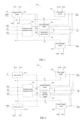
- FIG. 1 illustrates an exemplary shift register 100 according to an embodiment of the present disclosure.
- the shift register 100 comprises an input and reset circuit 101, a first output circuit 102, a second output circuit 103, a first pull-down circuit 104, a second pull-down circuit 105 and a pull-down node selection circuit 106.
- the shift register 100 further comprises a first pull-down node PD1 and a second pull-down node PD2.
- the input and reset circuit 101 is connected to an input terminal, a pull-up node and a reset terminal, and is configured in entirety to set the potential at the pull-up node to an operating potential when the potential at the input terminal is the operating potential, and set the potential at the pull-up node to a reset potential when the potential at the reset terminal is the operating potential.
- the input and reset circuit 101 illustrated in FIG. 1 may include an input circuit 101_1 and a reset circuit 101_2 as illustrated in FIG. 2 . It should be understood that the shift registers illustrated in FIGS. 1 and 2 differ in that the input and reset circuit in FIG. 1 is split into an input circuit 101_1 and a reset circuit 101_2 as illustrated in FIG. 2 .
- the input circuit 101_1 is connected to an input terminal IN of the shift register 100, a first scanning direction control terminal CN and a pull-up node PU.
- the input circuit 101_1 can, by turning on its internal switching element, enable the pull-up node PU to be connected to the input terminal IN and/or the first scanning direction control terminal CN, thereby causing the potential at the pull-up node PU to become an operating potential, such as a high level.
- the input circuit 101_1 may be implemented in different ways, and may be connected to different terminals of the shift register 100 according to needs and implementations, so that when an input signal is received via the input terminal IN, the potential at the pull-up node PU is set to the operating potential.
- the input circuit 101_1 may also be connected to an operating potential terminal VGH, wherein when a signal is received via the input terminal IN, the input circuit 101_1 may, by turning on its internal switching element, enable the pull-up node PU and the operating potential terminal VGH to be connected, thereby causing the potential at the pull-up node PU to become the operating potential.
- the input circuit 101_1 may also be connected to a clock signal terminal, and the clock signal terminal provides a high-level clock signal when a signal is received via the input terminal IN, wherein when a signal is received via the input terminal IN, the input circuit 101_1 can, by turning on its internal switching element, enable the pull-up node PU to be connected to the clock signal terminal, thereby causing the potential at the pull-up node PU to become the operating potential.
- the input circuit 101_1 may include at least one switching element, and for example, the control terminal of the switching element may be connected to the input terminal IN, one of the first terminal and the second terminal thereof may be connected to the pull-up node PU, and according to the situation the other one of the first terminal and the second terminal thereof is connected to the first scanning direction control terminal CN or the operating potential terminal VGH or the clock signal terminal as mentioned above.
- the input circuit 101_1 is also connected to the first pull-down node PD1 and a reference signal terminal RS. While the pull-up node PU is set to a high level, the input circuit 101_1 can, for example by turning on the internal switching element, enable the reference signal terminal RS and the first pull-down node PD1 to be connected, thereby setting the first pull-down node PD1 to a low level.
- the input circuit 101_1 may not be connected to the first pull-down node PD1 and the reference signal terminal RS, or the shift register 100 may implement a similar function in another manner.
- the shift register 100 may implement a similar function in another manner.
- separate components, circuits and sub-circuits may be disposed in the shift register 100 to ensure that the first pull-down node PD1 is set to a low level while the pull-up node PU is set to a high level.
- a separate switching element may be disposed outside the input circuit 101_1, the control terminal and the first terminal of the switching element are connected to the pull-up node PU and the first pull-down node PD1 respectively, so that the potential at the second terminal of the switching element is a low level when the shift register 100 receives a signal via the input terminal IN.
- the input circuit 101_1 operates and causes the pull-up node PU to become a high level, and the switch is turned on when the pull-up node PU is at a high level, so that the potential at the first pull-down node PD1 is a low level.
- the reset circuit 101_2 is connected to the reset terminal RESET of the shift register 100, a second scanning direction control terminal CNB and the pull-up node PU.
- the reset circuit 101_2 can, by turning on its internal switching element, enable the pull-up node PU to be connected to the reset terminal RESET and/or the second scanning direction control terminal CNB, thereby causing the potential at the pull-up node PU to become a reset potential, for example, a low level.
- the reset circuit 101_2 may be implemented in different ways, and may be connected to different terminals of the shift register 100 according to needs and implementations, so that when a signal is received via the reset terminal RESET, the potential at the pull-up node PU is set to the reset potential.
- the reset circuit 101_2 may be connected to the reference signal terminal RS, the signal of the reference signal terminal RS may be a direct current (DC) signal or an alternating current (AC) signal, and in a reset phase, the signal of the reference signal terminal RS is at a low level.
- DC direct current
- AC alternating current
- the reference signal terminal RS may be the reset potential terminal VGL, and the reset potential terminal VGL outputs a DC low level signal.
- the reset circuit 101_2 can, by turning on its internal switching element, enable the pull-up node PU and the reset potential terminal VGL to be connected, thereby causing the potential at the pull-up node PU to become the reset potential.
- the reference signal terminal RS may also be one clock signal terminal, the clock signal terminal provides a low-level clock signal when the reset terminal RESET receives a signal.
- the reset circuit 102 can, by turning on its internal switching element, enable the pull-up node PU to be connected to the clock signal terminal, thereby causing the potential at the pull-up node PU to become the reset potential.
- the reset circuit 101_2 may include at least one switching element, and can for example connect the control terminal of the switching element to the reset terminal RESET, connect one of the first terminal and the second terminal of the switching element to the pull-up node PU, and connect the other one of the first terminal and the second terminal of the switching element to the second scanning direction control terminal CNB or the reference signal terminal RS (e.g., RS is the reset potential terminal VGL or the clock signal terminal mentioned above) according to circumstances.
- RS is the reset potential terminal VGL or the clock signal terminal mentioned above
- the reset circuit 101_2 is also connected to the second pull-down node PD2 and the reference signal terminal RS. While the pull-up node PU is set to a high level, the reset circuit 102 can, for example by turning on its internal switching element, enable the reference signal terminal RS and the second pull-down node PD2 to be connected, thereby setting the second pull-down node PD2 to a low level.
- the reset circuit 101_2 may be not connected to the second pull-down node PD2 and the reference signal terminal RS, or the shift register 100 may adopt another manner to implement a similar function.
- separate components, circuits and sub-circuits may be disposed in shift register 100 to ensure that second pull-down node PD2 is set to a low level while the pull-up node PU is set to a high level.
- a separate switching element may be disposed outside the reset circuit 101_2, the control terminal and the first terminal of the switching element are connected to the pull-up node PU and the second pull-down node PD2 respectively, and the potential at the second terminal of the switching element is a low level when the shift register 100 receives a signal via the input terminal IN.
- the input circuit 101_1 operates and accordingly the pull-up node PU becomes a high level, the switch is turned on when the pull-up node PU is at a high level, thereby causing the potential at the second pull-down node PD2 to be a low level.
- the input circuit 101_1 may also be referred to as the first input circuit, and the reset circuit 101_2 may also be referred to as the second input circuit.
- the reset circuit 101_2 may also be connected to the output terminal of the shift register (e.g., the first output terminal OUT1 and/or the second output terminal OUT2 in FIG. 1 or FIG. 2 ), and the output terminal of the shift register is also set to a low level when a signal is received via the reset terminal RESET.
- the reset circuit 101_2 may include another switching element, and the control terminal, the first terminal and the second terminal of this switching element are connected to the reset terminal RESET, the output terminal and the reference signal terminal RS of the shift register respectively.
- the first output circuit 102 may include a capacitor and at least one switching element, wherein, for example, the capacitor may be disposed between the pull-up node PU and the first output terminal OUT1, the control terminal, the first terminal and the second terminal of the switching element are connected to the pull-up node PU, the first clock signal terminal CK1 and the first output terminal OUT1 respectively, and the first clock signal terminal CK1 is at a low level when the shift register 100 receives an input signal.
- the shift register 100 When the shift register 100 receives an input signal via the input terminal IN, the potential at the pull-up node PU becomes a high level under control of the input circuit 101_1, the capacitor in the first output circuit 102 starts to be charged. However, since the first clock signal terminal CK1 is at a low level at this moment, the potentials at the first terminal and the second terminal of the switching element after being turned on are both at a low level, so that there is no gate driving outputted at the first output terminal OUT1. Subsequently, the potential at the pull-up node PU is maintained at a high level due to the bootstrap action of the capacitor in the first output circuit 102, and may even be further pulled up, and the switching element in the first output circuit 102 is kept in a turned-on state.
- the shift register 100 receives the first clock signal (or the first clock signal terminal CK1 is at a high level), the potentials at the first terminal and the second terminal of the switching element in the first output circuit 102 both become a high level, thereby a gate driving signal is outputted at the first output terminal OUT1.
- the first output circuit 102 may also not include a capacitor.
- the second output circuit 103 is connected to the pull-up node PU, the second clock signal terminal CK2 and the second output terminal OUT2. Circuit structure inside the second output circuit 103 may be the same as or different from that of the first output circuit 102.
- the working principle of the second output circuit 103 and its connection with other nodes, circuits or components in the shift register 100 are similar to those of the first output circuit 102, except that the second output circuit 103 outputs a gate driving signal at the second output terminal OUT2 based on the second clock signal received via the second clock signal terminal CK2.
- the second clock signal may be set to be later than the first clock signal (e.g., a rising edge of the high level of the second clock signal may be aligned with a falling edge of the high level of the first clock signal), so that the shift register 100 is capable of sequentially outputting multiple gate driving signals through the first output terminal OUT1 and the second output terminal OUT2.
- FIG. 1 or FIG. 2 illustrates only two output circuits 102 and 103, in the case where it is required to support multiple outputs, the shift register according to an embodiment of the present disclosure may comprise three or more output circuits, which may adopt a similar circuit structure and a similar connection manner as the first output circuit 102 and the second output circuit 103, and reference may be made to the relationship between the first clock signal terminal CK1, the second clock signal terminal CK2, the first clock signal and the second clock signal, plurality of clock terminals are arranged for plurality of output circuits, and the relationships between the clock signals received via these more clock terminals respectively are determined.
- first pull-down circuit 104 and a second pull-down circuit 105 are comprised, wherein the first pull-down circuit 104 is connected to the first pull-down node PD1, the pull-up node PU, the first output terminal OUT1, the second output terminal OUT2 and the reference signal terminal RS, and the second pull-down circuit 105 is connected to the second pull-down node PD2, the pull-up node PU, the first output terminal OUT1, the second output terminal OUT2 and the reference signal terminal RS.
- the first pull-down circuit 104 operates when the potential at the first pull-down node PD1 is a high level, internal switching elements therein are turned on, so that the pull-up node PU, the first output terminal OUT1, the second output terminal OUT2 are connected with the reference signal terminal RS respectively, and thereby the potentials at the pull-up node PU, the first output terminal OUT1 and the second output terminal OUT2 all become a low level.
- the second pull-down circuit 105 operates when the potential at the second pull-down node PD2 is a high level, its internal switching element is turned on, so that the pull-up node PU, the first output terminal OUT1, the second output terminal OUT2 are connected with the reference signal terminal RS respectively, and thereby the potentials at the pull-up node PU, the first output terminal OUT1 and the second output terminal OUT2 all become a low level.
- the first pull-down circuit 104 may include at least three switching elements, wherein the control terminal of each of the three switching elements is connected to the first pull-down node PD1, the first terminal of each of the three switching elements is connected to the reset signal terminal RS, and the second terminals of the three switching elements are connected to the pull-up node PU, the first output terminal OUT1 and the second output terminal OUT2 respectively.
- the second pull-down circuit 105 may adopt a similar circuit structure, except that the control terminals of the switching elements in the second pull-down circuit 105 are connected to the second pull-down node PD2.
- multiple pull-down nodes may be used simultaneously.
- the two pull-down nodes PD1 and PD2 in FIG. 1 or FIG. 2 may be simultaneously at a high level or a low level, thereby causing the two pull-down circuits 104 and 105 to operate simultaneously or not operate simultaneously. Accordingly, pull-down capability for the potentials at the pull-up node PU, the first output terminal OUT1 and the second output terminal OUT2 can be improved.
- multiple pull-down nodes may be used alternately.
- multiple pull-down nodes may be alternately used with one frame as a unit.
- the potential at the second pull-down node PD2 may be always at a low level during a first frame period, such that during the period of this frame, only the first pull-down circuit 104 can operate, and the second pull-down circuit 105 never operates; during a subsequent second frame period, the potential at the first pull-down node PD1 is always at a low level, so that during the period of the frame, only the second pull-down circuit 105 can operate, and the pull-down circuit 104 never operates.
- the potential at the second pull-down node PD2 may be always a low level during the first frame period and the second frame period, so that during the first frame period and the second frame period, only the first pull-down circuit 104 can operate, and the second pull-down circuit 105 never operates; during the subsequent third frame period and fourth frame period, the potential at the first pull-down node PD1 is always at a low level, so that during the third frame period and the fourth frame period, only the second pull-down circuit 105 can operate, and the first pull-down circuit 104 never operates.
- Alternate use of multiple pull-down nodes and corresponding pull-down circuits is beneficial to improve circuit reliability.
- FIG. 1 illustrates only two pull-down nodes and two pull-down circuits
- the shift register according to an embodiment of the present disclosure may comprise three or more pull-down nodes and corresponding pull-down circuits.
- a pull-down node selection circuit 106 may be disposed in the shift register 100, and the pull-down node selection circuit 106 is used to select a pull-down node to be used, and control the potential at the selected pull-down node. It should be understood that since the shift register according to an embodiment of the present invention may have multiple pull-down nodes and may select to use one or more among the multiple pull-down nodes, the potential at the pull-down node selected for use may be controlled to change, in this description, the "pull-down node" may also be referred to as the "active pull-down node".
- the pull-down node selection circuit 106 is connected to the first pull-down node selection signal terminal PDS1, the second pull-down node selection signal terminal PDS2, the first pull-down node PD1, the second pull-down node PD2, and the pull-down selection control signal terminal CK3 and the reference signal terminal RS.
- the pull-down node selection circuit 106 may be configured to turn on a switching element that internally connects the second pull-down node PD2 and the reference signal terminal RS when a signal is received via the first pull-down node selection signal terminal POS1, so that during the period in which the potential at the first pull node selection signal terminal POS1 is a high level, the potential at the second pull-down node PD2 is always a low level, and when a signal is received via the second pull-down node selection signal terminal PDS2, and turn on the switching element that internally connects the first pull-down node PD1 and the reference signal terminal RS, so that the potential at the first pull-down node PD1 is always a low level during a period in which the potential at the second pull-down node selection signal terminal PDS2 is a high level.
- the shift register 100 includes three or more pull-down nodes
- more pull-down node selection signal terminals may be arranged for the shift register 100, and the pull-down node selection circuit 106 is connected to these pull-down node selection signal terminals and all pull-down nodes.
- the potential at one of the multiple pull-down node selection signal terminals may be set to a high level, and the pull-down node corresponding to the pull-down node selection signal terminal is selected as an active pull-down node by the pull-down node selection circuit 106 while maintaining the potential at the other inactive pull-down nodes at a low level.
- the third clock signal received via the pull-down selection control signal terminal CK3 may be set as later than the second clock signal received via the second clock signal terminal CK2 (e.g., a rising edge of the high level of the third clock signal may be aligned with a falling edge of the high level of the second clock signal, and the first clock signal and the second clock signal are both at a low level when the third clock signal is at a high level), so as to ensure that the first pull-down circuit 104 and the second pull-down circuit 105 start to operate after both the first output circuit 102 and the second output circuit 103 complete the output operation.
- the third clock signal may be set as later than the clock signal used for the output circuit which is the last one that completes the output among all the output circuits. For example, a rising edge of the high level of the third clock signal may be aligned with a falling edge of the high level of the clock signal used for the output circuit which is the last one that completes the output among all the output circuits, and the clock signal used for all the output circuits is at a low level when the third clock signal is a high level, so as to ensure that all pull-down circuits start to operate after all output circuits have completed the output operation.
- FIG. 4 illustrates an exemplary circuit structure of the shift register 100.
- the input circuit 101_1 may include a first input switching element SW1 and a first pull-down node reset switching element SW2, wherein the control terminal, the first terminal and the second terminal of the first input switching element SW1 are connected to the input terminal IN, the first scanning direction control terminal CN and the pull-up node PU0 of the shift register respectively; the control terminal, the first terminal and the second terminal of the first pull-down node reset switching element SW2 are connected to the pull-up node PU0, the first pull-down node PD1 and the reference signal terminal RS respectively.
- the reset circuit 101_2 may include a second input switching element SW8 and a second pull-down node reset switching element SW3, wherein the control terminal, the first terminal and the second terminal of the second input switching element SW8 are connected to the reset terminal RESET, the second scanning direction control terminal CNB and the pull-up node PU0 of the shift register respectively; the control terminal, the first terminal and the second terminal of the second pull-down node reset switching element SW3 are connected to the pull-up node PU0, the second pull-down node PD2 and the reference signal terminal RS respectively.
- the first output circuit 102 may include a second output switching element SW4, a first output switching element SW5 and a first output capacitor C1, wherein the control terminal, the first terminal and the second terminal of the second output switching element SW4 are connected to the node PU1, the first clock signal terminal CK1 and the first output terminal OUT1 respectively; the two terminals of the first output capacitor C1 are connected to the node PU1 and the first output terminal OUT1 respectively; the control terminal, the first terminal and the second terminal of the first output switching element SW5 are connected to the operating potential terminal VGH, the pull-up node PU0 and the node PU1 respectively.
- the second output circuit 103 may include a fourth output switching element SW6, a third output switching element SW7 and a second output capacitor C2, wherein the control terminal, the first terminal and the second terminal of the fourth output switching element SW6 are connected to the node PU2, the second clock signal terminal CK2 and the second output terminal OUT2 respectively; the two terminals of the second output capacitor C2 are connected to the node PU2 and the second output terminal OUT2 respectively; the control terminal, the first terminal and the second terminal of the third output switching element SW7 are connected to the operating potential terminal VGH, the pull-up node PU0 and the node PU2 respectively.
- the control terminals of the first output switching element SW5 and the third output switching element SW7 are connected to operating potential terminal VGH, and the first output switching element SW5 and the third output switching element SW7 are always in a turned-on state, such that the potentials at the node PU1 in the first output circuit 103 and the node PU2 in the second output circuit 104 are always the same as the potential at the pull-up node PU0.
- the first output switching element SW5 and the third output switching element SW7 are optional, and in the case where the first output switching element SW5 and the third output switching element SW7 are not disposed, the node PU1 and the node PU0 (or the pull-up node PU in FIG. 1 ) are the same node. Since the potentials at the nodes PU0, PU1 and PU2 are always the same, the nodes PU0, PU1 and PU2 can be considered same as the pull-up node PU of the shift register 100 at different positions in the shift register circuit. In fact, in the circuit illustrated in FIG.
- a node having the same potential as the node PU0 and/or PU1 and/or PU2 at any time can be regarded as the pull-up node PU, "pull-up node PU" is simply used hereinafter to represent these nodes.
- the first pull-down circuit 104 may include a first pull-down switching element SW14, a second pull-down switching element SW15 and a third pull-down switching element SW16, wherein the control terminals of the first pull-down switching element SW14, the second pull-down switching element SW15 and the third pull-down switching element SW16 are all connected to the first pull-down node PD1; the first terminals of the first pull-down switching element SW14, the second pull-down switching element SW15 and the third pull-down switching element SW16 are all connected to the reference signal terminal RS; the second terminals of the pull-down switching element SW14, the second pull-down switching element SW15 and the third pull-down switching element SW16 are connected to the node PU0 (or the pull-up node PU), the first output terminal OUT1 and the second output terminal OUT2 respectively.
- the second pull-down circuit 105 may include a fourth pull-down switching element SW17, a sixth pull-down switching element SW18 and a fifth pull-down switching element SW19, wherein the control terminals of the fourth pull-down switching element SW17, the sixth pull-down switching element SW18 and the fifth pull-down switching element SW19 are all connected to the second pull-down node PD2; the first terminals of the fourth pull-down switching element SW17, the sixth pull-down switching element SW18 and the fifth pull-down switching element SW19 are all connected to the reference signal terminal RS; the second terminals of the fourth pull-down switching element SW17, the sixth pull-down switching element SW18 and the fifth pull-down switching element SW19 are connected to the node PU0 (or the pull-up node PU), the second output terminal OUT2 and the first output terminal OUT1 respectively.
- the pull-down node selection circuit 106 may include a selection control switching element SW9, a first pull-down selection switching element SW10, a second pull-down selection switching element SW11, a third pull-down selection switching element SW12, a fourth pull-down selection switching element SW13, a first capacitor C3 and a second capacitor C4, wherein the control terminal and the first terminal of the selection control switching element SW9 are both connected to the pull-down selection control signal terminal CK3 of the shift register; the second terminal of the selection control switching element SW9 is connected to the first terminal of the first pull-down selection switching element SW10 and to the first terminal of the third pull-down selection switching element SW12; the control terminal and the second terminal of the first pull-down selection switching element SW10 are connected to the first pull-down node selection signal terminal POS1 and the first pull-down node PD1 respectively; the control terminal and the second terminal of the third pull-down selection switching element SW12 are connected to the second pull-down node selection signal terminal PDS2 and the second pull-down node
- the shift register 100 may adopt other implementations.
- the switching element SW8 may be connected to the reference signal terminal RS rather than the second scanning signal terminal CNB, and another switching element may also be included, for example, the control terminal, the first terminal and the second terminal of said another switching element are connected to the reset terminal RESET, the first output terminal OUT1 (and/or the second output terminal OUT2) and the reference signal terminal RS respectively.
- more pull-down nodes may be arranged, and more pull-down circuits are arranged accordingly.
- more output terminals may be arranged, and more output circuits are arranged accordingly.
- the present disclosure is not limited to the exemplary circuit structure illustrated in FIG. 4 .
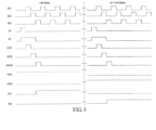
- FIG. 5 illustrates the operation timing of the shift register 100 illustrated in FIG. 1, FIG. 2 or FIG. 4 in the forward scanning mode (the first scanning direction control terminal CN is at a high level, and the second scanning direction control terminal CNB is at a low level) during two consecutive frames (i-th frame and (i+1)-th frame).
- the first pull-down node selection signal terminal PDS1 is at a high level
- the second pull-down node selection signal terminal PDS2 is at a low level.
- the first pull-down selection switching element SW10 and the second pull-down selection switching element SW11 are turned on, and the third pull-down selection switching element SW12 and the fourth pull-down selection switching element SW13 are turned off, thereby selecting the first pull-down node PD1 as the active pull-down node and causing the second pull-down node PD2 to be always at a low level.
- the fourth pull-down selection switching element SW17, the fifth pull-down selection switching element SW19 and the sixth pull-down selection switching element SW18 in the second pull-down circuit 105 whose controls terminals are connected to the second pull-down node PD2 are all turned-off, thereby causing the second pull-down circuit 105 to not operate during the i-th frame.
- the shift register 100 When the shift register 100 receives an input signal via the input terminal IN, the first input switching element SW1 and the first pull-down node reset switching element SW2 in the input circuit 101_1 are turned on, so that the potential at the pull-up node PU becomes a high level, the potential at the first pull-down node PD1 becomes a low level.
- the first output capacitor C1 and the second output capacitor C2 of the first output circuit 102 and the second output circuit 103 start to be charged, and the second output switching element SW4 and the fourth output switching element SW6 are turned on.
- the potentials at the first clock signal terminal CK1 and the second clock signal terminal CK2 are both low levels, so that no gate driving signal is outputted at the first output terminal OUT1 and the second output terminal OUT2.
- the potential at the input terminal IN becomes a low level.
- the potential at the pull-up node PU continues to be maintained at a high level via the first output capacitor C1 and the second output capacitor C2, such that the second output switching element SW4 in the first output circuit 102 and the fourth output switching element SW6 in the second output circuit 103 are still in a turned-on state.
- the potential at the first clock signal terminal CK1 becomes a high level, so that the potential at the first output terminal OUT1 becomes a high level, and thereby a gate driving signal is outputted at the first output terminal OUT1, but the second clock signal terminal CK2 remains at a low level, so there is still no gate driving signal outputted at the second output terminal OUT2.
- the potential at the reset terminal RESET of the shift register 100 becomes a high level, so that the second input switching element SW8 in the reset circuit 101_2 is turned on, thereby causing the potential at the pull-up node PU to be a low level.
- the potential at the pull-down selection control signal terminal CK3 becomes a high level, the selection control switching element SW9 in the pull-down node selection circuit 106 is turned on, so that the first pull-down node PD1 becomes a high level, and the first capacitor C3 in the pull-down node selection circuit 106 starts to be charged.
- the first pull-down switching element SW14, the second pull-down switching element SW15 and the third pull-down switching element SW16 in the first pull-down circuit 104 are turned on, so that the potentials at the pull-up node PU, the first output terminal OUT1 and the second output terminal OUT2 become a low level.
- the potential at the pull-down selection control signal terminal CK3 becomes a low level
- the potential at the first pull-down node PD1 continues to remain at a high level via the first capacitor C3 in the pull-down node selection circuit 106
- the potential at the pull-down selection control signal terminal CK3 becomes a high level again
- the potential at the first pull-up node PD1 is a high level
- the first capacitor C3 in the pull-down node selection circuit 106 starts to be charged again. This is repeated such that the potential at the first pull-down node PD1 is always a high level.
- the first pull-down node selection signal terminal PDS1 is at a low level
- the second pull-down node selection signal terminal PDS2 is at a high level.
- the first pull-down selection switching element SW10 and the second pull-down selection switching element SW11 are turned off
- the third pull-down selection switching element SW12 and the fourth pull-down selection switching element SW13 are turned on, thereby selecting the second pull-down node PD2 as the active pull-down node and causing the first pull-down node PD1 to be always at a low level.
- the first pull-down switching element SW14, the second pull-down switching element SW15 and the third pull-down switching element SW16 in the first pull-down circuit 104 whose control terminals are connected to the first pull-down node PD1 are all turned off, so that the first pull-down circuit 104 does not operate during the (i+1)-th frame.
- the operation timing of the shift register is similar to the operation timing during the i-th frame, the same contents will not be repeated. The difference is that when the potential at the pull-down selection control signal terminal CK3 becomes a high level, the selection control switching element SW9 in the pull-down node selection circuit 106 is turned on, the second pull-down node PD2 becomes a high level, and the second capacitor C4 in the pull-down node selection circuit 106 starts to be charged.
- the fourth pull-down switching element SW17, the sixth pull-down switching element SW18 and the fifth pull-down switching element SW19 in the second pull-down circuit 105 are turned on, so that the potentials at the pull-up node PU, the second output terminal OUT2 and the first output terminal OUT1 become a low level.
- the first scanning direction control terminal CN of the shift register is at a low level, and the second scanning direction control terminal CNB is at a high level.
- the reset circuit 101_2 corresponds to the input circuit 101_1 in the case of forward scanning
- the input circuit 101_1 corresponds to the reset circuit 101_2 in the case of forward scanning.
- the operation timing of the shift register in the reverse scanning mode is similar to the operation timing in the forward scanning mode, related description is omitted here.
- FIG. 5 only illustrates the case where two pull-down nodes are alternately used with one frame as a unit.
- two pull-down nodes may be alternately used with multiple frames as a unit according to needs (e.g., two pull-down nodes may be alternately used between every two frames that are adjacent, or two pull-down nodes are alternately used between one frame and three frames that are adjacent, etc.), or more pull-down nodes are arranged, and these pull-down nodes are sequentially used with one or more frames set in advance as a unit.
- the operation timing of these variant of shift registers is similar to that illustrated in FIG. 5 , the difference lies in the switching period of the pull-down node and/or the number of the pull-down nodes, related description is omitted herein.
- the duty ratio of each clock signal may be 1/3.
- the duty cycle of each clock signal may be set as smaller as needed, for example 1/4.
- the duty ratio of each clock signal may be set to 1/4.
- the duty ratio of each clock signal can be set to 1/5, and so on, and so forth.
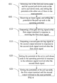
- FIG. 6 illustrates a method for driving a shift register according to the present disclosure.
- the exemplary method begins from step 601.
- the shift register selects one of the first pull-down node and the second pull-down node as the active pull-down node and sets the potential at the other one of them to the reset potential.
- a corresponding signal may be provided to the first pull-down node selection signal terminal POS1 and the second pull-down node selection signal terminal PDS2 of the shift register 100.
- the pull-down node selection circuit 106 sets one of the first pull-down node PD1 and the second pull-down node PD2 as the active pull-down node according to the potentials at the first pull-down node selection signal terminal POS1 and the second pull-down node selection signal terminal PDS2, and sets the potential at the other one of them to remain at a low level at all times.
- the first pull-down node PD1 and the second pull-down node PD2 may be alternately used as the active pull-down node in accordance with a preset number of frames.
- the shift register receives an input signal and sets the potential at the pull-up node to the operating potential.
- the shift register 100 can set the potential at the pull up node PU (including nodes PU0, PU1 and PU2) to a high level upon receiving an input signal via the input terminal IN.
- the first output terminal OUT1 and the second output terminal OUT2 both have no gate driving signal outputted.
- step 610 the shift register outputs a first gate driving signal at the first output terminal in response to receiving the first clock signal.
- the shift register 100 may output a gate driving signal at the first output terminal OUT1 when receiving the first clock signal via the first clock signal terminal CK1 terminal.
- the potential at the pull-up node PU (including the nodes PU0, PU1 and PU2) can be maintained at a high level via the capacitors in the first output circuit 102 and the second output circuit 103, and no gate driving signal is outputted at the second output terminal OUT2.
- step 615 the shift register outputs a second gate driving signal at the second output terminal in response to the second clock signal received after the first clock signal.
- the shift register 100 may output a gate driving signal at the second output terminal OUT2 when receiving the second clock signal via the second clock signal terminal CK2.
- the potential at the pull-up node PU (including the nodes PU0, PU1 and PU2) is still maintained at a high level via the capacitors in the first output circuit 102 and the second output circuit 103, and no gate driving signal is outputted at the first output terminal OUT1.
- step 620 the shift register sets the potential at the active pull-down node to the operating potential in response to the reference signal received after the second clock signal.
- the shift register 100 can cause the potential at the pull-up node PU (including the nodes PU0, PU1 and PU2) to become a low level when receiving the reference signal via the reset terminal RESET.
- the pull-down node selection circuit 106 in the shift register 100 can, in response to a third clock signal received by the shift register 100 via the pull-down selection control signal terminal CK3, set the potential at the first pull-down node PD1 or the second pull-down node PD2 selected as the active pull-down node to a high level.
- the capacitor in the pull-down node selection circuit 106 is charged while the potential at the active pull-down node is set to a high level; when the potential at the pull-down selection control signal terminal CK3 of the shift register 100 is a low level, the potential at the active pull-down node continues to remain at a high level via the capacitor in the pull-down node selection circuit 106, so that the pull-down circuit (the first pull-down circuit 104 or the second pull-down circuit 105) corresponding to the active pull-down node is still in an operating state, so that the potentials at the pull-up node PU (including the nodes PU0, PU1 and PU2), the first output terminal OUT1 and the second output terminal OUT2 remain at a low level.
- FIG. 7 illustrates an exemplary connection manner of a gate driving circuit including a shift register according to an embodiment of the present disclosure.
- Terminals of the shift register such as the reference signal terminal RS, the operating potential terminal VGH, the first scanning direction control terminal CN, the second scanning direction control terminal CNB, the first pull-down node selection signal terminal PDS1 and the second pull-down node selection signal terminal PDS2, are mainly used to receive external control signals, so these terminals of the shift register are not illustrated in FIG. 7 illustrating the cascading manner of the shift register.
- each shift register is the exemplary shift register 100 illustrated in FIG. 1, FIG. 2 or FIG. 4 .
- the shift register according to an embodiment of the present disclosure may have other variants, for example, they may have more output terminals and more clock signal terminals, and these clock signals may be set according to the relationship between the respective clock signals described above.
- the input terminal IN of the shift register SR1 at the first stage receives the frame start signal STV.
- the input terminal IN of the shift register (e.g., SR2, SR3, SR4, SR5 in FIG. 7 ) other than the first stage is connected to the second output terminal OUT2 of the corresponding shift register at a previous stage (e.g., SR1, SR2, SR3, SR4 in FIG. 7 ), that is, the shift register at the stage other than the first stage receives the gate driving signal from the second output terminal OUT2 of the corresponding shift register at the previous stage as its input signal.
- a previous stage e.g., SR1, SR2, SR3, SR4 in FIG. 7
- the reset terminal RESET of the shift register (e.g., SR1, SR2, SR3 and SR4 in FIG. 7 ) other than the last stage is connected to the first output terminal OUT1 of the corresponding shift register at the next stage (e.g., SR2, SR3, SR4 and SR5 in FIG. 7 ), that is, the shift register at the stage other than the last stage receives the gate driving signal from the first output terminal OUT1 of the corresponding shift register at a next stage as its reference signal.
- the reset terminal RESET of the last stage of shift register can, for example, receive the frame start signal STV (not illustrated in FIG. 7 ) during the reverse scanning.
- clock signals may be supplied to the shift registers at respective stages of the gate driving circuit via the timing control circuit.
- clock signals can be provided to the first clock signal terminal CK1, the second clock signal terminal CK2 and the pull-down node selection signal terminal CK3 of the shift register at respective stages via four clock signal lines(CLOCK1, CLOCK2, CLOCK3 and CLOCK4) connected to the timing control circuit 701.
- the duty ratio of each clock signal may be set to 1/4, and a falling edge of the high level of the clock signal supplied via CLOCK1 is aligned with a rising edge of the high level of the clock signal supplied via CLOCK2; a falling edge of the high level of the clock signal supplied via CLOCK2 is aligned with a rising edge of the high level of the clock signal supplied via CLOCK3; a falling edge of the high level of the clock signal supplied via CLOCK3 is aligned with a rising edge of the high level of the clock signal supplied via CLOCK4; and a falling edge of the high level of the clock signal supplied via CLOCK4 is aligned with a rising edge of the high level of the clock signal supplied via CLOCK1.
- the first clock signal terminal CK1, the second clock signal terminal CK2 and the pull-down node selection signal terminal CK3 in the shift register cascaded at an odd-numbered stage may be connected to the clock signal lines CLOCK1, CLOCK2 and CLOCK3 respectively; the first clock signal terminal CK1, the second clock signal terminal CK2 and the pull-down node selection signal terminal CK3 of the shift register cascaded at an even-numbered stage may be connected to the clock signal lines CLOCK3, CLOCK4 and CLOCK1 respectively.
- Progressive scan outputting of the unilateral gate driving circuit can be realized by providing clock signals to the shift registers at respective stages of the gate driving circuit in the configuration manner illustrated in FIG. 7 .
- FIG. 8 schematically illustrates an operation timing diagram of the gate driving circuit illustrated in FIG. 7 during two adjacent frames (i-th frame and (i+1)-th frame).
- CLOCK1 to CLOCK4 are clock signals having a duty ratio of 1/4, and as described above, a falling edge of the high level of the clock signal supplied by CLOCK1 is aligned with a rising edge of the high level of the clock signal supplied by CLOCK2; a falling edge of the high level of the clock signal provided by CLOCK2 is aligned with a rising edge of the high level of the clock signal provided by CLOCK3; a falling edge of the high level of the clock signal provided by CLOCK3 is aligned with a rising edge of the high level of the clock signal supplied by CLOCK4; and a falling edge of the high level of the clock signal provided by CLOCK4 is aligned with a rising edge of the high level of the clock signal provided by CLOCK1.
- PSD1 is at a high level, so that the first pull-down node PD1 is selected as the active pull-down node, and the potential at the second pull-down node PD2 is set to the reset potential, and the potential at the node PD1 may be set as the operating potential when the pull-down node selection signal terminal CK3 is at a high level; within the (i+1)-th frame, PSD2 is at a high level, so that the second pull-down node PD2 is selected as the active pull-down node, and the potential at the first pull-down node PD1 is set to the reset potential, and the potential at the PD2 node may be set to the operating potential when the pull-down node selection signal terminal CK3 is at a high level.
- the gate driving circuit can realize 8-channel progressive scan outputting of SR1 OUT1-SR4 OUT2 as illustrated in FIG. 8 .
- FIG. 9 illustrates another exemplary connection manner of a gate driving circuit comprising a shift register according to an embodiment of the present disclosure.
- FIG. 9 illustrates a configuration manner of clock signals for the progressive scan outputting of the bilateral gate driving circuit, with each stage of shift register having two output terminals OUT1 and OUT2 as an example.
- the bilateral gate driving circuit includes a first gate driving circuit and a second gate driving circuit each gate driving circuit including multiple shift registers.
- FIG. 9 only schematically illustrates that each gate driving circuit includes four shift registers (SR1-1, SR1-2, SR1-3, SR1-4; and SR2-1, SR2-2, SR2-3, SR2-4), and more shift registers may be included in the actual application.
- the input terminal IN of SR1-1 is connected to the frame start signal STV
- the second output terminal OUT2 of SR1-1 is connected to the input terminal IN of SR2-1
- the reset terminal RESET of SR1-1 is connected to the first output terminal OUT1 of SR2-1
- the input terminal of SR1-2 is connected to the second output terminal OUT of SR2-1
- the reset terminal RESET of SR2-1 is connected to the first output terminal OUT1 of SR1-2, and so on.
- the first clock signal terminal CK1, the second clock signal terminal CK2 and the pull-down selection signal terminal CK3 of the shift register at a respective stage of the first gate driving circuit are connected to the clock signal lines CLOCK1, CLOCK2 and CLOCK3 provided by the timing control circuit 901 respectively, and the first clock signal terminal CK1, the second clock signal terminal CK2 and the pull-down selection signal terminal CK3 of the shift register at a respective stage of the second gate driving circuit are connected to the clock signal lines CLOCK7, CLOCK8 and CLOCK5 provided by the timing control circuit 902 respectively.
- the two timing control circuits 901 and 902 illustrated in FIG. 9 may output four channels of clock signals (CLOCK1-CLOCK8) to control their respective gate driving circuits, or the same timing control circuit may also be used to output four channels of clock signals to control the gate driving circuit.
- the clock signal line CLOCK7 illustrated in FIG. 9 corresponds to CLOCK3
- the clock signal line CLOCK8 corresponds to CLOCK4
- the clock signal line CLOCK5 corresponds to CLOCK1.
- the gate driving circuit can realize bilateral scan outputting.
- the operating process of the shift register at each stage in the gate driving circuit illustrated in FIG. 7 or FIG. 9 is similar to the operating process of the exemplary shift register 100 illustrated in FIG. 5 , except that the duty ratio of each clock signal in FIG. 5 is 1/3, and the duty ratio of the clock signal received by the shift register at each stage in FIG. 7 or FIG. 9 is 1/4.
- 2*n clock signals can be supplied to the gate driving circuit by the timing control circuit, wherein the duty ratio of each clock signal can be set equal to or less than 1/(2n), and these clock signals are respectively supplied to n+1 clock signal terminals of the shift register at each stage in a manner similar to FIG. 7 or FIG. 9 .
- FIG. 10 illustrates a display device according to an embodiment of the present disclosure, wherein the display device includes two gate driving circuits: a first gate driving circuit 1001 and a second gate driving circuit 1002.
- the cascading structure inside the gate driving circuit is not illustrated in FIG. 10 , but only several shift registers SR1-SR3 are exemplarily illustrated.
- the manner in which the shift registers at respective stages of the two gate driving circuits in the display device illustrated in FIG. 10 are connected may be the manner illustrated in FIG. 9 .
- a pixel P is arranged, and a timing controller 1004 supplies clock signals to the data signal supplying circuit 1003 and the two gate driving circuits 1001, 1002.
- the scanning signal lines are sequentially numbered from top to bottom (e.g., scanning line 1, scanning line 2, scanning line 3 and the like in FIG. 10 )
- the first gate driving circuit 1001 the first output terminal OUT1 and the second output terminal OUT2 of the shift register cascaded at the i-stage (i is a positive integer) are connected to the (4i-3)-th and (4i-2)-th scanning signal lines respectively
- the second gate driving circuit 1002 the first output terminal OUT1 and the second output terminal OUT2 of the shift register cascaded at the j-th stage (j is a positive integer) are connected to the (4j-1)th and 4j-th scanning signal lines respectively.
- j is a positive integer
- the first output terminal OUT1 and the second output terminal OUT2 of the shift register SR1 at the first stage in the first gate driving circuit 1001 are connected to the scanning signal line 1 and the scanning signal line 2 respectively, and the first output terminal OUT1 and the second output terminal OUT2 of the shift register SR1 at the first stage in the second gate driving circuit 1002 are connected to the scanning signal line 3 and the scanning signal line 4 respectively, and so on.
- each shift register in the first gate driving circuit 1001 and the second gate driving circuit 1002 includes three output terminals
- the three output terminals of the shift register at the first stage in the driving circuit 1001 may be connected to the first to third scanning signal lines respectively in accordance with a manner similar to that illustrated in FIG. 10
- the three output terminals of the shift register at the first stage in the second gate driving circuit 1002 are connected to the 4th to 6th scanning signal lines respectively
- the three output terminals of the second stage shift register in the first gate driving circuit 1001 are connected to the 7th to 9th scanning signal lines respectively
- the three output terminals of the shift register at the second stage in the gate driving circuit 1002 are connected to the 10th to 12th scanning signal lines, and so on.
- a counter (not illustrated in FIG. 10 ) may be disposed. Whenever a frame start signal is sent to the first gate driving circuit 901, the value of the counter is incremented by one.
- the signals supplied to the first pull-down node selection signal terminal PDS1 and the second pull-down node selection signal terminal PDS2 of the shift register at each stage of the gate driving circuit 1001 and the second gate driving circuit 1002 may be changed by a control circuit or a processor (not illustrated in FIG. 10 ) in the display device, so that all shift registers in the first gate driving circuit 1001 and the second gate driving circuit 1002 change the corresponding active pull-down node.
- the shift register according to an embodiment of the present disclosure can support multiple outputs, and can achieve more reliable circuit reliability by setting two or more pull-down nodes in the shift register and alternately using these pull-down nodes with a predetermined number of frames as a unit.
- the shift register according to an embodiment of the present disclosure can enhance driving control capability of the single-stage shift register with relatively few switching elements.
- the gate driving circuit and the display device employing the shift register according to an embodiment of the present disclosure are more reliable, and more advantageous for implementing a narrow bezel onboard display product.
Landscapes
- Engineering & Computer Science (AREA)
- Physics & Mathematics (AREA)
- Computer Hardware Design (AREA)
- General Physics & Mathematics (AREA)
- Theoretical Computer Science (AREA)
- Chemical & Material Sciences (AREA)
- Crystallography & Structural Chemistry (AREA)
- Control Of Indicators Other Than Cathode Ray Tubes (AREA)
- Liquid Crystal Display Device Control (AREA)
Claims (11)
- Schieberegister, aufweisend:eine Eingangs- und Rücksetzschaltung (101), die mit einem Eingangsanschluss (IN), einem Pull-up-Schaltungspunkt (PU) und einem Rücksetzanschluss (RESET) verbunden ist und konfiguriert ist, ein Potential an dem Pull-up-Schaltungspunkt (PU) auf ein Betriebspotential zu setzen, wenn ein Potential an dem Eingangsanschluss (IN) das Betriebspotential ist, und das Potential an dem Pull-up-Schaltungspunkt (PU) auf ein Rücksetzpotential zu setzen, wenn ein Potential an dem Rücksetzanschluss (RESET) das Betriebspotential ist;eine erste Ausgangsschaltung (102), die mit dem Pull-up-Knoten (PU), einem ersten Steuersignalanschluss und einem ersten Ausgangsanschluss (OUT1) verbunden ist und konfiguriert ist, an dem ersten Ausgangsanschluss (OUT1) ein erstes Gate-Ansteuersignal auszugeben, wenn das Potential an dem Pull-up-Knoten (PU) und ein Potential an dem ersten Steuersignalanschluss das Betriebspotential sind; undeine zweite Ausgangsschaltung (103), die mit dem Pull-up-Schaltungspunkt (PU), einem zweiten Steuersignalanschluss und einem zweiten Ausgangsanschluss (OUT2) verbunden ist und konfiguriert ist, an dem zweiten Ausgangsanschluss (OUT2) ein zweites Gate-Ansteuersignal auszugeben, wenn das Potential an dem Pull-up-Schaltungspunkt (PU) und ein Potential an dem zweiten Steuersignalanschluss das Betriebspotential sind; undeine erste Pull-down-Schaltung (104), die mit einem ersten Pull-down-Schaltungspunkt (PD1), dem Pull-up-Schaltungspunkt (PU), dem ersten Ausgangsanschluss (OUT1) und dem zweiten Ausgangsanschluss (OUT2) verbunden und konfiguriert ist, die Potentiale an dem Pull-up-Schaltungspunkt (PU), dem ersten Ausgangsanschluss (OUT1) und dem zweiten Ausgangsanschluss (OUT2) auf das Rücksetzpotential zu setzen, wenn ein Potential an dem ersten Pull-down-Schaltungspunkt (PD1) das Betriebspotential ist; undeine zweite Pull-down-Schaltung (105), die mit einem zweiten Pull-down-Schaltungspunkt (PD2), dem Pull-up-Schaltungspunkt (PU), dem ersten Ausgangsanschluss (OUT1) und dem zweiten Ausgangsanschluss (OUT2) verbunden und konfiguriert ist, die Potentiale an dem Pull-up-Schaltungspunkt (PU), dem ersten Ausgangsanschluss (OUT1) und dem zweiten Ausgangsanschluss (OUT2) auf das Rücksetzpotential zu setzen, wenn ein Potential an dem zweiten Pull-down-Schaltungspunkt (PD2) das Betriebspotential ist,eine Pull-down-Schaltungspunkt-Auswahlschaltung (106), die mit einem ersten Pull-down-Schaltungspunkt-Auswahlsignalanschluss (PDS1), einem zweiten Pull-down-Schaltungspunkt-Auswahlsignalanschluss (PDS2), dem ersten Pull-down-Schaltungspunkt (PD1) und dem zweiten Pull-down-Schaltungspunkt (PD2) verbunden ist, und konfiguriert ist, abwechselnd einen des ersten Pull-down-Schaltungspunkts (PD1) und des zweiten Pull-down-Schaltungspunkts (PD2) als einen aktiven Pull-down-Schaltungspunkt gemäß dem Potential an dem ersten Pull-down-Schaltungspunkt-Auswahlsignalanschluss (PDS1) und dem Potential an dem zweiten Pull-down-Schaltungspunkt-Auswahlsignalanschluss (PDS2) auszuwählen, wobei ein Potential an dem ausgewählten aktiven Pull-down-Schaltungspunkt das Betriebspotential ist; undwobei die Pull-down-Schaltungspunkt-Auswahlschaltung (106) aufweist:ein erstes Pull-down-Auswahlschaltelement (SW10), dessen Steueranschluss mit dem ersten Pull-down-Knoten-Auswahlsignalanschluss (PDS1) verbunden ist, und dessen erster oder zweiter Anschluss mit dem ersten Pull-down-Knoten (PD1) verbunden ist;ein zweites Pull-down-Schaltelement (SW11), dessen Steueranschluss mit dem ersten Pull-down-Schaltungspunkt-Auswahlsignalanschluss (PDS1) verbunden ist, wobei einer von dessen erstem und zweitem Anschluss mit dem zweiten Pull-down-Schaltungspunkt (PD2) verbunden ist, und der andere von dessen erstem und zweitem Anschluss mit einem Referenzsignalanschluss (RS) verbunden ist;ein drittes Pull-down-Auswahlschaltelement (SW12), dessen Steueranschluss mit dem zweiten Pull-down-Schaltungspunkt-Auswahlsignalanschluss (PDS2) verbunden ist, wobei einer von dessen erstem Anschluss und zweitem Anschluss mit dem zweiten Pull-down-Schaltungspunkt (PD2) verbunden ist, und der andere von dessen erstem Anschluss und zweitem Anschluss mit dem anderen von dessen erstem Anschluss und zweitem Anschluss des ersten Pull-down-Auswahlschaltelements verbunden ist; undein viertes Pull-down-Auswahlschaltelement (SW13), dessen Steueranschluss mit dem zweiten Pull-down-Schaltungspunkt-Auswahlsignalanschluss (PDS2) verbunden ist, wobei einer von dessen erstem Anschluss und zweitem Anschluss mit dem ersten Pull-down-Schaltungspunkt (PD1) verbunden ist und der andere von dessen erstem Anschluss und zweitem Anschluss mit dem Referenzsignalanschluss (RS) verbunden ist.
- Schieberegister nach Anspruch 1, wobei die Pull-down-Schaltungspunkt-Auswahlschaltung (106) weiter aufweist:einen ersten Kondensator (C3), der zwischen den ersten Pull-down-Schaltungspunkt (PD1) und den Referenzsignalanschluss (RS) geschaltet ist; undeinen zweiten Kondensator (C4), der zwischen den zweiten Pull-down-Schaltungspunkt (PD2) und den Referenzsignalanschluss (RS) geschaltet ist.
- Schieberegister nach Anspruch 1, wobei die Pull-down-Schaltungspunkt-Auswahlschaltung (106) weiter aufweist:
ein Auswahl-Steuerschaltelement (SW9), wobei dessen Steueranschluss und einer von dessen erstem Anschluss und zweitem Anschluss beide mit dem Pull-down-Auswahl-Steuersignalanschluss verbunden sind, und der andere von dessen erstem Anschluss und zweitem Anschluss mit dem anderen von dessen erstem Anschluss und zweitem Anschluss des ersten Pull-down-Auswahlschaltelements (SW10) und mit dem anderen von dessen erstem Anschluss und zweitem Anschluss des dritten Pull-down-Auswahlschaltelements (SW12) verbunden ist. - Schieberegister nach einem der Ansprüche 1 oder 2, wobei die Eingabe- und Rücksetzschaltung (101) aufweist:ein erstes Eingangsschaltelement (SW1), wobei dessen Steueranschluss mit dem Eingangsanschluss (IN) verbunden ist, wobei einer von dessen erstem und zweitem Anschluss mit einem ersten Abtast-Steuersignalanschluss verbunden ist, und der andere von dessen erstem und zweitem Anschluss mit dem Pull-up-Schaltungspunkt (PU) verbunden ist;und ein zweites Eingangsschaltelement (SW8), wobei dessen Steueranschluss mit dem Rücksetzanschluss (RESET) verbunden ist, einer von dessen erstem und zweitem Anschluss mit einem zweiten Abtast-Steuersignalanschluss verbunden ist, und der andere von dessen erstem und zweitem Anschluss mit dem Pull-up-Schaltungspunkt (PU) verbunden ist,wobei das Potential eines ersten Abtaststeuersignals das Betriebspotential ist und das Potential eines zweiten Abtaststeuersignals das Rücksetzpotential während einer Vorwärtsabtastung ist, und das Potential des ersten Abtaststeuersignals das Rücksetzpotential ist und das Potential des zweiten Abtaststeuersignals das Betriebspotential während einer Rückwärtsabtastung ist.
- Schieberegister nach Anspruch 4, wobei die Eingangs- und Rücksetzschaltung (101) ferner aufweist:
ein erstes Pull-down-Schaltungspunkt-Rücksetzschaltelement (SW2), dessen Steueranschluss mit dem Pull-up-Schaltungspunkt (PU) verbunden ist, wobei einer von dessen erstem und zweitem Anschluss mit dem ersten Pull-up-Schaltungspunkt (PD1) verbunden ist, und der andere von dessen erstem und zweitem Anschluss mit dem Referenzsignal-Anschluss (RS) verbunden ist; und ein zweites Pull-down-Schaltungspunkt-Rücksetzschaltelement (SW3), dessen Steueranschluss mit dem Pull-up-Schaltungspunkt (PU) verbunden ist, einer von dessen erstem und zweitem Anschluss mit dem zweiten Pull-down-Schaltungspunkt (PD2) verbunden ist und der andere von dessen erstem und zweitem Anschluss mit dem Referenzsignalanschluss (RS) verbunden ist. - Schieberegister nach einem der Ansprüche 1 oder 2, wobei die erste Ausgangsschaltung (102) aufweist:ein erstes Ausgangsschaltelement (SW5), wobei dessen Steueranschluss mit einem Betriebspotentialanschluss verbunden ist und einer von dessen erstem und zweitem Schaltungspunkt mit dem Pull-up-Schaltungspunkt (PU) verbunden ist;ein zweites Ausgangsschaltelement (SW4), wobei dessen Steueranschluss mit dem anderen von dem ersten Anschluss und dem zweiten Anschluss des ersten Ausgangsschaltelements verbunden ist, wobei einer von dessen erstem Anschluss und zweitem Anschluss mit dem ersten Steuersignalanschluss verbunden ist und der andere von dessen erstem Anschluss und zweitem Anschluss mit dem ersten Ausgangsanschluss (OUT1) verbunden ist; undeinen ersten Ausgangskondensator (C1), der zwischen den Steueranschluss des zweiten Ausgangsschaltelements und den ersten Ausgangsanschluss (OUT1) geschaltet ist.
- Schieberegister nach einem der Ansprüche 1 bis 3, wobei die zweite Ausgangsschaltung (103) aufweist:ein drittes Ausgangsschaltelement (SW7), wobei dessen Steueranschluss mit dem Betriebspotentialanschluss verbunden ist und einer von dessen erstem und zweitem Anschluss mit dem Pull-up-Schaltungspunkt (PU) verbunden ist;ein viertes Ausgangsschaltelement (SW6), dessen Steueranschluss mit dem anderen des ersten Anschlusses und des zweiten Anschlusses des dritten Ausgangsschaltelements verbunden ist, wobei einer von dessen erstem Anschluss und zweitem Anschluss mit dem zweiten Steuersignalanschluss verbunden ist und der andere von dessen erstem Anschluss und zweitem Anschluss mit dem zweiten Ausgangsanschluss (OUT2) verbunden ist; undeinen zweiten Ausgangskondensator (C2), der zwischen dem Steueranschluss des vierten Ausgangsschaltelements und dem zweiten Ausgangsanschluss (OUT2) geschaltet ist.
- Schieberegister nach einem der Ansprüche 1 bis 3, wobei die erste Pull-Down-Schaltung (104) aufweist:ein erstes Pull-down-Schaltelement (SW14), dessen Steueranschluss mit dem ersten Pull-down-Schaltungspunkt (PD1) verbunden ist, wobei einer von dessen erstem und zweitem Anschluss mit dem Pull-up-Schaltungspunkt (PU) verbunden ist, und der andere von dessen erstem und zweitem Anschluss mit dem Referenzsignal-Anschluss (RS) verbunden ist;ein zweites Pull-down-Schaltelement (SW15), dessen Schaltungspunkt mit dem ersten Pull-down-Knoten (PD1) verbunden ist, wobei einer von dessen erstem und zweitem Anschluss mit dem ersten Ausgangsanschluss (OUT1) verbunden ist, und der andere von dessen erstem und zweitem Anschluss mit dem Referenzsignalanschluss (RS) verbunden ist;ein drittes Pull-down-Schaltelement (SW16), dessen Steueranschlusspunkt mit dem ersten Pull-down-Schaltungspunkt (PD1) verbunden ist, wobei einer von dessen erstem und zweitem Anschluss mit dem zweiten Ausgangsanschluss (OUT2) verbunden ist, und der andere von dessen erstem und zweitem Anschluss mit dem Referenzsignalanschluss (RS) verbunden ist.
- Schieberegister nach einem der Ansprüche 1 bis 3, wobei die zweite Pull-Down-Schaltung (105) aufweist:ein viertes Pull-down-Schaltelement (SW17), wobei dessen Steueranschluss mit dem zweiten Pull-down-Schaltungspunkt (PD2) verbunden ist, wobei einer von dessen erstem und zweitem Anschluss mit dem Pull-up-Schaltungspunkt (PU) verbunden ist, und wobei der andere von dessen erstem und zweitem Anschluss mit dem Referenzsignal-Anschluss (RS) verbunden ist;ein fünftes Pull-down-Schaltelement (SW19), dessen Steueranschluss mit dem zweiten Pull-down-Knoten (PD2) verbunden ist, wobei einer von dessen erstem und zweitem Anschluss mit dem ersten Ausgangsanschluss (OUT1) verbunden ist, und der andere von dessen erstem und zweitem Anschluss mit dem Referenzsignalanschluss (RS) verbunden ist;und ein sechstes Pull-down-Schaltelement (SW18), dessen Steueranschluss mit dem zweiten Pull-down-Schaltungspunkt (PD2) verbunden ist, wobei einer von dessen erstem und zweitem Anschluss mit dem zweiten Ausgangsanschluss (OUT2) verbunden ist, und der andere von dessen erstem und zweitem Anschluss mit dem Referenzsignalanschluss (RS) verbunden ist.
- Gate-Treiberschaltung, die mehrere kaskadierte Schieberegister nach einem der Ansprüche 1 bis 9 aufweist, wobeimit Ausnahme des Schieberegisters in einer ersten Stufe ein Eingangsanschluss des Schieberegisters in jeder der anderen Stufen mit einem zweiten Ausgangsanschluss des kaskadierten Schieberegisters in einer vorhergehenden Stufe verbunden ist, undmit Ausnahme des Schieberegisters in einer letzten Stufe ein Rücksetzanschluss des Schieberegisters in jeder der anderen Stufen mit einem ersten Ausgangsanschluss des Schieberegisters in einer nächsten Stufe verbunden ist.
- Anzeigeeinrichtung, die eine erste Gate-Ansteuerungsschaltung und eine zweite Gate-Ansteuerungsschaltung aufweist, wobei die erste Gate-Ansteuerungsschaltung N kaskadierte Schieberegister nach einem der Ansprüche 1 bis 9 aufweist, die zweite Gate-Ansteuerungsschaltung N kaskadierte Schieberegister nach einem der Ansprüche 1 bis 9 aufweist; wobeiein Rücksetzanschluss des Schieberegisters in einer ersten Stufe der ersten Gate-Ansteuerungsschaltung mit einem ersten Ausgangsanschluss des Schieberegisters in der ersten Stufe einer zweiten Gate-Ansteuerungsschaltung verbunden ist;ein Eingangsanschluss des Schieberegisters an einer i-ten Stufe der ersten Gate-Ansteuerschaltung mit einem zweiten Ausgangsanschluss des Schieberegisters an einer (i-1)-ten Stufe der zweiten Gate-Ansteuerschaltung verbunden ist, und ein Rücksetzanschluss des Schieberegisters an der i-ten Stufe der ersten Gate-Ansteuerschaltung mit einem ersten Ausgangsanschluss des Schieberegisters an der i-ten Stufe der zweiten Gate-Ansteuerschaltung verbunden ist, wobei 1<i≤N;ein Eingangsanschluss des Schieberegisters in einer j-ten Stufe der zweiten Gate-Ansteuerschaltung mit einem zweiten Ausgangsanschluss des Schieberegisters in einer j-ten Stufe der ersten Gate-Ansteuerschaltung verbunden ist, und ein Rücksetzanschluss des Schieberegisters in der j-ten Stufe der zweiten Gate-Ansteuerschaltung mit einem ersten Ausgangsanschluss des Schieberegisters in einer (j+1)-ten Stufe der ersten Gate-Ansteuerschaltung verbunden ist, wobei 1≤j<N.
Applications Claiming Priority (2)
| Application Number | Priority Date | Filing Date | Title |
|---|---|---|---|
| CN201711204895.0A CN109841194B (zh) | 2017-11-27 | 2017-11-27 | 移位寄存器及其驱动方法、栅极驱动电路和显示装置 |
| PCT/CN2018/105694 WO2019100822A1 (zh) | 2017-11-27 | 2018-09-14 | 移位寄存器及其驱动方法、栅极驱动电路和显示装置 |
Publications (3)
| Publication Number | Publication Date |
|---|---|
| EP3719783A1 EP3719783A1 (de) | 2020-10-07 |
| EP3719783A4 EP3719783A4 (de) | 2021-08-18 |
| EP3719783B1 true EP3719783B1 (de) | 2025-03-26 |
Family
ID=66631794
Family Applications (1)
| Application Number | Title | Priority Date | Filing Date |
|---|---|---|---|
| EP18855161.8A Active EP3719783B1 (de) | 2017-11-27 | 2018-09-14 | Schieberegister, ansteuerungsverfahren dafür, gatetreiberschaltung und anzeigevorrichtung |
Country Status (4)
| Country | Link |
|---|---|
| US (1) | US10950319B2 (de) |
| EP (1) | EP3719783B1 (de) |
| CN (1) | CN109841194B (de) |
| WO (1) | WO2019100822A1 (de) |
Families Citing this family (12)
| Publication number | Priority date | Publication date | Assignee | Title |
|---|---|---|---|---|
| US12347402B2 (en) * | 2019-01-09 | 2025-07-01 | HKC Corporation Limited | Display panel, driving method, and display device |
| CN110930942B (zh) * | 2019-11-28 | 2020-11-27 | 厦门天马微电子有限公司 | 移位寄存器及其控制方法、显示面板 |
| CN113763854B (zh) * | 2020-06-05 | 2024-05-17 | 深超光电(深圳)有限公司 | 移位寄存器及具有移位寄存器的显示装置 |
| US11756499B2 (en) * | 2021-01-19 | 2023-09-12 | Tcl China Star Optoelectronics Technology Co., Ltd. | Scan driving circuit with register part and pull-down part and display panel |
| CN112863586B (zh) | 2021-01-26 | 2024-10-22 | 京东方科技集团股份有限公司 | 移位寄存器及其控制方法、栅极驱动电路和显示面板 |
| JP7777133B2 (ja) * | 2021-05-27 | 2025-11-27 | 京東方科技集團股▲ふん▼有限公司 | 表示基板及びその製造方法、表示装置 |
| US12525191B2 (en) * | 2021-06-18 | 2026-01-13 | Boe Technology Group Co., Ltd. | Display substrate and display device |
| CN117063237A (zh) * | 2022-03-14 | 2023-11-14 | 京东方科技集团股份有限公司 | 移位寄存器单元及其驱动方法、栅极驱动电路及显示装置 |
| CN114842787B (zh) * | 2022-04-26 | 2025-04-25 | 深圳市华星光电半导体显示技术有限公司 | 显示面板 |
| CN117642809B (zh) | 2022-06-29 | 2026-03-17 | 京东方科技集团股份有限公司 | 显示驱动电路和显示装置 |
| CN115497996B (zh) * | 2022-09-06 | 2026-01-02 | 武汉天马微电子有限公司 | 显示面板及显示装置 |
| CN117746766A (zh) * | 2023-12-29 | 2024-03-22 | 厦门天马光电子有限公司 | 栅极驱动单元及其驱动方法、移位寄存电路和显示装置 |
Family Cites Families (12)
| Publication number | Priority date | Publication date | Assignee | Title |
|---|---|---|---|---|
| JP2005235311A (ja) * | 2004-02-19 | 2005-09-02 | Olympus Corp | 信号伝送回路 |
| CN103021318B (zh) * | 2012-12-14 | 2016-02-17 | 京东方科技集团股份有限公司 | 移位寄存器及其工作方法、栅极驱动装置、显示装置 |
| CN103489484B (zh) * | 2013-09-22 | 2015-03-25 | 京东方科技集团股份有限公司 | 一种移位寄存器单元及栅极驱动电路 |
| CN105096865B (zh) * | 2015-08-06 | 2018-09-07 | 京东方科技集团股份有限公司 | 移位寄存器的输出控制单元、移位寄存器及其驱动方法以及栅极驱动装置 |
| CN104966506B (zh) * | 2015-08-06 | 2017-06-06 | 京东方科技集团股份有限公司 | 一种移位寄存器、显示面板的驱动方法及相关装置 |
| CN105652535B (zh) * | 2016-01-21 | 2018-09-11 | 武汉华星光电技术有限公司 | 一种栅极驱动电路及显示面板 |
| CN105513525B (zh) * | 2016-02-02 | 2018-03-27 | 京东方科技集团股份有限公司 | 移位寄存器单元、移位寄存器、栅极驱动电路及显示装置 |
| CN106157912B (zh) * | 2016-08-30 | 2018-10-30 | 合肥京东方光电科技有限公司 | 移位寄存器单元、其驱动方法、栅极驱动电路及显示装置 |
| CN106601168A (zh) * | 2016-12-22 | 2017-04-26 | 上海中航光电子有限公司 | 扫描单元、栅极驱动电路 |
| CN106601177B (zh) * | 2017-02-08 | 2019-10-25 | 上海天马有机发光显示技术有限公司 | 移位寄存器及其驱动方法、驱动电路和显示装置 |
| CN106652964B (zh) * | 2017-03-10 | 2019-11-05 | 京东方科技集团股份有限公司 | 移位寄存器单元及其驱动方法、栅极驱动电路、显示装置 |
| CN106910451B (zh) * | 2017-04-28 | 2020-09-29 | 昆山龙腾光电股份有限公司 | 栅极驱动电路和栅极驱动电路的驱动方法 |
-
2017
- 2017-11-27 CN CN201711204895.0A patent/CN109841194B/zh active Active
-
2018
- 2018-09-14 EP EP18855161.8A patent/EP3719783B1/de active Active
- 2018-09-14 US US16/339,752 patent/US10950319B2/en active Active
- 2018-09-14 WO PCT/CN2018/105694 patent/WO2019100822A1/zh not_active Ceased
Also Published As
| Publication number | Publication date |
|---|---|
| CN109841194B (zh) | 2020-04-10 |
| EP3719783A1 (de) | 2020-10-07 |
| CN109841194A (zh) | 2019-06-04 |
| EP3719783A4 (de) | 2021-08-18 |
| WO2019100822A1 (zh) | 2019-05-31 |
| US10950319B2 (en) | 2021-03-16 |
| US20200286570A1 (en) | 2020-09-10 |
Similar Documents
| Publication | Publication Date | Title |
|---|---|---|
| EP3719783B1 (de) | Schieberegister, ansteuerungsverfahren dafür, gatetreiberschaltung und anzeigevorrichtung | |
| EP3832635B1 (de) | Schieberegister, gate-treiberschaltung, anzeigevorrichtung und gate-treiberverfahren | |
| EP3306602B1 (de) | Schieberegister, ansteuerungsschaltung für gate-elektrode und anzeigevorrichtung | |
| EP2562761B1 (de) | Schieberegister, gate-betriebsvorrichtung und datenlinien-betriebsvorrichtung für flüssigkristallanzeige | |
| TWI445309B (zh) | 閘極位移暫存器及具有該暫存器之顯示裝置 | |
| US9626895B2 (en) | Gate driving circuit | |
| US10490133B2 (en) | Shift register module and display driving circuit thereof | |
| JP6227530B2 (ja) | ゲートドライバ集積回路、シフトレジスタ及びディスプレイスクリーン | |
| US10217391B2 (en) | Shift register unit, gate driving circuit and driving method thereof, and display apparatus | |
| US10283038B2 (en) | Shift register unit and method for driving the same, gate drive circuit and display device | |
| US9508449B2 (en) | Liquid crystal display and bidirectional shift register device thereof | |
| US8253680B2 (en) | Shift register | |
| KR101863332B1 (ko) | 주사 구동부, 이를 포함하는 표시 장치 및 그 구동 방법 | |
| CN103915052B (zh) | 一种栅极驱动电路、方法及显示装置 | |
| KR101552408B1 (ko) | 주사 신호선 구동 회로 및 주사 신호선 구동 방법 | |
| US9286846B2 (en) | Liquid crystal display and bidirectional shift register apparatus thereof | |
| US7466312B2 (en) | Level shifter circuit and method for controlling voltage levels of clock signal and inverted clock signal for driving gate lines of amorphous silicon gate-thin film transistor liquid crystal display | |
| US20180335814A1 (en) | Shift register unit, gate drive circuit and display apparatus having the same, and driving method thereof | |
| US20140064437A1 (en) | Shift register and driving method thereof, gate driving apparatus and display apparatus | |
| US20150332784A1 (en) | Shift register unit, shift register, gate drive circuit and display apparatus | |
| KR20100108301A (ko) | 액정 디스플레이 게이트 구동 장치 | |
| US20170025079A1 (en) | Shift register unit and driving method thereof, gate driving circuit and display device | |
| CN104966503B (zh) | 一种栅极驱动电路及其驱动方法、电平移位器 | |
| KR102460921B1 (ko) | 시프트레지스터 및 이를 포함하는 표시장치 | |
| KR20140147203A (ko) | 쉬프트 레지스터 및 이를 포함하는 평판 표시 장치 |
Legal Events
| Date | Code | Title | Description |
|---|---|---|---|
| STAA | Information on the status of an ep patent application or granted ep patent |
Free format text: STATUS: UNKNOWN |
|
| STAA | Information on the status of an ep patent application or granted ep patent |
Free format text: STATUS: THE INTERNATIONAL PUBLICATION HAS BEEN MADE |
|
| PUAI | Public reference made under article 153(3) epc to a published international application that has entered the european phase |
Free format text: ORIGINAL CODE: 0009012 |
|
| STAA | Information on the status of an ep patent application or granted ep patent |
Free format text: STATUS: REQUEST FOR EXAMINATION WAS MADE |
|
| 17P | Request for examination filed |
Effective date: 20190321 |
|
| AK | Designated contracting states |
Kind code of ref document: A1 Designated state(s): AL AT BE BG CH CY CZ DE DK EE ES FI FR GB GR HR HU IE IS IT LI LT LU LV MC MK MT NL NO PL PT RO RS SE SI SK SM TR |
|
| AX | Request for extension of the european patent |
Extension state: BA ME |
|
| DAV | Request for validation of the european patent (deleted) | ||
| DAX | Request for extension of the european patent (deleted) | ||
| REG | Reference to a national code |
Ref country code: DE Ref legal event code: R079 Free format text: PREVIOUS MAIN CLASS: G09G0003200000 Ipc: G09G0003360000 Ref country code: DE Ref legal event code: R079 Ref document number: 602018080551 Country of ref document: DE Free format text: PREVIOUS MAIN CLASS: G09G0003200000 Ipc: G09G0003360000 |
|
| A4 | Supplementary search report drawn up and despatched |
Effective date: 20210720 |
|
| RIC1 | Information provided on ipc code assigned before grant |
Ipc: G09G 3/36 20060101AFI20210714BHEP |
|
| STAA | Information on the status of an ep patent application or granted ep patent |
Free format text: STATUS: EXAMINATION IS IN PROGRESS |
|
| 17Q | First examination report despatched |
Effective date: 20230620 |
|
| GRAP | Despatch of communication of intention to grant a patent |
Free format text: ORIGINAL CODE: EPIDOSNIGR1 |
|
| STAA | Information on the status of an ep patent application or granted ep patent |
Free format text: STATUS: GRANT OF PATENT IS INTENDED |
|
| INTG | Intention to grant announced |
Effective date: 20241209 |
|
| GRAS | Grant fee paid |
Free format text: ORIGINAL CODE: EPIDOSNIGR3 |
|
| GRAA | (expected) grant |
Free format text: ORIGINAL CODE: 0009210 |
|
| STAA | Information on the status of an ep patent application or granted ep patent |
Free format text: STATUS: THE PATENT HAS BEEN GRANTED |
|
| AK | Designated contracting states |
Kind code of ref document: B1 Designated state(s): AL AT BE BG CH CY CZ DE DK EE ES FI FR GB GR HR HU IE IS IT LI LT LU LV MC MK MT NL NO PL PT RO RS SE SI SK SM TR |
|
| REG | Reference to a national code |
Ref country code: GB Ref legal event code: FG4D |
|
| REG | Reference to a national code |
Ref country code: CH Ref legal event code: EP |
|
| REG | Reference to a national code |
Ref country code: DE Ref legal event code: R096 Ref document number: 602018080551 Country of ref document: DE |
|
| REG | Reference to a national code |
Ref country code: IE Ref legal event code: FG4D |
|
| PG25 | Lapsed in a contracting state [announced via postgrant information from national office to epo] |
Ref country code: RS Free format text: LAPSE BECAUSE OF FAILURE TO SUBMIT A TRANSLATION OF THE DESCRIPTION OR TO PAY THE FEE WITHIN THE PRESCRIBED TIME-LIMIT Effective date: 20250626 |
|
| PG25 | Lapsed in a contracting state [announced via postgrant information from national office to epo] |
Ref country code: FI Free format text: LAPSE BECAUSE OF FAILURE TO SUBMIT A TRANSLATION OF THE DESCRIPTION OR TO PAY THE FEE WITHIN THE PRESCRIBED TIME-LIMIT Effective date: 20250326 |
|
| REG | Reference to a national code |
Ref country code: LT Ref legal event code: MG9D |
|
| PG25 | Lapsed in a contracting state [announced via postgrant information from national office to epo] |
Ref country code: NO Free format text: LAPSE BECAUSE OF FAILURE TO SUBMIT A TRANSLATION OF THE DESCRIPTION OR TO PAY THE FEE WITHIN THE PRESCRIBED TIME-LIMIT Effective date: 20250626 |
|
| PG25 | Lapsed in a contracting state [announced via postgrant information from national office to epo] |
Ref country code: HR Free format text: LAPSE BECAUSE OF FAILURE TO SUBMIT A TRANSLATION OF THE DESCRIPTION OR TO PAY THE FEE WITHIN THE PRESCRIBED TIME-LIMIT Effective date: 20250326 |
|
| PG25 | Lapsed in a contracting state [announced via postgrant information from national office to epo] |
Ref country code: LV Free format text: LAPSE BECAUSE OF FAILURE TO SUBMIT A TRANSLATION OF THE DESCRIPTION OR TO PAY THE FEE WITHIN THE PRESCRIBED TIME-LIMIT Effective date: 20250326 |
|
| PG25 | Lapsed in a contracting state [announced via postgrant information from national office to epo] |
Ref country code: GR Free format text: LAPSE BECAUSE OF FAILURE TO SUBMIT A TRANSLATION OF THE DESCRIPTION OR TO PAY THE FEE WITHIN THE PRESCRIBED TIME-LIMIT Effective date: 20250627 Ref country code: BG Free format text: LAPSE BECAUSE OF FAILURE TO SUBMIT A TRANSLATION OF THE DESCRIPTION OR TO PAY THE FEE WITHIN THE PRESCRIBED TIME-LIMIT Effective date: 20250326 |
|
| REG | Reference to a national code |
Ref country code: NL Ref legal event code: MP Effective date: 20250326 |
|
| PG25 | Lapsed in a contracting state [announced via postgrant information from national office to epo] |
Ref country code: NL Free format text: LAPSE BECAUSE OF FAILURE TO SUBMIT A TRANSLATION OF THE DESCRIPTION OR TO PAY THE FEE WITHIN THE PRESCRIBED TIME-LIMIT Effective date: 20250326 |
|
| PG25 | Lapsed in a contracting state [announced via postgrant information from national office to epo] |
Ref country code: SE Free format text: LAPSE BECAUSE OF FAILURE TO SUBMIT A TRANSLATION OF THE DESCRIPTION OR TO PAY THE FEE WITHIN THE PRESCRIBED TIME-LIMIT Effective date: 20250326 |
|
| REG | Reference to a national code |
Ref country code: AT Ref legal event code: MK05 Ref document number: 1779775 Country of ref document: AT Kind code of ref document: T Effective date: 20250326 |
|
| PG25 | Lapsed in a contracting state [announced via postgrant information from national office to epo] |
Ref country code: SM Free format text: LAPSE BECAUSE OF FAILURE TO SUBMIT A TRANSLATION OF THE DESCRIPTION OR TO PAY THE FEE WITHIN THE PRESCRIBED TIME-LIMIT Effective date: 20250326 |
|
| PG25 | Lapsed in a contracting state [announced via postgrant information from national office to epo] |
Ref country code: ES Free format text: LAPSE BECAUSE OF FAILURE TO SUBMIT A TRANSLATION OF THE DESCRIPTION OR TO PAY THE FEE WITHIN THE PRESCRIBED TIME-LIMIT Effective date: 20250326 Ref country code: PT Free format text: LAPSE BECAUSE OF FAILURE TO SUBMIT A TRANSLATION OF THE DESCRIPTION OR TO PAY THE FEE WITHIN THE PRESCRIBED TIME-LIMIT Effective date: 20250728 |
|
| PGFP | Annual fee paid to national office [announced via postgrant information from national office to epo] |
Ref country code: DE Payment date: 20250919 Year of fee payment: 8 |
|
| PG25 | Lapsed in a contracting state [announced via postgrant information from national office to epo] |
Ref country code: PL Free format text: LAPSE BECAUSE OF FAILURE TO SUBMIT A TRANSLATION OF THE DESCRIPTION OR TO PAY THE FEE WITHIN THE PRESCRIBED TIME-LIMIT Effective date: 20250326 Ref country code: IT Free format text: LAPSE BECAUSE OF FAILURE TO SUBMIT A TRANSLATION OF THE DESCRIPTION OR TO PAY THE FEE WITHIN THE PRESCRIBED TIME-LIMIT Effective date: 20250326 |
|
| PG25 | Lapsed in a contracting state [announced via postgrant information from national office to epo] |
Ref country code: AT Free format text: LAPSE BECAUSE OF FAILURE TO SUBMIT A TRANSLATION OF THE DESCRIPTION OR TO PAY THE FEE WITHIN THE PRESCRIBED TIME-LIMIT Effective date: 20250326 |
|
| PG25 | Lapsed in a contracting state [announced via postgrant information from national office to epo] |
Ref country code: EE Free format text: LAPSE BECAUSE OF FAILURE TO SUBMIT A TRANSLATION OF THE DESCRIPTION OR TO PAY THE FEE WITHIN THE PRESCRIBED TIME-LIMIT Effective date: 20250326 |
|
| PG25 | Lapsed in a contracting state [announced via postgrant information from national office to epo] |
Ref country code: RO Free format text: LAPSE BECAUSE OF FAILURE TO SUBMIT A TRANSLATION OF THE DESCRIPTION OR TO PAY THE FEE WITHIN THE PRESCRIBED TIME-LIMIT Effective date: 20250326 |
|
| PG25 | Lapsed in a contracting state [announced via postgrant information from national office to epo] |
Ref country code: SK Free format text: LAPSE BECAUSE OF FAILURE TO SUBMIT A TRANSLATION OF THE DESCRIPTION OR TO PAY THE FEE WITHIN THE PRESCRIBED TIME-LIMIT Effective date: 20250326 |
|
| PG25 | Lapsed in a contracting state [announced via postgrant information from national office to epo] |
Ref country code: IS Free format text: LAPSE BECAUSE OF FAILURE TO SUBMIT A TRANSLATION OF THE DESCRIPTION OR TO PAY THE FEE WITHIN THE PRESCRIBED TIME-LIMIT Effective date: 20250726 |
|
| REG | Reference to a national code |
Ref country code: DE Ref legal event code: R097 Ref document number: 602018080551 Country of ref document: DE |
|
| PG25 | Lapsed in a contracting state [announced via postgrant information from national office to epo] |
Ref country code: DK Free format text: LAPSE BECAUSE OF FAILURE TO SUBMIT A TRANSLATION OF THE DESCRIPTION OR TO PAY THE FEE WITHIN THE PRESCRIBED TIME-LIMIT Effective date: 20250326 |
|
| PG25 | Lapsed in a contracting state [announced via postgrant information from national office to epo] |
Ref country code: CZ Free format text: LAPSE BECAUSE OF FAILURE TO SUBMIT A TRANSLATION OF THE DESCRIPTION OR TO PAY THE FEE WITHIN THE PRESCRIBED TIME-LIMIT Effective date: 20250326 |
|
| PLBE | No opposition filed within time limit |
Free format text: ORIGINAL CODE: 0009261 |
|
| STAA | Information on the status of an ep patent application or granted ep patent |
Free format text: STATUS: NO OPPOSITION FILED WITHIN TIME LIMIT |
|
| REG | Reference to a national code |
Ref country code: CH Ref legal event code: L10 Free format text: ST27 STATUS EVENT CODE: U-0-0-L10-L00 (AS PROVIDED BY THE NATIONAL OFFICE) Effective date: 20260211 |
|
| 26N | No opposition filed |
Effective date: 20260105 |