EP3719786B1 - Circuit de pixel et son procédé de pilotage, et panneau d'affichage et appareil d'affichage - Google Patents
Circuit de pixel et son procédé de pilotage, et panneau d'affichage et appareil d'affichage Download PDFInfo
- Publication number
- EP3719786B1 EP3719786B1 EP18855189.9A EP18855189A EP3719786B1 EP 3719786 B1 EP3719786 B1 EP 3719786B1 EP 18855189 A EP18855189 A EP 18855189A EP 3719786 B1 EP3719786 B1 EP 3719786B1
- Authority
- EP
- European Patent Office
- Prior art keywords
- transistor
- circuit
- terminal
- sub
- electrode
- Prior art date
- Legal status (The legal status is an assumption and is not a legal conclusion. Google has not performed a legal analysis and makes no representation as to the accuracy of the status listed.)
- Active
Links
Images




Classifications
-
- G—PHYSICS
- G09—EDUCATION; CRYPTOGRAPHY; DISPLAY; ADVERTISING; SEALS
- G09G—ARRANGEMENTS OR CIRCUITS FOR CONTROL OF INDICATING DEVICES USING STATIC MEANS TO PRESENT VARIABLE INFORMATION
- G09G3/00—Control arrangements or circuits, of interest only in connection with visual indicators other than cathode-ray tubes
- G09G3/20—Control arrangements or circuits, of interest only in connection with visual indicators other than cathode-ray tubes for presentation of an assembly of a number of characters, e.g. a page, by composing the assembly by combination of individual elements arranged in a matrix no fixed position being assigned to or needed to be assigned to the individual characters or partial characters
- G09G3/22—Control arrangements or circuits, of interest only in connection with visual indicators other than cathode-ray tubes for presentation of an assembly of a number of characters, e.g. a page, by composing the assembly by combination of individual elements arranged in a matrix no fixed position being assigned to or needed to be assigned to the individual characters or partial characters using controlled light sources
- G09G3/30—Control arrangements or circuits, of interest only in connection with visual indicators other than cathode-ray tubes for presentation of an assembly of a number of characters, e.g. a page, by composing the assembly by combination of individual elements arranged in a matrix no fixed position being assigned to or needed to be assigned to the individual characters or partial characters using controlled light sources using electroluminescent panels
- G09G3/32—Control arrangements or circuits, of interest only in connection with visual indicators other than cathode-ray tubes for presentation of an assembly of a number of characters, e.g. a page, by composing the assembly by combination of individual elements arranged in a matrix no fixed position being assigned to or needed to be assigned to the individual characters or partial characters using controlled light sources using electroluminescent panels semiconductive, e.g. using light-emitting diodes [LED]
- G09G3/3208—Control arrangements or circuits, of interest only in connection with visual indicators other than cathode-ray tubes for presentation of an assembly of a number of characters, e.g. a page, by composing the assembly by combination of individual elements arranged in a matrix no fixed position being assigned to or needed to be assigned to the individual characters or partial characters using controlled light sources using electroluminescent panels semiconductive, e.g. using light-emitting diodes [LED] organic, e.g. using organic light-emitting diodes [OLED]
- G09G3/3225—Control arrangements or circuits, of interest only in connection with visual indicators other than cathode-ray tubes for presentation of an assembly of a number of characters, e.g. a page, by composing the assembly by combination of individual elements arranged in a matrix no fixed position being assigned to or needed to be assigned to the individual characters or partial characters using controlled light sources using electroluminescent panels semiconductive, e.g. using light-emitting diodes [LED] organic, e.g. using organic light-emitting diodes [OLED] using an active matrix
- G09G3/3233—Control arrangements or circuits, of interest only in connection with visual indicators other than cathode-ray tubes for presentation of an assembly of a number of characters, e.g. a page, by composing the assembly by combination of individual elements arranged in a matrix no fixed position being assigned to or needed to be assigned to the individual characters or partial characters using controlled light sources using electroluminescent panels semiconductive, e.g. using light-emitting diodes [LED] organic, e.g. using organic light-emitting diodes [OLED] using an active matrix with pixel circuitry controlling the current through the light-emitting element
-
- G—PHYSICS
- G09—EDUCATION; CRYPTOGRAPHY; DISPLAY; ADVERTISING; SEALS
- G09G—ARRANGEMENTS OR CIRCUITS FOR CONTROL OF INDICATING DEVICES USING STATIC MEANS TO PRESENT VARIABLE INFORMATION
- G09G3/00—Control arrangements or circuits, of interest only in connection with visual indicators other than cathode-ray tubes
- G09G3/20—Control arrangements or circuits, of interest only in connection with visual indicators other than cathode-ray tubes for presentation of an assembly of a number of characters, e.g. a page, by composing the assembly by combination of individual elements arranged in a matrix no fixed position being assigned to or needed to be assigned to the individual characters or partial characters
- G09G3/22—Control arrangements or circuits, of interest only in connection with visual indicators other than cathode-ray tubes for presentation of an assembly of a number of characters, e.g. a page, by composing the assembly by combination of individual elements arranged in a matrix no fixed position being assigned to or needed to be assigned to the individual characters or partial characters using controlled light sources
- G09G3/30—Control arrangements or circuits, of interest only in connection with visual indicators other than cathode-ray tubes for presentation of an assembly of a number of characters, e.g. a page, by composing the assembly by combination of individual elements arranged in a matrix no fixed position being assigned to or needed to be assigned to the individual characters or partial characters using controlled light sources using electroluminescent panels
- G09G3/32—Control arrangements or circuits, of interest only in connection with visual indicators other than cathode-ray tubes for presentation of an assembly of a number of characters, e.g. a page, by composing the assembly by combination of individual elements arranged in a matrix no fixed position being assigned to or needed to be assigned to the individual characters or partial characters using controlled light sources using electroluminescent panels semiconductive, e.g. using light-emitting diodes [LED]
- G09G3/3208—Control arrangements or circuits, of interest only in connection with visual indicators other than cathode-ray tubes for presentation of an assembly of a number of characters, e.g. a page, by composing the assembly by combination of individual elements arranged in a matrix no fixed position being assigned to or needed to be assigned to the individual characters or partial characters using controlled light sources using electroluminescent panels semiconductive, e.g. using light-emitting diodes [LED] organic, e.g. using organic light-emitting diodes [OLED]
- G09G3/3266—Details of drivers for scan electrodes
-
- G—PHYSICS
- G09—EDUCATION; CRYPTOGRAPHY; DISPLAY; ADVERTISING; SEALS
- G09G—ARRANGEMENTS OR CIRCUITS FOR CONTROL OF INDICATING DEVICES USING STATIC MEANS TO PRESENT VARIABLE INFORMATION
- G09G3/00—Control arrangements or circuits, of interest only in connection with visual indicators other than cathode-ray tubes
- G09G3/20—Control arrangements or circuits, of interest only in connection with visual indicators other than cathode-ray tubes for presentation of an assembly of a number of characters, e.g. a page, by composing the assembly by combination of individual elements arranged in a matrix no fixed position being assigned to or needed to be assigned to the individual characters or partial characters
- G09G3/22—Control arrangements or circuits, of interest only in connection with visual indicators other than cathode-ray tubes for presentation of an assembly of a number of characters, e.g. a page, by composing the assembly by combination of individual elements arranged in a matrix no fixed position being assigned to or needed to be assigned to the individual characters or partial characters using controlled light sources
- G09G3/30—Control arrangements or circuits, of interest only in connection with visual indicators other than cathode-ray tubes for presentation of an assembly of a number of characters, e.g. a page, by composing the assembly by combination of individual elements arranged in a matrix no fixed position being assigned to or needed to be assigned to the individual characters or partial characters using controlled light sources using electroluminescent panels
- G09G3/32—Control arrangements or circuits, of interest only in connection with visual indicators other than cathode-ray tubes for presentation of an assembly of a number of characters, e.g. a page, by composing the assembly by combination of individual elements arranged in a matrix no fixed position being assigned to or needed to be assigned to the individual characters or partial characters using controlled light sources using electroluminescent panels semiconductive, e.g. using light-emitting diodes [LED]
- G09G3/3208—Control arrangements or circuits, of interest only in connection with visual indicators other than cathode-ray tubes for presentation of an assembly of a number of characters, e.g. a page, by composing the assembly by combination of individual elements arranged in a matrix no fixed position being assigned to or needed to be assigned to the individual characters or partial characters using controlled light sources using electroluminescent panels semiconductive, e.g. using light-emitting diodes [LED] organic, e.g. using organic light-emitting diodes [OLED]
- G09G3/3275—Details of drivers for data electrodes
- G09G3/3291—Details of drivers for data electrodes in which the data driver supplies a variable data voltage for setting the current through, or the voltage across, the light-emitting elements
-
- G—PHYSICS
- G09—EDUCATION; CRYPTOGRAPHY; DISPLAY; ADVERTISING; SEALS
- G09G—ARRANGEMENTS OR CIRCUITS FOR CONTROL OF INDICATING DEVICES USING STATIC MEANS TO PRESENT VARIABLE INFORMATION
- G09G2300/00—Aspects of the constitution of display devices
- G09G2300/08—Active matrix structure, i.e. with use of active elements, inclusive of non-linear two terminal elements, in the pixels together with light emitting or modulating elements
- G09G2300/0809—Several active elements per pixel in active matrix panels
- G09G2300/0819—Several active elements per pixel in active matrix panels used for counteracting undesired variations, e.g. feedback or autozeroing
-
- G—PHYSICS
- G09—EDUCATION; CRYPTOGRAPHY; DISPLAY; ADVERTISING; SEALS
- G09G—ARRANGEMENTS OR CIRCUITS FOR CONTROL OF INDICATING DEVICES USING STATIC MEANS TO PRESENT VARIABLE INFORMATION
- G09G2300/00—Aspects of the constitution of display devices
- G09G2300/08—Active matrix structure, i.e. with use of active elements, inclusive of non-linear two terminal elements, in the pixels together with light emitting or modulating elements
- G09G2300/0809—Several active elements per pixel in active matrix panels
- G09G2300/0842—Several active elements per pixel in active matrix panels forming a memory circuit, e.g. a dynamic memory with one capacitor
-
- G—PHYSICS
- G09—EDUCATION; CRYPTOGRAPHY; DISPLAY; ADVERTISING; SEALS
- G09G—ARRANGEMENTS OR CIRCUITS FOR CONTROL OF INDICATING DEVICES USING STATIC MEANS TO PRESENT VARIABLE INFORMATION
- G09G2300/00—Aspects of the constitution of display devices
- G09G2300/08—Active matrix structure, i.e. with use of active elements, inclusive of non-linear two terminal elements, in the pixels together with light emitting or modulating elements
- G09G2300/0809—Several active elements per pixel in active matrix panels
- G09G2300/0842—Several active elements per pixel in active matrix panels forming a memory circuit, e.g. a dynamic memory with one capacitor
- G09G2300/0861—Several active elements per pixel in active matrix panels forming a memory circuit, e.g. a dynamic memory with one capacitor with additional control of the display period without amending the charge stored in a pixel memory, e.g. by means of additional select electrodes
-
- G—PHYSICS
- G09—EDUCATION; CRYPTOGRAPHY; DISPLAY; ADVERTISING; SEALS
- G09G—ARRANGEMENTS OR CIRCUITS FOR CONTROL OF INDICATING DEVICES USING STATIC MEANS TO PRESENT VARIABLE INFORMATION
- G09G2310/00—Command of the display device
- G09G2310/02—Addressing, scanning or driving the display screen or processing steps related thereto
- G09G2310/0264—Details of driving circuits
- G09G2310/0278—Details of driving circuits arranged to drive both scan and data electrodes
-
- G—PHYSICS
- G09—EDUCATION; CRYPTOGRAPHY; DISPLAY; ADVERTISING; SEALS
- G09G—ARRANGEMENTS OR CIRCUITS FOR CONTROL OF INDICATING DEVICES USING STATIC MEANS TO PRESENT VARIABLE INFORMATION
- G09G2320/00—Control of display operating conditions
- G09G2320/02—Improving the quality of display appearance
- G09G2320/0238—Improving the black level
-
- G—PHYSICS
- G09—EDUCATION; CRYPTOGRAPHY; DISPLAY; ADVERTISING; SEALS
- G09G—ARRANGEMENTS OR CIRCUITS FOR CONTROL OF INDICATING DEVICES USING STATIC MEANS TO PRESENT VARIABLE INFORMATION
- G09G2354/00—Aspects of interface with display user
Definitions
- the present disclosure relates to the field of display, and more particularly, to a pixel circuit and a method for driving the same, a display panel and a display apparatus.
- a pixel driving circuit of, for example, an Active Matrix Organic Light-emitting Diode (AMOLED) display apparatus an Excimer Laser Annealing (ELA) and doping process used in actual production for manufacturing TFTs (Thin Film Transistors) in an AMOLED display screen cannot guarantee good uniformity of the TFTs, and thus there is a phenomenon of a deviation of a threshold voltage Vth of driving transistors.
- EFA Excimer Laser Annealing
- TFTs Thin Film Transistors
- Vth of driving transistors For example, for basic 2T1C (two thin film transistors and one capacitor) pixel circuits in the AMOLED display screen, when the same data signal is written therein, various pixels have non-uniform brightness due to different values of Vth in a current formula of light-emitting elements.
- biometric recognition functions such as fingerprint recognition, pressure sensing, touch technology, etc. into an OLED panel without the aid of an external sensor.
- WO 2014/201755 A1 discloses a pixel circuit.
- a drive transistor, a first capacitor, an organic light-emitting diode, a first control unit and a drive unit are arranged in the pixel circuit.
- the potential of the gate electrode of the drive transistor is fixed.
- a threshold voltage of the drive transistor is saved in the storage capacitor by using the self-discharge of the storage capacitor, and a constant potential is introduced in one electrode of the storage capacitor so as to eliminate the influence of the internal resistance of the circuit on a light-emitting current.
- US 2016/274692 A1 discloses a pixel circuit, including: a display driving module configured to, within a time period and under the control of a first scanning signal from a first scanning line, a second scanning signal a the second scanning line and a control signal from a control line, compensate for a threshold voltage of a driving transistor with a data signal from a data line and a second signal from a second signal source, so that a light-emitting driving signal for the OLED is irrelevant to the threshold voltage of the driving transistor at a third stage of the time period; and a capacitive touch detection module configured to, within the time period and under the control of the first scanning signal and the control signal, detect a touch signal from a touch screen.
- a display driving module configured to, within a time period and under the control of a first scanning signal from a first scanning line, a second scanning signal a the second scanning line and a control signal from a control line, compensate for a threshold voltage of a driving transistor with a data signal from a data line
- US 2017/061875 A1 discloses an organic light emitting display device including a scan driver configured to supply scan signals to scan lines, and configured to supply emission control signals to emission control lines, a data driver configured to supply data signals to data lines, pixels respectively including driving transistors configured to be initialized by a voltage of an initializing power source, an initializing power source generator configured to supply the voltage of the initializing power source to an initializing power source line commonly connected to the pixels, and a timing controller configured to control the scan driver, the data driver, and the initializing power source generator, wherein the initializing power source generator is configured to supply the initializing power source having different voltages during a first period in which the scan signals are supplied, and during a second period of a low frequency driving period in which the scan signals are not supplied.
- US 2010/045650 A1 discloses an active matrix display device which comprises an array of display pixels, each pixel comprising a current-driven light emitting display element, a drive transistor for driving a current through the display element and a storage capacitor for storing a voltage to be used for addressing the drive transistor.
- a discharge transistor is used for discharging the storage capacitor thereby to switch off the drive transistor in dependence on the light output of the display element.
- Reading circuitry is used for monitoring the charge on a discharge capacitor, the pixel data is corrected in response to the reading circuitry measurements. This can extend the lifetime of the display.
- pixels of an active matrix display device have a current-driven light emitting display element, a drive transistor for driving a current through the display element, a storage capacitor for storing a pixel drive voltage to be used for addressing the drive transistor, a light-dependent device for detecting the brightness of the display element, and driver circuitry for providing data signals to the pixel external to the pixel array.
- the driver circuitry has a processing means for processing the feedback brightness signals and derives from them a threshold voltage for the drive transistor of the pixel as well as information relating to the performance of the display element, for ageing compensation.
- US2014292827A1 discloses an organic light-emitting display device including a plurality of emission pixels aligned in columns and rows, each of the emission pixels including an emission device and a first pixel circuit coupled to the emission device, a dummy pixel including a second pixel circuit in each column of the emission pixels, and a repair line in each column, wherein a same data signal is provided to one of the emission pixels coupled to the repair line and to the dummy pixel coupled to the repair line, and wherein the emission pixels are configured to simultaneously emit light.
- Embodiments of the present disclosure provide a pixel circuit and a method for driving the same, a display panel and a display apparatus.
- the invention is defined by the appended claims.
- connection may mean that two components are directly connected, or that two components are connected via one or more other components.
- the two components can be connected or coupled by wire or wirelessly.
- first level and “second level” are only used to distinguish magnitudes of the two levels from each other.
- first level being a low level
- second level being a high level
- the transistors used in the embodiments of the present disclosure may each be a thin film transistor or a field effect transistor or other devices having the same characteristics.
- the transistor used in the embodiments of the present disclosure may primarily be a switch transistor depending on a function thereof in a circuit. Since a source and a drain of the thin film transistor used herein are symmetrical, the source and the drain thereof may be interchanged. In the embodiments of the present disclosure, one of the source and the drain is referred to as a first electrode, and the other of the source and the drain is referred to as a second electrode. In the following examples, the description is made by taking a P-type thin film transistor as an example.
- Fig. 1 illustrates a schematic block diagram of a pixel circuit according to an embodiment of the present disclosure.
- the pixel circuit 10 may comprise a light-emitting element 105.
- the light-emitting element 105 may be a current driven light-emitting element such as an AMOLED.
- the pixel circuit 10 further comprises a driving sub-circuit 101 having a light-emitting control terminal EM for receiving a light-emitting control signal Em and an output terminal connected to a first terminal of the light-emitting element 105.
- the driving sub-circuit 101 is configured to provide current for causing the light-emitting element to emit light to the light-emitting element 105 under control of a light-emitting control signal.
- the pixel circuit 10 further comprises a reset sub-circuit 102.
- the reset sub-circuit 102 has a reset signal terminal RESET for receiving a reset signal Reset, and is connected to the driving sub-circuit 101 and the first terminal of the light-emitting element 105.
- the reset sub-circuit 102 is configured to reset the driving sub-circuit 101 and the first terminal of the light-emitting element 105 under control of the reset signal Reset.
- the pixel circuit 10 further comprises a data writing sub-circuit 103 having a first control signal terminal CON1 for receiving a first control signal Con1.
- the data writing sub-circuit 103 is connected to the driving sub-circuit 101 and is configured to write a data voltage signal Vdata into the driving sub-circuit 101 under control of the first control signal Con1.
- the pixel circuit 10 further comprises a sensing sub-circuit 104.
- the reset sub-circuit 102 is connected to a common terminal between the driving sub-circuit 101 and the data writing sub-circuit 103.
- the sensing sub-circuit 104 has a first signal terminal connected to a data signal line DL, a second signal terminal connected to a read signal line RL, and a second control signal terminal CON2 for receiving a second control signal Con2.
- the sensing sub-circuit 104 is connected to the data writing sub-circuit 103, and is configured to receive the data voltage signal via the first signal terminal, and transmit the data voltage signal Vdata to the data writing sub-circuit 103 under control of the second control signal Con2; and sense an external input, and read the sensed external input into the read signal line RL via the second signal terminal under control of a read control signal Sc.
- one or more of scanning signal lines of a display panel may be used as read signal line(s) RL.
- a scanning signal line connected to the pixel circuit according to the embodiment of the present disclosure is used only for transmitting the sensed external input read at a first node N1.
- a specific reading frequency (or sampling frequency) may be controlled by adjusting a frequency of the read control signal Sc.
- the read control signal Sc may be generated by a timing controller Integrated Circuit (IC) of a display apparatus according to practical requirements.
- Fig. 2A illustrates a schematic circuit diagram of a pixel circuit 20 according to an example not part of the invention.
- the pixel circuit 20 comprises a driving sub-circuit 201, a reset sub-circuit 202, a data writing sub-circuit 203, and a sensing sub-circuit 204.
- the sensing sub-circuit 204 comprises a sensing element Sen, wherein a first terminal of the sensing element is connected to a first voltage terminal V1, and a second terminal of the sensing element is connected to the first node N1; and a first transistor M1, wherein a gate of the first transistor M1 is connected to the second control signal terminal CON2, a first electrode of the first transistor M1 is connected to the data signal line DL, and a second electrode of the first transistor M1 is connected to a second terminal of the sensing element Sen, that is, the first node N1.
- the second terminal of the sensing element Sen is directly connected to the read signal line RL via the first node N1.
- the first voltage terminal V1 may receive a voltage signal Vdd.
- the sensing element Sen may comprise at least one of a pressure sensor, a photosensor, and a temperature sensor.
- the data writing sub-circuit 203 comprises a third transistor M3, wherein a gate of the third transistor M3 is connected to the first control signal terminal CON1, a first electrode of the third transistor M3 is connected to the first node N1, and a second electrode of the third transistor M3 is connected to the driving sub-circuit 201; and a four transistor M4, wherein a gate of the fourth transistor M4 is connected to the first control signal terminal CON1, a first electrode of the third transistor M3 is connected to a second node N2, and a second electrode of the third transistor M3 is connected to the driving sub-circuit 201 via a fourth node N4.
- the driving sub-circuit 201 comprises a fifth transistor M5, a storage capacitor Cst, a driving transistor Md, and a sixth transistor M6.
- a gate of the fifth transistor M5 is connected to a light-emitting control signal terminal EM
- a first electrode of the fifth transistor M5 is connected to the first voltage terminal V1
- a second electrode of the fifth transistor M5 is connected to a source of the driving transistor Md via a third node N3.
- a first terminal of the storage capacitor Cst is connected to the first voltage terminal V1, and a second terminal of the storage capacitor Cst is connected to a gate of the driving transistor Md.
- a drain of the driving transistor Md is connected to a first electrode of the sixth transistor M6 via the fourth node N4.
- a gate of the sixth transistor is connected to the light-emitting control signal terminal EM, and a second electrode of the sixth transistor is connected to a first terminal of the light-emitting element 205.
- the reset sub-circuit 202 comprises a seventh transistor M7 and an eighth transistor M8.
- a gate of the seventh transistor M7 is connected to the reset signal terminal RESET, a first electrode of the seventh transistor M7 is connected to a second voltage terminal V2, and a second electrode of the seventh transistor M7 is connected to the first electrode of the fourth transistor M4.
- a gate of the eighth transistor M8 is connected to the reset signal terminal RESET, a first electrode of the eighth transistor M8 is connected to the second voltage terminal V2, and a second electrode of the eighth transistor M8 is connected to the first terminal of the light-emitting element 205.
- a second terminal of the light-emitting element 205 may be grounded. It can be understood by those skilled in the art that the second voltage terminal V2 according to the embodiment of the present disclosure may receive a low level voltage signal Vinit.
- the driving transistor Md may be a P-type transistor.
- Fig. 2B illustrates a schematic circuit diagram of a pixel circuit 20' according to an embodiment of the present disclosure.
- the pixel circuit 20' according to the embodiment of the present disclosure comprises a driving sub-circuit 201, a reset sub-circuit 202, a data writing sub-circuit 203, and a sensing sub-circuit 204', wherein the driving sub-circuit 201, the reset sub-circuit 202 and data writing sub-circuit 203 have the same circuit structures as those in the embodiment shown in Fig. 2A , and will not be described here again.
- the driving sub-circuit 201, the reset sub-circuit 202 and data writing sub-circuit 203 have the same circuit structures as those in the embodiment shown in Fig. 2A , and will not be described here again.
- the sensing sub-circuit 204' in Fig. 2B may further comprise a second transistor M2, wherein a gate of the second transistor M2 is connected to a read control signal terminal SC, a first electrode of the second transistor M2 is connected to the read signal line RL, and a second electrode of the second transistor M2 is connected to the second terminal of the sensing element Sen, that is, the first node N1.
- the reset signal Reset may be used as the read control signal Sc.
- the embodiments of the present disclosure further provide a method for driving a pixel circuit, which may be applied to the pixel circuit according to the embodiment of the present disclosure. It should be illustrated that serial numbers of various steps in the following method are only used as a representation of the steps for convenience of the description, and should not be regarded as indicating an execution order of the respective steps. This method does not need to be performed exactly in an order as shown, unless explicitly stated.
- Fig. 3 illustrates a flowchart of a method for driving a pixel circuit according to an embodiment of the present disclosure. As shown in Fig. 3 , the method 300 for driving a pixel circuit according to the embodiment of the present disclosure may comprise the following steps for one display period.
- step S301 the driving sub-circuit is reset.
- step S302 the writing sub-circuit writes a data voltage into the driving sub-circuit.
- step S303 the sensing sub-circuit is reset.
- step S304 the sensing sub-circuit senses an external input.
- Fig. 4A illustrates an operating timing diagram of signals of the pixel circuit shown in Fig. 2A .
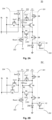
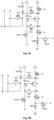
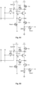
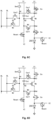
- Figs. 5A to 5D illustrate schematic diagrams of principles of the pixel circuit shown in Fig. 2A in various time periods respectively.
- an operation of the pixel circuit 20 as shown in, for example, Fig. 2A in one display period i will be described in detail with reference to Figs. 2A , 3 , 4A , and 5A to 5D .
- a transistor which is turned off in this time period is indicated by a diagonal line in Fig. 5A , for example, in the first time period T1, the first transistor M1, the third transistor M3, the fourth transistor M4, the fifth transistor M5, and the sixth transistor M6 are turned off.
- the seventh transistor M7 is turned on, and a potential at the anode of the light-emitting element becomes Vinit.
- the eighth transistor M8 is turned on, so that the voltage at the second node N2 becomes the low level initial voltage Vinit.
- the driving transistor Md is turned on, and the potential at the anode of the light-emitting element is further reduced to Vinit rapidly, thereby causing the driving sub-circuit to be reset.
- a voltage difference Vc across the capacitor Cst is equal to Vdd-Vinit.
- the read control signal Sc may be set to an active operating level, so that a voltage value V N1 at the first node N1 at this time is written into the read signal line RL, and is transmitted to a processing IC via the RL to analyze the voltage value V N1 at the first node N1.
- a sensing result of the sensing element Sen in a previous display period (i-1) is determined.
- the processing IC may be a driving IC which provides a display signal, such as a gate driver.
- the first time period T1 may be referred to as a "driving sub-circuit reset phase.”
- a second time period T2 in a second time period T2, as shown in Fig. 5B , the first control signal Con1 and the second control signal Con2 are at a low level, and other signals are at a high level.
- the first control signal Con1 is at a low level, and the third transistor M3 and the fourth transistor M4 are turned on.
- the second control signal Con2 is at a low level, and the first transistor M1 is turned on.
- a transistor which is turned off in this time period is indicated by a diagonal line in Fig. 5B , for example, in the second time period T2, the fifth transistor M5, the sixth transistor M6, the seventh transistor M7, and the eighth transistor M8 are turned off.
- the first transistor M1 Since the first transistor M1 is turned on, the data voltage Vdata on the data signal line is applied to the first node N1, and thus the voltage value V N1 at the first node N1 is equal to Vdata.
- the third transistor M3 is turned on, and a source voltage Vs of the driving transistor Md is equal to Vdata.
- the voltage value V N2 at the second terminal of the storage capacitor Cst that is, the second node N2
- Vg is a gate voltage of the driving transistor Md
- Vth is a threshold voltage of the driving transistor Md.
- the second time period T2 may be referred to as a "data writing phase.”
- a third time period T3 as shown in Fig. 5C , the second control signal Con2 is at a low level, and other signals are at a high level.
- the second control signal Con2 is at a low level, and the first transistor M1 is turned on.
- a transistor which is turned off in this time period is indicated by a diagonal line in Fig. 5C .
- the voltage on the read signal line changes from the data voltage Vdata to the reference voltage Vref
- the first transistor M1 is turned on, and the reference voltage Vref on the data signal line is applied to the first node N1.
- the voltage value V N1 at the first node N1 is equal to Vref, which is equivalent to resetting the sensing sub-circuit to provide a reference potential for the sensing result of the sensing element.
- the third time period T3 may be referred to as a "sensing sub-circuit reset phase. "
- a fourth time period T4 the light-emitting control signal Em is at a low level, and other signals are at a high level.
- the light-emitting control signal Em is at a low level, the fifth transistor M5 and the sixth transistor M6 are turned on, and the light-emitting element emits light.
- a transistor which is turned off in this time period is indicated by a diagonal line in Fig. 5D .
- K is a current constant associated with the driving transistor Md, which is related to process parameters and geometric dimensions of the driving transistor Md.
- the potential V N1 at the first node N1 is equal to Vsense+Vref, where Vsense indicates a value of an external input sensed by the sensing element Sen.
- the read control signal Sc may be set to an active operating level, so that the voltage value V N1 at the first node N1 at this time is written into the read signal line RL, and is transmitted to the processing IC via the RL to analyze the voltage value V N1 at the first node N1, so as to determine the sensing result of the sensing element Sen in the current display period i.
- the sensing element Sen is a piezoelectric ceramic
- the potential at the first node N1 changes (from the reference voltage Vref), and in the fourth time period T4 and/or in a first time period T1 of a next display period (i+1), the potential at the first node N1 is sampeld and transmitted to a processing apparatus via the read signal line RL.
- the processing apparatus performs calculation to confirm the touch at the point and a pressure change at the point.
- the sensing element Sen is a capacitor, for example, a capacitor formed by SD (having a Ti/Al/Ti sandwich structure) metal and gate metal, wherein the Gate metal is generally used as a gate of the TFT, and the SD is generally in contact with a source and a drain of the TFT, in a case where touch is performed by a finger at the point, the potential at the first node N1 changes (from the reference voltage Vref), and in the fourth time period T4 and/or in the first time period T1 of the next display period (i+1), the potential at the first node N1 is sampled and transmitted to the processing apparatus via the read signal line RL.
- the processing apparatus performs caclulation to confirm the touch at the point.
- the sensing element Sen is a photosensor, for example, a photodiode
- the photodiode is turned on, so that the potential at the first node N1 becomes Vdd, or is significantly different from Vref.
- the photosensor may receive light which is diffusely reflected by the finger, so as to determine the touch of the finger or a fingerprint change of the finger, and thereby feed back the change to the processing apparatus.
- the processing apparatus performs calculation to perform image processing such as fingerprint recognition.
- the sensing element Sen is a temperature sensor, for example, a temperature sensitive diode
- the sensing element Sen senses a temperature change
- the potential at the first node N1 changes from Vref, so as to determine a temperature change in an external environment.
- the temperature change may be sensed by the sensing element Sen, and when the sensing element Sen senses that the temperature is too high, the data voltage Vdata may be appropriately reduced by calculation, thereby obtaining a better screen display effect and extending the lifetime of the OLED.
- the sensing element Sen may also be a UltraViolet (UV) sensor or other wavelength sensors.
- the brightness of the screen may be adjuted by sensing external illumination, so as to improve the visual effect.
- the read control signal Sc is at an active operating level in both the first time period T1 and the fourth time period T4
- the read control signal Sc may be set to be at an active operating level in at lest one of the first time period and the fourth time period, so that the sensing voltage sensed by the sensing element is read by the sensing sub-circuit into the read signal line.
- V N1 transmitted to the read control line RL in the first time period T1 substantially indicates the sensing result of the sensing element Sen in a previous display period (i-1)
- V N1 transmitted to the read control line RL in the fourth time period T4 substantially indicates the sensing result of the sensing element Sen in the current display period i.
- a waveform and a frequency of the read control signal Sc in the example of Fig. 4A are merely examples, and the waveform and the frequency of the read control signal Sc may be set to other forms as long as the voltage at the first node N1 may be read into the read signal line in a predetermined time period.
- Figs. 6A to 6D illustrate schematic diagrams of principles of the pixel circuit shown in Fig. 2B in various time periods respectively. It should be illustrated that an operation of the pixel circuit 20' according to the embodiment of the present disclosure as shown in, for example, Fig. 2B in one display period i will be described in detail below with reference to Figs. 2B , 3 and 6A to 6D .
- the sensing sub-circuit of the pixel circuit 20' may further comprise a second transistor M2, wherein a gate of the second transistor is connected to the read control signal terminal, a first electrode of the second transistor is connected to the read signal line RL, and a second electrode of the second transistor is connected to the first node.
- the same technical contents as those in the embodiments described with reference to Figs. 2A and 5A to 5D will not be described in detail again.
- the reset signal Reset may be input to the read control signal terminal SC, that is, the reset signal Reset is used as the read control signal Sc.
- the reset signal Reset (the read control signal Sc) is at a low level, and other signals are at a high level.
- the reset signal Reset is at a low level, and the seventh transistor M7 and the eighth transistor M8 are turned on.
- the read control signal Sc is at a low level, and the second transistor M2 is turned on.
- a potential at the anode of the light-emitting element becomes the low level intial voltage Vinit, and the voltage at the second node N2 becomes the low level initial voltage Vinit.
- the driving transistor Md is turned on, and the potential at the anode of the light-emitting element is further reduced to Vinit rapidly.
- a voltage difference Vc across the capacitor Cst is equal to Vdd-Vinit.
- the second transistor M2 is turned on, so that a voltage value V N1 at the first node N1 at this time is written into the read signal line RL, and is transmitted to a processing IC via the RL to analyze the voltage value V N1 at the first node N1.
- a sensing result of the sensing element Sen in a previous display period (i-1) is determined.
- the first time period T1' may be referred to as a "driving sub-circuit reset phase.”
- a second time period T2' as shown in Fig. 6B , the first control signal Con1 and the second control signal Con2 are at a low level, and other signals are at a high level.
- the third transistor M3 and the fourth transistor M4 are turned on, and the first transistor M1 is turned on.
- the second transistor M2, the fifth transistor M5, the sixth transistor M6, the seventh transistor M7, and the eighth transistor M8 are turned off.
- the second control signal Con2 is at a low level, and other signals are at a high level.
- the second control signal Con2 is at a low level, and the first transistor M1 is turned on.
- the voltage value V N1 at the first node N1 is euqal to Vref, which is equivalent to resetting the sensing sub-circuit to provide a reference potential for the sensing result of the sensing element.
- a fourth time period T4' as shown in Fig. 6D , the light-emitting control signal Em is at a low level, and other signals are at a high level.
- the fifth transistor M5 and the sixth transistor M6 are turned on, and the light-emitting element emits light.
- the potential V N1 at the first node N1 is equal to Vsense+Vref, where Vsense indicates a value of an external input sensed by the sensing element Sen.
- the circuit control and the circuit structure may be simplified by disposing the second transistor M2 and inputting the reset signal Reset to the gate of the second transistor to use the reset signal Reset as the read control signal Sc.
- voltages of all signals are at, for example, a high level to turn off all the transistors. That is, in the buffering time periods, the pixel circuit does not operate, thereby avoiding timing disorder of the pixel circuit. This is because in practical applications, "high level” and “low level” are relatively high and low, and there may be a certain rising time and a certain falling time of a waveform.
- the first control signal Con1 should be at a low level when the reset signal Reset is at a high level.
- the timing disorder may occur. This can be avoided by inserting the buffering periods between the respective time periods.
- a display panel there is provided a display panel.
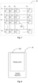
- Fig. 7 illustrates a schematic block diagram of a display panel 70 according to an embodiment of the present disclosure.
- the display panel 70 may comprise a plurality of scanning signal lines SL 1 to SL N ; a plurality of data signal lines DL 1 to DLx disposed to intersect the plurality of scanning signal lines SL 1 to SL N in vertical and horizontal directions; and a plurality of pixel units 700 at intersections of the signal lines and the data signal lines, wherein at least one of the plurality of pixel units 700 is provided with the pixel circuit according to the embodiment of the present disclosure.
- At least one of the plurality of scanning signal lines is used as the read signal line RL.
- the pixel circuit having a sensing element may be regionally arranged according to practical use, layout, and sensing accuracy.
- the sensors may be arranged reasonably, to realize real feedback of screen information (uniformity of screen brightness) and accurately determine a brightness difference, so as to compensate for the screen brightness.
- the sensing element may sense a pressure, a brightness difference, touch of a finger, etc.
- a plurality of sensing elements for sensing a pressure, touch, brightness, and temperature, etc. may be disposed in the display panel in a mixed manner to enable the display panel to have various functions integrated therein.
- a display apparatus According to another aspect of the embodiments of the present disclosure, there is provided a display apparatus.
- Fig. 8 illustrates a schematic block diagram of a display apparatus according to an embodiment of the present disclosure.
- the display apparatus 80 may comprise a display panel 800 according to an embodiment of the present disclosure.
- the display apparatus 80 according to the embodiment of the present disclosure may be any product or component having a display function such as an electronic paper, a mobile phone, a tablet computer, a television, a display, a notebook computer, a digital photo frame, a navigator, etc.
Landscapes
- Engineering & Computer Science (AREA)
- Physics & Mathematics (AREA)
- Computer Hardware Design (AREA)
- General Physics & Mathematics (AREA)
- Theoretical Computer Science (AREA)
- Control Of Indicators Other Than Cathode Ray Tubes (AREA)
- Control Of El Displays (AREA)
Claims (9)
- Circuit de pixels (10, 20, 20'), caractérisé en ce que, comprenant :un élément électroluminescent (105, 205) ;un sous-circuit de commande (101, 201) ayant une borne de commande électroluminescente (EM) pour recevoir un signal de commande électroluminescent (Em) et une borne de sortie connectée à une première borne de l'élément électroluminescent (105, 205), dans lequel le sous-circuit de commande (101, 201) est configuré pour fournir un courant pour amener l'élément électroluminescent (105, 205) à émettre de la lumière vers l'élément électroluminescent (105, 205) sous la commande d'un signal de commande d'émission de lumière (Em) ;un sous-circuit de réinitialisation (102, 202) ayant une borne de signal de réinitialisation (RESET) pour recevoir un signal de réinitialisation (Reset), dans lequel le sous-circuit de réinitialisation (102, 202) est connecté au sous-circuit de commande (101, 201) et à la première borne de l'élément électroluminescent (105, 205), et est configuré pour réinitialiser le sous-circuit de commande (101, 201) et la première borne de l'élément électroluminescent (105, 205) sous la commande du signal de réinitialisation (Reset) ;un sous-circuit d'écriture de données (103, 203) ayant une première borne de signal de commande (CON1) pour recevoir un premier signal de commande (Con1), dans lequel le sous-circuit d'écriture de données (103, 203) est connecté au sous-circuit de commande (101, 201) et au sous-circuit de réinitialisation (102, 202), et est configuré pour écrire une tension de données dans le sous-circuit de commande (101, 201) sous la commande du premier signal de commande (Con1) ; etun sous-circuit de détection (104, 204, 204') ayant une première borne de signal connectée à une ligne de signal de données (DL), une seconde borne de signal connectée à une ligne de signal de lecture (RL), et une seconde borne de signal de commande (CON2) pour recevoir un second signal de commande (Con2), dans lequel le sous-circuit de détection (104, 204, 204') est connecté au sous-circuit d'écriture de données (103, 203),dans lequel le sous-circuit de détection (104, 204, 204') est configuré pour : recevoir un signal de données via la première borne de signal, et transmettre le signal de données au sous-circuit d'écriture de données (103, 203) sous la commande du second signal de commande (Con2) ; et détecter une entrée externe, et lire l'entrée externe détectée dans la ligne de signal de lecture (RL) sous la commande d'un signal de commande de lecture (Sc), dans lequel au moins l'une d'une pluralité de lignes de signal de balayage (SL1, SL2, SL3, SLN) d'un panneau d'affichage est utilisée comme ligne de signal de lecture (RL),le sous-circuit de détection (104, 204, 204') comprend :un élément de détection (Sen), dans lequel une première borne de l'élément de détection (Sen) est connectée à une première borne de tension (V1), et une seconde borne de l'élément de détection (Sen) est connectée à un premier noeud (N1) ; etun premier transistor (M1), dans lequel une grille du premier transistor (M1) est connectée à la seconde borne de signal de commande (CON2), une première électrode du premier transistor (M1) est connectée à la ligne de signal de données (DL), et une seconde électrode du premier transistor (M1) est connectée au premier noeud (N1) ;un deuxième transistor (M2), dans lequel une grille du deuxième transistor (M2) est connectée à la borne de signal de commande de lecture (SC), une première électrode du deuxième transistor (M2) est connectée à la ligne de signal de lecture (RL), et une seconde électrode du deuxième transistor (M2) est connectée au premier noeud (N1),le sous-circuit d'écriture de données (103, 203) comprend :un troisième transistor (M3), dans lequel une grille du troisième transistor (M3) est connectée à la première borne de signal de commande (CON1), une première électrode du troisième transistor (M3) est connectée à un premier noeud (N1), et une seconde électrode du troisième transistor (M3) est connectée au sous-circuit de commande (101, 201) ; etun quatrième transistor (M4), dans lequel une grille du quatrième transistor (M4) est connectée à la première borne de signal de commande (CON1), une première électrode du quatrième transistor (M4) est connectée à un second noeud (N2), et une seconde électrode du quatrième transistor (M4) est connectée au sous-circuit de commande (101, 201),le sous-circuit de commande (101, 201) comprend un cinquième transistor (M5), un condensateur de stockage (Cst), un transistor de commande (Md) et un sixième transistor (M6), dans lequel
une grille du cinquième transistor (M5) est connectée à une borne de signal de commande d'émission de lumière (EM), une première électrode du cinquième transistor (M5) est connectée à une première borne de tension (V1), et une seconde électrode du cinquième transistor (M5) est connecté à une source du transistor de commande (Md) ;une première borne du condensateur de stockage (Cst) est connectée à la première borne de tension (V1), et à une seconde borne du condensateur de stockage (Cst) est connectée à une grille du transistor de commande (Md) ;un drain du transistor de commande (Md) est connecté à une première électrode du sixième transistor (M6) et à la seconde électrode du quatrième transistor (M4), la source du transistor de commande (Md) est connectée à la seconde électrode du troisième transistor (M3), et la grille du transistor de commande (Md) est connectée au second noeud (N2) ; etune grille du sixième transistor (M6) est connectée à la borne de signal de commande électroluminescente (EM), et une seconde électrode du sixième transistor (M6) est connectée à la première borne de l'élément électroluminescent (105, 205), etle sous-circuit de réinitialisation (102, 202) comprend un septième transistor (M7) et un huitième transistor (M8), dans lequel
une grille du huitième transistor (M8) est connectée à la borne de signal de réinitialisation (RESET), une première électrode du huitième transistor (M8) est connectée à une seconde borne de tension (V2), et une seconde électrode du huitième transistor (M8) est connecté à la première électrode du quatrième transistor (M4) ; etune grille du septième transistor (M7) est connectée à la borne de signal de réinitialisation (RESET), une première électrode du septième transistor (M7) est connectée à la seconde borne de tension (V2), et une seconde électrode du septième transistor (M7) est connectée à la première borne de l'élément électroluminescent (105, 205) ; etune seconde borne de l'élément électroluminescent (105, 205) est mise à la masse. - Circuit de pixel (10, 20, 20') selon la revendication 1, dans lequel le sous-circuit de détection (104, 204, 204') comprend en outre une borne de signal de commande de lecture (SC) pour recevoir le signal de commande de lecture (Sc).
- Circuit de pixel (10, 20, 20') selon la revendication 1, dans lequel l'élément de détection (Sen) comprend au moins l'un d'un capteur de pression, d'un photocapteur et d'un capteur de température.
- Panneau d'affichage (70, 800), caractérisé en ce que, comprenant :une pluralité de lignes de signal de balayage (SL1, SL2, SL3, SLN) ;une pluralité de lignes de signal de données (DL1, DL2, DL3, DLN) disposées pour croiser la pluralité de lignes de signal de balayage (SL1, SL2, SL3, SLN) ; etune pluralité d'unités de pixel (700) disposées aux intersections des lignes de signal de données (DL1, DL2, DL3, DLN) et des lignes de signal de balayage (SL1, SL2, SL3, SLN),dans lequel au moins l'une de la pluralité d'unités de pixel (700) comprend le circuit de pixel (10, 20, 20') selon l'une des revendications 1 à 3.
- Appareil d'affichage (80), comprenant le panneau d'affichage (70, 800) selon la revendication 4.
- Procédé (300) pour piloter le circuit de pixel (10, 20, 20') selon l'une des revendications 1 à 3, comprenant :dans une première période de temps, la réinitialisation (S301) du sous-circuit de commande (101, 201) ;dans une deuxième période de temps, l'écriture (S302), par le sous-circuit d'écriture, d'une tension de données dans le sous-circuit de commande (101, 201) ;dans une troisième période de temps, la réinitialisation (S303) du sous-circuit de détection (104, 204, 204') ; etdans une quatrième période de temps, la détection (S304), par le sous-circuit de détection (104, 204, 204'), d'une entrée externe.
- Procédé (300) selon la revendication 6, dans lequel le sous-circuit de détection (104, 204, 204') lit une tension de détection détectée par l'élément de détection (Sen) dans la ligne de signal de lecture (RL) dans au moins l'une des première et quatrième période de temps sous la commande du signal de commande de lecture (Sc).
- Procédé (300) selon la revendication 6, dans lequel dans la première période de temps, le premier transistor (M1) est bloqué et une tension au niveau du premier noeud (N1) est transmise à la ligne de signal de lecture (RL) sous la commande du signal de commande de lecture (Sc) ;dans la deuxième période de temps, la tension sur la ligne de signal de données (DL) est une tension de données, le premier transistor (M1) est activé et le premier noeud (N1) est réglé sur la tension de données ; dans la troisième période de temps, la tension sur la ligne de signal de données (DL) est une tension de référence, le premier transistor (M1) est activé et le premier noeud (N1) est réglé sur la tension de référence ; etdans la quatrième période de temps, le premier transistor (M1) est bloqué, et le premier noeud (N1) est réglé sur une somme de la tension de référence et de la tension de détection.
- Procédé (300) selon la revendication 6, dans lequel le signal de réinitialisation (Reset) est utilisé en tant que signal de commande de lecture (Sc).
Applications Claiming Priority (2)
| Application Number | Priority Date | Filing Date | Title |
|---|---|---|---|
| CN201711231948.8A CN109841189B (zh) | 2017-11-29 | 2017-11-29 | 像素电路及其驱动方法、显示面板和显示装置 |
| PCT/CN2018/107041 WO2019105118A1 (fr) | 2017-11-29 | 2018-09-21 | Circuit de pixel et son procédé de pilotage, et panneau d'affichage et appareil d'affichage |
Publications (3)
| Publication Number | Publication Date |
|---|---|
| EP3719786A1 EP3719786A1 (fr) | 2020-10-07 |
| EP3719786A4 EP3719786A4 (fr) | 2021-06-16 |
| EP3719786B1 true EP3719786B1 (fr) | 2023-09-20 |
Family
ID=66663784
Family Applications (1)
| Application Number | Title | Priority Date | Filing Date |
|---|---|---|---|
| EP18855189.9A Active EP3719786B1 (fr) | 2017-11-29 | 2018-09-21 | Circuit de pixel et son procédé de pilotage, et panneau d'affichage et appareil d'affichage |
Country Status (4)
| Country | Link |
|---|---|
| US (1) | US11367389B2 (fr) |
| EP (1) | EP3719786B1 (fr) |
| CN (1) | CN109841189B (fr) |
| WO (1) | WO2019105118A1 (fr) |
Families Citing this family (9)
| Publication number | Priority date | Publication date | Assignee | Title |
|---|---|---|---|---|
| CN110444158B (zh) | 2019-08-19 | 2021-02-02 | 京东方科技集团股份有限公司 | 像素驱动电路及其驱动方法、显示面板及显示装置 |
| JP2021071593A (ja) * | 2019-10-30 | 2021-05-06 | キヤノン株式会社 | 表示装置、情報表示装置、及び電子機器 |
| US11609657B2 (en) * | 2020-05-07 | 2023-03-21 | Novatek Microelectronics Corp. | Method for driving touch-and-display device, driving circuit, and touch-and-display device |
| CN114323089B (zh) * | 2020-10-12 | 2025-02-25 | 群创光电股份有限公司 | 光检测元件 |
| CN112951153B (zh) * | 2021-02-26 | 2022-09-16 | 京东方科技集团股份有限公司 | 像素电路及其驱动方法、显示面板和显示装置 |
| CN113342212B (zh) * | 2021-07-02 | 2023-03-21 | 业成科技(成都)有限公司 | 触控显示模组及其驱动方法、电子设备 |
| KR20230148891A (ko) | 2022-04-18 | 2023-10-26 | 삼성디스플레이 주식회사 | 화소 및 이를 포함하는 표시 장치 |
| KR20230148892A (ko) * | 2022-04-18 | 2023-10-26 | 삼성디스플레이 주식회사 | 화소 및 이를 포함하는 표시 장치 |
| CN115394254B (zh) * | 2022-10-08 | 2026-02-17 | 北京京东方技术开发有限公司 | 像素电路、驱动方法、显示面板及显示装置 |
Citations (1)
| Publication number | Priority date | Publication date | Assignee | Title |
|---|---|---|---|---|
| US20140292827A1 (en) * | 2013-04-01 | 2014-10-02 | Samsung Display Co., Ltd. | Organic light-emitting display device, method of repairing the same, and method of driving the same |
Family Cites Families (27)
| Publication number | Priority date | Publication date | Assignee | Title |
|---|---|---|---|---|
| GB0318613D0 (en) | 2003-08-08 | 2003-09-10 | Koninkl Philips Electronics Nv | Electroluminescent display devices |
| WO2008065584A1 (fr) * | 2006-11-28 | 2008-06-05 | Koninklijke Philips Electronics N.V. | Dispositif d'affichage à matrice active à rétroaction optique et procédé de commande de celui-ci |
| KR101073353B1 (ko) * | 2009-10-19 | 2011-10-14 | 삼성모바일디스플레이주식회사 | 화소 및 그를 이용한 유기전계발광표시장치 |
| KR101991099B1 (ko) * | 2012-03-29 | 2019-06-20 | 삼성디스플레이 주식회사 | 화소 및 그 화소 어레이의 시험 방법 |
| KR102023598B1 (ko) * | 2012-11-20 | 2019-09-23 | 삼성디스플레이 주식회사 | 화소, 이를 포함하는 표시장치 및 그 구동 방법 |
| KR102012759B1 (ko) * | 2012-11-23 | 2019-08-22 | 삼성디스플레이 주식회사 | 유기 발광 표시 장치 및 그 구동 방법 |
| KR102046442B1 (ko) * | 2013-05-09 | 2019-11-20 | 삼성디스플레이 주식회사 | 유기 발광 표시 장치 |
| CN203311812U (zh) | 2013-05-30 | 2013-11-27 | 京东方科技集团股份有限公司 | 一种触摸显示驱动电路和显示装置 |
| CN103325339B (zh) | 2013-06-21 | 2016-05-25 | 京东方科技集团股份有限公司 | 像素电路及其驱动方法、有机发光显示面板及显示装置 |
| CN103383837B (zh) * | 2013-07-09 | 2015-07-01 | 京东方科技集团股份有限公司 | 一种触摸显示驱动电路、驱动方法及显示装置 |
| KR102151751B1 (ko) * | 2013-07-19 | 2020-10-27 | 삼성디스플레이 주식회사 | 박막 트랜지스터 어레이 기판 및 이를 포함하는 유기 발광 표시 장치 |
| CN203502926U (zh) * | 2013-07-31 | 2014-03-26 | 京东方科技集团股份有限公司 | 有机发光二极管像素电路和显示装置 |
| CN203895093U (zh) * | 2014-05-26 | 2014-10-22 | 京东方科技集团股份有限公司 | 像素电路和显示装置 |
| CN104021756B (zh) | 2014-05-29 | 2017-04-12 | 京东方科技集团股份有限公司 | 像素电路及其驱动方法、有机发光显示面板及显示装置 |
| CN104112120B (zh) | 2014-06-26 | 2018-09-18 | 京东方科技集团股份有限公司 | 指纹识别显示驱动电路和显示装置 |
| CN104091562B (zh) | 2014-06-27 | 2016-01-13 | 京东方科技集团股份有限公司 | 像素电路、显示面板及显示装置 |
| CN104217677B (zh) | 2014-07-30 | 2016-08-24 | 京东方科技集团股份有限公司 | 触控显示电路及显示装置 |
| CN104299571B (zh) * | 2014-11-06 | 2016-07-06 | 合肥鑫晟光电科技有限公司 | 一种像素电路、有机电致发光显示面板及显示装置 |
| CN104778923B (zh) | 2015-04-28 | 2016-06-01 | 京东方科技集团股份有限公司 | 一种像素电路及其驱动方法、显示装置 |
| CN104835449B (zh) * | 2015-05-04 | 2017-05-17 | 京东方科技集团股份有限公司 | 像素电路及其驱动方法、阵列基板以及显示装置 |
| KR102294133B1 (ko) * | 2015-06-15 | 2021-08-27 | 삼성디스플레이 주식회사 | 유기발광 디스플레이 장치의 스캔 드라이버, 유기발광 디스플레이 장치 및 이를 포함하는 디스플레이 시스템 |
| KR102417983B1 (ko) | 2015-08-27 | 2022-07-07 | 삼성디스플레이 주식회사 | 유기전계발광 표시장치 및 그의 구동방법 |
| CN105118438B (zh) | 2015-09-21 | 2017-07-25 | 京东方科技集团股份有限公司 | 像素驱动电路、方法、像素电路和显示装置 |
| CN205122154U (zh) * | 2015-09-21 | 2016-03-30 | 京东方科技集团股份有限公司 | 像素驱动电路、像素电路和显示装置 |
| CN105427803B (zh) | 2016-01-04 | 2018-01-02 | 京东方科技集团股份有限公司 | 像素驱动电路、方法、显示面板和显示装置 |
| CN106531076B (zh) * | 2017-01-12 | 2019-03-01 | 京东方科技集团股份有限公司 | 一种像素电路、显示面板及其驱动方法 |
| CN107358917B (zh) | 2017-08-21 | 2020-04-28 | 上海天马微电子有限公司 | 一种像素电路、其驱动方法、显示面板及显示装置 |
-
2017
- 2017-11-29 CN CN201711231948.8A patent/CN109841189B/zh active Active
-
2018
- 2018-09-21 WO PCT/CN2018/107041 patent/WO2019105118A1/fr not_active Ceased
- 2018-09-21 US US16/335,195 patent/US11367389B2/en active Active
- 2018-09-21 EP EP18855189.9A patent/EP3719786B1/fr active Active
Patent Citations (1)
| Publication number | Priority date | Publication date | Assignee | Title |
|---|---|---|---|---|
| US20140292827A1 (en) * | 2013-04-01 | 2014-10-02 | Samsung Display Co., Ltd. | Organic light-emitting display device, method of repairing the same, and method of driving the same |
Also Published As
| Publication number | Publication date |
|---|---|
| US20210366382A1 (en) | 2021-11-25 |
| EP3719786A1 (fr) | 2020-10-07 |
| WO2019105118A1 (fr) | 2019-06-06 |
| US11367389B2 (en) | 2022-06-21 |
| EP3719786A4 (fr) | 2021-06-16 |
| CN109841189B (zh) | 2020-08-14 |
| CN109841189A (zh) | 2019-06-04 |
Similar Documents
| Publication | Publication Date | Title |
|---|---|---|
| EP3719786B1 (fr) | Circuit de pixel et son procédé de pilotage, et panneau d'affichage et appareil d'affichage | |
| US9778800B2 (en) | Pixel circuit, display panel and display apparatus | |
| EP3159882B1 (fr) | Circuit de pixels, procédé pour sa commande et dispositif d'affichage | |
| CN101943974B (zh) | 光敏电路、包括光敏电路的触控板和驱动光敏电路的方法 | |
| US9645662B2 (en) | Pixel circuit, display panel and display apparatus | |
| US10262597B2 (en) | Pixel circuit and driving method thereof, array substrate and display apparatus | |
| CN108628501B (zh) | 适配于触摸感测的电流驱动的显示面板以及面板显示装置 | |
| US10068950B2 (en) | Pixel circuit, driving method thereof, and display apparatus | |
| EP2887344B1 (fr) | Circuit de pilotage d'affichage à commande tactile, procédé de pilotage associé et dispositif d'affichage | |
| CN103996377B (zh) | 像素电路和显示装置 | |
| US11636789B2 (en) | Pixel unit, array substrate, display panel, display apparatus, and detection method of pixel circuit | |
| US11341906B2 (en) | Pixel circuit, method, and AMOLED display with optical touch sensing | |
| US10642389B2 (en) | Touch display driving circuit, touch display apparatus | |
| US9740320B2 (en) | Pixel circuit and display apparatus | |
| KR102070109B1 (ko) | 터치-제어 픽셀-구동 회로 및 그 방법, 터치-제어 디스플레이 장치 | |
| US11081055B2 (en) | Active matrix-based electronic apparatus including a light emitting device that may be non-foward biased to sense light, and method of driving the same |
Legal Events
| Date | Code | Title | Description |
|---|---|---|---|
| STAA | Information on the status of an ep patent application or granted ep patent |
Free format text: STATUS: UNKNOWN |
|
| STAA | Information on the status of an ep patent application or granted ep patent |
Free format text: STATUS: THE INTERNATIONAL PUBLICATION HAS BEEN MADE |
|
| PUAI | Public reference made under article 153(3) epc to a published international application that has entered the european phase |
Free format text: ORIGINAL CODE: 0009012 |
|
| STAA | Information on the status of an ep patent application or granted ep patent |
Free format text: STATUS: REQUEST FOR EXAMINATION WAS MADE |
|
| 17P | Request for examination filed |
Effective date: 20190322 |
|
| AK | Designated contracting states |
Kind code of ref document: A1 Designated state(s): AL AT BE BG CH CY CZ DE DK EE ES FI FR GB GR HR HU IE IS IT LI LT LU LV MC MK MT NL NO PL PT RO RS SE SI SK SM TR |
|
| AX | Request for extension of the european patent |
Extension state: BA ME |
|
| DAV | Request for validation of the european patent (deleted) | ||
| DAX | Request for extension of the european patent (deleted) | ||
| A4 | Supplementary search report drawn up and despatched |
Effective date: 20210517 |
|
| RIC1 | Information provided on ipc code assigned before grant |
Ipc: G09G 3/3225 20160101AFI20210510BHEP Ipc: G09G 3/3233 20160101ALI20210510BHEP Ipc: G06F 3/041 20060101ALI20210510BHEP |
|
| STAA | Information on the status of an ep patent application or granted ep patent |
Free format text: STATUS: EXAMINATION IS IN PROGRESS |
|
| 17Q | First examination report despatched |
Effective date: 20230117 |
|
| GRAP | Despatch of communication of intention to grant a patent |
Free format text: ORIGINAL CODE: EPIDOSNIGR1 |
|
| STAA | Information on the status of an ep patent application or granted ep patent |
Free format text: STATUS: GRANT OF PATENT IS INTENDED |
|
| INTG | Intention to grant announced |
Effective date: 20230428 |
|
| GRAS | Grant fee paid |
Free format text: ORIGINAL CODE: EPIDOSNIGR3 |
|
| GRAA | (expected) grant |
Free format text: ORIGINAL CODE: 0009210 |
|
| STAA | Information on the status of an ep patent application or granted ep patent |
Free format text: STATUS: THE PATENT HAS BEEN GRANTED |
|
| AK | Designated contracting states |
Kind code of ref document: B1 Designated state(s): AL AT BE BG CH CY CZ DE DK EE ES FI FR GB GR HR HU IE IS IT LI LT LU LV MC MK MT NL NO PL PT RO RS SE SI SK SM TR |
|
| REG | Reference to a national code |
Ref country code: GB Ref legal event code: FG4D |
|
| REG | Reference to a national code |
Ref country code: CH Ref legal event code: EP |
|
| REG | Reference to a national code |
Ref country code: IE Ref legal event code: FG4D |
|
| REG | Reference to a national code |
Ref country code: DE Ref legal event code: R096 Ref document number: 602018058037 Country of ref document: DE |
|
| REG | Reference to a national code |
Ref country code: LT Ref legal event code: MG9D |
|
| PG25 | Lapsed in a contracting state [announced via postgrant information from national office to epo] |
Ref country code: GR Free format text: LAPSE BECAUSE OF FAILURE TO SUBMIT A TRANSLATION OF THE DESCRIPTION OR TO PAY THE FEE WITHIN THE PRESCRIBED TIME-LIMIT Effective date: 20231221 |
|
| REG | Reference to a national code |
Ref country code: NL Ref legal event code: MP Effective date: 20230920 |
|
| PG25 | Lapsed in a contracting state [announced via postgrant information from national office to epo] |
Ref country code: SE Free format text: LAPSE BECAUSE OF FAILURE TO SUBMIT A TRANSLATION OF THE DESCRIPTION OR TO PAY THE FEE WITHIN THE PRESCRIBED TIME-LIMIT Effective date: 20230920 Ref country code: RS Free format text: LAPSE BECAUSE OF FAILURE TO SUBMIT A TRANSLATION OF THE DESCRIPTION OR TO PAY THE FEE WITHIN THE PRESCRIBED TIME-LIMIT Effective date: 20230920 Ref country code: NO Free format text: LAPSE BECAUSE OF FAILURE TO SUBMIT A TRANSLATION OF THE DESCRIPTION OR TO PAY THE FEE WITHIN THE PRESCRIBED TIME-LIMIT Effective date: 20231220 Ref country code: LV Free format text: LAPSE BECAUSE OF FAILURE TO SUBMIT A TRANSLATION OF THE DESCRIPTION OR TO PAY THE FEE WITHIN THE PRESCRIBED TIME-LIMIT Effective date: 20230920 Ref country code: LT Free format text: LAPSE BECAUSE OF FAILURE TO SUBMIT A TRANSLATION OF THE DESCRIPTION OR TO PAY THE FEE WITHIN THE PRESCRIBED TIME-LIMIT Effective date: 20230920 Ref country code: HR Free format text: LAPSE BECAUSE OF FAILURE TO SUBMIT A TRANSLATION OF THE DESCRIPTION OR TO PAY THE FEE WITHIN THE PRESCRIBED TIME-LIMIT Effective date: 20230920 Ref country code: GR Free format text: LAPSE BECAUSE OF FAILURE TO SUBMIT A TRANSLATION OF THE DESCRIPTION OR TO PAY THE FEE WITHIN THE PRESCRIBED TIME-LIMIT Effective date: 20231221 Ref country code: FI Free format text: LAPSE BECAUSE OF FAILURE TO SUBMIT A TRANSLATION OF THE DESCRIPTION OR TO PAY THE FEE WITHIN THE PRESCRIBED TIME-LIMIT Effective date: 20230920 |
|
| REG | Reference to a national code |
Ref country code: AT Ref legal event code: MK05 Ref document number: 1614041 Country of ref document: AT Kind code of ref document: T Effective date: 20230920 |
|
| PG25 | Lapsed in a contracting state [announced via postgrant information from national office to epo] |
Ref country code: NL Free format text: LAPSE BECAUSE OF FAILURE TO SUBMIT A TRANSLATION OF THE DESCRIPTION OR TO PAY THE FEE WITHIN THE PRESCRIBED TIME-LIMIT Effective date: 20230920 |
|
| PG25 | Lapsed in a contracting state [announced via postgrant information from national office to epo] |
Ref country code: IS Free format text: LAPSE BECAUSE OF FAILURE TO SUBMIT A TRANSLATION OF THE DESCRIPTION OR TO PAY THE FEE WITHIN THE PRESCRIBED TIME-LIMIT Effective date: 20240120 |
|
| PG25 | Lapsed in a contracting state [announced via postgrant information from national office to epo] |
Ref country code: AT Free format text: LAPSE BECAUSE OF FAILURE TO SUBMIT A TRANSLATION OF THE DESCRIPTION OR TO PAY THE FEE WITHIN THE PRESCRIBED TIME-LIMIT Effective date: 20230920 |
|
| PG25 | Lapsed in a contracting state [announced via postgrant information from national office to epo] |
Ref country code: ES Free format text: LAPSE BECAUSE OF FAILURE TO SUBMIT A TRANSLATION OF THE DESCRIPTION OR TO PAY THE FEE WITHIN THE PRESCRIBED TIME-LIMIT Effective date: 20230920 |
|
| PG25 | Lapsed in a contracting state [announced via postgrant information from national office to epo] |
Ref country code: SM Free format text: LAPSE BECAUSE OF FAILURE TO SUBMIT A TRANSLATION OF THE DESCRIPTION OR TO PAY THE FEE WITHIN THE PRESCRIBED TIME-LIMIT Effective date: 20230920 Ref country code: RO Free format text: LAPSE BECAUSE OF FAILURE TO SUBMIT A TRANSLATION OF THE DESCRIPTION OR TO PAY THE FEE WITHIN THE PRESCRIBED TIME-LIMIT Effective date: 20230920 Ref country code: IS Free format text: LAPSE BECAUSE OF FAILURE TO SUBMIT A TRANSLATION OF THE DESCRIPTION OR TO PAY THE FEE WITHIN THE PRESCRIBED TIME-LIMIT Effective date: 20240120 Ref country code: ES Free format text: LAPSE BECAUSE OF FAILURE TO SUBMIT A TRANSLATION OF THE DESCRIPTION OR TO PAY THE FEE WITHIN THE PRESCRIBED TIME-LIMIT Effective date: 20230920 Ref country code: EE Free format text: LAPSE BECAUSE OF FAILURE TO SUBMIT A TRANSLATION OF THE DESCRIPTION OR TO PAY THE FEE WITHIN THE PRESCRIBED TIME-LIMIT Effective date: 20230920 Ref country code: CZ Free format text: LAPSE BECAUSE OF FAILURE TO SUBMIT A TRANSLATION OF THE DESCRIPTION OR TO PAY THE FEE WITHIN THE PRESCRIBED TIME-LIMIT Effective date: 20230920 Ref country code: AT Free format text: LAPSE BECAUSE OF FAILURE TO SUBMIT A TRANSLATION OF THE DESCRIPTION OR TO PAY THE FEE WITHIN THE PRESCRIBED TIME-LIMIT Effective date: 20230920 Ref country code: SK Free format text: LAPSE BECAUSE OF FAILURE TO SUBMIT A TRANSLATION OF THE DESCRIPTION OR TO PAY THE FEE WITHIN THE PRESCRIBED TIME-LIMIT Effective date: 20230920 Ref country code: PT Free format text: LAPSE BECAUSE OF FAILURE TO SUBMIT A TRANSLATION OF THE DESCRIPTION OR TO PAY THE FEE WITHIN THE PRESCRIBED TIME-LIMIT Effective date: 20240122 |
|
| REG | Reference to a national code |
Ref country code: CH Ref legal event code: PL |
|
| PG25 | Lapsed in a contracting state [announced via postgrant information from national office to epo] |
Ref country code: LU Free format text: LAPSE BECAUSE OF NON-PAYMENT OF DUE FEES Effective date: 20230921 |
|
| REG | Reference to a national code |
Ref country code: BE Ref legal event code: MM Effective date: 20230930 |
|
| PG25 | Lapsed in a contracting state [announced via postgrant information from national office to epo] |
Ref country code: PL Free format text: LAPSE BECAUSE OF FAILURE TO SUBMIT A TRANSLATION OF THE DESCRIPTION OR TO PAY THE FEE WITHIN THE PRESCRIBED TIME-LIMIT Effective date: 20230920 Ref country code: LU Free format text: LAPSE BECAUSE OF NON-PAYMENT OF DUE FEES Effective date: 20230921 Ref country code: IT Free format text: LAPSE BECAUSE OF FAILURE TO SUBMIT A TRANSLATION OF THE DESCRIPTION OR TO PAY THE FEE WITHIN THE PRESCRIBED TIME-LIMIT Effective date: 20230920 |
|
| REG | Reference to a national code |
Ref country code: DE Ref legal event code: R097 Ref document number: 602018058037 Country of ref document: DE |
|
| PG25 | Lapsed in a contracting state [announced via postgrant information from national office to epo] |
Ref country code: MC Free format text: LAPSE BECAUSE OF FAILURE TO SUBMIT A TRANSLATION OF THE DESCRIPTION OR TO PAY THE FEE WITHIN THE PRESCRIBED TIME-LIMIT Effective date: 20230920 |
|
| REG | Reference to a national code |
Ref country code: IE Ref legal event code: MM4A |
|
| PG25 | Lapsed in a contracting state [announced via postgrant information from national office to epo] |
Ref country code: IE Free format text: LAPSE BECAUSE OF NON-PAYMENT OF DUE FEES Effective date: 20230921 |
|
| PG25 | Lapsed in a contracting state [announced via postgrant information from national office to epo] |
Ref country code: DK Free format text: LAPSE BECAUSE OF FAILURE TO SUBMIT A TRANSLATION OF THE DESCRIPTION OR TO PAY THE FEE WITHIN THE PRESCRIBED TIME-LIMIT Effective date: 20230920 |
|
| PG25 | Lapsed in a contracting state [announced via postgrant information from national office to epo] |
Ref country code: CH Free format text: LAPSE BECAUSE OF NON-PAYMENT OF DUE FEES Effective date: 20230930 |
|
| PLBE | No opposition filed within time limit |
Free format text: ORIGINAL CODE: 0009261 |
|
| STAA | Information on the status of an ep patent application or granted ep patent |
Free format text: STATUS: NO OPPOSITION FILED WITHIN TIME LIMIT |
|
| PG25 | Lapsed in a contracting state [announced via postgrant information from national office to epo] |
Ref country code: MC Free format text: LAPSE BECAUSE OF FAILURE TO SUBMIT A TRANSLATION OF THE DESCRIPTION OR TO PAY THE FEE WITHIN THE PRESCRIBED TIME-LIMIT Effective date: 20230920 Ref country code: IE Free format text: LAPSE BECAUSE OF NON-PAYMENT OF DUE FEES Effective date: 20230921 Ref country code: DK Free format text: LAPSE BECAUSE OF FAILURE TO SUBMIT A TRANSLATION OF THE DESCRIPTION OR TO PAY THE FEE WITHIN THE PRESCRIBED TIME-LIMIT Effective date: 20230920 Ref country code: CH Free format text: LAPSE BECAUSE OF NON-PAYMENT OF DUE FEES Effective date: 20230930 |
|
| 26N | No opposition filed |
Effective date: 20240621 |
|
| GBPC | Gb: european patent ceased through non-payment of renewal fee |
Effective date: 20231220 |
|
| PG25 | Lapsed in a contracting state [announced via postgrant information from national office to epo] |
Ref country code: BE Free format text: LAPSE BECAUSE OF NON-PAYMENT OF DUE FEES Effective date: 20230930 |
|
| PGFP | Annual fee paid to national office [announced via postgrant information from national office to epo] |
Ref country code: DE Payment date: 20240918 Year of fee payment: 7 |
|
| PG25 | Lapsed in a contracting state [announced via postgrant information from national office to epo] |
Ref country code: GB Free format text: LAPSE BECAUSE OF NON-PAYMENT OF DUE FEES Effective date: 20231220 |
|
| PG25 | Lapsed in a contracting state [announced via postgrant information from national office to epo] |
Ref country code: FR Free format text: LAPSE BECAUSE OF NON-PAYMENT OF DUE FEES Effective date: 20231120 |
|
| PG25 | Lapsed in a contracting state [announced via postgrant information from national office to epo] |
Ref country code: SI Free format text: LAPSE BECAUSE OF FAILURE TO SUBMIT A TRANSLATION OF THE DESCRIPTION OR TO PAY THE FEE WITHIN THE PRESCRIBED TIME-LIMIT Effective date: 20230920 |
|
| PG25 | Lapsed in a contracting state [announced via postgrant information from national office to epo] |
Ref country code: SI Free format text: LAPSE BECAUSE OF FAILURE TO SUBMIT A TRANSLATION OF THE DESCRIPTION OR TO PAY THE FEE WITHIN THE PRESCRIBED TIME-LIMIT Effective date: 20230920 Ref country code: GB Free format text: LAPSE BECAUSE OF NON-PAYMENT OF DUE FEES Effective date: 20231220 Ref country code: FR Free format text: LAPSE BECAUSE OF NON-PAYMENT OF DUE FEES Effective date: 20231120 |
|
| PG25 | Lapsed in a contracting state [announced via postgrant information from national office to epo] |
Ref country code: BG Free format text: LAPSE BECAUSE OF FAILURE TO SUBMIT A TRANSLATION OF THE DESCRIPTION OR TO PAY THE FEE WITHIN THE PRESCRIBED TIME-LIMIT Effective date: 20230920 |
|
| PG25 | Lapsed in a contracting state [announced via postgrant information from national office to epo] |
Ref country code: BG Free format text: LAPSE BECAUSE OF FAILURE TO SUBMIT A TRANSLATION OF THE DESCRIPTION OR TO PAY THE FEE WITHIN THE PRESCRIBED TIME-LIMIT Effective date: 20230920 |
|
| PG25 | Lapsed in a contracting state [announced via postgrant information from national office to epo] |
Ref country code: CY Free format text: LAPSE BECAUSE OF FAILURE TO SUBMIT A TRANSLATION OF THE DESCRIPTION OR TO PAY THE FEE WITHIN THE PRESCRIBED TIME-LIMIT; INVALID AB INITIO Effective date: 20180921 |
|
| PG25 | Lapsed in a contracting state [announced via postgrant information from national office to epo] |
Ref country code: HU Free format text: LAPSE BECAUSE OF FAILURE TO SUBMIT A TRANSLATION OF THE DESCRIPTION OR TO PAY THE FEE WITHIN THE PRESCRIBED TIME-LIMIT; INVALID AB INITIO Effective date: 20180921 |
|
| PG25 | Lapsed in a contracting state [announced via postgrant information from national office to epo] |
Ref country code: TR Free format text: LAPSE BECAUSE OF FAILURE TO SUBMIT A TRANSLATION OF THE DESCRIPTION OR TO PAY THE FEE WITHIN THE PRESCRIBED TIME-LIMIT Effective date: 20230920 |