EP3719997A1 - Circuit d'un commutateur à semi-conducteur - Google Patents
Circuit d'un commutateur à semi-conducteur Download PDFInfo
- Publication number
- EP3719997A1 EP3719997A1 EP19166563.7A EP19166563A EP3719997A1 EP 3719997 A1 EP3719997 A1 EP 3719997A1 EP 19166563 A EP19166563 A EP 19166563A EP 3719997 A1 EP3719997 A1 EP 3719997A1
- Authority
- EP
- European Patent Office
- Prior art keywords
- gate
- diode
- circuit
- resistor
- capacitor
- Prior art date
- Legal status (The legal status is an assumption and is not a legal conclusion. Google has not performed a legal analysis and makes no representation as to the accuracy of the status listed.)
- Withdrawn
Links
- 239000004065 semiconductor Substances 0.000 title claims abstract description 40
- 239000003990 capacitor Substances 0.000 claims abstract description 43
- 230000005669 field effect Effects 0.000 description 2
- 230000001105 regulatory effect Effects 0.000 description 2
- 230000006978 adaptation Effects 0.000 description 1
- 238000001816 cooling Methods 0.000 description 1
- 230000000694 effects Effects 0.000 description 1
- 238000000034 method Methods 0.000 description 1
- 238000004804 winding Methods 0.000 description 1
Images


Classifications
-
- H—ELECTRICITY
- H03—ELECTRONIC CIRCUITRY
- H03K—PULSE TECHNIQUE
- H03K17/00—Electronic switching or gating, i.e. not by contact-making and –breaking
- H03K17/16—Modifications for eliminating interference voltages or currents
- H03K17/161—Modifications for eliminating interference voltages or currents in field-effect transistor switches
- H03K17/165—Modifications for eliminating interference voltages or currents in field-effect transistor switches by feedback from the output circuit to the control circuit
- H03K17/166—Soft switching
-
- H—ELECTRICITY
- H03—ELECTRONIC CIRCUITRY
- H03K—PULSE TECHNIQUE
- H03K17/00—Electronic switching or gating, i.e. not by contact-making and –breaking
- H03K17/16—Modifications for eliminating interference voltages or currents
- H03K17/168—Modifications for eliminating interference voltages or currents in composite switches
-
- H—ELECTRICITY
- H03—ELECTRONIC CIRCUITRY
- H03K—PULSE TECHNIQUE
- H03K17/00—Electronic switching or gating, i.e. not by contact-making and –breaking
- H03K17/51—Electronic switching or gating, i.e. not by contact-making and –breaking characterised by the components used
- H03K17/56—Electronic switching or gating, i.e. not by contact-making and –breaking characterised by the components used by the use, as active elements, of semiconductor devices
- H03K17/567—Circuits characterised by the use of more than one type of semiconductor device, e.g. BIMOS, composite devices such as IGBT
-
- H—ELECTRICITY
- H03—ELECTRONIC CIRCUITRY
- H03K—PULSE TECHNIQUE
- H03K17/00—Electronic switching or gating, i.e. not by contact-making and –breaking
- H03K17/51—Electronic switching or gating, i.e. not by contact-making and –breaking characterised by the components used
- H03K17/74—Electronic switching or gating, i.e. not by contact-making and –breaking characterised by the components used by the use, as active elements, of diodes
-
- H—ELECTRICITY
- H03—ELECTRONIC CIRCUITRY
- H03K—PULSE TECHNIQUE
- H03K17/00—Electronic switching or gating, i.e. not by contact-making and –breaking
- H03K17/04—Modifications for accelerating switching
- H03K17/0406—Modifications for accelerating switching in composite switches
-
- H—ELECTRICITY
- H03—ELECTRONIC CIRCUITRY
- H03K—PULSE TECHNIQUE
- H03K17/00—Electronic switching or gating, i.e. not by contact-making and –breaking
- H03K17/04—Modifications for accelerating switching
- H03K17/042—Modifications for accelerating switching by feedback from the output circuit to the control circuit
- H03K17/04206—Modifications for accelerating switching by feedback from the output circuit to the control circuit in field-effect transistor switches
-
- H—ELECTRICITY
- H03—ELECTRONIC CIRCUITRY
- H03K—PULSE TECHNIQUE
- H03K17/00—Electronic switching or gating, i.e. not by contact-making and –breaking
- H03K17/08—Modifications for protecting switching circuit against overcurrent or overvoltage
- H03K17/082—Modifications for protecting switching circuit against overcurrent or overvoltage by feedback from the output to the control circuit
- H03K17/0822—Modifications for protecting switching circuit against overcurrent or overvoltage by feedback from the output to the control circuit in field-effect transistor switches
-
- H—ELECTRICITY
- H03—ELECTRONIC CIRCUITRY
- H03K—PULSE TECHNIQUE
- H03K17/00—Electronic switching or gating, i.e. not by contact-making and –breaking
- H03K17/08—Modifications for protecting switching circuit against overcurrent or overvoltage
- H03K17/082—Modifications for protecting switching circuit against overcurrent or overvoltage by feedback from the output to the control circuit
- H03K17/0828—Modifications for protecting switching circuit against overcurrent or overvoltage by feedback from the output to the control circuit in composite switches
Definitions
- the invention relates to a circuit for a semiconductor switch.
- the gate resistor is adjusted to set the maximum voltage gradient. If the maximum voltage rise is limited by the gate resistor, the average voltage rise also slows down. Slower switching operations lead to increased switching losses in the semiconductor switch, which has a negative effect on the service life of the semiconductor switch and the converter with the same cooling system.
- the aim is to reduce the maximum values of the voltage rate of rise during switching without influencing the average voltage rate of rise, i.e. to linearize the switching edge.
- the voltage edge can be set to a value in a manner that is regulated.
- Switching on and off is influenced to the same extent by the additional capacitance C1.
- an optimal capacitance value for switching on causes the switching process to be slowed down, which must be compensated for with a smaller gate resistance. In most cases, this leads to the same switching edges when switching off, but does not bring any improvement in terms of losses and leads to a higher switch-off overvoltage.
- driver circuits e.g. driver circuit with a regulated current source.
- driver circuits e.g. driver circuit with a regulated current source.
- simple gate driver circuits a compromise is made between switching on and off. An optimal setting is not possible in this case.
- the invention is based on the object of specifying an improved circuit for a semiconductor switch.
- a circuit of a semiconductor switch comprising a gate, a collector or a drain and an emitter or a source
- the circuitry comprising a capacitor between the gate and collector or drain, with one in series with the capacitor Parallel connection of a resistor and a diode is provided.
- the diode is switched away from the gate in the forward direction.
- the switch-on behavior of the semiconductor switch is influenced and / or improved.
- the diode is switched in the forward direction towards the gate.
- the turn-off behavior of the semiconductor switch is influenced and / or improved.
- the diode is switched away from the gate in the forward direction, a further arrangement of a further capacitor, a further resistor and a further diode being connected in parallel to the arrangement of capacitor, resistor and diode, a parallel connection being made in series with the further capacitor the further resistor and the further diode is provided, the further diode being applied in the flow direction towards the gate.
- the on and off behavior of the semiconductor switch is thus influenced and / or improved (independently of one another).
- a further capacitor is connected in parallel to the resistor and the diode.
- a circuit of a semiconductor switch comprising a gate, a collector or a drain and an emitter or a source
- the circuitry comprising a capacitor between gate and collector or drain, with parallel a circuit is provided for the capacitor in which a diode is connected in series to a parallel circuit of a resistor and a further capacitor.
- the diode can be switched away from the gate or towards the gate in the flow direction.
- a gate resistor circuit comprising a first gate resistor connected to the gate, to which a series circuit of a second gate resistor and a gate diode is connected in parallel, the gate diode being connected in such a way that it allows a current to flow to the gate.
- the discharge resistor is connected in parallel with the capacitor or in parallel with the diode.
- the semiconductor switch is designed as an IGBT or a MOSFET.
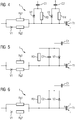
- Figure 1 shows a circuit 1 of a semiconductor switch T1 known from the prior art.
- the semiconductor switch T1 is, for example, a field effect transistor, in particular a MOSFET or an IGBT, and has a gate G, a collector C and an emitter E.
- a capacitor C1 is arranged between collector C and gate G.
- a gate circuit made up of a first gate resistor Rg1, a second gate resistor Rg2 and a gate diode V1 is shown which, as explained above in the introduction, symbolizes the gate resistor.
- Figure 2 shows a first embodiment of a circuit 1 of a semiconductor switch T1.
- the semiconductor switch T1 is, for example, a field effect transistor, in particular a MOSFET or an IGBT, and has a gate G, a collector C and an emitter E.
- a capacitor C1 is arranged between collector C and gate G.
- a gate circuit made up of a first gate resistor Rg1, a second gate resistor Rg2 and a gate diode V1 is shown which, as explained above in the introduction, symbolizes the gate resistor.
- a parallel connection of a resistor R3 and a diode V2 is provided between collector C and gate G in series with capacitor C1, with diode V2 being switched away from gate G in the forward direction.
- the resistor R3 is used to discharge the capacitor C1 if this is not possible due to the diode V2 operating in its reverse direction.
- the orientation of the diode V2 determines whether the circuit 1 is effective when the semiconductor switch T1 is switched on or off.
- Figure 3 shows a second embodiment of a circuit 1 of a semiconductor switch T1.
- the circuit 1 is similar to that in Figure 2 1. In contrast to this, however, the diode V2 is switched in the flow direction towards the gate G.
- the resistor R3 is used to discharge the capacitor C1 if this is not possible due to the diode V2 operating in its reverse direction.
- Figure 4 shows a third embodiment of a circuit 1 of a semiconductor switch T1.
- the circuit 1 combines the in the Figures 2 and 3 circuits shown 1.
- a parallel connection of a resistor R3 and a diode V2 is provided in series with the capacitor C1 between the collector C and the gate G, the diode V2 being switched away from the gate G in the forward direction.
- a further arrangement of a further capacitor C2, a further resistor R4 and a further diode V3 is connected in parallel to the arrangement of capacitor C1, resistor R3 and diode V2, the further capacitor C2 being applied, for example, to the collector C and in series with the further capacitor C2 a parallel connection of the further resistor R4 and the further diode V3 is provided, the further diode V3 being connected in the flow direction towards the gate G.
- the switching on and off behavior is influenced and / or improved separately from one another.
- Figure 5 shows a fourth embodiment of a circuit 1 of a semiconductor switch T1.
- the circuit 1 is similar to that in Figure 3 1. In contrast to this, the resistor R3 and the diode V2 are connected in parallel to a further capacitor C2.
- Figure 6 shows a fifth embodiment of a circuit 1 of a semiconductor switch T1.
- the circuit 1 is similar to that in Figure 2 1. In contrast to this, the resistor R3 and the diode V2 are connected in parallel to a further capacitor C2.
- Figure 7 shows a sixth embodiment of a circuit 1 of a semiconductor switch T1.
- the circuit 1 is similar to that in Figure 1 1.
- a circuit is provided in parallel with the capacitor C1, in which a diode V2 is connected in series with a parallel circuit comprising a resistor R3 and a further capacitor C2.
- the diode V2 is switched in the forward direction towards the gate G.
- FIG 8 shows a seventh embodiment of a circuit 1 of a semiconductor switch T1.
- the circuit 1 is similar to that in Figure 1 1.
- a circuit is provided in parallel with the capacitor C1, in which a diode V2 is connected in series with a parallel circuit comprising a resistor R3 and a further capacitor C2.
- the diode V2 is switched away from the gate G in the forward direction.
- the resistor R3 is connected in parallel with the further capacitor C2 or in parallel with the diode V2.
Landscapes
- Power Conversion In General (AREA)
- Electronic Switches (AREA)
- Semiconductor Integrated Circuits (AREA)
Priority Applications (5)
| Application Number | Priority Date | Filing Date | Title |
|---|---|---|---|
| EP19166563.7A EP3719997A1 (fr) | 2019-04-01 | 2019-04-01 | Circuit d'un commutateur à semi-conducteur |
| EP20710796.2A EP3915193B1 (fr) | 2019-04-01 | 2020-02-26 | Circuit d'un commutateur à semi-conducteur |
| CN202080027033.9A CN113647019B (zh) | 2019-04-01 | 2020-02-26 | 半导体开关的线路布置 |
| US17/600,478 US11349473B2 (en) | 2019-04-01 | 2020-02-26 | Wiring of a semiconductor switch |
| PCT/EP2020/055036 WO2020200591A1 (fr) | 2019-04-01 | 2020-02-26 | Montage d'un commutateur à semi-conducteur |
Applications Claiming Priority (1)
| Application Number | Priority Date | Filing Date | Title |
|---|---|---|---|
| EP19166563.7A EP3719997A1 (fr) | 2019-04-01 | 2019-04-01 | Circuit d'un commutateur à semi-conducteur |
Publications (1)
| Publication Number | Publication Date |
|---|---|
| EP3719997A1 true EP3719997A1 (fr) | 2020-10-07 |
Family
ID=66049078
Family Applications (2)
| Application Number | Title | Priority Date | Filing Date |
|---|---|---|---|
| EP19166563.7A Withdrawn EP3719997A1 (fr) | 2019-04-01 | 2019-04-01 | Circuit d'un commutateur à semi-conducteur |
| EP20710796.2A Active EP3915193B1 (fr) | 2019-04-01 | 2020-02-26 | Circuit d'un commutateur à semi-conducteur |
Family Applications After (1)
| Application Number | Title | Priority Date | Filing Date |
|---|---|---|---|
| EP20710796.2A Active EP3915193B1 (fr) | 2019-04-01 | 2020-02-26 | Circuit d'un commutateur à semi-conducteur |
Country Status (4)
| Country | Link |
|---|---|
| US (1) | US11349473B2 (fr) |
| EP (2) | EP3719997A1 (fr) |
| CN (1) | CN113647019B (fr) |
| WO (1) | WO2020200591A1 (fr) |
Cited By (1)
| Publication number | Priority date | Publication date | Assignee | Title |
|---|---|---|---|---|
| WO2024180008A1 (fr) * | 2023-02-28 | 2024-09-06 | Siemens Aktiengesellschaft | Unité d'interruption électronique |
Citations (5)
| Publication number | Priority date | Publication date | Assignee | Title |
|---|---|---|---|---|
| US5376831A (en) * | 1993-09-24 | 1994-12-27 | International Business Machines Corporation | Power switch circuit providing linear voltage rise |
| EP0730331A2 (fr) * | 1995-03-03 | 1996-09-04 | Kiepe Elektrik GmbH | Circuit de limitation des surtensions lors de commutation pour commutateurs à semi-conducteur de puissance |
| DE19634612A1 (de) * | 1996-08-27 | 1998-03-12 | Siemens Ag | Verfahren und Vorrichtung zur Optimierung des Abschaltvorgangs eines nichteinrastenden, abschaltbaren Leistungs-Halbleiterschalters |
| EP0902537A2 (fr) * | 1997-09-15 | 1999-03-17 | Siemens Aktiengesellschaft | Montage servant à limiter les surtensions pour semi-conducteurs de puissance |
| EP3051697A1 (fr) * | 2015-01-30 | 2016-08-03 | Delta Electronics, Inc. | Circuit de commande pour commutateur à semi-conducteur |
Family Cites Families (13)
| Publication number | Priority date | Publication date | Assignee | Title |
|---|---|---|---|---|
| EP0140349B1 (fr) * | 1983-10-28 | 1992-01-02 | Hitachi, Ltd. | Dispositif de commutation à semi-conducteurs |
| FI97176C (fi) * | 1994-09-27 | 1996-10-25 | Abb Industry Oy | Puolijohdekytkimen ohjauspiiri |
| JP3263317B2 (ja) * | 1996-06-18 | 2002-03-04 | 株式会社東芝 | スイッチングモジュールおよびモジュールを用いた電力変換器 |
| JP3900220B2 (ja) * | 1997-10-28 | 2007-04-04 | 株式会社安川電機 | 3レベル中性点クランプ式インバータ回路を有するインバータ装置 |
| JP3665934B2 (ja) * | 2001-08-03 | 2005-06-29 | 株式会社日立製作所 | 3レベルインバータ装置 |
| TWI243002B (en) * | 2004-02-10 | 2005-11-01 | Lien Chang Electronic Entpr Co | Circuit using push-pull controlling chip to drive full-bridge inverter |
| US7173836B2 (en) * | 2004-09-08 | 2007-02-06 | Lien Chang Electronic Enterprise Co., Ltd. | Circuit making use of push/pull-type control chip to drive half bridge-type inverter circuit |
| JP5761656B2 (ja) * | 2011-06-27 | 2015-08-12 | サンケン電気株式会社 | ゲートドライブ回路 |
| JP5940281B2 (ja) * | 2011-11-01 | 2016-06-29 | 株式会社東芝 | ゲート駆動回路 |
| DE102012207147B4 (de) * | 2012-04-27 | 2016-01-21 | Infineon Technologies Ag | Verfahren zum Ansteuern von Leistungshalbleiterschaltern |
| TWI628840B (zh) * | 2012-07-07 | 2018-07-01 | Skyworks Solutions, Inc. | 與基於射頻開關之絕緣體上矽相關之電路、裝置、方法及其組合 |
| US9041120B2 (en) * | 2013-07-25 | 2015-05-26 | Infineon Technologies Ag | Power MOS transistor with integrated gate-resistor |
| EP2975621A1 (fr) * | 2014-07-15 | 2016-01-20 | Siemens Aktiengesellschaft | Batterie de condensateur |
-
2019
- 2019-04-01 EP EP19166563.7A patent/EP3719997A1/fr not_active Withdrawn
-
2020
- 2020-02-26 WO PCT/EP2020/055036 patent/WO2020200591A1/fr not_active Ceased
- 2020-02-26 US US17/600,478 patent/US11349473B2/en active Active
- 2020-02-26 CN CN202080027033.9A patent/CN113647019B/zh active Active
- 2020-02-26 EP EP20710796.2A patent/EP3915193B1/fr active Active
Patent Citations (5)
| Publication number | Priority date | Publication date | Assignee | Title |
|---|---|---|---|---|
| US5376831A (en) * | 1993-09-24 | 1994-12-27 | International Business Machines Corporation | Power switch circuit providing linear voltage rise |
| EP0730331A2 (fr) * | 1995-03-03 | 1996-09-04 | Kiepe Elektrik GmbH | Circuit de limitation des surtensions lors de commutation pour commutateurs à semi-conducteur de puissance |
| DE19634612A1 (de) * | 1996-08-27 | 1998-03-12 | Siemens Ag | Verfahren und Vorrichtung zur Optimierung des Abschaltvorgangs eines nichteinrastenden, abschaltbaren Leistungs-Halbleiterschalters |
| EP0902537A2 (fr) * | 1997-09-15 | 1999-03-17 | Siemens Aktiengesellschaft | Montage servant à limiter les surtensions pour semi-conducteurs de puissance |
| EP3051697A1 (fr) * | 2015-01-30 | 2016-08-03 | Delta Electronics, Inc. | Circuit de commande pour commutateur à semi-conducteur |
Cited By (1)
| Publication number | Priority date | Publication date | Assignee | Title |
|---|---|---|---|---|
| WO2024180008A1 (fr) * | 2023-02-28 | 2024-09-06 | Siemens Aktiengesellschaft | Unité d'interruption électronique |
Also Published As
| Publication number | Publication date |
|---|---|
| US20220094352A1 (en) | 2022-03-24 |
| EP3915193A1 (fr) | 2021-12-01 |
| CN113647019B (zh) | 2025-02-21 |
| WO2020200591A1 (fr) | 2020-10-08 |
| EP3915193B1 (fr) | 2023-02-15 |
| CN113647019A (zh) | 2021-11-12 |
| US11349473B2 (en) | 2022-05-31 |
Similar Documents
| Publication | Publication Date | Title |
|---|---|---|
| EP1410505B1 (fr) | Dispositif de commutation pour commutation en presence d'une tension de fonctionnement elevee | |
| EP2412096B1 (fr) | Circuit du type cascode jfet-mosfet | |
| DE19902520A1 (de) | Hybrid-Leistungs-MOSFET | |
| DE102021101696B4 (de) | Halbleitereinrichtungssignalübertragungsschaltung zur antriebssteuerung, verfahren zum steuern einer solchen schaltung, halbleitereinrichtung, leistungsumwandlungseinrichtung und elektrisches system für schienenfahrzeug | |
| EP0620957B1 (fr) | Circuit de protection d'un transistor de puissance mos a effet de champ | |
| DE102014110768B3 (de) | Leistungshalbleiterschaltung | |
| DE4428675A1 (de) | Schaltungsanordnung zum Schutz eines abschaltbaren Leistungshalbleiter-Schalters vor Überspannungen | |
| DE102013107239B3 (de) | Leistungshalbleiterschaltung | |
| DE102019104145A1 (de) | Verfahren zum Ausschalten von Leistungshalbleiterschaltern einer Brückenschaltung, Brückenschaltung und Wechselrichter umfassend eine Brückenschaltung | |
| EP0730331B1 (fr) | Circuit de limitation des surtensions lors de commutation pour commutateurs à semi-conducteur de puissance | |
| DE102013106801B4 (de) | Leistungshalbleiterschaltung | |
| EP3915193B1 (fr) | Circuit d'un commutateur à semi-conducteur | |
| EP1094605B1 (fr) | Montage servant à commander une charge à rayonnement parasite réduit | |
| EP3939162B1 (fr) | Commande de vitesse de commutation adaptative des semi-conducteurs de puissance | |
| DE102016223312A1 (de) | Leistungshalbleiterbaugruppe für ein Kraftfahrzeug, Kraftfahrzeug und Verfahren zum Betreiben einer Leistungshalbleiterbaugruppe | |
| DE102019207981A1 (de) | Schaltungsanordnung mit mindestens einer Halbbrücke | |
| DE102019201004A1 (de) | Schaltungsanordnung für die Ansteuerung eines Inverters | |
| DE102018211841B4 (de) | Treiberschaltung zur Schaltflankenmodulation eines Leistungsschalters | |
| DE102020007476A1 (de) | Wechselrichter zur Ansteuerung eines Elektromotors eines elektrisch antreibbaren Fahrzeugs | |
| DE102020216412B3 (de) | Fahrzeug-Leistungsschaltung, Inverterschaltung und Fahrzeugelektroantrieb | |
| EP3544183A1 (fr) | Ensemble de circuit destiné à faire fonctionner un commutateur semi-conducteur | |
| DE102023213061A1 (de) | Widerstand im Miller-Clamping eines Leistungshalbleitermoduls | |
| DE10035387B4 (de) | Stromschaltanordnung | |
| EP4510452A1 (fr) | Protection contre les surtensions pour un élément de commutation électronique | |
| EP3462614A1 (fr) | Structures cascode optimisées |
Legal Events
| Date | Code | Title | Description |
|---|---|---|---|
| PUAI | Public reference made under article 153(3) epc to a published international application that has entered the european phase |
Free format text: ORIGINAL CODE: 0009012 |
|
| STAA | Information on the status of an ep patent application or granted ep patent |
Free format text: STATUS: THE APPLICATION HAS BEEN PUBLISHED |
|
| AK | Designated contracting states |
Kind code of ref document: A1 Designated state(s): AL AT BE BG CH CY CZ DE DK EE ES FI FR GB GR HR HU IE IS IT LI LT LU LV MC MK MT NL NO PL PT RO RS SE SI SK SM TR |
|
| AX | Request for extension of the european patent |
Extension state: BA ME |
|
| STAA | Information on the status of an ep patent application or granted ep patent |
Free format text: STATUS: THE APPLICATION IS DEEMED TO BE WITHDRAWN |
|
| 18D | Application deemed to be withdrawn |
Effective date: 20210408 |