EP3720004A1 - Signalverarbeitungsschaltung, funkfrequenzsignalsender und kommunikationsvorrichtung - Google Patents
Signalverarbeitungsschaltung, funkfrequenzsignalsender und kommunikationsvorrichtung Download PDFInfo
- Publication number
- EP3720004A1 EP3720004A1 EP17935244.8A EP17935244A EP3720004A1 EP 3720004 A1 EP3720004 A1 EP 3720004A1 EP 17935244 A EP17935244 A EP 17935244A EP 3720004 A1 EP3720004 A1 EP 3720004A1
- Authority
- EP
- European Patent Office
- Prior art keywords
- branch
- port
- power amplifier
- signal
- radio frequency
- Prior art date
- Legal status (The legal status is an assumption and is not a legal conclusion. Google has not performed a legal analysis and makes no representation as to the accuracy of the status listed.)
- Granted
Links
Images







Classifications
-
- H—ELECTRICITY
- H01—ELECTRIC ELEMENTS
- H01P—WAVEGUIDES; RESONATORS, LINES, OR OTHER DEVICES OF THE WAVEGUIDE TYPE
- H01P1/00—Auxiliary devices
- H01P1/32—Non-reciprocal transmission devices
- H01P1/38—Circulators
-
- H—ELECTRICITY
- H03—ELECTRONIC CIRCUITRY
- H03F—AMPLIFIERS
- H03F1/00—Details of amplifiers with only discharge tubes, only semiconductor devices or only unspecified devices as amplifying elements
- H03F1/02—Modifications of amplifiers to raise the efficiency, e.g. gliding Class A stages, use of an auxiliary oscillation
- H03F1/0205—Modifications of amplifiers to raise the efficiency, e.g. gliding Class A stages, use of an auxiliary oscillation in transistor amplifiers
- H03F1/0288—Modifications of amplifiers to raise the efficiency, e.g. gliding Class A stages, use of an auxiliary oscillation in transistor amplifiers using a main and one or several auxiliary peaking amplifiers whereby the load is connected to the main amplifier using an impedance inverter, e.g. Doherty amplifiers
-
- H—ELECTRICITY
- H01—ELECTRIC ELEMENTS
- H01P—WAVEGUIDES; RESONATORS, LINES, OR OTHER DEVICES OF THE WAVEGUIDE TYPE
- H01P5/00—Coupling devices of the waveguide type
- H01P5/12—Coupling devices having more than two ports
- H01P5/16—Conjugate devices, i.e. devices having at least one port decoupled from one other port
- H01P5/19—Conjugate devices, i.e. devices having at least one port decoupled from one other port of the junction type
- H01P5/22—Hybrid ring junctions
-
- H—ELECTRICITY
- H03—ELECTRONIC CIRCUITRY
- H03F—AMPLIFIERS
- H03F1/00—Details of amplifiers with only discharge tubes, only semiconductor devices or only unspecified devices as amplifying elements
- H03F1/02—Modifications of amplifiers to raise the efficiency, e.g. gliding Class A stages, use of an auxiliary oscillation
- H03F1/0205—Modifications of amplifiers to raise the efficiency, e.g. gliding Class A stages, use of an auxiliary oscillation in transistor amplifiers
- H03F1/0294—Modifications of amplifiers to raise the efficiency, e.g. gliding Class A stages, use of an auxiliary oscillation in transistor amplifiers using vector summing of two or more constant amplitude phase-modulated signals
-
- H—ELECTRICITY
- H03—ELECTRONIC CIRCUITRY
- H03F—AMPLIFIERS
- H03F3/00—Amplifiers with only discharge tubes or only semiconductor devices as amplifying elements
- H03F3/20—Power amplifiers, e.g. Class B amplifiers, Class C amplifiers
- H03F3/24—Power amplifiers, e.g. Class B amplifiers, Class C amplifiers of transmitter output stages
- H03F3/245—Power amplifiers, e.g. Class B amplifiers, Class C amplifiers of transmitter output stages with semiconductor devices only
-
- H—ELECTRICITY
- H03—ELECTRONIC CIRCUITRY
- H03F—AMPLIFIERS
- H03F3/00—Amplifiers with only discharge tubes or only semiconductor devices as amplifying elements
- H03F3/60—Amplifiers in which coupling networks have distributed constants, e.g. with waveguide resonators
- H03F3/602—Combinations of several amplifiers
-
- H—ELECTRICITY
- H04—ELECTRIC COMMUNICATION TECHNIQUE
- H04B—TRANSMISSION
- H04B1/00—Details of transmission systems, not covered by a single one of groups H04B3/00 - H04B13/00; Details of transmission systems not characterised by the medium used for transmission
- H04B1/02—Transmitters
- H04B1/04—Circuits
-
- H—ELECTRICITY
- H04—ELECTRIC COMMUNICATION TECHNIQUE
- H04L—TRANSMISSION OF DIGITAL INFORMATION, e.g. TELEGRAPHIC COMMUNICATION
- H04L25/00—Baseband systems
- H04L25/02—Details ; arrangements for supplying electrical power along data transmission lines
- H04L25/03—Shaping networks in transmitter or receiver, e.g. adaptive shaping networks
-
- H—ELECTRICITY
- H03—ELECTRONIC CIRCUITRY
- H03F—AMPLIFIERS
- H03F2200/00—Indexing scheme relating to amplifiers
- H03F2200/102—A non-specified detector of a signal envelope being used in an amplifying circuit
-
- H—ELECTRICITY
- H03—ELECTRONIC CIRCUITRY
- H03F—AMPLIFIERS
- H03F2200/00—Indexing scheme relating to amplifiers
- H03F2200/198—A hybrid coupler being used as coupling circuit between stages of an amplifier circuit
-
- H—ELECTRICITY
- H03—ELECTRONIC CIRCUITRY
- H03F—AMPLIFIERS
- H03F2200/00—Indexing scheme relating to amplifiers
- H03F2200/451—Indexing scheme relating to amplifiers the amplifier being a radio frequency amplifier
Definitions
- This application relates to the field of electronic device technologies, and in particular, to a signal processing circuit, a radio frequency signal transmitter, and a communications device.
- a peak-to-average ratio of a signal is quite high, and is usually greater than 8 dB, or may even be greater than 10 dB. Therefore, a power amplifier (power amplifier, PA, power amplifier for short) of a radio frequency signal transmitter needs to work in a high-power back-off state. For a conventional class-AB power amplifier, efficiency of the conventional class-AB power amplifier decreases rapidly in power back-off.
- a conventional two-way Doherty (Doherty) amplifier can maintain relatively high efficiency when power back-off range is below 6 dB, and a two-way ADoherty (asymmetric Doherty, asymmetric Doherty) technology can be used to implement high efficiency work in power back-off beyond 6 dB.
- a two-way ADoherty asymmetric Doherty, asymmetric Doherty
- a larger power back-off range indicates a larger depression in the "efficiency depression area", and indicates lower work efficiency of a corresponding power amplifier.
- a power divider 3 splits a radio frequency input signal received through a power amplifier input port 1 into two signals.
- One output port of the power divider 3 is connected to a main power amplifier 4, and another output port is connected to an auxiliary power amplifier 5.
- the auxiliary power amplifier 5 works only when the power divider 3 has a high-level output signal.
- An output signal of the auxiliary power amplifier 5 is injected into an output port of the main power amplifier 4 by using a circulator 6, and an output signal of the main power amplifier 4 is injected into an output port 2 by using the circulator 6.
- a main power amplifier is a class-AB power amplifier
- an auxiliary power amplifier is a class-C power amplifier.
- the main power amplifier needs to work in a case of a large load-pull ratio. In this case, efficiency of the main power amplifier sharply decreases, resulting in quite low overall efficiency of the power amplifier.
- one power amplifier input port 1 is used, a radio frequency input signal is split into two signals by using the power divider 3, and the two signals are input to the main power amplifier and the auxiliary power amplifier.
- Adjustment of a phase and an amplitude of the two signals input to the main power amplifier and the auxiliary power amplifier is limited, and the auxiliary power amplifier has a limited load-pull effect on the main power amplifier. Consequently, an amount of power back-off is small, and power amplification efficiency is low.
- Embodiments of this application provide a signal processing circuit, a radio frequency signal transmitter, and a communications device, to improve power amplification efficiency of the signal processing circuit.
- a signal processing circuit includes: a splitter module, a radio frequency signal conversion module, a first branch power amplifier, a second branch power amplifier, and a combiner module.
- the splitter module is connected to the radio frequency signal conversion module, the radio frequency signal conversion module is connected to the first branch power amplifier and the second branch power amplifier, and the first branch power amplifier and the second branch power amplifier are connected to the combiner module.
- the splitter module is configured to: receive a first digital signal, split the first digital signal into at least one first branch digital signal and at least one second branch digital signal based on an input power of the first digital signal, and output the at least one first branch digital signal and the at least one second branch digital signal to the radio frequency signal conversion module, where a ratio of an amplitude of the at least one first branch digital signal to an amplitude of the at least one second branch digital signal varies with the input power of the first digital signal, and/or a phase difference between the at least one first branch digital signal and the at least one second branch digital signal varies with the input power of the first digital signal.
- the radio frequency signal conversion module is configured to: convert the at least one first branch digital signal and the at least one second branch digital signal into at least one first branch radio frequency signal and at least one second branch radio frequency signal, and output the at least one first branch radio frequency signal and the at least one second branch radio frequency signal.
- the first branch power amplifier is configured to: amplify the received at least one first branch radio frequency signal, and output the amplified at least one first branch radio frequency signal to the combiner module.
- the second branch power amplifier is configured to: amplify the received at least one second branch radio frequency signal, and output the amplified at least one second branch radio frequency signal to the combiner module.
- the combiner module is configured to: receive at least one output signal output by the first branch power amplifier and at least one output signal output by the second branch power amplifier; and adjust, based on the at least one output signal output by the second branch power amplifier, the at least one output signal output by the first branch power amplifier, and output the adjusted at least one output signal.
- the splitter module can split the first digital signal into the at least one first branch digital signal and the at least one second branch digital signal based on the input power of the first digital signal
- the radio frequency signal conversion module can convert the at least one first branch digital signal and the at least one second branch digital signal into the at least one first branch radio frequency signal and the at least one second branch radio frequency signal, and output the at least one first branch radio frequency signal and the at least one second branch radio frequency signal, where the ratio of the amplitude of the at least one first branch digital signal to the amplitude of the at least one second branch digital signal varies with the input power of the first digital signal, and/or the phase difference between the at least one first branch digital signal and the at least one second branch digital signal varies with the input power of the first digital signal, the at least one first branch radio frequency signal entering the first branch power amplifier and the at least one second branch radio frequency signal entering the second branch power amplifier are adjusted independently from each other.
- the splitter module splits the digital signal, to accurately adjust an amplitude and/or a phase of the signal, so that the radio frequency signals that enter the two branch power amplifiers are more accurately adjusted, to more accurately match work areas of the power amplifiers, and further improve work efficiency of the power amplifiers.
- the first branch power amplifier includes a first signal splitter and at least two first power sub-amplifiers connected to the first signal splitter.
- the first signal splitter has an input port connected to the radio frequency signal conversion module, and receives one first branch radio frequency signal, where at least two output ports of the first signal splitter each are connected to one first power sub-amplifier.
- the first signal splitter is configured to: split the first branch radio frequency signal into at least two radio frequency signals, and output the at least two radio frequency signals.
- the second branch power amplifier includes a second signal splitter and at least two second power sub-amplifiers connected to the second signal splitter.
- the second signal splitter has an input port connected to the radio frequency signal conversion module, and receives one second branch radio frequency signal, where at least two output ports of the second signal splitter each are connected to one second power sub-amplifier.
- the second signal splitter is configured to: split the second branch radio frequency signal into at least two radio frequency signals, and output the at least two radio frequency signals.
- the first branch power amplifier includes at least one first power sub-amplifier; and any first power sub-amplifier in the at least one first power sub-amplifier has an input port connected to the radio frequency signal conversion module, and receives one first branch radio frequency signal.
- the second branch power amplifier includes at least one second power sub-amplifier; and any second power sub-amplifier in the at least one second power sub-amplifier has an input port connected to the radio frequency signal conversion module, and receives one second branch radio frequency signal.
- the combiner module includes a three-port device; the first branch power amplifier includes one output port; and the second branch power amplifier includes one output port.
- a first port of the three-port device is connected to the output port of the first branch power amplifier, and the first branch power amplifier is specifically configured to: amplify the received at least one first branch radio frequency signal, and output the amplified at least one first branch radio frequency signal to the first port of the three-port device.
- a third port of the three-port device is connected to the output port of the second branch power amplifier, and the second branch power amplifier is specifically configured to: amplify the received at least one second branch radio frequency signal, and output the amplified at least one second branch radio frequency signal to the third port of the three-port device.
- the three-port device is configured to: adjust, based on the signal received through the third port, the signal received through the first port, and output the signal through a second port of the three-port device.
- the three-port device includes a circulator.
- the three-port device includes a first isolator and a second isolator.
- An input port of the first isolator is connected to the first port of the three-port device, and an output port of the first isolator is connected to the second port of the three-port device.
- An input port of the second isolator is connected to the third port of the three-port device, and an output port of the second isolator is connected to the first port of the three-port device.
- the second isolator is configured to transmit the signal received through the third port of the three-port device to the input port of the first isolator.
- the first isolator is configured to adjust, based on the signal received through the third port of the three-port device, the signal received through the first port of the three-port device, and output the signal through the second port of the three-port device.
- the combiner module includes a four-port device; the first branch power amplifier includes a first output port and a second output port; and the second branch power amplifier includes one output port.
- the first output port of the first branch power amplifier is connected to a first port of the four-port device; the second output port of the first branch power amplifier is connected to a second port of the four-port device; and the output port of the second branch power amplifier is connected to a third port of the four-port device.
- the first branch power amplifier is specifically configured to: receive at least two first branch radio frequency signals; and amplify the received at least two first branch radio frequency signals, and separately output the at least two amplified first branch radio frequency signals to the first port and the second port of the four-port device.
- the second branch power amplifier is specifically configured to: amplify the received at least one second branch radio frequency signal, and output the amplified at least one second branch radio frequency signal to the third port of the four-port device.
- the four-port device is configured to: adjust, based on the signal received through the third port, the signal received through the first port and the signal received through the second port; and combine the adjusted signal received through the first port and the adjusted signal received through the second port, and output a combined signal to a fourth port of the four-port device.
- the four-port device includes at least one of a rat-race (rat-race) coupler and a hybrid coupler.
- the first branch power amplifier includes at least one of the following power amplifier types: a single-tube power amplifier, a Doherty (Doherty) power amplifier, a Chireix (Chireix) power amplifier, an outphasing (outphasing) power amplifier, and an envelope tracking ET power amplifier.
- the second branch power amplifier includes at least one of the following power amplifier types: a single-tube power amplifier, a Doherty power amplifier, a Chireix power amplifier, an outphasing power amplifier, and an ET power amplifier.
- the first branch power amplifier includes the Doherty power amplifier
- the second branch power amplifier includes the Doherty power amplifier. That the first branch power amplifier uses the Doherty power amplifier can further reduce a load-pull ratio of the first branch power amplifier in power back-off, and can further improve work efficiency of the first branch power amplifier in the power back-off, thereby improving work efficiency of the signal processing circuit in the power back-off. That the second branch power amplifier uses the Doherty power amplifier can further improve work efficiency of the signal processing circuit in high power back-off.
- a radio frequency signal transmitter includes the signal processing circuit in any one of the foregoing example solutions.
- a communications device includes the foregoing radio frequency signal transmitter.
- the embodiments of this application are applied to a radio frequency signal transmitter of a communications device.
- the communications device is a wireless communications device, and includes but is not limited to user equipment, a base station, and the like.
- the communications device may be user equipment.
- the user equipment may be configured to communicate with one or more pieces of user equipment (for example, D2D communication), or may be configured to communicate with one or more base stations.
- the user equipment may also be referred to as a user terminal, and may include some or all functions of a system, a subscriber unit, a subscriber station, a mobile station, a mobile terminal, a mobile device, a node, a device, a remote station, a remote terminal, a terminal, a wireless communications device, a wireless communications apparatus, or a user agent.
- the user equipment may be a cellular phone, a cordless telephone set, a session initiation protocol (English full name: session initiation protocol, SIP for short) phone, a smartphone, a wireless local loop (English full name: wireless local loop, WLL for short) station, a personal digital assistant (English full name: personal digital assistant, PDA for short), a laptop computer, a handheld communications device, a handheld computing device, a satellite radio device, a wireless modem card, and/or another processing device configured to communicate on a wireless system.
- the user equipment may be a mobile terminal that can access a wireless communications network such as 3G, 4G, LTE, or 5G, or may be a mobile terminal that performs device-to-device D2D wireless communication.
- the mobile terminal may include components such as an RF (Radio Frequency, radio frequency) transmitter (or radio frequency circuit), a memory, another input device, a display screen, a sensor, an audio circuit, an I/O (input/output, input/output) subsystem, a processor, a charging management chip, and a power management chip.
- the mobile terminal may further include components such as a camera, a Bluetooth module, a virtual key, and a physical key, and details are not described herein.
- a structure of the foregoing mobile terminal does not constitute a limitation, and may include more or fewer components, or combine some components, separate some components, or use different component arrangements.
- a common mobile terminal includes, for example, a mobile phone, a tablet computer, a notebook computer, a PDA (Personal Digital Assistant, personal digital assistant), a palmtop computer, an MID (Mobile Internet Device, mobile internet device), a POS (Point of Sales, point of sales) terminal, a vehicle-mounted computer, and a wearable device (for example, a smart watch, a smart band, or a pedometer).
- a mobile phone for example, a mobile phone, a tablet computer, a notebook computer, a PDA (Personal Digital Assistant, personal digital assistant), a palmtop computer, an MID (Mobile Internet Device, mobile internet device), a POS (Point of Sales, point of sales) terminal, a vehicle-mounted computer, and a wearable device (for example, a smart watch, a smart band, or a pedometer).
- the communications device may alternatively be a base station.
- the base station may be configured to communicate with one or more pieces of user equipment, or may be configured to communicate with one or more base stations having some user equipment functions (for example, communication between a macro base station and a micro base station, such as an access point).
- the base station may also be referred to as an access point, a node, a NodeB, an evolved NodeB (eNB), or another network entity, and may include some or all functions of the foregoing network entity.
- the base station may communicate with user equipment or another base station by using an air interface. The communication may be performed by using one or more sectors.
- the base station may be used as a router between a wireless terminal and a remaining part of an access network, where the access network includes an IP network.
- the base station may further coordinate attribute management of the air interface, and may alternatively be a gateway between a wired network and a wireless network.
- module used in this application is intended to refer to a device or an entity that can perform digital signal or analog signal processing, or may refer to a computer-related entity.
- the device or entity may be hardware, firmware, a combination of hardware and software, software, or running software.
- one of information (information), signal (signal), message (message), channel (channel), or data (data) may be used interchangeably sometimes. It should be noted that expressed meanings are consistent when differences are not emphasized. “Of (of)”, “corresponding (corresponding, relevant)”, and “corresponding (corresponding)” may be interchangeably used sometimes. It should be noted that meanings expressed by the terms are consistent when differences are not emphasized.
- a device architecture and a scenario described in the embodiments of the present invention are intended to describe the technical solutions in the embodiments of the present invention more clearly, and do not the technical solutions provided in the embodiments of the present invention.
- a person of ordinary skill in the art may know that, with evolution of network architectures and emergence of new service scenarios, the technical solutions provided in the embodiments of the present invention are also applicable to similar technical problems.
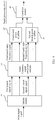
- an embodiment of this application provides an architecture of a radio frequency signal transmitter.
- the radio frequency signal transmitter specifically includes: an input interface 11, a channel encoder 12, a symbol encoder 13, a baseband filter 14, and an IQ (In-phase/Quadrature, in-phase/quadrature) modulator 15, an intermediate frequency local oscillator 16, an intermediate frequency filter 17, an upconverter 18, a radio frequency local oscillator 19, a power amplifier 20, and an antenna 21.
- a basic function of the radio frequency signal transmitter shown in FIG. 2 is as follows: A digital signal (data (data) or noise (noise)) enters from the input interface 11.
- one I/Q signal that is, one digital signal, is generated in the symbol encoder (Symbol Encoder) 13.
- the I/Q signal includes an I signal and a Q signal, where the I signal and the Q signal are orthogonal to each other.
- the I/Q signal is filtered by using the baseband filter (Baseband Filter) 14, and then is upconverted by the I/Q modulator (IQ Modulator) 15 based on a signal in the intermediate frequency local oscillator (IF LO, Intermediate Frequency local oscillator) 16 to an IF intermediate frequency, to obtain an intermediate frequency signal of a predetermined amplitude and a predetermined phase.
- Baseband Filter Baseband Filter
- I/Q modulator IQ Modulator
- the intermediate frequency signal After passing through the intermediate frequency filter 17 (IF Filter), the intermediate frequency signal is upconverted by the upconverter (upconverter) 18 based on a signal in the radio frequency local oscillator (RF LO, Radio Frequency local oscillator) 19, to obtain a radio frequency RF signal, that is, a radio frequency signal, of a predetermined amplitude and a predetermined phase. Therefore, a plurality of groups of radio frequency signals of predetermined amplitudes and predetermined phases may be generated.
- One radio frequency signal corresponds to one I/Q signal generated by the symbol encoder 13, and an amplitude and a phase of the radio frequency signal are determined by an I signal and a Q signal in the corresponding I/Q signal.
- the radio frequency signal is fed into the power amplifier (amplifier) 20, and is amplified by the power amplifier 20 and then transmitted by using the antenna F.
- FIG. 2 is merely a block diagram of a relatively common transmitter in which two times of frequency conversion, intermediate frequency conversion and radio frequency conversion, are performed.
- transmitters in which a plurality of times of frequency conversion are performed or a baseband signal is directly converted into a radio frequency signal are also applicable to this application.
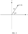
- determining or adjustment of the amplitude and the phase of the radio frequency signal may be implemented in the I/Q modulator 15. Referring to FIG. 3 , a principle thereof is as follows: An I signal and a Q signal are two orthogonal signals, and may be considered as points in a rectangular coordinate system (x, y).
- an amplitude value of the I signal is equivalent to a point on an x-axis
- an amplitude value of the Q signal is equivalent to a point on a y-axis. Therefore, changing amplitudes and phases of the I signal and the Q signal is equivalent to changing locations of points that are in the coordinate system (x, y) and that correspond to the I signal and the Q signal.
- a signal I+j ⁇ Q passing through the I/Q modulator 15 may represent any point (vector) in the coordinate system.
- the amplitude and the phase of the radio frequency signal to be generated may alternatively be implemented in a process in which the channel encoder 12 and the symbol encoder 13 perform digital signal processing.
- an embodiment of this application provides a signal processing circuit, and the signal processing circuit may be applied to a radio frequency signal transmitter.
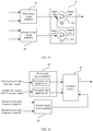
- the signal processing circuit includes a splitter module 41, a radio frequency signal conversion module 42, a first branch power amplifier 43, a second branch power amplifier 44, and a combiner module 45.
- the splitter module 41 is connected to the radio frequency signal conversion module 42
- the radio frequency signal conversion module 42 is connected to the first branch power amplifier 43 and the second branch power amplifier 44
- the first branch power amplifier 43 and the second branch power amplifier 44 are connected to the combiner module 45.
- the splitter module 41 is configured to: receive a first digital signal, split the first digital signal into at least one first branch digital signal and at least one second branch digital signal based on an input power of the first digital signal, and output the at least one first branch digital signal and the at least one second branch digital signal to the radio frequency signal conversion module 42, where a ratio of an amplitude of the at least one first branch digital signal to an amplitude of the at least one second branch digital signal varies with the input power of the first digital signal, and/or a phase difference between the at least one first branch digital signal and the at least one second branch digital signal varies with the input power of the first digital signal.
- the radio frequency signal conversion module 32 is configured to: convert the at least one first branch digital signal and the at least one second branch digital signal into at least one first branch radio frequency signal and at least one second branch radio frequency signal 32, and output the at least one first branch radio frequency signal and the at least one second branch radio frequency signal.
- the first branch power amplifier is configured to: amplify the received at least one first branch radio frequency signal, and output the amplified at least one first branch radio frequency signal to the combiner module.
- the second branch power amplifier is configured to: amplify the received at least one second branch radio frequency signal, and output the amplified at least one second branch radio frequency signal to the combiner module.
- the first branch power amplifier 43 is configured to: amplify received at least one first radio frequency signal, and output the amplified at least one first radio frequency signal to the combiner module 45.
- the second branch power amplifier 44 is configured to: amplify received at least one second radio frequency signal, and output the amplified at least one second radio frequency signal to the combiner module 45.
- the combiner module 45 is configured to: receive at least one output signal output by the first branch power amplifier 43 and at least one output signal output by the second branch power amplifier 44; and adjust, based on the at least one output signal output by the second branch power amplifier 44, the at least one output signal output by the first branch power amplifier 43, and output the adjusted at least one output signal.
- the first branch power amplifier 43 may output the at least one output signal, and the at least one output signal may be directly input to the combiner module 45.
- the plurality of output signals may be combined and then sent to the combiner module 45.
- the first branch power amplifier 43 may output only one output signal or output one signal that is obtained after a plurality of output signals are combined.
- the second branch power amplifier 44 may output the at least one output signal, and the at least one output signal may be directly input into the combiner module 45.
- the plurality of output signals may be combined and then sent to the combiner module 45.
- one signal (certainly, the second branch power amplifier 44 may output only one output signal or output one signal that is obtained after a plurality of output signals are combined) is output to the combiner module is used for description.
- the radio frequency signal conversion module 32 may include one digital-to-analog converter (Analog-to-Digital Converter, ADC) or a plurality of digital-to-analog converters. It may be understood that when the radio frequency signal conversion module 32 includes one digital-to-analog converter, the digital-to-analog converter may convert the at least one first branch digital signal and the at least one second branch digital signal into the at least one first branch radio frequency signal and the at least one second branch radio frequency signal, and output the at least one first branch radio frequency signal and the at least one second branch radio frequency signal. When the radio frequency signal conversion module 32 includes a plurality of digital-to-analog converters, each digital-to-analog converter converts one branch digital signal to a radio frequency signal.
- ADC Analog-to-Digital Converter
- an ADC 1 converts one first branch digital signal into one first branch radio frequency signal
- an ADC 2 converts one second branch digital signal into one second branch radio frequency signal.
- the splitter module 41 may be an independent function entity or device connected to the symbol encoder 13, or the splitter module 41 may be integrated into the symbol encoder 13, or serve as one function module of the symbol encoder 13. In this case, the symbol encoder 13 has a function of the splitter module 41.
- the radio frequency signal conversion module 32 may include at least one radio frequency signal processing channel that includes the baseband filter 14, the I/Q (In-phase/Quadrature, in-phase/quadrature) modulator 15, the intermediate frequency local oscillator 16, the intermediate frequency filter 17, the frequency booster 18, and the radio frequency local oscillator 19.
- Each radio frequency signal processing channel can implement a function of converting at least one digital signal into at least one radio frequency signal.
- the radio frequency signal processing channel may alternatively include one or more other devices, or one or more devices in the radio frequency signal processing channel are omitted. This is not limited in this application, and is subject to the foregoing function of the radio frequency signal conversion module 32 that can be implemented.
- the first branch power amplifier 43, the second branch power amplifier 44, and the combiner module 45 jointly constitute the foregoing power amplifier 20.
- the splitter module can split the first digital signal into the at least one first branch digital signal and the at least one second branch digital signal based on the input power of the first digital signal
- the radio frequency signal conversion module can convert the at least one first branch digital signal and the at least one second branch digital signal into the at least one first branch radio frequency signal and the at least one second branch radio frequency signal, and output the at least one first branch radio frequency signal and the at least one second branch radio frequency signal, where the ratio of the amplitude of the at least one first branch digital signal to the amplitude of the at least one second branch digital signal varies with the input power of the first digital signal, and/or the phase difference between the at least one first branch digital signal and the at least one second branch digital signal varies with the input power of the first digital signal, the at least one first branch radio frequency signal entering the first branch power amplifier and the at least one second branch radio frequency signal entering the second branch power amplifier are adjusted independently from each other.
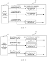
- the first branch power amplifier 43 includes a first signal splitter 431 and at least two first power sub-amplifiers connected to the first signal splitter 431.
- two first power sub-amplifiers (432 and 433) are used as an example.
- the first signal splitter 431 has an input port connected to the radio frequency signal conversion module 42, and receives one first branch radio frequency signal, and at least two output ports of the first signal splitter 431 each are connected to one first power sub-amplifier (432 or 433).
- the first signal splitter 431 is configured to: split the first branch radio frequency signal into at least two radio frequency signals, and output the at least two radio frequency signals.
- the first branch power amplifier 43 may alternatively include a plurality of first signal splitters. For a manner of connecting to each first signal splitter, refer to the connection manner shown in FIG. 5 .
- the second branch power amplifier 44 includes a second signal splitter 441 and at least two second power sub-amplifiers connected to the second signal splitter 441.
- two first power sub-amplifiers (442 and 443) are used as an example.
- the second signal splitter 441 has an input port connected to the radio frequency signal conversion module, and receives one second branch radio frequency signal, and at least two output ports of the second signal splitter 441 each are connected to one second power sub-amplifier (442 or 443).
- the second signal splitter 441 is configured to: split the second branch radio frequency signal into at least two radio frequency signals, and output the at least two radio frequency signals.
- the second branch power amplifier 44 may alternatively include a plurality of second signal splitters. For a manner of connecting to each second signal splitter, refer to the connection manner shown in FIG. 6 .
- the first branch power amplifier 43 includes at least one first power sub-amplifier. Any first power sub-amplifier in the at least one first power sub-amplifier has an input port connected to the radio frequency signal conversion module 42, and receives one first branch radio frequency signal.
- a first branch radio frequency signal m1 is input into a first power sub-amplifier G1; and a first branch radio frequency signal m2 is output into a second power sub-amplifier G2, ..., and a first branch radio frequency signal mk is input into a second power sub-amplifier Gk.
- the second branch power amplifier 44 includes at least one second power sub-amplifier. Any second power sub-amplifier in the at least one second power sub-amplifier has an input port connected to the radio frequency signal conversion module, and receives one second branch radio frequency signal.
- a second branch radio frequency signal n1 is input into a second power sub-amplifier HI
- a second branch radio frequency signal n2 is input into a second power sub-amplifier H2, ...
- a second branch radio frequency signal nk is input into a second power sub-amplifier Hk.
- a power amplifier circuit may have a structure obtained by using any one of a combination of structures in the foregoing Example 1 to Example 4.
- a form of a signal output by the first branch power amplifier 43 to the combiner module 45 is not limited.
- the first branch power amplifier 43 may output at least one output signal, and the at least one output signal may be directly input to the combiner module 45.
- the signals may be combined and then sent to the combiner module 45.
- a form of a signal output by the second branch power amplifier 44 to the combiner module 45 is not limited.
- the second branch power amplifier 44 may output at least one output signal, and the at least one output signal may be directly input to the combiner module 45.
- the signals may be combined and then sent to the combiner module 45.
- the first branch power amplifier 21 may include at least one of the following power amplifier types: a single-tube power amplifier, a Doherty power amplifier, a Chireix power amplifier, an outphasing power amplifier, and an envelope tracking ET power amplifier.
- the second branch power amplifier 22 may include at least one of the following power amplifier types: a single-tube power amplifier, a Doherty power amplifier, a Chireix power amplifier, an outphasing power amplifier, and an ET power amplifier.
- FIG. 9 shows a manner of connecting the first branch power amplifier, the second branch power amplifier, and the combiner module.
- the combiner module 45 includes a three-port device, the first branch power amplifier 43 includes one output port, and the second branch power amplifier 44 includes one output port.
- a first port of the three-port device is connected to the output port of the first branch power amplifier 43, and the first branch power amplifier 43 is specifically configured to: amplify the received at least one first branch radio frequency signal, and output the amplified at least one first branch radio frequency signal to the first port of the three-port device.
- the first branch power amplifier 43 includes only one first power sub-amplifier, the first branch power amplifier 43 outputs an output signal in the first power sub-amplifier; or if the first branch power amplifier 43 includes two or more first power sub-amplifiers, the first branch power amplifier 43 further needs to combine output signals in the two or more first power sub-amplifiers.
- the two or more first power sub-amplifiers may form the first branch power amplifier with reference to the structure in Example 1 shown in FIG. 5 or the structure in Example 3 shown in FIG. 7 .
- a third port of the three-port device is connected to the output port of the second branch power amplifier 44, and the second branch power amplifier 44 is specifically configured to: amplify the received at least one second branch radio frequency signal, and output the amplified at least one second branch radio frequency signal to the third port of the three-port device. It should be noted that, if the second branch power amplifier 44 includes only one second power sub-amplifier, the second branch power amplifier 44 outputs an output signal in the second power sub-amplifier; or if the second branch power amplifier 44 includes two or more second power sub-amplifiers, the second branch power amplifier 44 further needs to combine output signals in the two or more second power sub-amplifiers.
- the two or more second power sub-amplifiers may form the first branch power amplifier with reference to the structure in Example 2 shown in FIG. 6 or the structure in Example 4 shown in FIG. 8 .
- the three-port device is configured to: adjust, based on the signal received through the third port, the signal received through the first port, and output the signal through a second port of the three-port device.
- Atypical three-port device is a circulator. As shown in FIG. 9 , a three-port device is implemented by using a circulator. The circulator implements (approximate) unidirectional transmission from a port 3 to a port 1, and (approximate) unidirectional transmission from the port 1 to a port 2.
- an effect of an output impedance of a circuit connected to the port 1 is adjusted by changing an input (current) at the port 3.
- the port 1 of the circulator is also referred to as an input port
- the port 2 is also referred to as an output port
- the port 3 is also referred to as an isolated port.
- I 1 I 2 ⁇ I 3
- I 2 I 1 + I 3
- V 3 I 3 ⁇ Z 0
- V 1 is a voltage at the port 1
- I 1 is a current at the port 1
- V 2 is a voltage at the port 2
- I 2 is a current at the port 2
- I 3 is a voltage at the port 3
- V 3 is a current at the port 3
- Z 0 is a characteristic impedance of the circulator.
- Load pull on the first branch power amplifier 43 can be implemented by changing a phase and an amplitude of an output current I 3 of the second branch power amplifier 44. In this way, the power amplifier can work efficiently in high power back-off.
- a first branch power amplifier 43 may include a two-branch Doherty power amplifier, and input a first branch radio frequency signal.
- a second branch power amplifier 44 is a single-tube class-B power amplifier, and inputs a second branch radio frequency signal.
- the Doherty power amplifier includes a power divider g (divider, where the power divider may use a hybrid coupler), a main power amplifier (main PA), and a peaking power amplifier (peak PA, or an auxiliary PA, auxiliary power amplifier).
- the power divider g, the main power amplifier (main PA), and the peaking power amplifier (peak PA) are connected to a port 1 of a circulator 45 by using an impedance matching network.
- the power divider g splits a first branch radio frequency signal into two signals, and respectively transmits the two signals to the main power amplifier (main PA) and the peaking power amplifier (peak PA).
- the impedance matching network includes an input impedance matching circuit c1 disposed between the power divider g and the main power amplifier (main PA), and an input impedance matching circuit c2 disposed between the power divider g and the peaking power amplifier (peak PA), a first output impedance conversion circuit c3 disposed at an output port of the main power amplifier (main PA), a second output impedance conversion circuit c4 disposed at an output port of the peaking power amplifier (peak PA), and an output impedance matching circuit c5 connecting the first output impedance conversion circuit c3 and the second output impedance conversion circuit c4 to of the port 1 of the circulator 23.
- the second branch power amplifier 44 is a single-tube class-B power amplifier, and a larger amplitude of a fundamental voltage of the second branch power amplifier 44 indicates a higher output power and higher circuit efficiency of the power amplifier.
- an efficiency curve of the Doherty power amplifier is similar to that of the single-tube class-B power amplifier.
- the peaking power amplifier peak PA
- a power amplifier circuit maintains relatively high efficiency in a back-off range.
- an output current of the Doherty power amplifier of the first branch power amplifier 43 and an output current of the single-tube class-B power amplifier of the second branch power amplifier 22 are in same phase or in reverse phase.
- the first branch power amplifier 43 and the second branch power amplifier 44 each can be at a high-efficiency point or in a zero-output power state by controlling an output current of the second branch power amplifier 22, to implement high-efficiency output of the power amplifier circuit.
- any radio frequency signal in the at least one first branch radio frequency signal input into the first branch power amplifier 43 is different from any radio frequency signal in the at least one second branch radio frequency signal input into the second branch power amplifier 44. Therefore, provided that at least one first branch radio frequency signal input into the first branch power amplifier and at least one second branch radio frequency signal input into the second branch power amplifier are independently adjusted, a phase and an amplitude of each radio frequency signal in radio frequency signals received by the two branch power amplifiers can satisfy that the two branch power amplifiers are respectively at a high-efficiency point or in a zero output power state, so that the output efficiency of the power amplifier circuit is maximized. In other words, in the solution of this application, signals of the two branch power amplifiers are more flexibly adjusted. Therefore, power amplification efficiency of the signal processing circuit is improved.
- a ratio of saturation output powers of the Main PA and the peaking PA of the Doherty power amplifier of the first branch power amplifier and the single-tube class-B power amplifier of the second branch power amplifier is 12:12:1 (the power ratio may be any ratio, and is not limited to this example).
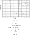
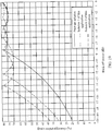
- FIG. 11 to FIG. 15 show simulation of characteristic data of each part of a power amplifying circuit of the signal processing circuit.
- FIG. 11 shows a relationship between a linear back-off voltage Vout and a drain current Idrain of each of the main PA, the peak PA, and the single-tube class-B power amplifier of the two branch power amplifiers.
- FIG. 12 shows a relationship between a drain voltage Vdrain and the linear back-off voltage Vout.
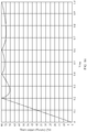
- FIG. 13 shows an efficiency curve in power back-off, where a horizontal axis represents a back-off power in a unit of dB (Back-off Power), and a vertical axis represents drain output efficiency (Drain Output Efficiency).
- FIG. 14 shows an efficiency curve in linear back-off, where a horizontal axis represents a back-off voltage Vout, and a vertical axis represents drain output efficiency (Drain Efficiency).
- FIG. 15 shows a relationship between linear back-off and a linear load-pull ratio of each of the main PA, the peak PA, and the single-tube class-B power amplifier of the two branch power amplifiers. It can be learned from FIG. 11 to FIG. 15 that, four or more high efficiency points can be obtained in high power back-off by adjusting signal amplitudes and phases of the first branch radio frequency signal and the second branch radio frequency signal in the two branch power amplifiers.
- the Doherty power amplifier shown in FIG. 10 may be replaced with an ADoherty (Asymmetric Doherty, asymmetric Doherty) power amplifier or a Chireix power amplifier.
- ADoherty Asymmetric Doherty, asymmetric Doherty
- Chireix a Chireix power amplifier
- the second branch power amplifier in this embodiment of this application may alternatively be replaced with another type of a single-tube power amplifier, a Doherty power amplifier, a Chireix power amplifier, an outphasing power amplifier, or an ET power amplifier, or the second branch power amplifier may include at least one of the foregoing power amplifiers.
- FIG. 16 is a schematic structural diagram of a three-branch Doherty power amplifier or a three-branch Chireix power amplifier.
- a structure of the three-branch Doherty power amplifier or the three-branch Chireix power amplifier is similar to that of the two-branch Doherty power amplifier of the first branch power amplifier shown in FIG. 10 , and the three-branch Doherty power amplifier or the three-branch Chireix power amplifier includes one main power amplifier (main PA), two peaking power amplifiers (a peak PA 1 and a peak PA 2), and an impedance matching network.
- FIG. 17 is a schematic structural diagram of a four-branch Doherty power amplifier or a four-branch Chireix power amplifier.
- the four-branch Doherty power amplifier or the four-branch Chireix power amplifier includes a main power amplifier (main PA), three peaking power amplifiers (a peak PA 1, a peak PA2, and a peak PA3), and an impedance matching network.
- FIG. 18 is a schematic structural diagram of an outphasing power amplifier.
- the outphasing power includes a signal splitter (signal component separator), two power amplifiers (a PA 1 and a PA 2), and an outphasing combiner.
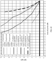
- FIG. 19 shows a curve of back-off power and drain output efficiency of a three-branch Doherty power amplifier in a prior-art solution and a curve of back-off power and drain output efficiency of a power amplifier according to an embodiment of this application.
- solution 1 of this application an example in which a first branch power amplifier uses a class-AB power amplifier and a second branch power amplifier uses a single-tube class-B power amplifier is used in this embodiment of this application.
- solution 2 of this application an example in which a first branch power amplifier uses a two-branch Doherty power amplifier, and a second branch power amplifier uses a single-tube class-B power amplifier is used in this embodiment of this application.
- Load pull on the first branch power amplifier by the second branch power amplifier is implemented by controlling phases and amplitudes of radio frequency signals input by the two branch power amplifiers, thereby implementing high-efficiency work in higher-power back-off.
- a ratio a of a total peak power of the first branch power amplifier to a total peak power of the second branch power amplifier is related to a back-off range in which the entire power amplifier circuit works.
- a larger ratio indicates a larger back-off range of the power amplifier circuit, and a theoretical maximum back-off value is 10*1g(a+1).
- the ratio affects a quantity of high-efficiency points (extreme points) that can be obtained within the back-off range. When the ratio is greater than 3 and less than 8, three high-efficiency extreme points can be obtained. When the ratio is greater than 8, four high-efficiency extreme points can be obtained.
- curve 1 of a prior-art solution provides a curve of a back-off power of a three-branch Doherty power amplifier and a load-pull ratio (LPR, Load pull ratio) of a main PA in the prior art
- curve 2 of a prior-art solution provides a curve of a back-off power of a three-branch Doherty power amplifier and an LPR of a peak PA 1 in the prior art
- curve 3 of a prior-art solution provides a curve of a back-off power of a three-branch Doherty power amplifier and an LPR of a peak PA 2 in the prior art
- curve 1 of solution 1 of this application provides a curve of a back-off power of a class-AB power amplifier used by a first branch power amplifier and an LPR of a second branch power amplifier in this embodiment of this application
- curve 2 of solution 1 of this application provides a curve of a back-off power of a back-off power of a back-off power of a
- a three-port device 45 includes a first isolator 451 and a second isolator 452.
- An input port of the first isolator 451 is connected to a first port (port 1) of the three-port device, and an output port of the first isolator is connected to a second port (port 2) of the three-port device.
- An input port of the second isolator 452 is connected to a third port (port 3) of the three-port device, and an output port of the second isolator is connected to the first port (port 1) of the three-port device. Because of a unidirectional conduction function of an isolator, a function similar to that of a circulator is implemented.
- the second isolator 452 is configured to transmit a signal received through the third port of the three-port device to the input port of the first isolator.
- the first isolator 451 is configured to adjust, based on the signal received through the third port of the three-port device, a signal received through the first port of the three-port device, and output the signal through the second port of the three-port device.
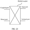
- a combiner module 45 may alternatively be a four-port device, and the four-port device may be a rat-race coupler or a hybrid coupler.
- a first branch power amplifier 43 includes a first output port and a second output port
- a second branch power amplifier 44 includes an output port.
- the first output port of the first branch power amplifier 43 is connected to a first port (port 1) of the four-port device; the second output port of the first branch power amplifier 43 is connected to a second port (port 2) of the four-port device; and the output port of the second branch power amplifier 44 is connected to a third port (port 3) of the four-port device.
- the first branch power amplifier 43 is specifically configured to: receive at least two first branch radio frequency signals; and amplify the received at least two first branch radio frequency signals, and output the at least two amplified first branch radio frequency signals to the first port and the second port of the four-port device.
- the first branch power amplifier 43 includes a first power sub-amplifier G1 and a first power sub-amplifier G2.
- One first branch radio frequency signal is amplified and output by the first power sub-amplifier G1
- another first branch radio frequency signal is amplified and output by the first power sub-amplifier G2.
- the second branch power amplifier 44 is specifically configured to: amplify the received at least one second branch radio frequency signal (n1-nk), and output the amplified at least one second branch radio frequency signal (n1-nk) to the third port of the four-port device.
- the four-port device is configured to: adjust, based on the signal received through the third port, the signal received through the first port and the signal received through the second port; and combine the adjusted signal received through the first port and the adjusted signal received through the second port, and output a combined signal to a fourth port (port 4) of the four-port device.
- the first branch power amplifier when the first branch power amplifier includes more power sub-amplifiers, or amplifies two or more radio frequency signals, the first branch power amplifier may further combine some or all of a plurality of amplified radio frequency signals to obtain two radio frequency signals, and respectively output the two radio frequency signals to the second port and the third port of the four-port device.
- the second branch power amplifier when the second branch power amplifier includes more than one power sub-amplifier, or amplifies more than one radio frequency signal, the second branch power amplifier may further combine the more than one amplified radio frequency signal to obtain one combined radio frequency signal, and output the combined radio frequency signal to the third port of the four-port device.
- an amplitude of a first output signal output by the first power sub-amplifier G1 is the same as an amplitude of a second output signal output by the first power sub-amplifier G2, and a phase difference is 90 degrees.
- An output port of the first power sub-amplifier G1 and an output port of the first power sub-amplifier G2 are respectively connected to a coupled port (coupled port) and a direct port (direct port) of the hybrid coupler.
- the first output signal and the second output signal are combined and then are output from an input port (input port).
- An isolated (isolated) port has no signal output.
- a combined signal output by the second branch power amplifier 44 is input from an isolated (isolated) port, and is split into two signals with a same amplitude and a phase difference of 90 degrees.
- the combined signal is output from the coupled port (coupled port) and the direct port (direct port), and the input port (input port) has no output. Therefore, (approximate) unidirectional transmission from the isolated port to the coupled port and the direct port and (approximate) unidirectional transmission from the coupled port and the direct port to the isolated port are implemented.
- the first output signal and the second output signal that are input at the coupled port (coupled port) and the direct port (direct port) are separately adjusted by using the two signals obtained by splitting the combined signal that is input at the isolated (isolated) port.
- the adjusted first output signal and the adjusted second output signal are combined and then are output by using the input port (input port) of the hybrid coupler.
- the combiner module 45 uses a four-port device, referring to FIG. 24 , if a first branch power amplifier 43 receives only one first branch radio frequency signal, the first branch power amplifier 43 includes a signal splitter 431, a first power sub-amplifier 432, and a second power sub-amplifier 433.
- a radio frequency signal conversion module 42 connected to an input port of the signal splitter 431 receives one first branch radio frequency signal.
- a first output port of the signal splitter 431 is connected to an input port of the first power sub-amplifier 432, and an output port of the first power sub-amplifier 432 is connected to a first port of the four-port device.
- a second output port of the signal splitter 433 is connected to an input port of the first power sub-amplifier 433, and an output port of the first power sub-amplifier 432 is connected to a first port of the four-port device.
- the signal splitter 431 is configured to: split the first branch radio frequency signal into at least two radio frequency signals, and separately input the at least two radio frequency signals to the first power sub-amplifier 432 and the first power sub-amplifier 433.
- An output port of the second branch power amplifier 44 is connected to a third port of the four-port device, and is specifically configured to amplify received at least one second radio frequency signal, combine the amplified signal, and output a combined signal to the third port of the four-port device.
- the four-port device is configured to: adjust, based on the signal received through the third port, the signal received through the first port and the signal received through the second port; and combine the adjusted signal received through the first port and the adjusted signal received through the second port, and output a combined signal to a fourth port of the four-port device.
- the signal splitter 431 may use a hybrid coupler.
Landscapes
- Engineering & Computer Science (AREA)
- Power Engineering (AREA)
- Computer Networks & Wireless Communication (AREA)
- Signal Processing (AREA)
- Amplifiers (AREA)
Applications Claiming Priority (1)
| Application Number | Priority Date | Filing Date | Title |
|---|---|---|---|
| PCT/CN2017/118071 WO2019119436A1 (zh) | 2017-12-22 | 2017-12-22 | 一种信号处理电路、射频信号发射机和通信设备 |
Publications (3)
| Publication Number | Publication Date |
|---|---|
| EP3720004A1 true EP3720004A1 (de) | 2020-10-07 |
| EP3720004A4 EP3720004A4 (de) | 2020-12-16 |
| EP3720004B1 EP3720004B1 (de) | 2025-08-27 |
Family
ID=66992898
Family Applications (1)
| Application Number | Title | Priority Date | Filing Date |
|---|---|---|---|
| EP17935244.8A Active EP3720004B1 (de) | 2017-12-22 | 2017-12-22 | Signalverarbeitungsschaltung, funkfrequenzsignalsender und kommunikationsvorrichtung |
Country Status (5)
| Country | Link |
|---|---|
| US (1) | US11444362B2 (de) |
| EP (1) | EP3720004B1 (de) |
| CN (1) | CN111566940B (de) |
| BR (1) | BR112020012575A2 (de) |
| WO (1) | WO2019119436A1 (de) |
Families Citing this family (16)
| Publication number | Priority date | Publication date | Assignee | Title |
|---|---|---|---|---|
| CN108599785B (zh) * | 2018-03-30 | 2019-11-19 | 维沃移动通信有限公司 | 基于毫米波通信的射频系统、发射功率的调整方法及终端 |
| EP4142150B1 (de) * | 2020-06-04 | 2024-07-10 | Mitsubishi Electric Corporation | Doherty-verstärker |
| CN112886999B (zh) * | 2021-01-25 | 2021-10-26 | 维沃移动通信有限公司 | 射频电路、电子设备及射频控制方法 |
| CN114844469B (zh) * | 2021-02-02 | 2025-09-12 | 大唐移动通信设备有限公司 | 一种功率控制系统及控制方法 |
| CN113064368B (zh) * | 2021-03-18 | 2022-03-08 | 科海技术股份有限公司 | 一种大功率射频电源系统 |
| CN115347903A (zh) * | 2021-05-13 | 2022-11-15 | 中国电信股份有限公司 | 移频分布近端机、系统和信号移频处理方法 |
| EP4364291A1 (de) * | 2021-06-30 | 2024-05-08 | Telefonaktiebolaget LM Ericsson (publ) | Verstärkerschaltung und verfahren zum betrieb einer verstärkerschaltung |
| WO2023032513A1 (ja) * | 2021-09-02 | 2023-03-09 | 株式会社村田製作所 | 高周波回路および通信装置 |
| CN116707564B (zh) * | 2022-02-25 | 2026-05-29 | 华为技术有限公司 | 射频前端电路和电子设备 |
| CN115297490A (zh) * | 2022-07-27 | 2022-11-04 | 欧智通科技股份有限公司 | 一种扩展wi-fi辐射范围的装置 |
| WO2024026629A1 (zh) * | 2022-08-01 | 2024-02-08 | 华为技术有限公司 | 一种功率放大装置、射频拉远单元、基站以及通信系统 |
| CN119999151A (zh) * | 2022-10-18 | 2025-05-13 | 华为技术有限公司 | 一种功放设备、射频拉远单元及基站 |
| CN115765781B (zh) * | 2022-11-28 | 2026-04-14 | 国网河南省电力公司南阳供电公司 | 变电站超高频rfid读写装置及读写方法 |
| WO2024245555A1 (en) * | 2023-06-01 | 2024-12-05 | Huawei Technologies Co., Ltd. | Power amplifier for reduced load pull ratio |
| CN119966370A (zh) * | 2023-11-09 | 2025-05-09 | 上海华为技术有限公司 | 一种功率放大电路、射频生成设备和通信系统 |
| CN120275754B (zh) * | 2025-05-29 | 2025-08-12 | 中国电子科技集团公司第二十九研究所 | 一种射频资源动态调配测试系统和方法 |
Family Cites Families (16)
| Publication number | Priority date | Publication date | Assignee | Title |
|---|---|---|---|---|
| US6054894A (en) * | 1998-06-19 | 2000-04-25 | Datum Telegraphic Inc. | Digital control of a linc linear power amplifier |
| JP4786021B2 (ja) | 2000-09-05 | 2011-10-05 | 三菱電機株式会社 | 高周波増幅器、フィードフォワード増幅器および歪み補償増幅器 |
| US20050134377A1 (en) * | 2003-12-23 | 2005-06-23 | Dent Paul W. | Doherty amplifier |
| CN101675584B (zh) * | 2007-03-30 | 2012-10-03 | 北电网络有限公司 | 放大器预失真系统和方法 |
| US8837629B2 (en) * | 2011-05-11 | 2014-09-16 | Fadhel M Ghannouchi | Extended bandwidth digital Doherty transmitter |
| CN101640562B (zh) * | 2009-08-17 | 2013-05-01 | 中兴通讯股份有限公司 | 多输入多输出系统和方法 |
| KR101094067B1 (ko) * | 2009-09-25 | 2011-12-15 | 전자부품연구원 | 클래스 f 및 인버스 클래스 f 도허티 증폭기 |
| US9571042B2 (en) * | 2012-07-26 | 2017-02-14 | Telefonaktiebolaget L M Ericsson (Publ) | Digital upconversion for multi-band multi-order power amplifiers |
| SE541265C2 (en) * | 2012-07-31 | 2019-05-28 | Fadhel Ghannouchi | Extended bandwidth digital doherty transmitter |
| US8824978B2 (en) * | 2012-10-30 | 2014-09-02 | Eta Devices, Inc. | RF amplifier architecture and related techniques |
| CN103518331B (zh) * | 2013-04-24 | 2015-05-27 | 华为技术有限公司 | 发射机和用于信号发射的方法 |
| CN105375883B (zh) * | 2014-08-13 | 2020-10-30 | 天工方案公司 | 具有可调阻抗终端电路的多尔蒂功率放大器组合器 |
| CN106506014B (zh) * | 2015-09-06 | 2019-09-06 | 上海中兴软件有限责任公司 | 发射机及信号输出方法 |
| US9787259B2 (en) * | 2015-11-06 | 2017-10-10 | Infineon Technologies Ag | Outphasing power amplifier signal splitter using next stage input impedance and multiple biasing |
| CN106452370A (zh) * | 2016-10-12 | 2017-02-22 | 杭州电子科技大学 | 一种基于非对称结构的高回退Doherty功率放大器及其实现方法 |
| CN106374863B (zh) * | 2016-10-12 | 2019-01-01 | 杭州电子科技大学 | 一种提高功率回退动态范围的Doherty功率放大器及其实现方法 |
-
2017
- 2017-12-22 WO PCT/CN2017/118071 patent/WO2019119436A1/zh not_active Ceased
- 2017-12-22 CN CN201780097831.7A patent/CN111566940B/zh active Active
- 2017-12-22 BR BR112020012575-0A patent/BR112020012575A2/pt active IP Right Grant
- 2017-12-22 EP EP17935244.8A patent/EP3720004B1/de active Active
-
2020
- 2020-06-22 US US16/908,321 patent/US11444362B2/en active Active
Also Published As
| Publication number | Publication date |
|---|---|
| CN111566940B (zh) | 2021-08-13 |
| EP3720004A4 (de) | 2020-12-16 |
| EP3720004B1 (de) | 2025-08-27 |
| WO2019119436A1 (zh) | 2019-06-27 |
| US20200321673A1 (en) | 2020-10-08 |
| CN111566940A (zh) | 2020-08-21 |
| US11444362B2 (en) | 2022-09-13 |
| BR112020012575A2 (pt) | 2020-11-24 |
Similar Documents
| Publication | Publication Date | Title |
|---|---|---|
| US11444362B2 (en) | Signal processing circuit, radio frequency signal transmitter, and communications device | |
| US8988147B2 (en) | Multi-way Doherty amplifier | |
| KR101936664B1 (ko) | 전력 증폭기, 무선 원격 유닛 및 기지국 | |
| US20080111622A1 (en) | Hybrid Doherty Amplifier System and Method | |
| TW200807979A (en) | Multilevel LINC transmitter | |
| SE521673C2 (sv) | Sammansatt förstärkare | |
| WO2015055242A1 (en) | Amplifier apparatus and method | |
| EP3729640A1 (de) | Leistungsverstärker und radiofrequenzvorrichtung damit | |
| KR102075813B1 (ko) | 증폭기 어셈블리 | |
| WO2013118367A1 (ja) | 送信機および送信方法 | |
| CN111049480B (zh) | 一种提高Doherty功放线性效率的方法及装置 | |
| CN101110595A (zh) | 多级linc发射器 | |
| US20170244366A1 (en) | Driver circuit for composite power amplifier | |
| WO2008099724A1 (en) | Linc transmission circuit and communication device using the same | |
| JP2014175760A (ja) | 非対称ドハティ電力増幅器 | |
| EP2602931B1 (de) | Verstärker | |
| CN101286962B (zh) | 一种载波抵消射频预失真功放实现装置和方法 | |
| CN106102156A (zh) | 基于多天线的线性化传输方法 | |
| WO2021005633A1 (ja) | アウトフェージング増幅器及び通信装置 | |
| CN117375534A (zh) | 功率放大器和功率放大方法 | |
| EP4583470A1 (de) | Leistungsverstärkervorrichtung, fernfunkeinheit und basisstation | |
| CN110199483B (zh) | 一种信号处理方法及设备 | |
| EP3553946B1 (de) | Hochfrequenzschaltung, sender, basisstation und benutzerendgerät | |
| CN118160220A (zh) | 功率放大装置和无线通信装置 | |
| US9515614B2 (en) | Amplifier device and wireless communication device |
Legal Events
| Date | Code | Title | Description |
|---|---|---|---|
| STAA | Information on the status of an ep patent application or granted ep patent |
Free format text: STATUS: THE INTERNATIONAL PUBLICATION HAS BEEN MADE |
|
| PUAI | Public reference made under article 153(3) epc to a published international application that has entered the european phase |
Free format text: ORIGINAL CODE: 0009012 |
|
| STAA | Information on the status of an ep patent application or granted ep patent |
Free format text: STATUS: REQUEST FOR EXAMINATION WAS MADE |
|
| 17P | Request for examination filed |
Effective date: 20200701 |
|
| AK | Designated contracting states |
Kind code of ref document: A1 Designated state(s): AL AT BE BG CH CY CZ DE DK EE ES FI FR GB GR HR HU IE IS IT LI LT LU LV MC MK MT NL NO PL PT RO RS SE SI SK SM TR |
|
| AX | Request for extension of the european patent |
Extension state: BA ME |
|
| A4 | Supplementary search report drawn up and despatched |
Effective date: 20201117 |
|
| RIC1 | Information provided on ipc code assigned before grant |
Ipc: H04B 1/04 20060101AFI20201111BHEP Ipc: H04L 25/03 20060101ALI20201111BHEP |
|
| DAV | Request for validation of the european patent (deleted) | ||
| DAX | Request for extension of the european patent (deleted) | ||
| STAA | Information on the status of an ep patent application or granted ep patent |
Free format text: STATUS: EXAMINATION IS IN PROGRESS |
|
| 17Q | First examination report despatched |
Effective date: 20230116 |
|
| GRAP | Despatch of communication of intention to grant a patent |
Free format text: ORIGINAL CODE: EPIDOSNIGR1 |
|
| STAA | Information on the status of an ep patent application or granted ep patent |
Free format text: STATUS: GRANT OF PATENT IS INTENDED |
|
| INTG | Intention to grant announced |
Effective date: 20250417 |
|
| GRAS | Grant fee paid |
Free format text: ORIGINAL CODE: EPIDOSNIGR3 |
|
| GRAA | (expected) grant |
Free format text: ORIGINAL CODE: 0009210 |
|
| STAA | Information on the status of an ep patent application or granted ep patent |
Free format text: STATUS: THE PATENT HAS BEEN GRANTED |
|
| AK | Designated contracting states |
Kind code of ref document: B1 Designated state(s): AL AT BE BG CH CY CZ DE DK EE ES FI FR GB GR HR HU IE IS IT LI LT LU LV MC MK MT NL NO PL PT RO RS SE SI SK SM TR |
|
| REG | Reference to a national code |
Ref country code: GB Ref legal event code: FG4D |
|
| REG | Reference to a national code |
Ref country code: CH Ref legal event code: EP |
|
| REG | Reference to a national code |
Ref country code: DE Ref legal event code: R096 Ref document number: 602017091518 Country of ref document: DE |
|
| REG | Reference to a national code |
Ref country code: IE Ref legal event code: FG4D |
|
| REG | Reference to a national code |
Ref country code: NL Ref legal event code: MP Effective date: 20250827 |
|
| PG25 | Lapsed in a contracting state [announced via postgrant information from national office to epo] |
Ref country code: IS Free format text: LAPSE BECAUSE OF FAILURE TO SUBMIT A TRANSLATION OF THE DESCRIPTION OR TO PAY THE FEE WITHIN THE PRESCRIBED TIME-LIMIT Effective date: 20251227 |
|
| PGFP | Annual fee paid to national office [announced via postgrant information from national office to epo] |
Ref country code: DE Payment date: 20251104 Year of fee payment: 9 |
|
| PGFP | Annual fee paid to national office [announced via postgrant information from national office to epo] |
Ref country code: GB Payment date: 20251030 Year of fee payment: 9 |
|
| PG25 | Lapsed in a contracting state [announced via postgrant information from national office to epo] |
Ref country code: NO Free format text: LAPSE BECAUSE OF FAILURE TO SUBMIT A TRANSLATION OF THE DESCRIPTION OR TO PAY THE FEE WITHIN THE PRESCRIBED TIME-LIMIT Effective date: 20251127 |
|
| REG | Reference to a national code |
Ref country code: LT Ref legal event code: MG9D |
|
| PG25 | Lapsed in a contracting state [announced via postgrant information from national office to epo] |
Ref country code: PT Free format text: LAPSE BECAUSE OF FAILURE TO SUBMIT A TRANSLATION OF THE DESCRIPTION OR TO PAY THE FEE WITHIN THE PRESCRIBED TIME-LIMIT Effective date: 20251229 |
|
| PG25 | Lapsed in a contracting state [announced via postgrant information from national office to epo] |
Ref country code: FI Free format text: LAPSE BECAUSE OF FAILURE TO SUBMIT A TRANSLATION OF THE DESCRIPTION OR TO PAY THE FEE WITHIN THE PRESCRIBED TIME-LIMIT Effective date: 20250827 |
|
| PG25 | Lapsed in a contracting state [announced via postgrant information from national office to epo] |
Ref country code: HR Free format text: LAPSE BECAUSE OF FAILURE TO SUBMIT A TRANSLATION OF THE DESCRIPTION OR TO PAY THE FEE WITHIN THE PRESCRIBED TIME-LIMIT Effective date: 20250827 Ref country code: NL Free format text: LAPSE BECAUSE OF FAILURE TO SUBMIT A TRANSLATION OF THE DESCRIPTION OR TO PAY THE FEE WITHIN THE PRESCRIBED TIME-LIMIT Effective date: 20250827 |
|
| PG25 | Lapsed in a contracting state [announced via postgrant information from national office to epo] |
Ref country code: GR Free format text: LAPSE BECAUSE OF FAILURE TO SUBMIT A TRANSLATION OF THE DESCRIPTION OR TO PAY THE FEE WITHIN THE PRESCRIBED TIME-LIMIT Effective date: 20251128 |
|
| PG25 | Lapsed in a contracting state [announced via postgrant information from national office to epo] |
Ref country code: SE Free format text: LAPSE BECAUSE OF FAILURE TO SUBMIT A TRANSLATION OF THE DESCRIPTION OR TO PAY THE FEE WITHIN THE PRESCRIBED TIME-LIMIT Effective date: 20250827 |
|
| PG25 | Lapsed in a contracting state [announced via postgrant information from national office to epo] |
Ref country code: LV Free format text: LAPSE BECAUSE OF FAILURE TO SUBMIT A TRANSLATION OF THE DESCRIPTION OR TO PAY THE FEE WITHIN THE PRESCRIBED TIME-LIMIT Effective date: 20250827 |
|
| PG25 | Lapsed in a contracting state [announced via postgrant information from national office to epo] |
Ref country code: PL Free format text: LAPSE BECAUSE OF FAILURE TO SUBMIT A TRANSLATION OF THE DESCRIPTION OR TO PAY THE FEE WITHIN THE PRESCRIBED TIME-LIMIT Effective date: 20250827 Ref country code: BG Free format text: LAPSE BECAUSE OF FAILURE TO SUBMIT A TRANSLATION OF THE DESCRIPTION OR TO PAY THE FEE WITHIN THE PRESCRIBED TIME-LIMIT Effective date: 20250827 |
|
| PG25 | Lapsed in a contracting state [announced via postgrant information from national office to epo] |
Ref country code: RS Free format text: LAPSE BECAUSE OF FAILURE TO SUBMIT A TRANSLATION OF THE DESCRIPTION OR TO PAY THE FEE WITHIN THE PRESCRIBED TIME-LIMIT Effective date: 20251127 |
|
| PG25 | Lapsed in a contracting state [announced via postgrant information from national office to epo] |
Ref country code: ES Free format text: LAPSE BECAUSE OF FAILURE TO SUBMIT A TRANSLATION OF THE DESCRIPTION OR TO PAY THE FEE WITHIN THE PRESCRIBED TIME-LIMIT Effective date: 20250827 |
|
| REG | Reference to a national code |
Ref country code: AT Ref legal event code: MK05 Ref document number: 1831245 Country of ref document: AT Kind code of ref document: T Effective date: 20250827 |
|
| PG25 | Lapsed in a contracting state [announced via postgrant information from national office to epo] |
Ref country code: RO Free format text: LAPSE BECAUSE OF FAILURE TO SUBMIT A TRANSLATION OF THE DESCRIPTION OR TO PAY THE FEE WITHIN THE PRESCRIBED TIME-LIMIT Effective date: 20250827 |
|
| PG25 | Lapsed in a contracting state [announced via postgrant information from national office to epo] |
Ref country code: SM Free format text: LAPSE BECAUSE OF FAILURE TO SUBMIT A TRANSLATION OF THE DESCRIPTION OR TO PAY THE FEE WITHIN THE PRESCRIBED TIME-LIMIT Effective date: 20250827 |
|
| PG25 | Lapsed in a contracting state [announced via postgrant information from national office to epo] |
Ref country code: DK Free format text: LAPSE BECAUSE OF FAILURE TO SUBMIT A TRANSLATION OF THE DESCRIPTION OR TO PAY THE FEE WITHIN THE PRESCRIBED TIME-LIMIT Effective date: 20250827 |
|
| PG25 | Lapsed in a contracting state [announced via postgrant information from national office to epo] |
Ref country code: AT Free format text: LAPSE BECAUSE OF FAILURE TO SUBMIT A TRANSLATION OF THE DESCRIPTION OR TO PAY THE FEE WITHIN THE PRESCRIBED TIME-LIMIT Effective date: 20250827 |
|
| PG25 | Lapsed in a contracting state [announced via postgrant information from national office to epo] |
Ref country code: IT Free format text: LAPSE BECAUSE OF FAILURE TO SUBMIT A TRANSLATION OF THE DESCRIPTION OR TO PAY THE FEE WITHIN THE PRESCRIBED TIME-LIMIT Effective date: 20250827 |
|
| PG25 | Lapsed in a contracting state [announced via postgrant information from national office to epo] |
Ref country code: CZ Free format text: LAPSE BECAUSE OF FAILURE TO SUBMIT A TRANSLATION OF THE DESCRIPTION OR TO PAY THE FEE WITHIN THE PRESCRIBED TIME-LIMIT Effective date: 20250827 |
|
| PG25 | Lapsed in a contracting state [announced via postgrant information from national office to epo] |
Ref country code: SK Free format text: LAPSE BECAUSE OF FAILURE TO SUBMIT A TRANSLATION OF THE DESCRIPTION OR TO PAY THE FEE WITHIN THE PRESCRIBED TIME-LIMIT Effective date: 20250827 Ref country code: EE Free format text: LAPSE BECAUSE OF FAILURE TO SUBMIT A TRANSLATION OF THE DESCRIPTION OR TO PAY THE FEE WITHIN THE PRESCRIBED TIME-LIMIT Effective date: 20250827 |
|
| REG | Reference to a national code |
Ref country code: DE Ref legal event code: R097 Ref document number: 602017091518 Country of ref document: DE |
|
| PG25 | Lapsed in a contracting state [announced via postgrant information from national office to epo] |
Ref country code: LT Free format text: LAPSE BECAUSE OF FAILURE TO SUBMIT A TRANSLATION OF THE DESCRIPTION OR TO PAY THE FEE WITHIN THE PRESCRIBED TIME-LIMIT Effective date: 20250827 |
|
| PLBE | No opposition filed within time limit |
Free format text: ORIGINAL CODE: 0009261 |
|
| STAA | Information on the status of an ep patent application or granted ep patent |
Free format text: STATUS: NO OPPOSITION FILED WITHIN TIME LIMIT |
|
| PG25 | Lapsed in a contracting state [announced via postgrant information from national office to epo] |
Ref country code: MC Free format text: LAPSE BECAUSE OF FAILURE TO SUBMIT A TRANSLATION OF THE DESCRIPTION OR TO PAY THE FEE WITHIN THE PRESCRIBED TIME-LIMIT Effective date: 20250827 |
|
| REG | Reference to a national code |
Ref country code: CH Ref legal event code: L10 Free format text: ST27 STATUS EVENT CODE: U-0-0-L10-L00 (AS PROVIDED BY THE NATIONAL OFFICE) Effective date: 20260708 |
|
| REG | Reference to a national code |
Ref country code: CH Ref legal event code: H13 Free format text: ST27 STATUS EVENT CODE: U-0-0-H10-H13 (AS PROVIDED BY THE NATIONAL OFFICE) Effective date: 20260723 |
|
| 26N | No opposition filed |
Effective date: 20260528 |