EP3720103B1 - Anzeige mit öffnung zur montage eines sensors - Google Patents
Anzeige mit öffnung zur montage eines sensors Download PDFInfo
- Publication number
- EP3720103B1 EP3720103B1 EP19743306.3A EP19743306A EP3720103B1 EP 3720103 B1 EP3720103 B1 EP 3720103B1 EP 19743306 A EP19743306 A EP 19743306A EP 3720103 B1 EP3720103 B1 EP 3720103B1
- Authority
- EP
- European Patent Office
- Prior art keywords
- layer
- display
- sensor
- thin film
- light emitting
- Prior art date
- Legal status (The legal status is an assumption and is not a legal conclusion. Google has not performed a legal analysis and makes no representation as to the accuracy of the status listed.)
- Active
Links
Images

Classifications
-
- H—ELECTRICITY
- H04—ELECTRIC COMMUNICATION TECHNIQUE
- H04M—TELEPHONIC COMMUNICATION
- H04M1/00—Substation equipment, e.g. for use by subscribers
- H04M1/02—Constructional features of telephone sets
- H04M1/0202—Portable telephone sets, e.g. cordless phones, mobile phones or bar type handsets
- H04M1/026—Details of the structure or mounting of specific components
- H04M1/0266—Details of the structure or mounting of specific components for a display module assembly
-
- H—ELECTRICITY
- H04—ELECTRIC COMMUNICATION TECHNIQUE
- H04M—TELEPHONIC COMMUNICATION
- H04M1/00—Substation equipment, e.g. for use by subscribers
- H04M1/02—Constructional features of telephone sets
- H04M1/0202—Portable telephone sets, e.g. cordless phones, mobile phones or bar type handsets
- H04M1/026—Details of the structure or mounting of specific components
-
- H—ELECTRICITY
- H10—SEMICONDUCTOR DEVICES; ELECTRIC SOLID-STATE DEVICES NOT OTHERWISE PROVIDED FOR
- H10K—ORGANIC ELECTRIC SOLID-STATE DEVICES
- H10K50/00—Organic light-emitting devices
- H10K50/80—Constructional details
- H10K50/84—Passivation; Containers; Encapsulations
- H10K50/841—Self-supporting sealing arrangements
-
- H—ELECTRICITY
- H10—SEMICONDUCTOR DEVICES; ELECTRIC SOLID-STATE DEVICES NOT OTHERWISE PROVIDED FOR
- H10K—ORGANIC ELECTRIC SOLID-STATE DEVICES
- H10K50/00—Organic light-emitting devices
- H10K50/80—Constructional details
- H10K50/84—Passivation; Containers; Encapsulations
- H10K50/844—Encapsulations
-
- H—ELECTRICITY
- H10—SEMICONDUCTOR DEVICES; ELECTRIC SOLID-STATE DEVICES NOT OTHERWISE PROVIDED FOR
- H10K—ORGANIC ELECTRIC SOLID-STATE DEVICES
- H10K59/00—Integrated devices, or assemblies of multiple devices, comprising at least one organic light-emitting element covered by group H10K50/00
- H10K59/10—OLED displays
- H10K59/12—Active-matrix OLED [AMOLED] displays
- H10K59/121—Active-matrix OLED [AMOLED] displays characterised by the geometry or disposition of pixel elements
- H10K59/1213—Active-matrix OLED [AMOLED] displays characterised by the geometry or disposition of pixel elements the pixel elements being TFTs
-
- H—ELECTRICITY
- H10—SEMICONDUCTOR DEVICES; ELECTRIC SOLID-STATE DEVICES NOT OTHERWISE PROVIDED FOR
- H10K—ORGANIC ELECTRIC SOLID-STATE DEVICES
- H10K59/00—Integrated devices, or assemblies of multiple devices, comprising at least one organic light-emitting element covered by group H10K50/00
- H10K59/10—OLED displays
- H10K59/12—Active-matrix OLED [AMOLED] displays
- H10K59/123—Connection of the pixel electrodes to the thin film transistors [TFT]
-
- H—ELECTRICITY
- H10—SEMICONDUCTOR DEVICES; ELECTRIC SOLID-STATE DEVICES NOT OTHERWISE PROVIDED FOR
- H10K—ORGANIC ELECTRIC SOLID-STATE DEVICES
- H10K59/00—Integrated devices, or assemblies of multiple devices, comprising at least one organic light-emitting element covered by group H10K50/00
- H10K59/30—Devices specially adapted for multicolour light emission
- H10K59/35—Devices specially adapted for multicolour light emission comprising red-green-blue [RGB] subpixels
-
- H—ELECTRICITY
- H10—SEMICONDUCTOR DEVICES; ELECTRIC SOLID-STATE DEVICES NOT OTHERWISE PROVIDED FOR
- H10K—ORGANIC ELECTRIC SOLID-STATE DEVICES
- H10K59/00—Integrated devices, or assemblies of multiple devices, comprising at least one organic light-emitting element covered by group H10K50/00
- H10K59/40—OLEDs integrated with touch screens
-
- H—ELECTRICITY
- H10—SEMICONDUCTOR DEVICES; ELECTRIC SOLID-STATE DEVICES NOT OTHERWISE PROVIDED FOR
- H10K—ORGANIC ELECTRIC SOLID-STATE DEVICES
- H10K59/00—Integrated devices, or assemblies of multiple devices, comprising at least one organic light-emitting element covered by group H10K50/00
- H10K59/60—OLEDs integrated with inorganic light-sensitive elements, e.g. with inorganic solar cells or inorganic photodiodes
- H10K59/65—OLEDs integrated with inorganic image sensors
-
- H—ELECTRICITY
- H10—SEMICONDUCTOR DEVICES; ELECTRIC SOLID-STATE DEVICES NOT OTHERWISE PROVIDED FOR
- H10K—ORGANIC ELECTRIC SOLID-STATE DEVICES
- H10K59/00—Integrated devices, or assemblies of multiple devices, comprising at least one organic light-emitting element covered by group H10K50/00
- H10K59/80—Constructional details
- H10K59/87—Passivation; Containers; Encapsulations
-
- H—ELECTRICITY
- H10—SEMICONDUCTOR DEVICES; ELECTRIC SOLID-STATE DEVICES NOT OTHERWISE PROVIDED FOR
- H10K—ORGANIC ELECTRIC SOLID-STATE DEVICES
- H10K59/00—Integrated devices, or assemblies of multiple devices, comprising at least one organic light-emitting element covered by group H10K50/00
- H10K59/80—Constructional details
- H10K59/87—Passivation; Containers; Encapsulations
- H10K59/873—Encapsulations
-
- G—PHYSICS
- G02—OPTICS
- G02F—OPTICAL DEVICES OR ARRANGEMENTS FOR THE CONTROL OF LIGHT BY MODIFICATION OF THE OPTICAL PROPERTIES OF THE MEDIA OF THE ELEMENTS INVOLVED THEREIN; NON-LINEAR OPTICS; FREQUENCY-CHANGING OF LIGHT; OPTICAL LOGIC ELEMENTS; OPTICAL ANALOGUE/DIGITAL CONVERTERS
- G02F1/00—Devices or arrangements for the control of the intensity, colour, phase, polarisation or direction of light arriving from an independent light source, e.g. switching, gating or modulating; Non-linear optics
- G02F1/01—Devices or arrangements for the control of the intensity, colour, phase, polarisation or direction of light arriving from an independent light source, e.g. switching, gating or modulating; Non-linear optics for the control of the intensity, phase, polarisation or colour
- G02F1/13—Devices or arrangements for the control of the intensity, colour, phase, polarisation or direction of light arriving from an independent light source, e.g. switching, gating or modulating; Non-linear optics for the control of the intensity, phase, polarisation or colour based on liquid crystals, e.g. single liquid crystal display cells
- G02F1/133—Constructional arrangements; Operation of liquid crystal cells; Circuit arrangements
- G02F1/1333—Constructional arrangements; Manufacturing methods
- G02F1/133305—Flexible substrates, e.g. plastics, organic film
-
- G—PHYSICS
- G02—OPTICS
- G02F—OPTICAL DEVICES OR ARRANGEMENTS FOR THE CONTROL OF LIGHT BY MODIFICATION OF THE OPTICAL PROPERTIES OF THE MEDIA OF THE ELEMENTS INVOLVED THEREIN; NON-LINEAR OPTICS; FREQUENCY-CHANGING OF LIGHT; OPTICAL LOGIC ELEMENTS; OPTICAL ANALOGUE/DIGITAL CONVERTERS
- G02F1/00—Devices or arrangements for the control of the intensity, colour, phase, polarisation or direction of light arriving from an independent light source, e.g. switching, gating or modulating; Non-linear optics
- G02F1/01—Devices or arrangements for the control of the intensity, colour, phase, polarisation or direction of light arriving from an independent light source, e.g. switching, gating or modulating; Non-linear optics for the control of the intensity, phase, polarisation or colour
- G02F1/13—Devices or arrangements for the control of the intensity, colour, phase, polarisation or direction of light arriving from an independent light source, e.g. switching, gating or modulating; Non-linear optics for the control of the intensity, phase, polarisation or colour based on liquid crystals, e.g. single liquid crystal display cells
- G02F1/133—Constructional arrangements; Operation of liquid crystal cells; Circuit arrangements
- G02F1/1333—Constructional arrangements; Manufacturing methods
- G02F1/1335—Structural association of cells with optical devices, e.g. polarisers or reflectors
- G02F1/133528—Polarisers
-
- G—PHYSICS
- G06—COMPUTING OR CALCULATING; COUNTING
- G06F—ELECTRIC DIGITAL DATA PROCESSING
- G06F1/00—Details not covered by groups G06F3/00 - G06F13/00 and G06F21/00
- G06F1/16—Constructional details or arrangements
- G06F1/1613—Constructional details or arrangements for portable computers
- G06F1/1633—Constructional details or arrangements of portable computers not specific to the type of enclosures covered by groups G06F1/1615 - G06F1/1626
- G06F1/1637—Details related to the display arrangement, including those related to the mounting of the display in the housing
- G06F1/1641—Details related to the display arrangement, including those related to the mounting of the display in the housing the display being formed by a plurality of foldable display components
-
- G—PHYSICS
- G06—COMPUTING OR CALCULATING; COUNTING
- G06F—ELECTRIC DIGITAL DATA PROCESSING
- G06F1/00—Details not covered by groups G06F3/00 - G06F13/00 and G06F21/00
- G06F1/16—Constructional details or arrangements
- G06F1/1613—Constructional details or arrangements for portable computers
- G06F1/1633—Constructional details or arrangements of portable computers not specific to the type of enclosures covered by groups G06F1/1615 - G06F1/1626
- G06F1/1637—Details related to the display arrangement, including those related to the mounting of the display in the housing
- G06F1/1652—Details related to the display arrangement, including those related to the mounting of the display in the housing the display being flexible, e.g. mimicking a sheet of paper, or rollable
-
- G—PHYSICS
- G09—EDUCATION; CRYPTOGRAPHY; DISPLAY; ADVERTISING; SEALS
- G09F—DISPLAYING; ADVERTISING; SIGNS; LABELS OR NAME-PLATES; SEALS
- G09F9/00—Indicating arrangements for variable information in which the information is built-up on a support by selection or combination of individual elements
- G09F9/30—Indicating arrangements for variable information in which the information is built-up on a support by selection or combination of individual elements in which the desired character or characters are formed by combining individual elements
- G09F9/301—Indicating arrangements for variable information in which the information is built-up on a support by selection or combination of individual elements in which the desired character or characters are formed by combining individual elements flexible foldable or roll-able electronic displays, e.g. thin LCD, OLED
-
- G—PHYSICS
- G09—EDUCATION; CRYPTOGRAPHY; DISPLAY; ADVERTISING; SEALS
- G09G—ARRANGEMENTS OR CIRCUITS FOR CONTROL OF INDICATING DEVICES USING STATIC MEANS TO PRESENT VARIABLE INFORMATION
- G09G2300/00—Aspects of the constitution of display devices
- G09G2300/04—Structural and physical details of display devices
- G09G2300/0404—Matrix technologies
- G09G2300/0408—Integration of the drivers onto the display substrate
-
- H—ELECTRICITY
- H04—ELECTRIC COMMUNICATION TECHNIQUE
- H04M—TELEPHONIC COMMUNICATION
- H04M1/00—Substation equipment, e.g. for use by subscribers
- H04M1/02—Constructional features of telephone sets
- H04M1/0202—Portable telephone sets, e.g. cordless phones, mobile phones or bar type handsets
- H04M1/026—Details of the structure or mounting of specific components
- H04M1/0264—Details of the structure or mounting of specific components for a camera module assembly
-
- H—ELECTRICITY
- H04—ELECTRIC COMMUNICATION TECHNIQUE
- H04M—TELEPHONIC COMMUNICATION
- H04M2250/00—Details of telephonic subscriber devices
- H04M2250/12—Details of telephonic subscriber devices including a sensor for measuring a physical value, e.g. temperature or motion
-
- H—ELECTRICITY
- H10—SEMICONDUCTOR DEVICES; ELECTRIC SOLID-STATE DEVICES NOT OTHERWISE PROVIDED FOR
- H10F—INORGANIC SEMICONDUCTOR DEVICES SENSITIVE TO INFRARED RADIATION, LIGHT, ELECTROMAGNETIC RADIATION OF SHORTER WAVELENGTH OR CORPUSCULAR RADIATION
- H10F39/00—Integrated devices, or assemblies of multiple devices, comprising at least one element covered by group H10F30/00, e.g. radiation detectors comprising photodiode arrays
- H10F39/10—Integrated devices
- H10F39/12—Image sensors
- H10F39/198—Contact-type image sensors [CIS]
-
- H—ELECTRICITY
- H10—SEMICONDUCTOR DEVICES; ELECTRIC SOLID-STATE DEVICES NOT OTHERWISE PROVIDED FOR
- H10K—ORGANIC ELECTRIC SOLID-STATE DEVICES
- H10K2102/00—Constructional details relating to the organic devices covered by this subclass
-
- H—ELECTRICITY
- H10—SEMICONDUCTOR DEVICES; ELECTRIC SOLID-STATE DEVICES NOT OTHERWISE PROVIDED FOR
- H10K—ORGANIC ELECTRIC SOLID-STATE DEVICES
- H10K2102/00—Constructional details relating to the organic devices covered by this subclass
- H10K2102/301—Details of OLEDs
- H10K2102/311—Flexible OLED
-
- H—ELECTRICITY
- H10—SEMICONDUCTOR DEVICES; ELECTRIC SOLID-STATE DEVICES NOT OTHERWISE PROVIDED FOR
- H10K—ORGANIC ELECTRIC SOLID-STATE DEVICES
- H10K50/00—Organic light-emitting devices
- H10K50/80—Constructional details
- H10K50/84—Passivation; Containers; Encapsulations
- H10K50/842—Containers
- H10K50/8426—Peripheral sealing arrangements, e.g. adhesives, sealants
-
- H—ELECTRICITY
- H10—SEMICONDUCTOR DEVICES; ELECTRIC SOLID-STATE DEVICES NOT OTHERWISE PROVIDED FOR
- H10K—ORGANIC ELECTRIC SOLID-STATE DEVICES
- H10K59/00—Integrated devices, or assemblies of multiple devices, comprising at least one organic light-emitting element covered by group H10K50/00
- H10K59/30—Devices specially adapted for multicolour light emission
- H10K59/35—Devices specially adapted for multicolour light emission comprising red-green-blue [RGB] subpixels
- H10K59/351—Devices specially adapted for multicolour light emission comprising red-green-blue [RGB] subpixels comprising more than three subpixels, e.g. red-green-blue-white [RGBW]
-
- H—ELECTRICITY
- H10—SEMICONDUCTOR DEVICES; ELECTRIC SOLID-STATE DEVICES NOT OTHERWISE PROVIDED FOR
- H10K—ORGANIC ELECTRIC SOLID-STATE DEVICES
- H10K77/00—Constructional details of devices covered by this subclass and not covered by groups H10K10/80, H10K30/80, H10K50/80 or H10K59/80
- H10K77/10—Substrates, e.g. flexible substrates
-
- H—ELECTRICITY
- H10—SEMICONDUCTOR DEVICES; ELECTRIC SOLID-STATE DEVICES NOT OTHERWISE PROVIDED FOR
- H10K—ORGANIC ELECTRIC SOLID-STATE DEVICES
- H10K77/00—Constructional details of devices covered by this subclass and not covered by groups H10K10/80, H10K30/80, H10K50/80 or H10K59/80
- H10K77/10—Substrates, e.g. flexible substrates
- H10K77/111—Flexible substrates
Definitions
- the disclosure relates to a display including an opening for mounting a sensor.
- a display of an electronic device may include an active area in which a screen is displayed and an inactive area that surrounds the active area.
- Sensors may be exposed on a front side of the electronic device.
- the sensors such as various sensors including an illuminance sensor, an iris sensor, and the like and a camera module, may be disposed.
- the electronic device may detect the brightness outside the electronic device through the illuminance sensor and may adjust screen brightness of the display, based on an outcome of the detection.
- the electronic device may take a photo or a video through the camera module.
- the sensors may be disposed inside the electronic device or inside the display.
- a sensor exposed through a bezel area on the front side may be disposed in the inactive area of the display or inside a housing to which the display does not extend.
- a sensor exposed through a display area on the front side may be disposed in the active area of the display.
- a hole has to be formed in a display panel.
- light emitting elements, a common electrode, or a circuit board may be exposed to the outside through the hole.
- pixels constituted by organic light emitting diodes are vulnerable to oxygen or moisture.
- Embodiments of the disclosure provide a display for solving the aforementioned problems.
- a display is provided, corresponding to the appended claims.
- a display comprising: a display substrate layer; an organic light emitting layer formed over the display substrate layer, the organic light emitting layer including a plurality of pixels; a thin film transistor array layer disposed between the display substrate layer and the organic light emitting layer, the thin film transistor array layer including a plurality of thin film transistors electrically connected with the pixels; a thin film encapsulation layer formed on at least part of the organic light emitting layer; a sensor mounting part including an opening formed through the organic light emitting layer, the thin film transistor array layer, and the display substrate layer and a sensor disposed in the opening.
- the display is characterised by a sealing member formed in the opening to prevent the organic light emitting layer and the thin film transistor array layer from being exposed to the outside through an inner sidewall of the opening, wherein the opening includes a first portion formed in the display substrate layer and a second portion formed in the remainder, wherein the opening includes a first step portion formed by the organic light emitting layer and the thin film encapsulation layer and a second step portion formed on the display substrate layer, and wherein the sealing member is formed in the second portion and at least part of the first portion.
- publication EP3226101A1 discloses display panel assemblies including a polymer layer, a TFT layer, an organic light emitting layer, and a TFE layer stacked together under a transparent layer
- publication EP2579353A2 discloses organic light emitting diodes with water barrier films disposed thereon for protecting the organic light emitting diodes from water damage.
- the senor may be mounted in an active area, and the active area may be expanded by reducing or removing an inactive area of the display. Accordingly, the active area may be expanded to the entire front side of an electronic device.
- the disclosure may provide various effects that are directly or indirectly recognized.
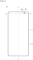
- FIG. 1 is a view illustrating a front side of an electronic device 20 including a display 10 according to various embodiments.
- the electronic device 20 including the display 10 is illustrated.
- the electronic device 20 may include a housing 22 and the display 10 provided inside the housing 22.
- a display area 21 of the electronic device may refer to an area where a screen is displayed by pixels and may correspond to an active area of the display 10 disposed inside the housing of the electronic device 20.
- the display area 21 may be formed on at least part of a front part of the housing 22.
- the display area 21 may be formed on the entire front part of the housing 22.
- An opening having a shape corresponding to the display area 21 may be formed in the front part of the housing 22.
- the display 10 provided inside the housing 22 may be disposed so as to be exposed.
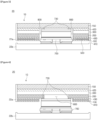
- a transparent layer 150 of the display 10 may be formed at the opening of the front part of the housing 22. Through the transparent layer of the display 10, the screen of the display 10 may be displayed on the front side of the electronic device 20. Furthermore, a sensor 700 mounted in the display may be exposed through the front side.
- the sensor 700 may be mounted in an opening 800 formed in the active area of the display 10. An upper surface of the sensor 700 may be disposed to face the transparent layer 150.
- the sensor 700 may be an optical sensor capable of receiving external light passing through the transparent layer 150.
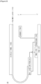
- the module-flexible printed circuit board 24 may be electrically connected with a partial area of the polymer layer 110.
- the module-flexible printed circuit board 24 may be electrically connected with a conductive pattern (or, wiring) formed on the polymer layer 110.
- the module-flexible printed circuit board 24 may be referred to as the M-FPCB (module-flexible printed circuit board).
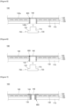
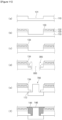
- the opening 800 may include at least one step portion.
- the first step portion may be formed by the organic light emitting layer 130 and the thin film encapsulation layer 140.
- the first step portion may include the first step surface 134, and the first step surface 134 may be formed toward the front part of the housing 22.
- the moisture barrier 146 may be disposed on the upper surface of the sensor 700.
- the moisture barrier 146 may block a path along which moisture infiltrates.
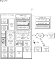
- the processor 1220 may include a main processor 1221 (e.g., a central processing unit or an application processor) and an auxiliary processor 1223 (e.g., a graphic processing device, an image signal processor, a sensor hub processor, or a communication processor), which operates independently from the main processor 1221 or with the main processor 1221. Additionally or alternatively, the auxiliary processor 1223 may use less power than the main processor 1221, or is specified to a designated function. The auxiliary processor 1223 may be implemented separately from the main processor 1221 or as a part thereof.
- a main processor 1221 e.g., a central processing unit or an application processor
- auxiliary processor 1223 e.g., a graphic processing device, an image signal processor, a sensor hub processor, or a communication processor
- the auxiliary processor 1223 may use less power than the main processor 1221, or is specified to a designated function.
- the auxiliary processor 1223 may be implemented separately from the main processor 1221 or as a part thereof.
- the auxiliary processor1223 may control, for example, at least some of functions or states associated with at least one component (e.g., the display device 1260, the sensor module 1276, or the communication module 1290) among the components of the electronic device 1201 instead of the main processor 1221 while the main processor 1221 is in an inactive (e.g., sleep) state or together with the main processor 1221 while the main processor 1221 is in an active (e.g., an application execution) state.
- the auxiliary processor1223 e.g., the image signal processor or the communication processor
- the memory 1230 may store a variety of data used by at least one component (e.g., the processor 1220 or the sensor module 1276) of the electronic device 1201.
- data may include software (e.g., the program 1240) and input data or output data with respect to commands associated with the software.
- the memory 1230 may include the volatile memory 1232 or the nonvolatile memory 1234.
- the program 1240 may be stored in the memory 1230 as software and may include, for example, an operating system 1242, a middleware 1244, or an application 1246.
- the input device 1250 may receive a command or data, which is used for a component (e.g., the processor 1220) of the electronic device 1201, from an outside (e.g., a user) of the electronic device 1201.
- the input device 1250 may include, for example, a microphone, a mouse, a keyboard, or a digital pen (e.g., a stylus pen).
- the sound output device 1255 may output a sound signal to the outside of the electronic device 1201.
- the sound output device 1255 may include, for example, a speaker or a receiver.
- the speaker may be used for general purposes, such as multimedia play or recordings play, and the receiver may be used for receiving calls. According to an embodiment, the receiver and the speaker may be either integrally or separately implemented.
- the display device 1260 may visually provide information to the outside (e.g., the user) of the electronic device 1201.
- the display device 1260 may include a display, a hologram device, or a projector and a control circuit for controlling a corresponding device.
- the display device 1260 may include a touch circuitry configured to sense the touch or a sensor circuit (e.g., a pressure sensor) for measuring an intensity of pressure on the touch.
- the audio module 1270 may convert a sound and an electrical signal in dual directions. According to an embodiment, the audio module 1270 may obtain the sound through the input device 1250 or may output the sound through the sound output device 1255or an external electronic device (e.g., the electronic device 1202 (e.g., a speaker or a headphone)) directly or wirelessly connected to the electronic device 1201.
- an external electronic device e.g., the electronic device 1202 (e.g., a speaker or a headphone) directly or wirelessly connected to the electronic device 1201.
- the sensor module 1276 may generate an electrical signal or a data value corresponding to an operating state (e.g., power or temperature) inside or an environmental state (e.g., a user state) outside the electronic device 1201.
- the sensor module 1276 may include, for example, a gesture sensor, a gyro sensor, a barometric pressure sensor, a magnetic sensor, an acceleration sensor, a grip sensor, a proximity sensor, a color sensor, an infrared sensor, a biometric sensor, a temperature sensor, a humidity sensor, or an illuminance sensor.
- the interface 1277 may support one or more designated protocols to allow the electronic device 1201 to connect directly or wirelessly to the external electronic device (e.g., the electronic device 1202).
- the interface 1277 may include, for example, an HDMI (high-definition multimedia interface), a USB (universal serial bus) interface, an SD card interface, or an audio interface.
- a connecting terminal1278 may include a connector that physically connects the electronic device 1201 to the external electronic device (e.g., the electronic device 1202).
- the connecting terminal 1278 may include, for example, an HDMI connector, a USB connector, an SD card connector, or an audio connector (e.g., a headphone connector).
- the haptic module 1279 may convert an electrical signal to a mechanical stimulation (e.g., vibration or movement) or an electrical stimulation perceived by the user through tactile or kinesthetic sensations.
- the haptic module 1279 may include, for example, a motor, a piezoelectric element, or an electric stimulator.
- the camera module 1280 may shoot a still image or a video image.
- the camera module 1280 may include, for example, at least one or more lenses, image sensors, image signal processors, or flashes.
- the power management module 1288 may manage power supplied to the electronic device 1201. According to an embodiment, the power management module 1288 may be implemented as at least a part of a power management integrated circuit (PMIC).
- PMIC power management integrated circuit
- the battery 1289 may supply power to at least one component of the electronic device 1201.
- the battery 1289 may include, for example, a non-rechargeable (primary) battery, a rechargeable (secondary) battery, or a fuel cell.
- the communication module 1290 may establish a direct (e.g., wired) or wireless communication channel between the electronic device 1201 and the external electronic device (e.g., the electronic device 1202, the electronic device 1204, or the server 1208) and support communication execution through the established communication channel.
- the communication module 1290 may include at least one communication processor operating independently from the processor 1220 (e.g., the application processor) and supporting the direct (e.g., wired) communication or the wireless communication.
- the communication module 1290 may include a wireless communication module 1292 (e.g., a cellular communication module, a short-range wireless communication module, or a GNSS (global navigation satellite system) communication module) or a wired communication module 1294 (e.g., an LAN (local area network) communication module or a power line communication module).
- a wireless communication module 1292 e.g., a cellular communication module, a short-range wireless communication module, or a GNSS (global navigation satellite system) communication module
- a wired communication module 1294 e.g., an LAN (local area network) communication module or a power line communication module.
- the corresponding communication module among the above communication modules may communicate with the external electronic device through the first network 1298 (e.g., the short-range communication network such as a Bluetooth, a WiFi direct, or an IrDA (infrared data association)) or the second network 1299 (e.g., the long-distance wireless communication network such as a cellular network, an internet, or a computer network (e.g., LAN or WAN)).
- the first network 1298 e.g., the short-range communication network such as a Bluetooth, a WiFi direct, or an IrDA (infrared data association)
- the second network 1299 e.g., the long-distance wireless communication network such as a cellular network, an internet, or a computer network (e.g., LAN or WAN)
- the above-mentioned various communication modules may be implemented into one component (e.g., a single chip) or into separate components (e.g., chips), respectively.
- the wireless communication module 1292 may identify and authenticate the electronic device 1201using user information (e.g., international mobile subscriber identity (IMSI)) stored in the subscriber identification module 1296in the communication network, such as the first network 1298 or the second network 1299.
- user information e.g., international mobile subscriber identity (IMSI)
- IMSI international mobile subscriber identity
- the antenna module 1297 may transmit or receive a signal or power to or from the outside (e.g., an external electronic device).
- the antenna module 1297 may include one or more antennas.
- the communication module 1290 may select one antenna suitable for a communication method used in the communication network such as the first network 1298 or the second network 1299.
- the signal or power may be transmitted or received between the communication module 1290 and the external electronic device through the selected one antenna.
- At least some components among the components may be connected to each other through a communication method (e.g., a bus, a GPIO (general purpose input and output), an SPI (serial peripheral interface), or an MIPI (mobile industry processor interface)) used between peripheral devices to exchange signals (e.g., a command or data) with each other.
- a communication method e.g., a bus, a GPIO (general purpose input and output), an SPI (serial peripheral interface), or an MIPI (mobile industry processor interface) used between peripheral devices to exchange signals (e.g., a command or data) with each other.
- the command or data may be transmitted or received between the electronic device 1201 and the external electronic device 1204 through the server 1208 connected to the second network 1299.
- Each of the electronic devices 1202 and 1204 may be the same or different types as or from the electronic device 1201.
- all or some of the operations performed by the electronic device 1201 may be performed by one or more external electronic devices among the external electronic devices 1202, 1204, or 1208.
- the electronic device 1201 may request one or more external electronic devices to perform at least some of the functions related to the functions or services, in addition to or instead of performing the functions or services by itself.
- the one or more external electronic devices receiving the request may carry out at least a part of the requested function or service or the additional function or service associated with the request and transmit the execution result to the electronic device 1201.
- the electronic device 1201 may provide the result as is or after additional processing as at least a part of the response to the request.
- a cloud computing, distributed computing, or client-server computing technology may be used.
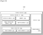
- FIG. 13 is a block diagram 1300 of the display device 1260 according to various embodiments.
- the display device 1260 may include a display 1310 and a display driver IC (DDI) 1330 for controlling the display 1310.
- the DDI 1330 may include an interface module 1331, a memory 1333 (e.g., a buffer memory), an image processing module 1335, or a mapping module 1337.
- the DDI 1330 may receive, for example, image data or image information including an image control signal corresponding to an instruction for controlling the image data, from another component of the electronic device 1201 through the interface module 1331.
- the image information may be received from the processor 1220 (e.g., the main processor 1221 (e.g., an application processor) or the auxiliary processor 1223 (e.g., a graphic processing device) that operates independently of a function of the main processor 1221).
- the DDI 1330 may communicate with touch circuitry 1350, the sensor module 1276, or the like through the interface module 1331.
- the DDI 1330 may store at least part of the received image information in the memory 1333, for example, on a frame-by-frame basis.
- the image processing module 1335 may pre-process or post-process at least part of the image data (e.g., may adjust the resolution, brightness, or size thereof), based at least on characteristics of the image data or characteristics of the display 1310.
- the mapping module 1337 may generate a voltage value or a current value that corresponds to the image data pre-processed or post-processed through the image processing module 1235. According to an embodiment, the generation of the voltage value or the current value may be performed based at least partly on, for example, attributes of pixels of the display 1310 (e.g., an arrangement of the pixels (an RGB stripe or pentile structure) or the size of each of sub-pixels).
- At least some pixels of the display 1310 may be driven based at least partly on, for example, the voltage value or the current value, and therefore visual information (e.g., text, an image, or an icon) that corresponds to the image data may be displayed through the display 1310.
- visual information e.g., text, an image, or an icon
- the display device 1260 may further include the touch circuitry 1350.
- the touch circuitry 1350 may include a touch sensor 1351 and a touch sensor IC 1353 for controlling the touch sensor 1351.
- the touch sensor IC 1353 may control the touch sensor 1351 to detect, for example, a touch input or a hovering input to a specific position of the display 1310.
- the touch sensor IC 1353 may detect the touch input or the hovering input by measuring a change of a signal (e.g., voltage, an amount of light, resistance, or an amount of electric charge) for the specific position of the display 1310.
- the touch sensor IC 1353 may provide information (e.g., position, area, pressure, or time) regarding the detected touch input or hovering input to the processor 1220.
- At least a part (e.g., the touch sensor IC 1353) of the touch circuitry 1350 may be included as a part of the display driver IC 1330 or the display 1310 or a part of another component (e.g., the auxiliary processor 1223) that is disposed outside the display device 1260.
- the display device 1260 may further include at least one sensor (e.g., a fingerprint sensor, an iris sensor, a pressure sensor, or an illuminance sensor) of the sensor module 1276 or control circuitry for the at least one sensor.
- the at least one sensor or the control circuitry for the same may be embedded in a part (e.g., the display 1310 or the DDI 1330) of the display device 1260 or a part of the touch circuitry 1350.
- the biometric sensor may obtain biometric information (e.g., a fingerprint image) associated with a touch input, through a partial area of the display 1310.
- the sensor module 1276 embedded in the display device 1260 includes a pressure sensor
- the pressure sensor may obtain pressure information associated with a touch input, through all or part of the display 1310.
- the touch sensor 1351 or the sensor module 1276 may be disposed between pixels in a pixel layer of the display 1310, or over or under the pixel layer.
- the electronic device may be various types of devices.
- the electronic device may include, for example, a portable communication device (e.g., a smartphone), a computer device, a portable multimedia device, a mobile medical appliance, a camera, a wearable device, or a home appliance.
- a portable communication device e.g., a smartphone
- a computer device e.g
- each of the expressions "A or B”, “at least one of A and B”, “at least one of A or B”, “A, B, or C”, “one or more of A, B, and C", or “one or more of A, B, or C”, and the like used herein may include any and all combinations of one or more of the associated listed items.
- the expressions, such as “a first”, “a second”, “the first”, or “the second”, may be used merely for the purpose of distinguishing a component from the other components, but do not limit the corresponding components in other aspect (e.g., the importance or the order).
- an element e.g., a first element
- the element may be coupled with the other element directly (e.g., wiredly), wirelessly, or via a third element.
- module used in the disclosure may include a unit implemented in hardware, software, or firmware and may be interchangeably used with the terms “logic”, “logical block”, “part” and “circuit”.
- the “module” may be a minimum unit of an integrated part or may be a part thereof.
- the “module” may be a minimum unit for performing one or more functions or a part thereof.
- the “module” may include an application-specific integrated circuit (ASIC).
- ASIC application-specific integrated circuit
- Various embodiments of the disclosure may be implemented by software (e.g., the program 1240) including an instruction stored in a machine-readable storage medium (e.g., an internal memory 1236 or an external memory 1238) readable by a machine (e.g., the electronic device 1201).
- a machine e.g., the electronic device 1201
- the processor e.g., the processor1220
- the machine may call the instruction from the machine-readable storage medium and execute the instructions thus called. This means that the machine may perform at least one function based on the called at least one instruction.
- the one or more instructions may include a code generated by a compiler or executable by an interpreter.
- the machine-readable storage medium may be provided in the form of non-transitory storage medium.
- non-transitory means that the storage medium is tangible, but does not include a signal (e.g., an electromagnetic wave).
- a signal e.g., an electromagnetic wave.
- non-transitory does not differentiate a case where the data is permanently stored in the storage medium from a case where the data is temporally stored in the storage medium.
- the method according to various embodiments disclosed in the disclosure may be provided as a part of a computer program product.
- the computer program product may be traded between a seller and a buyer as a product.
- the computer program product may be distributed in the form of machine-readable storage medium (e.g., a compact disc read only memory (CD-ROM)) or may be directly distributed (e.g., download or upload) online through an application store (e.g., a Play Store TM ) or between two user devices (e.g., the smartphones).
- an application store e.g., a Play Store TM
- at least a portion of the computer program product may be temporarily stored or generated in a machine-readable storage medium such as a memory of a manufacturer's server, an application store's server, or a relay server.
- each component e.g., the module or the program of the above-described components may include one or plural entities. According to various embodiments, at least one or more components of the above components or operations may be omitted, or one or more components or operations may be added. Alternatively or additionally, some components (e.g., the module or the program) may be integrated in one component. In this case, the integrated component may perform the same or similar functions performed by each corresponding components prior to the integration. According to various embodiments, operations performed by a module, a programming, or other components may be executed sequentially, in parallel, repeatedly, or in a heuristic method, or at least some operations may be executed in different sequences, omitted, or other operations may be added.
Landscapes
- Engineering & Computer Science (AREA)
- Signal Processing (AREA)
- Chemical & Material Sciences (AREA)
- Inorganic Chemistry (AREA)
- Physics & Mathematics (AREA)
- Optics & Photonics (AREA)
- Microelectronics & Electronic Packaging (AREA)
- Life Sciences & Earth Sciences (AREA)
- Sustainable Development (AREA)
- Geometry (AREA)
- Electroluminescent Light Sources (AREA)
- Devices For Indicating Variable Information By Combining Individual Elements (AREA)
Claims (13)
- Anzeige (10, 1310), umfassend:eine Anzeigesubstratschicht (110);eine organische lichtemittierende Schicht (130), die über der Anzeigesubstratschicht (110) ausgebildet ist, wobei die organische lichtemittierende Schicht (130) eine Vielzahl von Pixeln umfasst;eine Dünnschichttransistoranordnungsschicht (120), die zwischen der Anzeigesubstratschicht (110) und der organischen lichtemittierenden Schicht (130) angeordnet ist, wobei die Dünnschichttransistoranordnungsschicht (120) eine Vielzahl von Dünnschichttransistoren beinhaltet, die elektrisch mit den Pixeln verbunden sind;eine Dünnschichtverkapselungsschicht (140), die auf mindestens einem Teil der organischen lichtemittierenden Schicht (130) ausgebildet ist;ein Sensormontageteil, das eine Öffnung (800) umfasst, die durch die organische lichtemittierende Schicht, die Dünnschichttransistoranordnungsschicht (120) und die Anzeigesubstratschicht (110) ausgebildet ist, und einen Sensor (700), der in der Öffnung (800) angeordnet ist; gekennzeichnet durchein in der Öffnung (800) ausgebildetes Dichtungselement (142), um zu verhindern, dass die organische lichtemittierende Schicht (130) und die Dünnschichttransistoranordnungsschicht (120) durch eine innere Seitenwand der Öffnung (800) nach außen freiliegen,wobei die Öffnung (800) einen ersten Abschnitt, der in der Anzeigesubstratschicht (110) ausgebildet ist, und einen zweiten Abschnitt, der in dem Rest ausgebildet ist, umfasst,wobei die Öffnung (800) einen ersten stufenförmigen Abschnitt, der durch die organische lichtemittierende Schicht und die Dünnschichtverkapselungsschicht ausgebildet ist, und einen zweiten stufenförmigen Abschnitt, der auf der Anzeigesubstratschicht (110) ausgebildet ist, umfasst, undwobei das Dichtungselement (142) in dem zweiten Abschnitt und mindestens einem Teil des ersten Abschnitts ausgebildet ist.
- Anzeige (10, 1310) nach Anspruch 1, wobei das Dichtungselement (142) einen Füllstoff (144) umfasst, der zwischen der inneren Seitenwand der Öffnung (800) und dem Sensor (700) empfangen wird, und der Füllstoff (144) Epoxid und/oder ein Harz enthält.
- Anzeige (10, 1310) nach Anspruch 1, wobei die organische lichtemittierende Schicht (130) einen eingekapselten Bereich, auf dem die Dünnschichtverkapselungsschicht (140) ausgebildet ist, und einen freiliegenden Bereich umfasst, der sich von dem eingekapselten Bereich in einer Richtung zur Mitte der Öffnung (800) hin erstreckt, und
wobei das Dichtungselement (142) eine Sperrschicht (148) beinhaltet, die ausgebildet ist, um den freiliegenden Bereich abzudecken. - Anzeige (10, 1310) nach Anspruch 3, wobei der freiliegende Bereich eine erste stufenförmige Fläche beinhaltet, die auf einer Fläche der organischen lichtemittierenden Schicht (130) ausgebildet ist, und eine innere Seitenwand der organischen lichtemittierenden Schicht (130), die durch die Öffnung (800) ausgebildet ist, und die Sperrschicht (148) aus einem anorganischen Material und/oder einem metallischen Material ausgebildet ist.
- Anzeige (10, 1310) nach Anspruch 1, wobei die Dünnschichtverkapselungsschicht (140) eine auf der organischen lichtemittierenden Schicht (130) ausgebildete erste Schicht und eine auf der ersten Schicht ausgebildete zweite Schicht umfasst, und
wobei die erste Schicht aus einem organischen Material und/oder einem anorganischen Material ausgebildet ist, und die zweite Schicht aus einem anorganischen Material ausgebildet ist. - Anzeige (10, 1310) nach Anspruch 1, wobei die Anzeigesubstratschicht (110) aus einer Polymerschicht ausgebildet ist, die Polyimid enthält.
- Anzeige (10, 1310) nach Anspruch 1, wobei das Dichtungselement (142) mit der Dünnschichtverkapselungsschicht (140) verbunden ist.
- Anzeige (10, 1310) nach Anspruch 1, wobei sich das Dichtungselement (142) von der Dünnschichtverkapselungsschicht (140) aus erstreckt.
- Anzeige (10, 1310) nach Anspruch 8, wobei das Dichtungselement (142) und die Dünnschichtverkapselungsschicht (140) aus dem gleichen Material ausgebildet sind.
- Anzeige (10, 1310) nach Anspruch 9, wobei das Dichtungselement (142) ferner einen verbleibenden Teil der inneren Seitenwand der Öffnung (800) abdeckt, die durch die organische lichtemittierende Schicht (130) und die Dünnschichttransistoranordnungsschicht (120) ausgebildet ist.
- Anzeige (10, 1310) nach Anspruch 1, wobei der Sensor (700) eine Kamera umfasst.
- Anzeige (10, 1310) nach Anspruch 1, wobei die Anzeige eine Feuchtigkeitssperre (146) umfasst, die über dem Sensor (700) angeordnet ist, um die Einwirkung von Feuchtigkeit auf den Sensor (700) zu unterbrechen.
- Anzeige nach Anspruch 12, wobei sich die Feuchtigkeitssperre (146) in einer Richtung zur Außenseite des Sensors (700) hin erstreckt und mit der Dünnschichtverkapselungsschicht (140) verbunden ist.
Applications Claiming Priority (2)
| Application Number | Priority Date | Filing Date | Title |
|---|---|---|---|
| KR1020180008286A KR102443229B1 (ko) | 2018-01-23 | 2018-01-23 | 센서를 장착하기 위한 개구를 포함하는 디스플레이 |
| PCT/KR2019/000950 WO2019147012A1 (ko) | 2018-01-23 | 2019-01-23 | 센서를 장착하기 위한 개구를 포함하는 디스플레이 |
Publications (4)
| Publication Number | Publication Date |
|---|---|
| EP3720103A1 EP3720103A1 (de) | 2020-10-07 |
| EP3720103A4 EP3720103A4 (de) | 2021-05-05 |
| EP3720103C0 EP3720103C0 (de) | 2025-07-02 |
| EP3720103B1 true EP3720103B1 (de) | 2025-07-02 |
Family
ID=67395525
Family Applications (1)
| Application Number | Title | Priority Date | Filing Date |
|---|---|---|---|
| EP19743306.3A Active EP3720103B1 (de) | 2018-01-23 | 2019-01-23 | Anzeige mit öffnung zur montage eines sensors |
Country Status (6)
| Country | Link |
|---|---|
| US (1) | US11482692B2 (de) |
| EP (1) | EP3720103B1 (de) |
| KR (1) | KR102443229B1 (de) |
| CN (1) | CN111630831B (de) |
| AU (1) | AU2019210937B2 (de) |
| WO (1) | WO2019147012A1 (de) |
Families Citing this family (36)
| Publication number | Priority date | Publication date | Assignee | Title |
|---|---|---|---|---|
| US10270033B2 (en) | 2015-10-26 | 2019-04-23 | Oti Lumionics Inc. | Method for patterning a coating on a surface and device including a patterned coating |
| CN110301053B (zh) | 2016-12-02 | 2024-05-10 | Oti照明公司 | 包括设置在发射区域上面的导电涂层的器件及其方法 |
| CN116583131A (zh) | 2017-04-26 | 2023-08-11 | Oti照明公司 | 用于图案化表面上覆层的方法和包括图案化覆层的装置 |
| JP7264488B2 (ja) | 2017-05-17 | 2023-04-25 | オーティーアイ ルミオニクス インコーポレーテッド | パターン化コーティングにわたって伝導性コーティングを選択的に堆積させるための方法および伝導性コーティングを含むデバイス |
| CN108321176B (zh) * | 2018-02-02 | 2020-07-03 | 京东方科技集团股份有限公司 | 一种柔性显示面板、其制作方法及显示装置 |
| US11751415B2 (en) | 2018-02-02 | 2023-09-05 | Oti Lumionics Inc. | Materials for forming a nucleation-inhibiting coating and devices incorporating same |
| JP2022508040A (ja) | 2018-11-23 | 2022-01-19 | オーティーアイ ルミオニクス インコーポレーテッド | 光透過領域を含むオプトエレクトロニクスデバイス |
| CN109445007B (zh) * | 2019-01-02 | 2021-04-23 | 京东方科技集团股份有限公司 | 一种光学膜、显示屏组件及显示装置 |
| JP7390739B2 (ja) | 2019-03-07 | 2023-12-04 | オーティーアイ ルミオニクス インコーポレーテッド | 核生成抑制コーティングを形成するための材料およびそれを組み込んだデバイス |
| KR102831863B1 (ko) | 2019-04-18 | 2025-07-10 | 오티아이 루미오닉스 인크. | 핵 생성 억제 코팅 형성용 물질 및 이를 포함하는 디바이스 |
| JP7576337B2 (ja) | 2019-05-08 | 2024-11-01 | オーティーアイ ルミオニクス インコーポレーテッド | 核生成抑制コーティングを形成するための材料およびそれを組み込んだデバイス |
| CN114097102B (zh) | 2019-06-26 | 2023-11-03 | Oti照明公司 | 包括具有光衍射特征的光透射区域的光电设备 |
| US11832473B2 (en) | 2019-06-26 | 2023-11-28 | Oti Lumionics Inc. | Optoelectronic device including light transmissive regions, with light diffraction characteristics |
| CN114342068A (zh) | 2019-08-09 | 2022-04-12 | Oti照明公司 | 包含辅助电极和分区的光电子装置 |
| CN110571351B (zh) * | 2019-08-14 | 2021-01-15 | 武汉华星光电半导体显示技术有限公司 | 柔性显示面板结构及制作方法 |
| CN110311061B (zh) * | 2019-08-14 | 2021-10-15 | 京东方科技集团股份有限公司 | 显示装置、显示面板及其制备方法 |
| KR102837745B1 (ko) * | 2019-08-28 | 2025-07-24 | 엘지이노텍 주식회사 | 광학 기기 |
| KR20260036028A (ko) | 2019-12-24 | 2026-03-13 | 오티아이 루미오닉스 인크. | 캡핑 층을 포함하는 발광 장치 및 그 제조방법 |
| KR102899769B1 (ko) * | 2019-12-31 | 2025-12-12 | 엘지디스플레이 주식회사 | 표시 패널 및 이를 이용한 표시 장치 |
| KR102722363B1 (ko) * | 2020-02-04 | 2024-10-28 | 삼성전자주식회사 | 부품 적층 실장 구조 및 이를 포함하는 전자 장치 |
| KR102736680B1 (ko) | 2020-02-10 | 2024-12-02 | 삼성전자 주식회사 | 디스플레이 아래에 카메라가 배치된 구조를 갖는 전자 장치 |
| KR20210105782A (ko) * | 2020-02-19 | 2021-08-27 | 삼성전자주식회사 | 디스플레이를 포함하는 전자 장치 |
| KR102796530B1 (ko) | 2020-02-19 | 2025-04-17 | 삼성디스플레이 주식회사 | 전자 장치 |
| KR20210109100A (ko) | 2020-02-26 | 2021-09-06 | 삼성디스플레이 주식회사 | 전자 장치 |
| KR102717061B1 (ko) | 2020-03-06 | 2024-10-16 | 삼성디스플레이 주식회사 | 전자 장치 |
| CN111405791B (zh) | 2020-03-30 | 2021-05-18 | 维沃移动通信有限公司 | 电子设备 |
| KR102811194B1 (ko) | 2020-04-21 | 2025-05-22 | 삼성전자주식회사 | 광학 센서를 포함하는 전자 장치 |
| CN211743161U (zh) * | 2020-04-24 | 2020-10-23 | 京东方科技集团股份有限公司 | 一种显示基板和显示装置 |
| KR20210132497A (ko) * | 2020-04-27 | 2021-11-04 | 삼성전자주식회사 | 센서를 포함하는 전자 장치 |
| US12113279B2 (en) | 2020-09-22 | 2024-10-08 | Oti Lumionics Inc. | Device incorporating an IR signal transmissive region |
| CN112289840B (zh) * | 2020-10-30 | 2022-12-13 | 天马微电子股份有限公司 | 显示装置 |
| CN112736117B (zh) * | 2020-12-23 | 2024-04-26 | 深圳市华星光电半导体显示技术有限公司 | 显示面板 |
| CN113687534B (zh) | 2021-08-25 | 2022-08-05 | 武汉华星光电技术有限公司 | 显示面板及显示装置 |
| KR102837376B1 (ko) * | 2021-11-16 | 2025-07-22 | 엘지디스플레이 주식회사 | 표시 장치 |
| US12527201B2 (en) | 2021-12-29 | 2026-01-13 | Lg Display Co., Ltd. | Display apparatus |
| WO2026043499A1 (en) * | 2024-08-23 | 2026-02-26 | Harman International Industries, Incorporated | Display apparatus and integrated camera system having display apparatus |
Family Cites Families (20)
| Publication number | Priority date | Publication date | Assignee | Title |
|---|---|---|---|---|
| US6734463B2 (en) * | 2001-05-23 | 2004-05-11 | Semiconductor Energy Laboratory Co., Ltd. | Semiconductor device comprising a window |
| JP4355652B2 (ja) * | 2004-12-27 | 2009-11-04 | 埼玉日本電気株式会社 | 電子機器及びその防塵構造 |
| US7933122B2 (en) * | 2007-06-06 | 2011-04-26 | Otter Products, Llc | Protective enclosure for a computer |
| US9035545B2 (en) | 2010-07-07 | 2015-05-19 | Lg Chem, Ltd. | Organic light emitting device comprising encapsulating structure |
| DE102011089443B4 (de) * | 2011-02-14 | 2016-12-01 | Lg Display Co., Ltd. | Anzeigevorrichtung |
| KR101813459B1 (ko) * | 2011-06-24 | 2018-01-02 | 엘지디스플레이 주식회사 | 디스플레이 장치 |
| KR101406129B1 (ko) * | 2012-03-28 | 2014-06-13 | 엘지디스플레이 주식회사 | 디스플레이 장치 |
| US9214507B2 (en) * | 2012-08-17 | 2015-12-15 | Apple Inc. | Narrow border organic light-emitting diode display |
| KR102006775B1 (ko) * | 2012-08-30 | 2019-08-02 | 엘지디스플레이 주식회사 | 액정패널 및 이를 이용한 액정표시장치 |
| KR102102911B1 (ko) * | 2013-11-29 | 2020-04-21 | 엘지디스플레이 주식회사 | 유기발광표시장치 및 그의 제조방법 |
| JP2016019102A (ja) * | 2014-07-07 | 2016-02-01 | 株式会社 共栄精機 | スマートフォン用保護フィルム貼付補助具 |
| FR3033458B1 (fr) | 2015-03-05 | 2018-06-15 | Moteurs Leroy-Somer | Ensemble electromecanique comportant un alternateur |
| CN104867961B (zh) * | 2015-04-24 | 2020-06-30 | 京东方科技集团股份有限公司 | 阵列基板、其制造方法及显示装置 |
| CN104882569B (zh) | 2015-06-24 | 2017-01-25 | 京东方科技集团股份有限公司 | Oled显示器件及其制备方法、显示面板和显示装置 |
| KR102552272B1 (ko) | 2015-11-20 | 2023-07-07 | 삼성디스플레이 주식회사 | 유기 발광 표시 장치 및 그 제조 방법 |
| KR102501111B1 (ko) * | 2015-12-28 | 2023-02-16 | 엘지디스플레이 주식회사 | 카메라 모듈 일체형 액정 표시 장치 및 그 제조 방법 |
| KR102460423B1 (ko) | 2016-02-19 | 2022-10-31 | 삼성전자주식회사 | 전자 장치 |
| KR20170111827A (ko) * | 2016-03-29 | 2017-10-12 | 삼성전자주식회사 | 디스플레이 및 카메라를 포함하는 전자 장치 |
| US10741621B2 (en) * | 2016-11-25 | 2020-08-11 | Lg Display Co., Ltd. | Display device with a fingerprint sensor |
| KR102682304B1 (ko) * | 2016-12-02 | 2024-07-08 | 삼성전자주식회사 | 디스플레이를 포함하는 전자 장치 및 디스플레이의 제조 방법 |
-
2018
- 2018-01-23 KR KR1020180008286A patent/KR102443229B1/ko active Active
-
2019
- 2019-01-23 WO PCT/KR2019/000950 patent/WO2019147012A1/ko not_active Ceased
- 2019-01-23 EP EP19743306.3A patent/EP3720103B1/de active Active
- 2019-01-23 AU AU2019210937A patent/AU2019210937B2/en active Active
- 2019-01-23 CN CN201980009290.7A patent/CN111630831B/zh active Active
- 2019-01-23 US US16/961,831 patent/US11482692B2/en active Active
Also Published As
| Publication number | Publication date |
|---|---|
| US11482692B2 (en) | 2022-10-25 |
| KR102443229B1 (ko) | 2022-09-15 |
| AU2019210937B2 (en) | 2021-04-29 |
| EP3720103C0 (de) | 2025-07-02 |
| EP3720103A4 (de) | 2021-05-05 |
| KR20190089578A (ko) | 2019-07-31 |
| AU2019210937A1 (en) | 2020-07-23 |
| CN111630831B (zh) | 2023-08-15 |
| WO2019147012A1 (ko) | 2019-08-01 |
| EP3720103A1 (de) | 2020-10-07 |
| CN111630831A (zh) | 2020-09-04 |
| US20210083227A1 (en) | 2021-03-18 |
Similar Documents
| Publication | Publication Date | Title |
|---|---|---|
| EP3720103B1 (de) | Anzeige mit öffnung zur montage eines sensors | |
| US11429154B2 (en) | Electronic device including sensor for generating image data using incident light through opening formed in display | |
| US11531441B2 (en) | Display having opaque member disposed in area surrounded by pixels and electronic apparatus having the same | |
| US12174670B2 (en) | Flexible display and electronic device having same | |
| EP3678116A1 (de) | Anzeige mit gekrümmtem bereich und elektronische vorrichtung damit | |
| US20190312090A1 (en) | Electronic device including bendable display | |
| US10939570B2 (en) | Display and electronic device including waterproof structure | |
| US11453201B2 (en) | Window glass and electronic device including the same | |
| KR20210105782A (ko) | 디스플레이를 포함하는 전자 장치 | |
| KR20210099822A (ko) | 이미지 센서를 포함하는 전자 장치 | |
| US11088344B2 (en) | Display including filler member having separation space allowing light to be transmitted to optical adhesive member and electronic device including the same | |
| KR102832196B1 (ko) | 복수의 픽셀들에 의해 둘러싸인 영역에 형성된 불투명 부재를 포함하는 디스플레이 및 그를 갖는 전자 장치 | |
| US12364097B2 (en) | Electronic device comprising optical sensor and encapsulation layers | |
| KR102791590B1 (ko) | 더미 화소가 구비된 표시 패널을 포함하는 전자 장치 | |
| KR102498253B1 (ko) | 방수구조를 포함하는 디스플레이 및 전자 장치 | |
| KR20200101100A (ko) | 디스플레이 내에 배치된 센서에 인접한 픽셀들을 제어하기 위한 전자 장치 |
Legal Events
| Date | Code | Title | Description |
|---|---|---|---|
| STAA | Information on the status of an ep patent application or granted ep patent |
Free format text: STATUS: THE INTERNATIONAL PUBLICATION HAS BEEN MADE |
|
| PUAI | Public reference made under article 153(3) epc to a published international application that has entered the european phase |
Free format text: ORIGINAL CODE: 0009012 |
|
| STAA | Information on the status of an ep patent application or granted ep patent |
Free format text: STATUS: REQUEST FOR EXAMINATION WAS MADE |
|
| 17P | Request for examination filed |
Effective date: 20200703 |
|
| AK | Designated contracting states |
Kind code of ref document: A1 Designated state(s): AL AT BE BG CH CY CZ DE DK EE ES FI FR GB GR HR HU IE IS IT LI LT LU LV MC MK MT NL NO PL PT RO RS SE SI SK SM TR |
|
| AX | Request for extension of the european patent |
Extension state: BA ME |
|
| DAV | Request for validation of the european patent (deleted) | ||
| DAX | Request for extension of the european patent (deleted) | ||
| A4 | Supplementary search report drawn up and despatched |
Effective date: 20210401 |
|
| RIC1 | Information provided on ipc code assigned before grant |
Ipc: H04M 1/02 20060101AFI20210326BHEP Ipc: H01L 27/32 20060101ALI20210326BHEP Ipc: H01L 51/52 20060101ALI20210326BHEP |
|
| STAA | Information on the status of an ep patent application or granted ep patent |
Free format text: STATUS: EXAMINATION IS IN PROGRESS |
|
| 17Q | First examination report despatched |
Effective date: 20220614 |
|
| GRAP | Despatch of communication of intention to grant a patent |
Free format text: ORIGINAL CODE: EPIDOSNIGR1 |
|
| STAA | Information on the status of an ep patent application or granted ep patent |
Free format text: STATUS: GRANT OF PATENT IS INTENDED |
|
| RIC1 | Information provided on ipc code assigned before grant |
Ipc: H10K 77/10 20230101ALN20250116BHEP Ipc: H10K 59/80 20230101ALI20250116BHEP Ipc: H10K 59/65 20230101ALI20250116BHEP Ipc: H04M 1/02 20060101AFI20250116BHEP |
|
| INTG | Intention to grant announced |
Effective date: 20250129 |
|
| GRAS | Grant fee paid |
Free format text: ORIGINAL CODE: EPIDOSNIGR3 |
|
| GRAA | (expected) grant |
Free format text: ORIGINAL CODE: 0009210 |
|
| STAA | Information on the status of an ep patent application or granted ep patent |
Free format text: STATUS: THE PATENT HAS BEEN GRANTED |
|
| AK | Designated contracting states |
Kind code of ref document: B1 Designated state(s): AL AT BE BG CH CY CZ DE DK EE ES FI FR GB GR HR HU IE IS IT LI LT LU LV MC MK MT NL NO PL PT RO RS SE SI SK SM TR |
|
| REG | Reference to a national code |
Ref country code: GB Ref legal event code: FG4D |
|
| REG | Reference to a national code |
Ref country code: CH Ref legal event code: EP |
|
| REG | Reference to a national code |
Ref country code: DE Ref legal event code: R096 Ref document number: 602019071935 Country of ref document: DE |
|
| REG | Reference to a national code |
Ref country code: IE Ref legal event code: FG4D |
|
| U01 | Request for unitary effect filed |
Effective date: 20250710 |
|
| U07 | Unitary effect registered |
Designated state(s): AT BE BG DE DK EE FI FR IT LT LU LV MT NL PT RO SE SI Effective date: 20250716 |
|
| PG25 | Lapsed in a contracting state [announced via postgrant information from national office to epo] |
Ref country code: IS Free format text: LAPSE BECAUSE OF FAILURE TO SUBMIT A TRANSLATION OF THE DESCRIPTION OR TO PAY THE FEE WITHIN THE PRESCRIBED TIME-LIMIT Effective date: 20251102 |
|
| PGFP | Annual fee paid to national office [announced via postgrant information from national office to epo] |
Ref country code: GB Payment date: 20251222 Year of fee payment: 8 |
|
| PG25 | Lapsed in a contracting state [announced via postgrant information from national office to epo] |
Ref country code: NO Free format text: LAPSE BECAUSE OF FAILURE TO SUBMIT A TRANSLATION OF THE DESCRIPTION OR TO PAY THE FEE WITHIN THE PRESCRIBED TIME-LIMIT Effective date: 20251002 |
|
| PG25 | Lapsed in a contracting state [announced via postgrant information from national office to epo] |
Ref country code: HR Free format text: LAPSE BECAUSE OF FAILURE TO SUBMIT A TRANSLATION OF THE DESCRIPTION OR TO PAY THE FEE WITHIN THE PRESCRIBED TIME-LIMIT Effective date: 20250702 |
|
| PG25 | Lapsed in a contracting state [announced via postgrant information from national office to epo] |
Ref country code: GR Free format text: LAPSE BECAUSE OF FAILURE TO SUBMIT A TRANSLATION OF THE DESCRIPTION OR TO PAY THE FEE WITHIN THE PRESCRIBED TIME-LIMIT Effective date: 20251003 |
|
| PG25 | Lapsed in a contracting state [announced via postgrant information from national office to epo] |
Ref country code: CZ Free format text: LAPSE BECAUSE OF FAILURE TO SUBMIT A TRANSLATION OF THE DESCRIPTION OR TO PAY THE FEE WITHIN THE PRESCRIBED TIME-LIMIT Effective date: 20250702 |
|
| PG25 | Lapsed in a contracting state [announced via postgrant information from national office to epo] |
Ref country code: PL Free format text: LAPSE BECAUSE OF FAILURE TO SUBMIT A TRANSLATION OF THE DESCRIPTION OR TO PAY THE FEE WITHIN THE PRESCRIBED TIME-LIMIT Effective date: 20250702 |
|
| PG25 | Lapsed in a contracting state [announced via postgrant information from national office to epo] |
Ref country code: RS Free format text: LAPSE BECAUSE OF FAILURE TO SUBMIT A TRANSLATION OF THE DESCRIPTION OR TO PAY THE FEE WITHIN THE PRESCRIBED TIME-LIMIT Effective date: 20251002 |
|
| PG25 | Lapsed in a contracting state [announced via postgrant information from national office to epo] |
Ref country code: ES Free format text: LAPSE BECAUSE OF FAILURE TO SUBMIT A TRANSLATION OF THE DESCRIPTION OR TO PAY THE FEE WITHIN THE PRESCRIBED TIME-LIMIT Effective date: 20250702 |
|
| U20 | Renewal fee for the european patent with unitary effect paid |
Year of fee payment: 8 Effective date: 20260122 |
|
| PG25 | Lapsed in a contracting state [announced via postgrant information from national office to epo] |
Ref country code: SM Free format text: LAPSE BECAUSE OF FAILURE TO SUBMIT A TRANSLATION OF THE DESCRIPTION OR TO PAY THE FEE WITHIN THE PRESCRIBED TIME-LIMIT Effective date: 20250702 |
|
| PG25 | Lapsed in a contracting state [announced via postgrant information from national office to epo] |
Ref country code: SK Free format text: LAPSE BECAUSE OF FAILURE TO SUBMIT A TRANSLATION OF THE DESCRIPTION OR TO PAY THE FEE WITHIN THE PRESCRIBED TIME-LIMIT Effective date: 20250702 |