EP3723075A1 - Circuit de pixel et son procédé d'attaque, panneau d'affichage et dispositif d'affichage - Google Patents
Circuit de pixel et son procédé d'attaque, panneau d'affichage et dispositif d'affichage Download PDFInfo
- Publication number
- EP3723075A1 EP3723075A1 EP18847206.2A EP18847206A EP3723075A1 EP 3723075 A1 EP3723075 A1 EP 3723075A1 EP 18847206 A EP18847206 A EP 18847206A EP 3723075 A1 EP3723075 A1 EP 3723075A1
- Authority
- EP
- European Patent Office
- Prior art keywords
- transistor
- bias
- circuit
- terminal
- electrode
- Prior art date
- Legal status (The legal status is an assumption and is not a legal conclusion. Google has not performed a legal analysis and makes no representation as to the accuracy of the status listed.)
- Pending
Links
- 238000000034 method Methods 0.000 title claims abstract description 35
- 239000003990 capacitor Substances 0.000 claims description 36
- 238000010586 diagram Methods 0.000 description 24
- 230000000694 effects Effects 0.000 description 16
- 238000004519 manufacturing process Methods 0.000 description 6
- 206010047571 Visual impairment Diseases 0.000 description 5
- 229920001621 AMOLED Polymers 0.000 description 2
- 238000004458 analytical method Methods 0.000 description 2
- 238000005516 engineering process Methods 0.000 description 2
- 238000004020 luminiscence type Methods 0.000 description 2
- 239000000463 material Substances 0.000 description 2
- 239000004065 semiconductor Substances 0.000 description 2
- 239000003086 colorant Substances 0.000 description 1
- 238000005265 energy consumption Methods 0.000 description 1
- 230000001360 synchronised effect Effects 0.000 description 1
- 239000010409 thin film Substances 0.000 description 1
Images




Classifications
-
- G—PHYSICS
- G09—EDUCATION; CRYPTOGRAPHY; DISPLAY; ADVERTISING; SEALS
- G09G—ARRANGEMENTS OR CIRCUITS FOR CONTROL OF INDICATING DEVICES USING STATIC MEANS TO PRESENT VARIABLE INFORMATION
- G09G3/00—Control arrangements or circuits, of interest only in connection with visual indicators other than cathode-ray tubes
- G09G3/20—Control arrangements or circuits, of interest only in connection with visual indicators other than cathode-ray tubes for presentation of an assembly of a number of characters, e.g. a page, by composing the assembly by combination of individual elements arranged in a matrix no fixed position being assigned to or needed to be assigned to the individual characters or partial characters
- G09G3/22—Control arrangements or circuits, of interest only in connection with visual indicators other than cathode-ray tubes for presentation of an assembly of a number of characters, e.g. a page, by composing the assembly by combination of individual elements arranged in a matrix no fixed position being assigned to or needed to be assigned to the individual characters or partial characters using controlled light sources
- G09G3/30—Control arrangements or circuits, of interest only in connection with visual indicators other than cathode-ray tubes for presentation of an assembly of a number of characters, e.g. a page, by composing the assembly by combination of individual elements arranged in a matrix no fixed position being assigned to or needed to be assigned to the individual characters or partial characters using controlled light sources using electroluminescent panels
- G09G3/32—Control arrangements or circuits, of interest only in connection with visual indicators other than cathode-ray tubes for presentation of an assembly of a number of characters, e.g. a page, by composing the assembly by combination of individual elements arranged in a matrix no fixed position being assigned to or needed to be assigned to the individual characters or partial characters using controlled light sources using electroluminescent panels semiconductive, e.g. using light-emitting diodes [LED]
- G09G3/3208—Control arrangements or circuits, of interest only in connection with visual indicators other than cathode-ray tubes for presentation of an assembly of a number of characters, e.g. a page, by composing the assembly by combination of individual elements arranged in a matrix no fixed position being assigned to or needed to be assigned to the individual characters or partial characters using controlled light sources using electroluminescent panels semiconductive, e.g. using light-emitting diodes [LED] organic, e.g. using organic light-emitting diodes [OLED]
- G09G3/3225—Control arrangements or circuits, of interest only in connection with visual indicators other than cathode-ray tubes for presentation of an assembly of a number of characters, e.g. a page, by composing the assembly by combination of individual elements arranged in a matrix no fixed position being assigned to or needed to be assigned to the individual characters or partial characters using controlled light sources using electroluminescent panels semiconductive, e.g. using light-emitting diodes [LED] organic, e.g. using organic light-emitting diodes [OLED] using an active matrix
- G09G3/3233—Control arrangements or circuits, of interest only in connection with visual indicators other than cathode-ray tubes for presentation of an assembly of a number of characters, e.g. a page, by composing the assembly by combination of individual elements arranged in a matrix no fixed position being assigned to or needed to be assigned to the individual characters or partial characters using controlled light sources using electroluminescent panels semiconductive, e.g. using light-emitting diodes [LED] organic, e.g. using organic light-emitting diodes [OLED] using an active matrix with pixel circuitry controlling the current through the light-emitting element
-
- G—PHYSICS
- G09—EDUCATION; CRYPTOGRAPHY; DISPLAY; ADVERTISING; SEALS
- G09G—ARRANGEMENTS OR CIRCUITS FOR CONTROL OF INDICATING DEVICES USING STATIC MEANS TO PRESENT VARIABLE INFORMATION
- G09G2300/00—Aspects of the constitution of display devices
- G09G2300/04—Structural and physical details of display devices
- G09G2300/0421—Structural details of the set of electrodes
- G09G2300/0426—Layout of electrodes and connections
-
- G—PHYSICS
- G09—EDUCATION; CRYPTOGRAPHY; DISPLAY; ADVERTISING; SEALS
- G09G—ARRANGEMENTS OR CIRCUITS FOR CONTROL OF INDICATING DEVICES USING STATIC MEANS TO PRESENT VARIABLE INFORMATION
- G09G2300/00—Aspects of the constitution of display devices
- G09G2300/04—Structural and physical details of display devices
- G09G2300/0421—Structural details of the set of electrodes
- G09G2300/043—Compensation electrodes or other additional electrodes in matrix displays related to distortions or compensation signals, e.g. for modifying TFT threshold voltage in column driver
-
- G—PHYSICS
- G09—EDUCATION; CRYPTOGRAPHY; DISPLAY; ADVERTISING; SEALS
- G09G—ARRANGEMENTS OR CIRCUITS FOR CONTROL OF INDICATING DEVICES USING STATIC MEANS TO PRESENT VARIABLE INFORMATION
- G09G2300/00—Aspects of the constitution of display devices
- G09G2300/08—Active matrix structure, i.e. with use of active elements, inclusive of non-linear two terminal elements, in the pixels together with light emitting or modulating elements
- G09G2300/0809—Several active elements per pixel in active matrix panels
- G09G2300/0819—Several active elements per pixel in active matrix panels used for counteracting undesired variations, e.g. feedback or autozeroing
-
- G—PHYSICS
- G09—EDUCATION; CRYPTOGRAPHY; DISPLAY; ADVERTISING; SEALS
- G09G—ARRANGEMENTS OR CIRCUITS FOR CONTROL OF INDICATING DEVICES USING STATIC MEANS TO PRESENT VARIABLE INFORMATION
- G09G2300/00—Aspects of the constitution of display devices
- G09G2300/08—Active matrix structure, i.e. with use of active elements, inclusive of non-linear two terminal elements, in the pixels together with light emitting or modulating elements
- G09G2300/0809—Several active elements per pixel in active matrix panels
- G09G2300/0842—Several active elements per pixel in active matrix panels forming a memory circuit, e.g. a dynamic memory with one capacitor
-
- G—PHYSICS
- G09—EDUCATION; CRYPTOGRAPHY; DISPLAY; ADVERTISING; SEALS
- G09G—ARRANGEMENTS OR CIRCUITS FOR CONTROL OF INDICATING DEVICES USING STATIC MEANS TO PRESENT VARIABLE INFORMATION
- G09G2300/00—Aspects of the constitution of display devices
- G09G2300/08—Active matrix structure, i.e. with use of active elements, inclusive of non-linear two terminal elements, in the pixels together with light emitting or modulating elements
- G09G2300/088—Active matrix structure, i.e. with use of active elements, inclusive of non-linear two terminal elements, in the pixels together with light emitting or modulating elements using a non-linear two-terminal element
-
- G—PHYSICS
- G09—EDUCATION; CRYPTOGRAPHY; DISPLAY; ADVERTISING; SEALS
- G09G—ARRANGEMENTS OR CIRCUITS FOR CONTROL OF INDICATING DEVICES USING STATIC MEANS TO PRESENT VARIABLE INFORMATION
- G09G2310/00—Command of the display device
- G09G2310/02—Addressing, scanning or driving the display screen or processing steps related thereto
- G09G2310/0202—Addressing of scan or signal lines
- G09G2310/0216—Interleaved control phases for different scan lines in the same sub-field, e.g. initialization, addressing and sustaining in plasma displays that are not simultaneous for all scan lines
-
- G—PHYSICS
- G09—EDUCATION; CRYPTOGRAPHY; DISPLAY; ADVERTISING; SEALS
- G09G—ARRANGEMENTS OR CIRCUITS FOR CONTROL OF INDICATING DEVICES USING STATIC MEANS TO PRESENT VARIABLE INFORMATION
- G09G2310/00—Command of the display device
- G09G2310/02—Addressing, scanning or driving the display screen or processing steps related thereto
- G09G2310/0243—Details of the generation of driving signals
- G09G2310/0251—Precharge or discharge of pixel before applying new pixel voltage
-
- G—PHYSICS
- G09—EDUCATION; CRYPTOGRAPHY; DISPLAY; ADVERTISING; SEALS
- G09G—ARRANGEMENTS OR CIRCUITS FOR CONTROL OF INDICATING DEVICES USING STATIC MEANS TO PRESENT VARIABLE INFORMATION
- G09G2320/00—Control of display operating conditions
- G09G2320/02—Improving the quality of display appearance
- G09G2320/0233—Improving the luminance or brightness uniformity across the screen
-
- G—PHYSICS
- G09—EDUCATION; CRYPTOGRAPHY; DISPLAY; ADVERTISING; SEALS
- G09G—ARRANGEMENTS OR CIRCUITS FOR CONTROL OF INDICATING DEVICES USING STATIC MEANS TO PRESENT VARIABLE INFORMATION
- G09G2320/00—Control of display operating conditions
- G09G2320/02—Improving the quality of display appearance
- G09G2320/0257—Reduction of after-image effects
Definitions
- Embodiments of the present disclosure relate to a pixel circuit and a driving method thereof, a display panel and a display device.
- OLED display devices have advantages of self-luminescence, high contrast, low energy consumption, wide viewing angle, fast response, being capable to be used in a flexible panel, wide using temperature range, simple manufacture and so on, and have broad development prospects.
- OLED display panels can be widely used in devices with display functions, such as mobile phones, displays, notebook computers, digital cameras, instrumentations and so on.
- At least one embodiment of the present disclosure provides a pixel circuit, which comprises a light emitting component, a drive circuit, a first reset bias circuit, and a second reset bias circuit.
- a control terminal of the drive circuit is electrically connected to a data signal terminal and a second terminal of the first reset bias circuit, a first terminal of the drive circuit is electrically connected to a second terminal of the second reset bias circuit, and a second terminal of the drive circuit is electrically connected to the light emitting component;
- a control terminal of the first reset bias circuit is electrically connected to a first control terminal, and a first terminal of the first reset bias circuit is electrically connected to a first bias voltage terminal;
- a control terminal of the second reset bias circuit is electrically connected to a bias control terminal, and a first terminal of the second reset bias circuit is electrically connected to a second bias voltage terminal; and the first reset bias circuit and the second reset bias circuit are configured to reset the drive circuit and control the drive circuit to be in a bias state during a reset phase.
- the drive circuit comprises a drive transistor
- the first reset bias circuit comprises a first bias transistor
- the second reset bias circuit comprises a second bias transistor
- the control terminal of the drive circuit is a gate electrode of the drive transistor
- the first terminal of the drive circuit is a first electrode of the drive transistor
- the second terminal of the drive circuit is a second electrode of the drive transistor
- the first terminal of the first reset bias circuit is a first electrode of the first bias transistor
- the second terminal of the first reset bias circuit is a second electrode of the first bias transistor
- the control terminal of the first reset bias circuit is a gate electrode of the first bias transistor
- the first terminal of the second reset bias circuit is a first electrode of the second bias transistor
- the second terminal of the second reset bias circuit is a second electrode of the second bias transistor
- the control terminal of the second reset bias circuit is a gate electrode of the second bias transistor.
- the pixel circuit provided by an embodiment of the present disclosure further comprises a data write circuit and a storage circuit.
- the data write circuit is configured to write a data signal to the gate electrode of the drive transistor during a data writing phase; and the storage circuit is configured to store the data signal and maintain the data signal at the gate electrode of the drive transistor.
- the pixel circuit provided by an embodiment of the present disclosure further comprises a threshold compensation circuit.
- the threshold compensation circuit is configured to write a threshold compensation signal to the gate electrode of the drive transistor during the data writing phase.
- the threshold compensation circuit comprises a threshold compensation transistor
- the data write circuit comprises a data write transistor
- the storage circuit comprises a storage capacitor
- a first electrode of the threshold compensation transistor is electrically connected to a second electrode of the data write transistor
- a second electrode of the threshold compensation transistor and a gate electrode of the threshold compensation transistor are electrically connected with each other, and are electrically connected to the gate electrode of the drive transistor
- a first electrode of the data write transistor is electrically connected to the data signal terminal, and a gate electrode of the data write transistor is electrically connected to a second control terminal
- a first terminal of the storage capacitor is electrically connected to the first electrode of the drive transistor, and a second terminal of the storage capacitor is electrically connected to the gate electrode of the drive transistor.
- the pixel circuit provided by an embodiment of the present disclosure further comprises a voltage drop compensation circuit.
- the voltage drop compensation circuit is configured to write a reference voltage signal to the first electrode of the drive transistor during the data writing phase.
- the voltage drop compensation circuit comprises a voltage drop compensation transistor
- the storage circuit comprises a storage capacitor
- a first electrode of the voltage drop compensation transistor is electrically connected to a reference power terminal
- a second electrode of the voltage drop compensation transistor is electrically connected to the first electrode of the drive transistor
- a gate electrode of the voltage drop compensation transistor is electrically connected to a second control terminal
- a first terminal of the storage capacitor is electrically connected to the first electrode of the drive transistor, and a second terminal of the storage capacitor is electrically connected to the gate electrode of the drive transistor.
- the pixel circuit provided by an embodiment of the present disclosure further comprises a light emitting control circuit, the light emitting control circuit is configured to control the drive circuit to drive the light emitting component to emit light.
- the light emitting control circuit comprises a first control transistor and a second control transistor, a first electrode of the first control transistor is electrically connected to the second electrode of the drive transistor, a second electrode of the first control transistor is electrically connected to the light emitting component, and a gate electrode of the first control transistor is electrically connected to a third control terminal, and a first electrode of the second control transistor is electrically connected to a first power voltage terminal, a second electrode of the second control transistor is electrically connected to the first electrode of the drive transistor, and a gate electrode of the second control transistor is configured to receive a light emitting control signal.
- the gate electrode of the second control transistor is electrically connected to the third control terminal to receive the light emitting control signal
- the gate electrode of the second bias transistor is electrically connected to the first control terminal
- the first electrode of the second bias transistor is electrically connected to a reset voltage terminal
- the reset voltage terminal is the second bias voltage terminal
- the first control terminal is the bias control terminal.
- a signal output by the first bias voltage terminal is same as a signal output by the second bias voltage terminal.
- the second bias transistor is multiplexed into the second control transistor.
- the second bias transistor is an N-type transistor
- the gate electrode of the second bias transistor is electrically connected to the second control terminal
- the first power voltage terminal is the second bias voltage terminal
- the second control terminal is the bias control terminal
- At least one embodiment of the present disclosure further provides a display panel, which comprises any one of the above pixel circuits.
- At least one embodiment of the present disclosure further provides a display device, which comprises the above display panel.
- At least one embodiment of the present disclosure provides a driving method of any one of the above pixel circuits, which comprises: during the reset phase, resetting the drive circuit and controlling the drive circuit to be in the bias state; during a data writing phase, writing a data signal to the drive circuit; and during a light emitting phase, driving the light emitting component to emit light.
- the drive circuit comprises a drive transistor, the first reset bias circuit comprises a first bias transistor, and the second reset bias circuit comprises a second bias transistor;
- the resetting the drive circuit and controlling the drive circuit to be in a bias state comprises: writing a first bias voltage signal to a gate electrode of the drive transistor through the first bias transistor; and writing a second bias voltage signal to a first electrode of the drive transistor through the second bias transistor.
- the drive transistor is controlled to be in the bias state by a difference between the first bias voltage signal and the second bias voltage signal.
- the first bias voltage signal and the second bias voltage signal are same.
- a first electrode of the second bias transistor is electrically connected to a first power voltage terminal to receive a first power voltage signal, and the first power voltage signal is the second bias voltage signal.
- the driving method provided by an embodiment of the present disclosure further comprises: during the data writing phase, writing a threshold compensation signal to the gate electrode of the drive transistor through a threshold compensation circuit.
- the driving method provided by an embodiment of the present disclosure further comprises: during the data writing phase, writing a reference voltage signal to the first electrode of the drive transistor through a voltage drop compensation circuit.
- connection is not intended to define a physical connection or mechanical connection, but may include an electrical connection, directly or indirectly.
- "On,” “under,” “right,” “left” and the like are only used to indicate relative position relationship, and when the position of the object which is described is changed, the relative position relationship may be changed accordingly.
- OLED organic light emitting diode
- Each pixel on the OLED display panel is driven by a plurality of thin film transistors (TFTs), and TFT driving technology can improve display speed, contrast and brightness, and improve resolution.
- TFT thin film transistors
- the hysteresis effect of the TFT is an uncertainty presented based on the electrical characteristics of the TFT under a certain bias voltage, that is, a current flowing through the TFT is not only related to the current bias voltage, but also related to the state of the TFT at the previous moment.
- the hysteresis effect of the TFT is related to the gate dielectric of the TFT, the semiconductor material of the TFT and the interface state trap therebetween.
- the hysteresis effect of the TFT causes a short-term afterimage, and an image of a previous frame are generally remained in an image of a next frame, thereby affecting the display quality of the OLED display panel, and even causing display errors.
- At least one embodiment of the present disclosure provides a pixel circuit and a driving method thereof, a display panel and a display device.
- the drive circuit is allowed to be in a bias state during a reset phase, so that when an image is displayed, the drive circuit is changed from the bias state to a corresponding display state, a data voltage of a display image in a next frame is not affected by a data voltage of a display image in a previous frame, thereby ameliorating a short-term afterimage problem caused by the hysteresis effect, and improving the display quality of the display panel.
- the driving method of the pixel circuit may further perform a threshold compensation operation and a voltage drop compensation operation, thereby compensating for threshold voltage drift of the drive transistor and power voltage drop (IR drop) of the display panel, thereby improving display uniformity, and effectively improving the display effect of the display panel.
- a threshold compensation operation and a voltage drop compensation operation thereby compensating for threshold voltage drift of the drive transistor and power voltage drop (IR drop) of the display panel, thereby improving display uniformity, and effectively improving the display effect of the display panel.
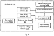
- Fig. 1 is a schematic block diagram of a pixel circuit provided by an embodiment of the present disclosure.
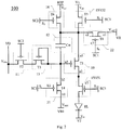
- Fig. 2 is a structural schematic diagram of a pixel circuit provided by an embodiment of the present disclosure.
- a pixel circuit 100 may comprise a light emitting component EL, a drive circuit 10, a first reset bias circuit 21, and a second reset bias circuit 22.
- a control terminal of the drive circuit 10 is respectively electrically connected to a data signal terminal VD and a second terminal of the first reset bias circuit 21, a first terminal of the drive circuit 10 is electrically connected to a second terminal of the second reset bias circuit 22, and a second terminal of the drive circuit 10 is electrically connected to the light emitting component EL.
- a control terminal of the first reset bias circuit 21 is electrically connected to a first control terminal SC1, a first terminal of the first reset bias circuit 21 is electrically connected to a first bias voltage terminal VB1.
- a control terminal of the second reset bias circuit 22 is electrically connected to a bias control terminal BS, and a first terminal of the second reset bias circuit 22 is electrically connected to a second bias voltage terminal VB2.
- the first reset bias circuit 21 and the second reset bias circuit 22 are configured to reset the drive circuit 10 and control the drive circuit 10 to be in a bias state during a reset phase.
- the pixel circuit 100 provided by the embodiment of the present disclosure can be applied to a display panel, such as an active matrix organic light emitting diode (AMOLED) display panel or the like.
- a display panel such as an active matrix organic light emitting diode (AMOLED) display panel or the like.
- AMOLED active matrix organic light emitting diode
- the light emitting component EL is configured to emit light when a voltage or current is applied thereto.
- the light emitting component EL can be an organic light emitting component, and the organic light emitting component can be, for example, an organic light emitting diode, but embodiments of the present disclosure are not limited thereto.
- the light emitting component EL can, for example, adopt different light emitting materials to emit light of different colors, so as to perform colorful luminescence.
- the drive circuit 10 the first reset bias circuit 21, and the second reset bias circuit 22 can be set according to actual application requirements, which are not specifically limited in the embodiments of the present disclosure.
- the pixel circuit 100 provided by the embodiments of the present disclosure can be implemented as a circuit structure illustrated in Fig. 2 .
- the drive circuit 10 comprises a drive transistor T1.
- the control terminal a3 of the drive circuit 10 is s gate electrode of the drive transistor T1
- the first terminal a1 of the drive circuit 10 is a first electrode of the drive transistor T1
- the second terminal a2 of the drive circuit 10 is a second electrode of the drive transistor T1.
- the drive circuit 10 being in a bias state may indicate that the drive transistor T1 is in a bias state, that is, the first reset bias circuit 21 and the second reset bias circuit 22 may control the drive transistor T1 to be in the bias state during the reset phase.
- the drive transistor T1 is a P-type transistor.
- the first electrode of the drive transistor T1 may be a source electrode, and the second electrode of the drive transistor T1 may be a drain electrode.
- "the drive transistor T1 being in a bias state” may indicate that a voltage difference between the gate electrode of the drive transistor T1 and the source electrode of the drive transistor T1 is not greater than a voltage difference Vgs255 between the gate electrode and the source electrode, in which Vgs255 corresponds to the maximum gray scale (ie, 255 gray scale).
- the Vgs (i.e., the voltage difference between the gate electrode of the drive transistor T1 and the source electrode of the drive transistor T1) of the drive transistor T1 is less than or equal to Vgs255.
- the drive transistor T1 being in a bias state may also indicate that the voltage difference between the gate electrode of the drive transistor T1 and the source electrode of the drive transistor T1 is not less than a threshold voltage V th1 of the drive transistor T1, that is, the Vgs of the drive transistor T1 is greater than or equal to V th1 .
- the first reset bias circuit 21 is configured to write a first bias voltage signal to the gate electrode of the drive transistor T1 during the reset phase; and the second reset bias circuit 22 is configured to write a second bias voltage signal to the first electrode of drive transistor T1 during the reset phase.
- a difference between the first bias voltage signal and the second bias voltage signal controls the drive transistor T1 to be in the bias state.
- the first bias voltage signal and the second bias voltage signal are respectively a gate voltage and a source voltage of the drive transistor T1, so that a voltage difference between the first bias voltage signal and the second bias voltage signal (For example, the voltage difference represents a difference obtained by subtracting the second bias voltage signal from the first bias voltage signal) is greater than or equal to V th1 ; alternatively, the voltage difference is less than or equal to Vgs255.
- the first reset bias circuit 21 comprises a first bias transistor T4.
- the first terminal b1 of the first reset bias circuit 21 is a first electrode of the first bias transistor T4
- the second terminal b2 of the first reset bias circuit 21 is a second electrode of the first bias transistor T4
- the control terminal b3 of the first reset bias circuit 21 is a gate electrode of the first bias transistor T4.
- the second reset bias circuit 22 comprises a second bias transistor T8.
- the first terminal c1 of the second reset bias circuit 22 is a first electrode of the second bias transistor T8, the second terminal c2 of the second reset bias circuit 22 is a second electrode of the second bias transistor T8, and the control terminal c3 of the second reset bias circuit 22 is a gate electrode of the second bias transistor T8.
- the first bias voltage terminal VB1 is configured to output a first bias voltage signal V init1
- the second bias voltage terminal VB2 is configured to output a second bias voltage signal V init2 .
- the gate electrode of the first bias transistor T4 is electrically connected to the first control terminal SC1 to receive a first control signal S 1
- the first electrode of the first bias transistor T4 is electrically connected to the first bias voltage terminal VB1 to receive the first bias voltage signal V init1
- the second electrode of the first bias transistor T4 is electrically connected to the gate electrode of the drive transistor T1 to transmit the first bias voltage signal V init1 to the gate electrode of the drive transistor T1 when the first bias transistor T4 is turned on.
- the gate electrode of the second bias transistor T8 is electrically connected to the first control terminal SC1
- the first electrode of the second bias transistor T8 is electrically connected to a reset voltage terminal VR
- the second electrode of the second bias transistor T8 is electrically connected to the first electrode of the drive transistor T1.
- the first control terminal SC1 is the bias control terminal BS
- the reset voltage terminal VR is the second bias voltage terminal VB2.
- the first control terminal SC1 can output the first control signal S 1
- the first control signal S 1 is a bias control signal.
- the reset voltage terminal VR can output the second bias voltage signal V init2 , and the first electrode of the second bias transistor T8 can receive the second bias voltage signal V init2 , so that the second bias voltage signal V init2 can be transmitted to the first electrode of the drive transistor T1 when the second bias transistor T8 is turned on.
- a type of the first bias transistor T4 and a type of the second bias transistor T8 are same.
- the first bias transistor T4 and the second bias transistor T8, for example, are both P-type transistors, and the gate electrode of the first bias transistor T4 and the gate electrode of the second bias transistor T8 are both electrically connected to the first control terminal SC1 and are controlled by the same first control signal S 1 , so that the number of signal control terminals can be reduced.
- the first bias transistor T4 and the second bias transistor T8 operate simultaneously under the control of the first control signal S 1 .
- gate electrode of the first bias transistor T4 and the gate electrode of the second bias transistor T8 may also be electrically connected to different signal control terminals respectively to receive different control signals, as long as the first bias transistor T4 and the second bias transistor T8 can operate simultaneously during the reset phase.
- the type of the first bias transistor T4 and the type of the second bias transistor T8 may also be different, which are not limited in the present disclosure.
- the first bias voltage signal V init1 and the second bias voltage signal V init2 may be equal to each other, so that the first electrode of the first bias transistor T4 and the first electrode of the second bias transistor T8 may both be electrically connected to the same bias voltage terminal (for example, the first bias voltage terminal VB1 or the second bias voltage terminal VB2), that is, the pixel circuit 100 may comprise only one bias voltage terminal, thereby reducing the number of bias voltage terminals and reducing production cost.
- the present disclosure are not limited in this aspect.
- the first bias voltage signal V init1 and the second bias voltage signal V init2 may not be equal to each other, as long as the difference between the first bias voltage signal V init1 and the second bias voltage signal V init2 is greater than or equal to V th1 ; alternatively, the difference between the first bias voltage signal V init1 and the second bias voltage signal V init2 is less than or equal to Vgs255 (ie, V init1 -V init2 ⁇ Vgs255, or V init1 -V init2 ⁇ V th1 ).
- Vgs255 ie, V init1 -V init2 ⁇ Vgs255, or V init1 -V init2 ⁇ V th1 .
- the present disclosure does not limit this specifically.
- the pixel circuit 100 may further comprise a data write circuit 11 and a storage circuit 12.
- the data write circuit 11 is configured to write a data signal to the gate electrode of the drive transistor T1 during a data writing phase; and the storage circuit 12 is configured to store the data signal and maintain the data signal at the gate electrode of the drive transistor T1.
- the storage circuit 12 comprises a storage capacitor Cst.
- a first terminal of the storage capacitor Cst is electrically connected to the first electrode of the drive transistor T1, and a second terminal of the storage capacitor Cst is electrically connected to the gate electrode of the drive transistor T1. That is, the second electrode of the first bias transistor T4 is electrically connected to the second terminal of the storage capacitor Cst, and the second electrode of the second bias transistor T8 is electrically connected to the first terminal of the storage capacitor Cst.
- the first terminal of the storage capacitor Cst can store the second bias voltage signal V init2 and maintain the second bias voltage signal V init2 at the first electrode of the drive transistor T1
- the second terminal of the storage capacitor Cst can store the first bias voltage signal V init1 and maintain the first bias voltage signal V init1 at the gate electrode of drive transistor T1.
- the pixel circuit 100 may further have an electrical compensation function according to actual application requirements.
- the electrical compensation function can be implemented by voltage compensation, current compensation or hybrid compensation.
- the pixel circuit 100 may further comprise a threshold compensation circuit 13.
- the threshold compensation circuit 13 is configured to write a threshold compensation signal to the gate electrode of the drive transistor T1 during the data writing phase to compensate for the drift of the threshold voltage V th1 of the drive transistor T1. Therefore, the pixel circuit 100 provided by the embodiments of the present disclosure can compensate for the threshold voltage drift of the drive transistor T1, thereby improving display uniformity and display effect.
- the threshold compensation circuit 13 may comprise a threshold compensation transistor T3, and the data write circuit 11 may comprise a data write transistor T2.
- a first electrode of the threshold compensation transistor T3 is electrically connected to a second electrode of the data write transistor T2, and a second electrode of the threshold compensation transistor T3 and a gate electrode of the threshold compensation transistor T3 are electrically connected to each other and are electrically connected to the gate electrode of the drive transistor T1.
- a first electrode of the data write transistor T2 is electrically connected to the data signal terminal VD, and a gate electrode of the data write transistor T2 is electrically connected to the second control terminal SC2.
- the threshold compensation transistor T3 and the drive transistor T1 are same, that is, types, manufacture processes, and the like of the threshold compensation transistor T3 and the drive transistor T1 are same, thereby ensuring that a threshold voltage V th2 of the threshold compensation transistor T3 and the threshold voltage V th1 of the drive transistor T1 are same.
- the threshold compensation transistor T3 is also, for example, a P-type transistor.
- the first bias voltage signal V init1 needs to be smaller than a sum of the threshold voltage V th2 of the threshold compensation transistor T3 and the data signal V data . That is, the first bias voltage signal V init1 needs to satisfy the following formula: V init1 ⁇ V th2 +V data . Because the threshold voltage V th2 of the threshold compensation transistor T3 is the same as the threshold voltage V th1 of the drive transistor T1, that is, V init1 ⁇ V th1 + V data .
- the second control terminal SC2 may provide a second control signal S 2 to the gate electrode of the data write transistor T2 to turn on the data write transistor T2.
- the data signal terminal VD can provide a data signal V data to the first electrode of the data write transistor T2. Because the second electrode and the gate electrode of the threshold compensation transistor T3 are electrically connected to each other, the threshold compensation transistor T3 is turned on.
- the data signal V data provided by the data signal terminal VD can charge the second terminal of the storage capacitor Cst through the data write transistor T2 and the threshold compensation transistor T3, and when a voltage of the second terminal of the storage capacitor Cst reaches the sum of the data signal V data and the threshold voltage V th1 of the drive transistor T1, the threshold compensation transistor T3 is turned off, that is, the charging is completed, in this situation, the data signal V data and the threshold voltage V th1 of the drive transistor T1 can be stored at the second terminal of the storage capacitor Cst, and the stored data signal V data and the threshold voltage V th1 of the drive transistor T1 can control the conduction degree of the drive transistor T1, thereby controlling the magnitude of a light emitting current flowing through the drive transistor T1, and the light emitting current flowing through the drive transistor T1 can determine the gray scale (i.e., light emitting intensity) of the light emitting component EL.
- the gray scale i.e., light emitting intensity
- the threshold compensation circuit 13 is an internal compensation circuit, but the present disclosure is not limited thereto, and the threshold compensation circuit 13 may also be an external compensation circuit, and the external compensation circuit may comprise, for example, a sensing circuit portion to sense the electrical characteristics of the drive transistor T1 or the electrical characteristics of the light emitting component EL, and a specific configuration of the sensing circuit portion can be referred to a conventional design, and is not described again here.
- the pixel circuit 100 may further comprise a voltage drop compensation circuit 14.
- the voltage drop compensation circuit 14 is configured to write a reference voltage signal V ref to the first electrode of the drive transistor T1 during the data writing phase to compensate for the display voltage difference of the light emitting component EL caused by the power voltage drop (IR drop) of the display panel, and thereby improving display quality and display effect.
- the voltage drop compensation circuit 14 may comprise a voltage drop compensation transistor T6.
- a first electrode of the voltage drop compensation transistor T6 is electrically connected to a reference power terminal REF.
- a second electrode of the voltage drop compensation transistor T6 is electrically connected to the first electrode of the drive transistor T1, that is, the second electrode of the voltage drop compensation transistor T6 is also electrically connected to the first terminal of the storage capacitor Cst.
- a gate electrode of the voltage drop compensation transistor T6 is electrically connected to the second control terminal SC2.
- the second control terminal SC2 can provide a second control signal S2 to the gate electrode of the voltage drop compensation transistor T6 to turn on the voltage drop compensation transistor T6.
- the reference power terminal REF can provide a reference voltage signal V ref to the first electrode of the voltage drop compensation transistor T6, so that the reference voltage signal V ref charges the first terminal of the storage capacitor Cst through the voltage drop compensation transistor T6, and therefore the voltage of the first terminal of the capacitance Cst can be the reference voltage signal V ref .
- the pixel circuit 100 may further comprise a light emitting control circuit 15.
- the light emitting control circuit 15 is configured to control the drive circuit 10 to drive the light emitting component EL to emit light.
- the light emitting control circuit 15 may comprise a first light emitting control sub-circuit 151 and a second light emitting control sub-circuit 152.
- the first light emitting control sub-circuit 151 is disposed between the drive circuit 10 and the light emitting component EL, and is configured to control conduction or disconnection of an electrical connection between the drive circuit 10 and the light emitting component EL.
- the second lighting emitting control sub-circuit 152 is disposed between a first power voltage terminal V1 and the drive circuit 10, and is configured to control conduction or disconnection of an electrical connection between the first power voltage terminal V1 and the drive circuit 10.
- the first light emitting control sub-circuit 151 may comprise a first control transistor T7
- the second light emitting control sub-circuit 152 may comprise a second control transistor T5.
- a first electrode of the first control transistor T7 is electrically connected to the second electrode of the drive transistor T1
- a second electrode of the first control transistor T7 is electrically connected to a first terminal of the light emitting component EL (for example, a positive terminal of the light emitting component EL)
- a gate electrode of the first control transistor T7 is electrically connected to the third control terminal SC3.
- a first electrode of the second control transistor T5 is electrically connected to the first power voltage terminal VI, a second electrode of the second control transistor T5 is electrically connected to the first electrode of the drive transistor T1, and a gate electrode of the second control transistor T5 is configured to receive a light emitting control signal.
- a second terminal of the light emitting component EL (for example, a negative terminal of the light emitting component EL) is electrically connected to a second power voltage terminal V2.
- the third control terminal SC3 can output a third control signal S 3 during a light emitting phase
- the third control signal S 3 is the light emitting control signal
- the gate electrode of the second control transistor T5 may be electrically connected to the third control terminal SC3 to receive the light emitting control signal, that is, both the gate electrode of the first control transistor T7 and the gate electrode of the second control transistor T5 can be electrically connected to the third control terminal SC3, and the third control terminal SC3 can simultaneously transmit the same light emitting control signal to the gate electrode of the first control transistor T7 and the gate electrode of the second control transistor T5.
- first control transistor T7 and the second control transistor T5 can also be electrically connected to different control terminals, and light emitting control signals applied by the different control terminals are synchronized.
- the embodiments of the present disclosure do not limit this.
- the light emitting control signal is simultaneously applied to the gate electrode of the first control transistor T7 and the gate electrode of the second control transistor T5, so that the first control transistor T7 and the second control transistor T5 are simultaneously turned on, and the first power voltage terminal VI, the second control transistor T5, the drive transistor T1, the first control transistor T7, the light emitting component EL and the second power voltage terminal V2 can form a loop, and the light emitting current is transmitted to the light emitting component EL through the turn-on second control transistor T5, the turn-on drive transistor T1 and the turn-on first control transistor T7 to drive the light emitting component EL to emit light.
- the first power voltage terminal V1 is a high voltage terminal, and can output a first power voltage signal V dd
- the second power voltage terminal V2 is a low voltage terminal, and can output a second power voltage signal V ss .
- a voltage signal output by the high voltage terminal is greater than a voltage signal output by the low voltage terminal, that is, the first power voltage signal V dd can be greater than the second power voltage signal V ss .
- the present disclosure is not limited thereto.
- the first power voltage terminal V1 can also be a low voltage terminal
- the second power voltage terminal V2 can be a high voltage terminal.
- the high voltage terminal can be electrically connected to a positive pole of a power supply.
- the low voltage terminal can be electrically connected to a negative pole of a power supply.
- the low voltage terminal can also be electrically connected to the ground (GND).
- the specific structures of the data write circuit 11, the storage circuit 12, the threshold compensation circuit 13, the voltage drop compensation circuit 14, and the light emitting control circuit 15 can be set according to actual application requirements, and the embodiments of the present disclosure do not limit these specifically.
- Fig. 3 is a structural schematic diagram of a pixel circuit provided by another embodiment of the present disclosure.
- the second bias transistor illustrated in Fig. 2 can be further multiplexed into the second control transistor, and therefore one transistor can be saved in the pixel circuit (the transistor T5 of Fig. 2 is saved), to reduce production cost.
- the second bias transistor T8 can be an N-type transistor and can be configured to write a second bias voltage signal V init2 to the first electrode of the drive transistor T1 during the reset phase.
- the gate electrode of the second bias transistor T8 is electrically connected to the second control terminal SC2
- the first electrode of the second bias transistor T8 is electrically connected to the first power voltage terminal VI
- the second electrode of the second bias transistor T8 is electrically connected to the first electrode of the drive transistor T1.
- the first power voltage terminal V1 is configured to transmit a first power voltage signal V dd to the first electrode of the second bias transistor T8 during the reset phase.
- the second bias voltage signal V init2 is the first power voltage signal V dd .
- the first control terminal SC1 can output a first control signal S 1 to control the first bias transistor T4 to be turned on, and the second control terminal SC2 can output a second control signal S 2 to control the second bias transistor T8 to be turned on.
- the first bias voltage terminal VB1 is configured to output a first bias voltage signal V init1 , and the first bias voltage signal V init1 can be transmitted to the gate electrode of the drive transistor T1 through the first bias transistor T4.
- the first power voltage terminal V1 can output a first power voltage signal V dd
- the first power voltage signal V dd is the second bias voltage signal V init2
- the first power voltage signal V dd can be transmitted to the first electrode of the drive transistor T1 through the second bias transistor T8.
- the second control terminal SC2 is the bias control terminal BS
- the first power voltage terminal V1 is the second bias voltage terminal VB2
- the first control signal S 1 and the second control signal S 2 are both bias control signals.
- the second control terminal SC2 outputs a second control signal S 2
- the third control terminal outputs a third control signal S 3
- the second control signal S 2 and the third control signal S 3 are used to control the second bias transistor T8 and the first control transistor T7 to be turned on simultaneously, thereby controlling the light emitting current to be transmitted to the light emitting component EL to drive the light emitting component EL to emit light.
- the second control signal S 2 and the third control signal S 3 are both light emitting control signals.
- the gate electrode of the second bias transistor T8, the gate electrode of the data write transistor T2, and the gate electrode of the voltage drop compensation transistor T6 are all controlled by the same second control signal S 2 .
- a type of the second bias transistor T8, a type of the data write transistor T2 and a type of the voltage drop compensation transistor T6 can be different. That is, where the second bias transistor T8 is an N-type transistor, the data write transistor T2 and the voltage drop compensation transistor T6 are both P-type transistors.
- the present disclosure is not limited in this aspect, the gate electrode of the second bias transistor T8, the gate electrode of the data write transistor T2 and the gate electrode of the voltage drop compensation transistor T6 can also be controlled by different control signals.
- the type of the second bias transistor T8, the type of the data write transistor T2 and the type of the voltage drop compensation transistor T6 are not limited, that is, the type of the second bias transistor T8, the type of the data write transistor T2 and the type of the voltage drop compensation transistor T6 can be same (for example, are all P-type transistors), alternatively, can also be different.
- the present disclosure does not limit this.
- the transistors can be divided into N-type transistors and P-type transistors.
- the embodiments of the present disclosure illustrates the technical solution of the present disclosure by taking the transistors being P-type transistors as an example.
- the transistors in the embodiments of the present disclosure are not limited to P-type transistors.
- the drive transistor T1 and the threshold compensation transistor T3 those skilled in the art can implement the function of one or more transistors in the embodiments of the present disclosure by using N-type transistors according to actual requirements.
- a first electrode of a transistor can be a source electrode or a drain electrode, and correspondingly, a second electrode of the transistor is a drain electrode or a source electrode. Therefore, the first electrode and the second electrode of all or part of the transistors in the embodiments of the present disclosure can be interchanged according to requirements.
- the control signals for their gate electrodes are also different. For example, for an N-type transistor, the N-type transistor is in a turn-on state where the control signal is a high level signal, and the N-type transistor is in a turn-off state where the control signal is a low level signal.
- the P-type transistor is in a turn-on state where the control signal is a low level signal, and the P-type transistor is in a turn-off state where the control signal is a high level signal.
- the control signals in the embodiments of the present disclosure may vary correspondingly according to the types of the transistors.
- Embodiments of the present disclosure further provide a display panel.
- Fig. 4 is a schematic block diagram of a display panel provided by an embodiment of the present disclosure.
- the display panel 70 comprises a plurality of pixel units 110, and the plurality of pixel units 110 may be arranged in an array.
- the display panel 70 may comprise, for example, 1440 rows and 900 columns of pixel units 110.
- Each of the pixel units 110 may comprise the pixel circuit 100 described in any one of the above embodiments.
- the drive circuit is in the bias state during the reset phase, so as to ameliorate a short-term afterimage phenomenon caused by the hysteresis effect, and improve the display quality of the display panel.
- the display panel 70 can be a rectangular panel, a circular panel, an elliptical panel, a polygonal panel, or the like.
- the display panel 70 can be not only a flat panel but also a curved panel or even a spherical panel.
- the display panel 70 can also have a touch function, that is, the display panel 70 can be a touch display panel.
- Embodiments of the present disclosure further provide a display device.
- Fig. 5 is a schematic block diagram of a display device provided by an embodiment of the present disclosure.
- the display device 80 comprises any one of the above display panels 70, and the display panel 70 is used for displaying images.
- Each of the pixel units in the display panel 70 comprises the pixel circuit in any one of the above embodiments.
- the pixel circuit comprises the drive circuit, the data write circuit, the storage circuit, the light emitting component, the first reset bias circuit, the second reset bias circuit, and so on.
- the first reset bias circuit and the second reset bias circuit are configured to control the drive circuit to be in the bias state during the reset phase, thereby ameliorating the short-term afterimage phenomenon caused by the hysteresis effect and improving display quality of the display device.
- the display device 80 may further comprise a gate driver 82.
- the gate driver 82 is also configured to be electrically connected to the data write circuit through a plurality of gate lines, so as to provide the second control signal to the data write circuit.
- the display device 80 may further comprise a data driver 84.
- the data driver 84 is configured to provide a data signal to the display panel 70.
- the data signal can be a voltage signal for controlling the light emitting intensity of a light emitting component of a corresponding pixel unit. The higher the voltage of the data signal is, the larger the gray scale is, thereby allow the light emitting intensity of the light emitting component to be larger.
- the gate driver 82 and the data driver 84 can be implemented by corresponding application specific integrated circuit chips respectively or can be directly manufactured on the display panel 70 by a semiconductor manufacture process.
- the display device 80 can be any product or component having a display function, such as a mobile phone, a tablet computer, a television, a display, a notebook computer, a digital photo frame, a navigator, and the like.
- a display function such as a mobile phone, a tablet computer, a television, a display, a notebook computer, a digital photo frame, a navigator, and the like.
- the embodiments of the present disclosure further provide a driving method of a pixel circuit, the driving method can be applied to any one of the above pixel circuits.
- Fig. 6 is a schematic flow diagram of a driving method of a pixel circuit provided by an embodiment of the present disclosure. As illustrated in Fig. 6 , the driving method of the pixel circuit comprises following steps:
- the pixel circuit 100 may comprise a light emitting component EL, a drive circuit 10, a first reset bias circuit 21, and a second reset bias circuit 22.
- the drive circuit 10 comprises a drive transistor T1
- the first reset bias circuit 21 comprises a first bias transistor T4
- the second reset bias circuit 22 comprises a second bias transistor T8. Therefore, in the step S101, resetting the drive circuit and controlling the drive circuit to be in the bias state may comprise: writing a first bias voltage signal to a gate electrode of the drive transistor through the first bias transistor; and writing a second bias voltage signal to a first electrode of the drive transistor through the second bias transistor. A difference between the first bias voltage signal and the second bias voltage signal is configured to control the drive transistor to be in the bias state.
- the first bias voltage signal and the second bias voltage signal can be same.
- the first bias voltage signal is less than the second bias voltage signal.
- the second bias transistor T8 can be multiplexed into a second control transistor in a time sharing method, and the second bias voltage signal can be a first power voltage signal.
- the driving method of the pixel circuit provided by the embodiments of the present disclosure may comprise a threshold compensation operation.
- the driving method may further comprise: during the data writing phase, writing a threshold compensation signal to the gate electrode of the drive transistor through the threshold compensation circuit. Therefore, the pixel circuit can compensate for the threshold voltage of the drive transistor.
- the driving method of the pixel circuit provided by the embodiments of the present disclosure may comprise an IR drop compensation operation.
- the driving method may further comprise: during the data writing phase, writing a reference voltage signal to the first electrode of the drive transistor through the voltage drop compensation circuit. Therefore, the pixel circuit can compensate for the IR drop of the first supply voltage terminal.
- a timing diagram of the pixel circuit can be set according to actual requirements, the embodiments of the present disclosure do not limit the timing diagram specifically.
- Fig. 7 is an exemplary timing diagram of a driving method of the pixel circuit illustrated in Figs. 2 and 3 .
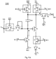
- FIG. 8A to Fig. 8C are schematic diagrams of the pixel circuit illustrated in Fig. 2 during various operation phases.
- the operation flow of the driving method of the pixel circuit provided by the embodiments of the present disclosure is described in detail below with reference to Fig. 2 , Fig. 7 and Fig. 8A to Fig. 8C .
- dotted line frames placed at positions of the transistors indicates that the transistors are in turn-off states, and no symbols placed at positions of transistors indicates that the transistors are in turn-on states.
- Solid lines with arrows indicate flow directions of signals.
- the first control signal S 1 provided by the first control terminal SC1 is a low level signal, so that the first bias transistor T4 and the second bias transistor T8 are turned on.
- the second control signal S 2 provided by the second control terminal SC2 is a high level signal
- the third control signal S 3 (i.e., the light emitting control signal) provided by the third control terminal SC3 is a high level signal, so that the data write transistor T2, the voltage drop compensation transistor T6, the first control transistor T7 and the second control transistor T5 are all in turn-off states.
- the first bias voltage terminal VB1 outputs the first bias voltage signal V init1 , and the first bias voltage signal V init1 is smaller than the sum of the threshold voltage V th2 of the threshold compensation transistor T3 and the data signal V data , so that the threshold compensation transistor T3 is in a turn-on state.
- the first bias voltage signal V init1 is transmitted to the gate electrode of the drive transistor T1 through the first bias transistor T4, so that the voltage of the gate electrode of the drive transistor T1 is reset to the first bias voltage signal V init1 .
- the second bias voltage terminal VB2 (i.e., the reset voltage terminal VR) can output the second bias voltage signal V init2 , and the second bias voltage signal V init2 is transmitted to the first electrode of the drive transistor T1 through the second bias transistor T8, so that the voltage of the first electrode of the drive transistor T1 is reset to the second bias voltage signal V init2 .
- the drive transistor T1 can be in a turn-on state.
- the drive transistor T1 is in a turn-on state.
- the present disclosure is not limited thereto, and during the reset phase RT, the drive transistor T1 can also be in a turn-off state.
- the first bias voltage signal V init1 and the second bias voltage signal V init2 can be same, in this situation, the drive transistor T1 is in a turn-off state.
- the first control signal S 1 is changed to a high level signal
- the second control signal S 2 is changed to a low level signal
- the third control signal S 3 maintains a high level signal.
- the first bias transistor T4, the second bias transistor T8, the first control transistor T7 and the second control transistor T5 are all in turn-off states
- the drive transistor T1, the data write transistor T2, the voltage drop compensation transistor T6 and the threshold compensation transistor T3 are all turned on.
- V data charges the second terminal of the storage capacitor Cst through the data write transistor T2 and the threshold compensation transistor T3 until the voltage of the second terminal of the storage capacitor Cst is V data +V th2 .
- Vt h2 is the threshold voltage of the threshold compensation transistor T3
- the threshold voltage Vt h2 of the threshold compensation transistor T3 is the same as the threshold voltage V th1 of the drive transistor T1, that is, the voltage of the second terminal of the storage capacitor Cst can be V data +V th1 .
- the voltage of the gate electrode of the drive transistor T1 is changed to V data +V th1 .
- the reference voltage signal V ref charges the first terminal of the storage capacitor Cst through the voltage drop compensation transistor T6, that is, the voltage of the first terminal of the storage capacitor Cst can be the reference voltage signal V ref , and in this situation, the voltage of the first electrode of the drive transistor T1 is changed to V ref .
- the first control signal S 1 maintains a high level signal
- the second control signal S 2 is changed to a high level signal
- the third control signal S 3 is changed to a low level signal.
- the first bias transistor T4, the second bias transistor T8, the data write transistor T2, the voltage drop compensation transistor T6 and the threshold compensation transistor T3 are all in turn-off states, and the drive transistor T1, the first control transistor T7 and the second control transistor T5 are all turned on.
- the first power voltage signal V dd output by the first power voltage terminal V1 can be transmitted to the first electrode of the drive transistor T1 through the second control transistor T5, and the voltage of the first electrode of the drive transistor T1 is changed to the first power voltage signal V dd . Because of the bootstrap effect of the storage capacitor Cst, the voltage of the gate electrode of the drive transistor T1 is changed to V data +V th1 +V dd -V ref .
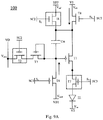
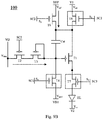
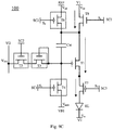
- FIG. 9A to Fig. 9C are schematic diagrams of the pixel circuit illustrated in Fig. 3 during various operation phases.
- the operation flow of driving method of another pixel circuit provided by the embodiments of the present disclosure is described in detail below with reference to Fig. 3 , Fig. 7 and Fig. 9A to Fig. 9C .
- dotted line frames placed at positions of the transistors indicates that the transistors are in turn-off states, and no symbols placed at positions of the transistors indicates that the transistors are in turn-on states.
- Solid lines with arrows indicate flow directions of signals.
- the first control signal S 1 provided by the first control terminal SC1 is a low level signal, so that the first bias transistor T4 is turned on.
- the second control signal S 2 provided by the second control terminal SC2 is a high level signal, so that the second bias transistor T8 is turned on, and the data write transistor T2 and the voltage drop compensation transistor T6 are in turn-off states.
- the third control signal S 3 (i.e., the light emitting control signal) provided by the third control terminal SC3 is a high level signal, so that the first control transistor T7 is in a turn-off state.
- the first bias voltage terminal VB1 outputs the first bias voltage signal V init1 , and the first bias voltage signal V init1 is smaller than the sum of the threshold voltage Vt h2 of the threshold compensation transistor T3 and the data signal V data , so that the threshold compensation transistor T3 is in a turn-on state.
- the first bias voltage signal V init1 is transmitted to the gate electrode of the drive transistor T1 through the first bias transistor T4, so that the voltage of the gate electrode of the drive transistor T1 is reset to the first bias voltage signal V init1 .
- the first power voltage terminal V1 (i.e., the second bias voltage terminal VB2) can output the first power voltage signal V dd , and the first power voltage signal V dd is transmitted to the first electrode of the drive transistor T1 through the second bias transistor T8, so that the voltage of the first electrode of the drive transistor T1 is reset to the first power voltage signal V dd .
- the drive transistor T1 can be in a turn-on state.
- the first power voltage signal V dd can be greater than the first bias voltage signal V init1 , and the difference between the first bias voltage signal V init1 and the first power voltage signal V dd is not larger than Vgs255 (the voltage difference between the gate electrode and the source electrode of the drive transistor T1 corresponding to the maximum gray scale), that is, V init1 -V dd is less than or equal to Vgs255.
- the drive transistor T1 is in a turn-on state.
- the present disclosure is not limited thereto, and during the reset phase RT, the drive transistor T1 can also be in a turn-off state.
- V init1 -V dd is larger than the threshold voltage V th1 of the drive transistor T1, in this situation, the drive transistor T1 is in a turn-off state.
- the first control signal S 1 is changed to a high level signal
- the second control signal S 2 is changed to a low level signal
- the third control signal S 3 maintains a high level signal.
- the first bias transistor T4, the second bias transistor T8 and the first control transistor T7 are all in turn-off states, and the drive transistor T1, the data write transistor T2, the voltage drop compensation transistor T6 and the threshold compensation transistor T3 are all turned on.
- V data charges the second terminal of the storage capacitor Cst through the data write transistor T2 and the threshold compensation transistor T3 until the voltage of the second terminal of the storage capacitor Cst is V data +V th2 .
- Vt h2 is the threshold voltage of the threshold compensation transistor T3
- the threshold voltage Vt h2 of the threshold compensation transistor T3 is the same as the threshold voltage V th1 of the drive transistor T1, that is, the voltage of the second terminal of the storage capacitor Cst can be V data +V th1 .
- the voltage of the gate electrode of the drive transistor T1 is changed to V data +V th1 .
- the reference voltage signal V ref charges the first terminal of the storage capacitor Cst through the voltage drop compensation transistor T6, that is, the voltage of the first terminal of the storage capacitor Cst can be the reference voltage signal V ref , and in this situation, the voltage of the first electrode of the drive transistor T1 is changed to V ref .
- the first control signal S 1 maintains a high level signal
- the second control signal S 2 is changed to a high level signal
- the third control signal S 3 is changed to a low level signal.
- the first bias transistor T4, the data write transistor T2, the voltage drop compensation transistor T6 and the threshold compensation transistor T3 are all in turn-off states, and the drive transistor T1, the first control transistor T7 and the second bias transistor T8 are all turned on.
- the first power voltage signal V dd output by the first power voltage terminal V1 can be transmitted to the first electrode of the drive transistor T1 through the second bias transistor T8, and the voltage of the first electrode of the drive transistor T1 is changed to the first power voltage signal V dd . Because of the bootstrap effect of the storage capacitor Cst, the voltage of the gate electrode of the drive transistor T1 is changed to V data +V th1 +V dd -V ref .
- V GS is the voltage difference between the gate electrode of the drive transistor T1 and the source electrode of the drive transistor T1
- V dd is the first power voltage signal output by the first power voltage terminal V1
- V th1 is the threshold voltage of the drive transistor T1. It can be seen from the above formula that the light emitting current I OLED is not affected by the threshold voltage V th1 of the drive transistor T1 and the first power voltage signal of the first power voltage terminal VI, but only related to the reference voltage signal V ref output by the reference power terminal REF and the data signal V data .
- the data signal V data is directly transmitted by the data signal terminal VD, and V data is independent of the threshold voltage V th of the drive transistor T1, so that the problem of the threshold voltage drift of the drive transistor T1 caused by the manufacture process and long-time operation can be solved.
- the reference voltage signal V ref is provided by the reference power terminal REF, which is independent of the IR drop of the first power voltage terminal VI, so that the problem of the IR drop of the display panel can be solved.
- the pixel circuit can ensure the accuracy of the light emitting current I OLED , eliminate the influence of the threshold voltage of the drive transistor T1 and the IR drop on the light emitting current I OLED , ensure the normal operation of the light emitting component EL, improve the uniformity of the display images, and improve the display effect.
- K 0.5 ⁇ n C ox W / L
- ⁇ n is the electron mobility of the drive transistor T1
- C ox is the unit capacitance of the gate electrode of the drive transistor T1
- W is the channel width of the drive transistor T1
- L is the channel length of the drive transistor T1.
- the driving method of the pixel circuit provided by the embodiments of the present disclosure allows the drive transistor to be in the bias state during the reset phase, so as to ameliorate the short-term afterimage problem caused by the hysteresis effect, and improve the display uniformity and display quality.
- the driving method of the pixel circuit provided by the embodiments of the present disclosure can also perform the threshold compensation operation and the voltage drop compensation operation, thereby compensating the threshold voltage drift of the drive transistor and the IR drop of the display panel, effectively improving the display effect of the display panel, and improving the display quality.
Landscapes
- Engineering & Computer Science (AREA)
- Physics & Mathematics (AREA)
- Computer Hardware Design (AREA)
- General Physics & Mathematics (AREA)
- Theoretical Computer Science (AREA)
- Control Of Indicators Other Than Cathode Ray Tubes (AREA)
- Control Of El Displays (AREA)
- Electroluminescent Light Sources (AREA)
Applications Claiming Priority (2)
| Application Number | Priority Date | Filing Date | Title |
|---|---|---|---|
| CN201711278159.XA CN109887464B (zh) | 2017-12-06 | 2017-12-06 | 像素电路及其驱动方法、显示面板和显示设备 |
| PCT/CN2018/102261 WO2019109673A1 (fr) | 2017-12-06 | 2018-08-24 | Circuit de pixel et son procédé d'attaque, panneau d'affichage et dispositif d'affichage |
Publications (2)
| Publication Number | Publication Date |
|---|---|
| EP3723075A1 true EP3723075A1 (fr) | 2020-10-14 |
| EP3723075A4 EP3723075A4 (fr) | 2021-08-18 |
Family
ID=66751298
Family Applications (1)
| Application Number | Title | Priority Date | Filing Date |
|---|---|---|---|
| EP18847206.2A Pending EP3723075A4 (fr) | 2017-12-06 | 2018-08-24 | Circuit de pixel et son procédé d'attaque, panneau d'affichage et dispositif d'affichage |
Country Status (4)
| Country | Link |
|---|---|
| US (1) | US11341908B2 (fr) |
| EP (1) | EP3723075A4 (fr) |
| CN (1) | CN109887464B (fr) |
| WO (1) | WO2019109673A1 (fr) |
Families Citing this family (23)
| Publication number | Priority date | Publication date | Assignee | Title |
|---|---|---|---|---|
| CN110197638A (zh) * | 2019-06-28 | 2019-09-03 | 上海天马有机发光显示技术有限公司 | 一种显示面板、显示装置和显示面板的驱动方法 |
| TWI697884B (zh) | 2019-08-20 | 2020-07-01 | 友達光電股份有限公司 | 畫素電路 |
| CN110675829B (zh) * | 2019-11-08 | 2021-03-12 | 京东方科技集团股份有限公司 | 像素驱动电路及其驱动方法、显示面板、显示装置 |
| KR102681836B1 (ko) * | 2020-03-03 | 2024-07-04 | 삼성디스플레이 주식회사 | 표시장치 |
| KR102662925B1 (ko) * | 2020-05-20 | 2024-05-08 | 삼성디스플레이 주식회사 | 화소 회로 및 이를 포함하는 표시 장치 |
| CN111883064B (zh) * | 2020-08-12 | 2022-04-22 | 合肥京东方显示技术有限公司 | 像素驱动电路及其驱动方法、显示面板与显示装置 |
| KR102726044B1 (ko) | 2020-09-25 | 2024-11-05 | 엘지디스플레이 주식회사 | 구동 회로와 이를 이용한 표시장치 |
| CN117238235A (zh) * | 2020-10-15 | 2023-12-15 | 厦门天马微电子有限公司 | 显示面板及其驱动方法以及显示装置 |
| CN112150967B (zh) * | 2020-10-20 | 2024-03-01 | 厦门天马微电子有限公司 | 一种显示面板、驱动方法及显示装置 |
| KR102951663B1 (ko) * | 2021-02-19 | 2026-04-14 | 삼성디스플레이 주식회사 | 표시 장치 |
| CN113421511B (zh) * | 2021-06-17 | 2022-05-03 | 昆山国显光电有限公司 | 显示面板的驱动方法、驱动装置及显示装置 |
| CN113327555B (zh) * | 2021-06-25 | 2023-04-18 | 合肥京东方卓印科技有限公司 | 像素电路、显示面板和控制方法 |
| WO2023004817A1 (fr) | 2021-07-30 | 2023-02-02 | 京东方科技集团股份有限公司 | Circuit d'attaque de pixel et procédé d'attaque associé, et panneau d'affichage |
| EP4300474A4 (fr) | 2021-07-30 | 2024-02-28 | BOE Technology Group Co., Ltd. | Circuit de pixels, procédé d'attaque et appareil d'affichage |
| CN114093299B (zh) * | 2022-01-24 | 2022-04-19 | 北京京东方技术开发有限公司 | 显示面板和显示装置 |
| CN114582289B (zh) * | 2022-04-21 | 2023-07-28 | 武汉天马微电子有限公司 | 显示面板及其驱动方法、显示装置 |
| US12223907B2 (en) | 2022-04-21 | 2025-02-11 | Chengdu Boe Optoelectronics Technology Co., Ltd. | Pixel circuit including a compensation control circuit, pixel driving method and display device |
| CN115188309B (zh) | 2022-06-29 | 2024-08-27 | 武汉天马微电子有限公司 | 显示面板及显示装置 |
| CN115691429B (zh) * | 2022-09-09 | 2025-04-29 | 厦门天马显示科技有限公司 | 一种显示面板及其驱动方法 |
| CN119296482A (zh) * | 2022-11-21 | 2025-01-10 | 武汉天马微电子有限公司 | 显示面板及其驱动方法、显示装置 |
| CN115909967A (zh) * | 2022-11-21 | 2023-04-04 | 合肥维信诺科技有限公司 | 像素电路及其驱动方法和显示面板 |
| WO2024152289A1 (fr) * | 2023-01-19 | 2024-07-25 | Boe Technology Group Co., Ltd. | Circuit d'attaque de pixels et appareil d'affichage |
| CN118262667A (zh) * | 2024-04-24 | 2024-06-28 | 合肥京东方卓印科技有限公司 | 像素电路、驱动方法和显示装置 |
Family Cites Families (9)
| Publication number | Priority date | Publication date | Assignee | Title |
|---|---|---|---|---|
| TWI559064B (zh) * | 2012-10-19 | 2016-11-21 | 日本顯示器股份有限公司 | Display device |
| KR20160038150A (ko) * | 2014-09-29 | 2016-04-07 | 삼성디스플레이 주식회사 | 표시장치 |
| KR102380303B1 (ko) * | 2014-12-18 | 2022-03-30 | 삼성디스플레이 주식회사 | 유기 발광 표시 장치 및 이의 구동 방법 |
| CN105096831B (zh) | 2015-08-21 | 2018-03-27 | 京东方科技集团股份有限公司 | 像素驱动电路、方法、显示面板和显示装置 |
| CN105845081A (zh) * | 2016-06-12 | 2016-08-10 | 京东方科技集团股份有限公司 | 像素电路、显示面板及驱动方法 |
| CN106940983A (zh) | 2017-05-11 | 2017-07-11 | 京东方科技集团股份有限公司 | 像素电路及其驱动方法、显示装置 |
| CN107331345A (zh) * | 2017-07-25 | 2017-11-07 | 武汉华星光电半导体显示技术有限公司 | 一种像素补偿电路及显示装置 |
| CN107358918B (zh) * | 2017-08-25 | 2023-11-21 | 京东方科技集团股份有限公司 | 一种像素电路及其驱动方法、显示装置 |
| CN107863072A (zh) | 2017-12-14 | 2018-03-30 | 京东方科技集团股份有限公司 | 显示装置、阵列基板、像素电路及其驱动方法 |
-
2017
- 2017-12-06 CN CN201711278159.XA patent/CN109887464B/zh active Active
-
2018
- 2018-08-24 EP EP18847206.2A patent/EP3723075A4/fr active Pending
- 2018-08-24 WO PCT/CN2018/102261 patent/WO2019109673A1/fr not_active Ceased
- 2018-08-24 US US16/327,653 patent/US11341908B2/en active Active
Also Published As
| Publication number | Publication date |
|---|---|
| CN109887464A (zh) | 2019-06-14 |
| EP3723075A4 (fr) | 2021-08-18 |
| WO2019109673A1 (fr) | 2019-06-13 |
| US20210327344A1 (en) | 2021-10-21 |
| US11341908B2 (en) | 2022-05-24 |
| CN109887464B (zh) | 2021-09-21 |
Similar Documents
| Publication | Publication Date | Title |
|---|---|---|
| US11341908B2 (en) | Pixel circuit and driving method thereof, display panel and display device | |
| US12573341B2 (en) | Pixel circuit and driving method thereof, and display panel | |
| US11393396B2 (en) | Pixel circuit and driving method therefor and display panel | |
| US11189228B2 (en) | Pixel circuit, method for driving pixel circuit, and display device | |
| US11217162B2 (en) | Pixel driving circuit, pixel circuit, display panel and display apparatus | |
| US11335269B2 (en) | Pixel circuit, display substrate and display apparatus | |
| US11270638B2 (en) | Display compensation circuit and method for controlling the same, and display apparatus | |
| KR101581147B1 (ko) | 외부 보상용 감지 회로, 이의 감지 방법 및 표시 장치 | |
| US9734763B2 (en) | Pixel circuit, driving method and display apparatus | |
| EP3739567A1 (fr) | Circuit de pixels, procédé de commande associé et panneau d'affichage | |
| US10515590B2 (en) | Pixel compensation circuit, driving method, display panel and display device | |
| US9972249B2 (en) | Pixel structure and driving method thereof, organic light emitting display panel and display apparatus | |
| US11029774B2 (en) | Touch panel in which cathodes serve as touch sense electrodes and a touch screen formed using the touch panel | |
| US20190325826A1 (en) | Pixel circuit, method for driving the same, display panel and display device | |
| US11355060B2 (en) | Pixel circuit, method of driving pixel circuit, display panel and display device | |
| US11568815B2 (en) | Pixel driving circuit, manufacturing method thereof, and display device | |
| CN111243543B (zh) | Goa电路、tft基板、显示装置及电子设备 | |
| US20160300531A1 (en) | Pixel circuit and display apparatus | |
| US10140922B2 (en) | Pixel driving circuit and driving method thereof and display device | |
| US12462757B2 (en) | Pixel driving circuit and driving method thereof, and display panel | |
| US11900883B2 (en) | Shift register unit, method for driving shift register unit, gate driving circuit, and display device | |
| US20210383753A1 (en) | Pixel Drive Circuit and Drive Method Thereof, and Display Device | |
| CN204117568U (zh) | 像素电路和显示装置 | |
| US11024232B2 (en) | Pixel driving circuit and driving method therefor, and display panel | |
| US10037730B2 (en) | Pixel circuit, drive method, array substrate, display panel and display device |
Legal Events
| Date | Code | Title | Description |
|---|---|---|---|
| STAA | Information on the status of an ep patent application or granted ep patent |
Free format text: STATUS: UNKNOWN |
|
| STAA | Information on the status of an ep patent application or granted ep patent |
Free format text: STATUS: THE INTERNATIONAL PUBLICATION HAS BEEN MADE |
|
| PUAI | Public reference made under article 153(3) epc to a published international application that has entered the european phase |
Free format text: ORIGINAL CODE: 0009012 |
|
| STAA | Information on the status of an ep patent application or granted ep patent |
Free format text: STATUS: REQUEST FOR EXAMINATION WAS MADE |
|
| 17P | Request for examination filed |
Effective date: 20190227 |
|
| AK | Designated contracting states |
Kind code of ref document: A1 Designated state(s): AL AT BE BG CH CY CZ DE DK EE ES FI FR GB GR HR HU IE IS IT LI LT LU LV MC MK MT NL NO PL PT RO RS SE SI SK SM TR |
|
| AX | Request for extension of the european patent |
Extension state: BA ME |
|
| DAV | Request for validation of the european patent (deleted) | ||
| DAX | Request for extension of the european patent (deleted) | ||
| A4 | Supplementary search report drawn up and despatched |
Effective date: 20210715 |
|
| RIC1 | Information provided on ipc code assigned before grant |
Ipc: G09G 3/3208 20160101AFI20210709BHEP Ipc: G09G 3/3233 20160101ALI20210709BHEP Ipc: G09G 3/3266 20160101ALI20210709BHEP Ipc: G09G 3/3291 20160101ALI20210709BHEP |
|
| STAA | Information on the status of an ep patent application or granted ep patent |
Free format text: STATUS: EXAMINATION IS IN PROGRESS |
|
| 17Q | First examination report despatched |
Effective date: 20230519 |