EP3723092A2 - Cellule de mémoire et réseau de cellules de mémoire à accès aléatoire magnétorésistive commandée par tension négative - Google Patents
Cellule de mémoire et réseau de cellules de mémoire à accès aléatoire magnétorésistive commandée par tension négative Download PDFInfo
- Publication number
- EP3723092A2 EP3723092A2 EP20164880.5A EP20164880A EP3723092A2 EP 3723092 A2 EP3723092 A2 EP 3723092A2 EP 20164880 A EP20164880 A EP 20164880A EP 3723092 A2 EP3723092 A2 EP 3723092A2
- Authority
- EP
- European Patent Office
- Prior art keywords
- voltage
- memory cell
- terminal
- pmos transistor
- storage element
- Prior art date
- Legal status (The legal status is an assumption and is not a legal conclusion. Google has not performed a legal analysis and makes no representation as to the accuracy of the status listed.)
- Ceased
Links
- 238000002955 isolation Methods 0.000 claims description 6
- 230000003247 decreasing effect Effects 0.000 claims description 3
- 238000010586 diagram Methods 0.000 description 4
- 230000005415 magnetization Effects 0.000 description 4
- 238000012986 modification Methods 0.000 description 3
- 230000004048 modification Effects 0.000 description 3
- 230000000694 effects Effects 0.000 description 2
- 238000000034 method Methods 0.000 description 2
- 230000004075 alteration Effects 0.000 description 1
- 238000007796 conventional method Methods 0.000 description 1
- 230000007850 degeneration Effects 0.000 description 1
- 239000013642 negative control Substances 0.000 description 1
Images
Classifications
-
- G—PHYSICS
- G11—INFORMATION STORAGE
- G11C—STATIC STORES
- G11C11/00—Digital stores characterised by the use of particular electric or magnetic storage elements; Storage elements therefor
- G11C11/02—Digital stores characterised by the use of particular electric or magnetic storage elements; Storage elements therefor using magnetic elements
- G11C11/16—Digital stores characterised by the use of particular electric or magnetic storage elements; Storage elements therefor using magnetic elements using elements in which the storage effect is based on magnetic spin effect
- G11C11/161—Digital stores characterised by the use of particular electric or magnetic storage elements; Storage elements therefor using magnetic elements using elements in which the storage effect is based on magnetic spin effect details concerning the memory cell structure, e.g. the layers of the ferromagnetic memory cell
-
- G—PHYSICS
- G11—INFORMATION STORAGE
- G11C—STATIC STORES
- G11C11/00—Digital stores characterised by the use of particular electric or magnetic storage elements; Storage elements therefor
- G11C11/02—Digital stores characterised by the use of particular electric or magnetic storage elements; Storage elements therefor using magnetic elements
- G11C11/16—Digital stores characterised by the use of particular electric or magnetic storage elements; Storage elements therefor using magnetic elements using elements in which the storage effect is based on magnetic spin effect
- G11C11/165—Auxiliary circuits
- G11C11/1659—Cell access
-
- H—ELECTRICITY
- H03—ELECTRONIC CIRCUITRY
- H03K—PULSE TECHNIQUE
- H03K19/00—Logic circuits, i.e. having at least two inputs acting on one output; Inverting circuits
- H03K19/0008—Arrangements for reducing power consumption
- H03K19/0013—Arrangements for reducing power consumption in field effect transistor circuits
-
- G—PHYSICS
- G11—INFORMATION STORAGE
- G11C—STATIC STORES
- G11C11/00—Digital stores characterised by the use of particular electric or magnetic storage elements; Storage elements therefor
- G11C11/02—Digital stores characterised by the use of particular electric or magnetic storage elements; Storage elements therefor using magnetic elements
- G11C11/16—Digital stores characterised by the use of particular electric or magnetic storage elements; Storage elements therefor using magnetic elements using elements in which the storage effect is based on magnetic spin effect
- G11C11/165—Auxiliary circuits
-
- G—PHYSICS
- G11—INFORMATION STORAGE
- G11C—STATIC STORES
- G11C11/00—Digital stores characterised by the use of particular electric or magnetic storage elements; Storage elements therefor
- G11C11/02—Digital stores characterised by the use of particular electric or magnetic storage elements; Storage elements therefor using magnetic elements
- G11C11/16—Digital stores characterised by the use of particular electric or magnetic storage elements; Storage elements therefor using magnetic elements using elements in which the storage effect is based on magnetic spin effect
- G11C11/165—Auxiliary circuits
- G11C11/1673—Reading or sensing circuits or methods
-
- G—PHYSICS
- G11—INFORMATION STORAGE
- G11C—STATIC STORES
- G11C11/00—Digital stores characterised by the use of particular electric or magnetic storage elements; Storage elements therefor
- G11C11/02—Digital stores characterised by the use of particular electric or magnetic storage elements; Storage elements therefor using magnetic elements
- G11C11/16—Digital stores characterised by the use of particular electric or magnetic storage elements; Storage elements therefor using magnetic elements using elements in which the storage effect is based on magnetic spin effect
- G11C11/165—Auxiliary circuits
- G11C11/1675—Writing or programming circuits or methods
-
- G—PHYSICS
- G11—INFORMATION STORAGE
- G11C—STATIC STORES
- G11C11/00—Digital stores characterised by the use of particular electric or magnetic storage elements; Storage elements therefor
- G11C11/02—Digital stores characterised by the use of particular electric or magnetic storage elements; Storage elements therefor using magnetic elements
- G11C11/16—Digital stores characterised by the use of particular electric or magnetic storage elements; Storage elements therefor using magnetic elements using elements in which the storage effect is based on magnetic spin effect
- G11C11/165—Auxiliary circuits
- G11C11/1697—Power supply circuits
-
- G—PHYSICS
- G11—INFORMATION STORAGE
- G11C—STATIC STORES
- G11C16/00—Erasable programmable read-only memories
- G11C16/02—Erasable programmable read-only memories electrically programmable
- G11C16/06—Auxiliary circuits, e.g. for writing into memory
- G11C16/08—Address circuits; Decoders; Word-line control circuits
-
- G—PHYSICS
- G11—INFORMATION STORAGE
- G11C—STATIC STORES
- G11C16/00—Erasable programmable read-only memories
- G11C16/02—Erasable programmable read-only memories electrically programmable
- G11C16/06—Auxiliary circuits, e.g. for writing into memory
- G11C16/10—Programming or data input circuits
- G11C16/14—Circuits for erasing electrically, e.g. erase voltage switching circuits
-
- G—PHYSICS
- G11—INFORMATION STORAGE
- G11C—STATIC STORES
- G11C16/00—Erasable programmable read-only memories
- G11C16/02—Erasable programmable read-only memories electrically programmable
- G11C16/06—Auxiliary circuits, e.g. for writing into memory
- G11C16/10—Programming or data input circuits
- G11C16/14—Circuits for erasing electrically, e.g. erase voltage switching circuits
- G11C16/16—Circuits for erasing electrically, e.g. erase voltage switching circuits for erasing blocks, e.g. arrays, words, groups
-
- G—PHYSICS
- G11—INFORMATION STORAGE
- G11C—STATIC STORES
- G11C16/00—Erasable programmable read-only memories
- G11C16/02—Erasable programmable read-only memories electrically programmable
- G11C16/06—Auxiliary circuits, e.g. for writing into memory
- G11C16/24—Bit-line control circuits
-
- G—PHYSICS
- G11—INFORMATION STORAGE
- G11C—STATIC STORES
- G11C16/00—Erasable programmable read-only memories
- G11C16/02—Erasable programmable read-only memories electrically programmable
- G11C16/06—Auxiliary circuits, e.g. for writing into memory
- G11C16/26—Sensing or reading circuits; Data output circuits
-
- G—PHYSICS
- G11—INFORMATION STORAGE
- G11C—STATIC STORES
- G11C5/00—Details of stores covered by group G11C11/00
- G11C5/02—Disposition of storage elements, e.g. in the form of a matrix array
- G11C5/025—Geometric lay-out considerations of storage- and peripheral-blocks in a semiconductor storage device
-
- G—PHYSICS
- G11—INFORMATION STORAGE
- G11C—STATIC STORES
- G11C7/00—Arrangements for writing information into, or reading information out from, a digital store
- G11C7/06—Sense amplifiers; Associated circuits, e.g. timing or triggering circuits
-
- G—PHYSICS
- G11—INFORMATION STORAGE
- G11C—STATIC STORES
- G11C7/00—Arrangements for writing information into, or reading information out from, a digital store
- G11C7/10—Input/output [I/O] data interface arrangements, e.g. I/O data control circuits, I/O data buffers
- G11C7/1051—Data output circuits, e.g. read-out amplifiers, data output buffers, data output registers, data output level conversion circuits
-
- G—PHYSICS
- G11—INFORMATION STORAGE
- G11C—STATIC STORES
- G11C7/00—Arrangements for writing information into, or reading information out from, a digital store
- G11C7/10—Input/output [I/O] data interface arrangements, e.g. I/O data control circuits, I/O data buffers
- G11C7/1078—Data input circuits, e.g. write amplifiers, data input buffers, data input registers, data input level conversion circuits
- G11C7/1084—Data input buffers, e.g. comprising level conversion circuits, circuits for adapting load
-
- H—ELECTRICITY
- H03—ELECTRONIC CIRCUITRY
- H03K—PULSE TECHNIQUE
- H03K17/00—Electronic switching or gating, i.e. not by contact-making and –breaking
- H03K17/16—Modifications for eliminating interference voltages or currents
- H03K17/161—Modifications for eliminating interference voltages or currents in field-effect transistor switches
- H03K17/162—Modifications for eliminating interference voltages or currents in field-effect transistor switches without feedback from the output circuit to the control circuit
-
- H—ELECTRICITY
- H03—ELECTRONIC CIRCUITRY
- H03K—PULSE TECHNIQUE
- H03K17/00—Electronic switching or gating, i.e. not by contact-making and –breaking
- H03K17/51—Electronic switching or gating, i.e. not by contact-making and –breaking characterised by the components used
- H03K17/56—Electronic switching or gating, i.e. not by contact-making and –breaking characterised by the components used by the use, as active elements, of semiconductor devices
- H03K17/687—Electronic switching or gating, i.e. not by contact-making and –breaking characterised by the components used by the use, as active elements, of semiconductor devices the devices being field-effect transistors
- H03K17/6871—Electronic switching or gating, i.e. not by contact-making and –breaking characterised by the components used by the use, as active elements, of semiconductor devices the devices being field-effect transistors the output circuit comprising more than one controlled field-effect transistor
-
- H—ELECTRICITY
- H03—ELECTRONIC CIRCUITRY
- H03K—PULSE TECHNIQUE
- H03K19/00—Logic circuits, i.e. having at least two inputs acting on one output; Inverting circuits
- H03K19/0175—Coupling arrangements; Interface arrangements
- H03K19/0185—Coupling arrangements; Interface arrangements using field effect transistors only
- H03K19/018507—Interface arrangements
- H03K19/018521—Interface arrangements of complementary type, e.g. CMOS
- H03K19/018528—Interface arrangements of complementary type, e.g. CMOS with at least one differential stage
-
- H—ELECTRICITY
- H03—ELECTRONIC CIRCUITRY
- H03K—PULSE TECHNIQUE
- H03K19/00—Logic circuits, i.e. having at least two inputs acting on one output; Inverting circuits
- H03K19/02—Logic circuits, i.e. having at least two inputs acting on one output; Inverting circuits using specified components
- H03K19/08—Logic circuits, i.e. having at least two inputs acting on one output; Inverting circuits using specified components using semiconductor devices
- H03K19/094—Logic circuits, i.e. having at least two inputs acting on one output; Inverting circuits using specified components using semiconductor devices using field-effect transistors
- H03K19/0944—Logic circuits, i.e. having at least two inputs acting on one output; Inverting circuits using specified components using semiconductor devices using field-effect transistors using MOSFET or insulated gate field-effect transistors, i.e. IGFET
-
- H—ELECTRICITY
- H03—ELECTRONIC CIRCUITRY
- H03K—PULSE TECHNIQUE
- H03K3/00—Circuits for generating electric pulses; Monostable, bistable or multistable circuits
- H03K3/02—Generators characterised by the type of circuit or by the means used for producing pulses
- H03K3/353—Generators characterised by the type of circuit or by the means used for producing pulses by the use, as active elements, of field-effect transistors with internal or external positive feedback
- H03K3/356—Bistable circuits
-
- H—ELECTRICITY
- H10—SEMICONDUCTOR DEVICES; ELECTRIC SOLID-STATE DEVICES NOT OTHERWISE PROVIDED FOR
- H10B—ELECTRONIC MEMORY DEVICES
- H10B61/00—Magnetic memory devices, e.g. magnetoresistive RAM [MRAM] devices
- H10B61/20—Magnetic memory devices, e.g. magnetoresistive RAM [MRAM] devices comprising components having three or more electrodes, e.g. transistors
-
- G—PHYSICS
- G05—CONTROLLING; REGULATING
- G05F—SYSTEMS FOR REGULATING ELECTRIC OR MAGNETIC VARIABLES
- G05F3/00—Non-retroactive systems for regulating electric variables by using an uncontrolled element, or an uncontrolled combination of elements, such element or such combination having self-regulating properties
- G05F3/02—Regulating voltage or current
- G05F3/08—Regulating voltage or current wherein the variable is DC
- G05F3/10—Regulating voltage or current wherein the variable is DC using uncontrolled devices with non-linear characteristics
- G05F3/16—Regulating voltage or current wherein the variable is DC using uncontrolled devices with non-linear characteristics being semiconductor devices
- G05F3/20—Regulating voltage or current wherein the variable is DC using uncontrolled devices with non-linear characteristics being semiconductor devices using diode- transistor combinations
- G05F3/26—Current mirrors
- G05F3/262—Current mirrors using field-effect transistors only
-
- G—PHYSICS
- G05—CONTROLLING; REGULATING
- G05F—SYSTEMS FOR REGULATING ELECTRIC OR MAGNETIC VARIABLES
- G05F3/00—Non-retroactive systems for regulating electric variables by using an uncontrolled element, or an uncontrolled combination of elements, such element or such combination having self-regulating properties
- G05F3/02—Regulating voltage or current
- G05F3/08—Regulating voltage or current wherein the variable is DC
- G05F3/10—Regulating voltage or current wherein the variable is DC using uncontrolled devices with non-linear characteristics
- G05F3/16—Regulating voltage or current wherein the variable is DC using uncontrolled devices with non-linear characteristics being semiconductor devices
- G05F3/20—Regulating voltage or current wherein the variable is DC using uncontrolled devices with non-linear characteristics being semiconductor devices using diode- transistor combinations
- G05F3/26—Current mirrors
- G05F3/267—Current mirrors using both bipolar and field-effect technology
-
- H—ELECTRICITY
- H02—GENERATION; CONVERSION OR DISTRIBUTION OF ELECTRIC POWER
- H02M—APPARATUS FOR CONVERSION BETWEEN AC AND AC, BETWEEN AC AND DC, OR BETWEEN DC AND DC, AND FOR USE WITH MAINS OR SIMILAR POWER SUPPLY SYSTEMS; CONVERSION OF DC OR AC INPUT POWER INTO SURGE OUTPUT POWER; CONTROL OR REGULATION THEREOF
- H02M3/00—Conversion of DC power input into DC power output
- H02M3/02—Conversion of DC power input into DC power output without intermediate conversion into AC
- H02M3/04—Conversion of DC power input into DC power output without intermediate conversion into AC by static converters
- H02M3/06—Conversion of DC power input into DC power output without intermediate conversion into AC by static converters using resistors or capacitors, e.g. potential divider
- H02M3/07—Conversion of DC power input into DC power output without intermediate conversion into AC by static converters using resistors or capacitors, e.g. potential divider using capacitors charged and discharged alternately by semiconductor devices with control electrode, e.g. charge pumps
-
- H—ELECTRICITY
- H03—ELECTRONIC CIRCUITRY
- H03K—PULSE TECHNIQUE
- H03K2217/00—Indexing scheme related to electronic switching or gating, i.e. not by contact-making or -breaking covered by H03K17/00
- H03K2217/0036—Means reducing energy consumption
Definitions
- the present invention relates to a non-volatile memory, and more particularly to a magnetoresistive random access memory (MRAM) that is operated by a negative voltage.
- MRAM magnetoresistive random access memory
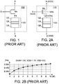
- FIG. 1 is a schematic circuit diagram illustrating a conventional MRAM cell.
- the conventional MRAM cell 110 comprises a switch transistor Ms and a storage element 120.
- the storage element 120 is a magnetic tunnel junction (MTJ).
- MTJ magnetic tunnel junction
- the MRAM cell 110 has three ends A, B and S.
- a first terminal of the switch transistor Ms is connected with the end A.
- a second terminal of the switch transistor Ms is connected with a node "a".
- a control terminal is connected with the end S.
- the switch transistor Ms is a NMOS transistor.
- the gate terminal of the switch transistor Ms is the control terminal.
- the storage element 120 comprises a pin layer 122, an isolation layer 124 and a free layer 126, which are arranged in a stack form.
- the pin layer 122 of the storage element 120 is connected with the node "a".
- the free layer 126 of the storage element 120 is connected with the end B.
- the storage element 120 has the higher impedance (e.g., 5.2 kohms). Meanwhile, the MRAM cell 110 is in a first storage state, which is also referred as a high impedance state. Whereas, in case that the magnetization directions of the pin layer 122 and the free layer 126 are identical the storage element 120 has the lower impedance (e.g., 3.2 kohms). Meanwhile, the MRAM cell 110 is in a second storage state, which is also referred as a low impedance state. Moreover, by applying the current and voltage in different direction, the MRAM cell 110 is controlled to be in the first storage state or the second storage state.
- the MRAM cell 110 is controlled to be in the first storage state or the second storage state.
- the MRAM cell 110 as shown in FIG. 1 has other configurations.
- the pin layer 122 of the storage element 120 is connected with the end B and the free layer 126 of the storage element 120 is connected with the node "a".
- FIG. 2A schematically illustrates associated bias voltages for performing a write operation on the conventional MRAM cell to program the conventional MRAM cell into a first storage state.
- a first voltage VDD is provided to the end A.
- a second voltage VSS is provided to the end B.
- the magnitude of the first voltage VDD is 1.1V
- the magnitude of the second voltage VSS is the ground voltage (0V).
- a control voltage Vctrl is provided to the end S to control the switch transistor Ms. Consequently, a current I is generated within the MRAM cell 110. The current I flows from the end A to the end B through the node "a". Consequently, the MRAM cell 110 is programmed to the first storage state.
- the MRAM cell 110 may be programmed into the second storage state through the write operation. That is, the first voltage VDD is provided to the end B, and the second voltage VSS is provided to the end A. When the switch transistor Ms is turned on, the current flows from the end B to the end A through the node "a". Consequently, the MRAM cell 110 is programmed to the second storage state.
- a first voltage difference received by the two terminals of the storage element 120 needs to be at least 0.55V. That is, when the voltage of the end B is the second voltage VSS (e.g., 0V) and the voltage Va at the node "a" is higher than 0.55V, the MRAM cell 110 is in the first storage state. Furthermore, for changing to the second storage state of the MRAM cell 110, a second voltage difference received by two terminals of the storage element 120 need to be at least 0.45V. That is, when the voltage of the end B is the first voltage VDD (e.g., 1.1V) and the voltage Va at the node "a" needs to be lower than 0.65V, the MRAM cell 110 is in the second storage state.
- the switch transistor Ms is a NMOS transistor. Consequently, the body terminal of the switch transistor Ms is connected with the lowest voltage (i.e., the second voltage VSS). Moreover, when the first voltage VDD is used as the control voltage Vctrl, the switch transistor Ms is turned on.
- the switch transistor Ms due to the voltage difference between the body terminal of the switch transistor Ms and the second terminal of the switch transistor Ms (i.e., the node "a"), the switch transistor Ms is possibly suffered from a serious body effect and a serious source degeneration problem. Under this circumstance, the resistance of the switch transistor Ms is very large. Moreover, during the write operation of the MRAM cell 110, the voltage Va at the node "a" cannot reach 0.55V. Under this circumstances, the MRAM cell 110 is almost impossible to be changed to the first storage state.
- the control voltage Vctrl applied to the end S needs to be increased and thus the voltage Va at the node "a" reaches 0.55V.
- the control voltage Vctrl applied to the end S is increased from the first voltage VDD (e.g., 1.1V) to 1.5V
- the size of the switch transistor Ms has to be increased after the control voltage Vctrl applied to the control terminal of the switch transistor Ms is increased. In other words, the array size of the MRAM cell 110 is also increased.
- FIG. 2B is a plot illustrating the relationship between the voltage Va of the node a and the size of the switch transistor Ms in the conventional MRAM cell.
- M the basic size of the switch transistor Ms
- M the size of the switch transistor Ms is twice the basic size. The rest may be deduced by analogy.
- the size of the switch transistor Ms is at least eight times the basic size and the control voltage Vctrl is 1.5V, the voltage Va at the node "a" reaches 0.55V and the storage element 120 of the MRAM cell 110 is controlled to be in the first storage state.
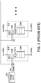
- FIG. 3 schematically illustrates associated bias voltages for performing a write operation on the conventional MRAM cell array.
- the MRAM cell array comprises plural MRAM cells in a row. For succinctness, only two MRAM cells 210 and 310 are shown.
- the MRAM cells 210 and 310 are connected with a word line WL.
- the MRAM cell 210 comprises a switch transistor Ms1 and a storage element 220.
- the MRAM cell 310 comprises a switch transistor Ms2 and a storage element 320.
- the structures of the MRAM cells 210 and 310 are similar to the structure of the MRAM cell 110 as shown in FIG. 1 , and are not redundantly described herein.
- the end S1 of the MRAM cell 210 and the end S2 of the MRAM cell 310 are connected with the word line WL.
- the word line WL is connected with a charge pump 330.
- the charge pump 330 provides the control voltage Vctrl.
- the charge pump 330 can increase the magnitude of the first voltage VDD (e.g., 1.1V) to the magnitude of the control voltage Vctrl (e.g., 1.5V).
- the MRAM cell 210 and the MRAM cell 310 are respectively programmed to the first storage state and the second storage state through the write operation.
- the other MRAM cells in the same row may be programmed to the first storage state or the second storage state according to the similar method.
- the end A1 of the MRAM cell 210 receives the first voltage VDD.
- the end B1 of the MRAM cell 210 receives the second voltage VSS.
- the end A2 of the MRAM cell 310 receives the second voltage VSS.
- the end B2 of the MRAM cell 310 receives the first voltage VDD.
- the word line WL receives the control voltage Vctrl and the switch transistors Ms1 and Ms2 are turned on, the current I1 generated within the MRAM cell 210 flows from the end A1 to the end B1 through the node a1 and the current I2 generated within the MRAM cell 310 flows from the end B2 to the end A2 through the node a2. Consequently, the MRAM cell 210 is in the first storage state, and the MRAM cell 310 is in the second storage state.
- the control voltage Vctrl is1.5V, and the end A2 receives the second voltage VSS (0V). Consequently, the voltage difference between the gate terminal and the source terminal of the switch transistor Ms2 is very high, the switch transistor Ms2 cannot comply with the safe operation area (SOA) criteria. Under this circumstance, the switch transistor Ms2 is damaged.
- SOA safe operation area
- the voltage received by the end A2 has to be increased from the second voltage VSS (0V) to a third voltage (e.g., 0.4V). Consequently, the voltage difference between the gate terminal and the source terminal of the switch transistor Ms2 can comply with the SOA criteria.
- the control voltage Vctrl e.g., 1.5V
- the first voltage VDD e.g., 1.1V
- the second voltage VSS e.g., 0V
- the third voltage e.g., 0.4V
- An embodiment of the present invention provides a memory cell of a magnetoresistive random access memory.
- the memory cell includes a PMOS transistor and a storage element.
- a first terminal of the PMOS transistor is connected with a first end of the memory cell.
- a control terminal of the PMOS transistor is connected with a second end of the memory cell.
- a first terminal of the storage element is connected with a second terminal of the PMOS transistor.
- a second terminal of the storage element is connected with a third end of the memory cell.
- the memory cell array includes a first memory cell and a second memory cell.
- the first memory cell includes a first PMOS transistor and a first storage element.
- the second memory cell includes a second PMOS transistor and a second storage element.
- a first terminal of the first PMOS transistor is connected with a first end of the first memory cell.
- a control terminal of the first PMOS transistor is connected with a word line.
- a first terminal of the first storage element is connected with a second terminal of the first PMOS transistor.
- a second terminal of the first storage element is connected with a second end of the first memory cell.
- a first terminal of the second PMOS transistor is connected with a first end of the second memory cell.
- a control terminal of the second PMOS transistor is connected with the word line.
- a first terminal of the second storage element is connected with a second terminal of the second PMOS transistor.
- a second terminal of the second storage element is connected with a second end of the second memory cell. While a write operation is performed, a control voltage is provided to the word line, a first voltage difference is provided to two terminals of the first storage element, a second voltage difference is provided to two terminals of the second storage element. Consequently, the first memory cell is in a first storage state and the second memory cell is in a second storage state.
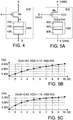
- FIG. 4 is a schematic circuit diagram illustrating a MRAM cell according to an embodiment of the present invention.
- the MRAM cell 410 comprises a switch transistor Ms and a storage element 420.
- the MRAM cell 410 has three ends A, B and S.
- a first terminal of the switch transistor Ms is connected with the end A.
- a second terminal of the switch transistor Ms is connected with a node "a".
- a control terminal is connected with the end S.
- the switch transistor Ms is a PMOS transistor.
- the gate terminal of the switch transistor Ms is the control terminal.
- the storage element 420 comprises a pin layer 422, an isolation layer 424 and a free layer 426, which are arranged in a stack form.
- the pin layer 422 of the storage element 420 is connected with the node "a".
- the free layer 426 of the storage element 420 is connected with the end B.
- the storage element 420 has the higher impedance (e.g., 5.2 kohms). Meanwhile, the MRAM cell 410 is in a first storage state, which is also referred as a high impedance state. Whereas, in case that the magnetization directions of the pin layer 422 and the free layer 426 are identical the storage element 420 has the lower impedance (e.g., 3.2 kohms). Meanwhile, the MRAM cell 410 is in a second storage state, which is also referred as a low impedance state. Moreover, by applying the current and voltage in different direction, the MRAM cell 410 is controlled to be in the first storage state or the second storage state.
- the MRAM cell 410 is controlled to be in the first storage state or the second storage state.
- the MRAM cell 410 of the present invention has other configurations.
- the pin layer 422 of the storage element 420 is connected with the end B and the free layer 426 of the storage element 420 is connected with the node "a".
- FIG. 5A schematically illustrates associated bias voltages for performing a write operation on the MRAM cell to program the MRAM cell into a first storage state.
- a first voltage VDD is provided to the end A.
- a second voltage VSS is provided to the end B.
- the magnitude of the first voltage VDD is 1.1V
- the magnitude of the second voltage VSS is the ground voltage (0V).
- the switch transistor Ms is a PMOS transistor. Consequently, the body terminal of the switch transistor Ms is connected with the highest voltage (i.e., the first voltage VDD).
- a control voltage Vctrl is provided to the end S to control the switch transistor Ms. Consequently, a current I is generated within the MRAM cell 410. The current I flows from the end A to the end B through the node "a". Consequently, the MRAM cell 410 is programmed to the first storage state.
- the MRAM cell 410 may be programmed into the second storage state through the write operation. That is, the first voltage VDD is provided to the end B, and the second voltage VSS is provided to the end A. When the switch transistor Ms is turned on, the current flows from the end B to the end A through the node "a". Consequently, the MRAM cell 410 is programmed to the second storage state.
- the first voltage difference received by the two terminals of the storage element 420 needs to be higher than 0.55V. That is, when the voltage of the end B is the second voltage VSS (e.g., 0V) and the voltage Va at the node "a" is higher than 0.55V, the MRAM cell 410 is in the first storage state. Furthermore, for changing to the second storage state of the MRAM cell 410, the second voltage difference received by two terminals of the storage element 420 need to be at least 0.45V. That is, when the voltage of the end B is the first voltage VDD (e.g., 1.1V) and the voltage Va at the node "a" is lower than 0.65V, the MRAM cell 410 is in the second storage state.
- VDD e.g., 1.1V
- the body terminal of the switch transistor Ms and the first terminal of the switch transistor Ms are connected with the first voltage VDD, the switch transistor Ms is not suffered from the serious body effect. Consequently, during the write operation of the MRAM cell 410, the resistance of the switch transistor Ms is low.
- FIG. 5B is a plot illustrating the relationship between the voltage Va of the node a and the size of the switch transistor Ms in the MRAM cell of the present invention when the control voltage Vctrl is 0V
- the size of the switch transistor Ms is at least eight times the basic size and the control voltage Vctrl is 0V, the voltage Va at the node "a" reaches 0.55V and the MRAM cell 410 is controlled to be in the first storage state.
- FIG. 5C is a plot illustrating the relationship between the voltage Va of the node a and the size of the switch transistor Ms in the MRAM cell of the present invention when the control voltage Vctrl is -0.4V.
- the use of the smaller-size PMOS transistor as the switch transistor Ms and the provision of the negative control voltage Vctrl can effectively reduce the resistance of the switch transistor Ms and control the MRAM cell 410 to be in the first storage state successfully.
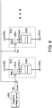
- FIG. 6 schematically illustrates associated bias voltages for performing a write operation on the MRAM cell array of the present invention.
- the MRAM cell array comprises plural MRAM cells in a row. For succinctness, only two MRAM cells 510 and 610 are shown.
- the MRAM cells 510 and 610 are connected with a word line WL.
- the MRAM cell 510 comprises a switch transistor Ms1 and a storage element 520.
- the MRAM cell 610 comprises a switch transistor Ms2 and a storage element 620.
- the structures of the MRAM cells 510 and 610 are similar to the structure of the MRAM cell 410 as shown in FIG. 4 , and are not redundantly described herein.
- the end S1 of the MRAM cell 510 and the end S2 of the MRAM cell 610 are connected with the word line WL.
- the word line WL is connected with a negative charge pump 630.
- the negative charge pump 630 provides the control voltage Vctrl with a negative voltage level.
- the negative charge pump 630 can decrease the magnitude of the second voltage VSS (e.g., 0V) to the magnitude of the control voltage Vctrl (e.g., -0.4V).
- the MRAM cell 510 and the MRAM cell 610 are respectively programmed to the first storage state and the second storage state through the write operation.
- the other MRAM cells in the same row may be programmed to the first storage state or the second storage state according to the similar method.
- the end A1 of the MRAM cell 510 receives the first voltage VDD.
- the end B1 of the MRAM cell 510 receives the second voltage VSS.
- the end A2 of the MRAM cell 610 receives the second voltage VSS.
- the end B2 of the MRAM cell 610 receives the first voltage VDD.
- the word line WL receives the control voltage Vctrl with the negative voltage level and the switch transistors Ms1 and Ms2 are turned on, the current I1 generated within the MRAM cell 510 flows from the end A1 to the end B1 through the node a1 and the current I2 generated within the MRAM cell 610 flows from the end B2 to the end A2 through the node a2. Consequently, the MRAM cell 510 is in the first storage state, and the MRAM cell 610 is in the second storage state.
- the body terminal of the switch transistor Ms is connected with the first voltage VDD. It is noted that numerous modifications and alterations may be made while retaining the teachings of the invention.
- the body terminal of the switch transistor is connected with another voltage (e.g., a fourth voltage) at a proper time. The magnitude of the fourth voltage is equal to the voltage Va at the node "a".
- the end A1 of the MRAM cell 510 receives a regulator voltage less than the first voltage VDD, if there is a need that the switch transistor Ms1 should comply with the safe operation area (SOA) criteria.
- SOA safe operation area
- the present invention provides a magnetoresistive random access memory (MRAM) that is operated by a negative voltage.
- the magnetoresistive random access memory comprises a MRAM cell array.
- the MRAM cell array is connected with a word line WL.
- the MRAM cell array comprises plural MRAM cells.
- Each MRAM cell comprises a switch transistor and a storage element.
- the switch transistor is a PMOS transistor.
- the control voltage with the negative voltage level is provided to the word line, and the first voltage VDD and the second voltage VSS are provided to the two ends A and B of the MRAM cell. Consequently, the MRAM cell is controlled to be in the first storage state or the second storage state.
- the magnitude of the first voltage VDD is higher than the magnitude of the second voltage VSS.
- the magnitude of the second voltage VSS is higher than the magnitude of the control voltage Vctrl. Since the size of the switch transistor of the MRAM cell is reduced, the storage density of the MRAM is effectively increased and the fabricating cost of the MRAM is effectively reduced.
Landscapes
- Engineering & Computer Science (AREA)
- Computer Hardware Design (AREA)
- Physics & Mathematics (AREA)
- Computing Systems (AREA)
- General Engineering & Computer Science (AREA)
- Mathematical Physics (AREA)
- Microelectronics & Electronic Packaging (AREA)
- Power Engineering (AREA)
- General Physics & Mathematics (AREA)
- Nonlinear Science (AREA)
- Radar, Positioning & Navigation (AREA)
- Automation & Control Theory (AREA)
- Electromagnetism (AREA)
- Read Only Memory (AREA)
- Electronic Switches (AREA)
- Mram Or Spin Memory Techniques (AREA)
- Control Of Electrical Variables (AREA)
- Dc-Dc Converters (AREA)
- Hall/Mr Elements (AREA)
- Amplifiers (AREA)
- Non-Volatile Memory (AREA)
- Static Random-Access Memory (AREA)
Applications Claiming Priority (1)
| Application Number | Priority Date | Filing Date | Title |
|---|---|---|---|
| US201962832853P | 2019-04-11 | 2019-04-11 |
Publications (2)
| Publication Number | Publication Date |
|---|---|
| EP3723092A2 true EP3723092A2 (fr) | 2020-10-14 |
| EP3723092A3 EP3723092A3 (fr) | 2020-12-16 |
Family
ID=69960257
Family Applications (1)
| Application Number | Title | Priority Date | Filing Date |
|---|---|---|---|
| EP20164880.5A Ceased EP3723092A3 (fr) | 2019-04-11 | 2020-03-23 | Cellule de mémoire magnétorésistive commandée par une tension négative |
Country Status (4)
| Country | Link |
|---|---|
| US (6) | US10924112B2 (fr) |
| EP (1) | EP3723092A3 (fr) |
| CN (6) | CN111813170B (fr) |
| TW (6) | TWI710876B (fr) |
Families Citing this family (6)
| Publication number | Priority date | Publication date | Assignee | Title |
|---|---|---|---|---|
| US10924112B2 (en) * | 2019-04-11 | 2021-02-16 | Ememory Technology Inc. | Bandgap reference circuit |
| TWI776377B (zh) * | 2021-01-28 | 2022-09-01 | 日商鎧俠股份有限公司 | 半導體記憶裝置及其製造方法 |
| US11830827B2 (en) * | 2021-08-30 | 2023-11-28 | Taiwan Semiconductor Manufacturing Company, Ltd. | Semiconductor memory devices with dielectric fin structures |
| US12394479B2 (en) * | 2022-07-12 | 2025-08-19 | Ememory Technology Inc. | PMOS voltage selection circuit with an auxiliary selection circuit to prevent a floating output |
| CN115240597B (zh) | 2022-09-20 | 2023-01-10 | 惠科股份有限公司 | 像素电路、显示面板及显示装置 |
| US20250271889A1 (en) * | 2024-02-23 | 2025-08-28 | Taiwan Semiconductor Manufacturing Company, Ltd. | Leakage Insensitive Switch Control for Bandgap Thermal Sensors in Core-MOS Nodes |
Family Cites Families (116)
| Publication number | Priority date | Publication date | Assignee | Title |
|---|---|---|---|---|
| IT1214246B (it) * | 1987-05-27 | 1990-01-10 | Sgs Microelettronica Spa | Dispositivo di memoria non volatile ad elevato numero di cicli di modifica. |
| JP2685966B2 (ja) * | 1990-06-22 | 1997-12-08 | 株式会社東芝 | 不揮発性半導体記憶装置 |
| JP3406468B2 (ja) * | 1996-11-29 | 2003-05-12 | 東光株式会社 | 定電圧発生回路 |
| KR100224673B1 (ko) * | 1996-12-13 | 1999-10-15 | 윤종용 | 불휘발성 강유전체 메모리장치 및 그의 구동방법 |
| CN1234173C (zh) * | 2002-05-23 | 2005-12-28 | 科统科技股份有限公司 | 两晶体管的静态随机存取存储单元的操作方法 |
| US6677808B1 (en) * | 2002-08-16 | 2004-01-13 | National Semiconductor Corporation | CMOS adjustable bandgap reference with low power and low voltage performance |
| US6958643B2 (en) * | 2003-07-16 | 2005-10-25 | Analog Microelectrics, Inc. | Folded cascode bandgap reference voltage circuit |
| WO2005057628A2 (fr) * | 2003-12-08 | 2005-06-23 | University Of South Florida | Procede et appareil de reduction des fuites dans les circuits integres |
| US7209392B2 (en) | 2004-07-20 | 2007-04-24 | Ememory Technology Inc. | Single poly non-volatile memory |
| US7430137B2 (en) * | 2004-09-09 | 2008-09-30 | Actel Corporation | Non-volatile memory cells in a field programmable gate array |
| KR20060045199A (ko) * | 2004-11-12 | 2006-05-17 | 삼성전자주식회사 | 전압원 선택회로 |
| JP2006311507A (ja) * | 2005-03-28 | 2006-11-09 | Matsushita Electric Ind Co Ltd | 電源スイッチ回路 |
| US7288964B2 (en) | 2005-08-12 | 2007-10-30 | Ememory Technology Inc. | Voltage selective circuit of power source |
| KR100735010B1 (ko) * | 2005-09-08 | 2007-07-03 | 삼성전자주식회사 | 플래시 메모리 장치 및 그것을 위한 전압 발생회로 |
| US7236048B1 (en) * | 2005-11-22 | 2007-06-26 | National Semiconductor Corporation | Self-regulating process-error trimmable PTAT current source |
| JP4958434B2 (ja) * | 2005-12-22 | 2012-06-20 | オンセミコンダクター・トレーディング・リミテッド | 電圧選択回路 |
| US7768059B2 (en) | 2006-06-26 | 2010-08-03 | Ememory Technology Inc. | Nonvolatile single-poly memory device |
| US7746154B2 (en) * | 2006-09-27 | 2010-06-29 | Atmel Corporation | Multi-voltage multiplexer system |
| JP5262718B2 (ja) * | 2006-09-29 | 2013-08-14 | 富士通株式会社 | バイアス回路 |
| JP4863844B2 (ja) * | 2006-11-08 | 2012-01-25 | セイコーインスツル株式会社 | 電圧切替回路 |
| US7495500B2 (en) * | 2006-12-31 | 2009-02-24 | Sandisk 3D Llc | Method for using a multiple polarity reversible charge pump circuit |
| US7834679B2 (en) * | 2007-02-06 | 2010-11-16 | Panasonic Corporation | Semiconductor switch |
| CN101114525B (zh) * | 2007-09-10 | 2010-07-21 | 友达光电股份有限公司 | 移位寄存器阵列 |
| KR101286241B1 (ko) | 2007-11-26 | 2013-07-15 | 삼성전자주식회사 | 최대 전압 선택회로 |
| US7968926B2 (en) * | 2007-12-19 | 2011-06-28 | Taiwan Semiconductor Manufacturing Company, Ltd. | Logic non-volatile memory cell with improved data retention ability |
| US8022746B1 (en) * | 2008-02-07 | 2011-09-20 | National Semiconductor Corporation | Bootstrap circuit for H-bridge structure utilizing N-channel high-side fets |
| KR101488166B1 (ko) * | 2008-03-26 | 2015-02-02 | 삼성전자주식회사 | 정적 메모리 장치 및 라이트 어시시트 기능을 구비하는에스램 |
| TWI359342B (en) * | 2008-04-25 | 2012-03-01 | Univ Nat Taiwan | Reference voltage circuit and voltage stabilizing/ |
| CN101752881B (zh) * | 2008-12-16 | 2012-05-02 | 台达电子工业股份有限公司 | 具有低功耗的不间断电源供应器 |
| CN101872642A (zh) * | 2009-04-23 | 2010-10-27 | 无锡华润上华半导体有限公司 | 随机存储器的存储读取方法 |
| US8077508B1 (en) | 2009-08-19 | 2011-12-13 | Grandis, Inc. | Dynamic multistate memory write driver |
| JP2011138579A (ja) * | 2009-12-28 | 2011-07-14 | Toshiba Corp | 不揮発性半導体記憶装置 |
| DE102010007771B4 (de) * | 2010-02-12 | 2011-09-22 | Texas Instruments Deutschland Gmbh | Elektronische Vorrichtung und Verfahren zum Erzeugen einer krümmungskompensierten Bandabstandsreferenzspannung |
| JP5607963B2 (ja) * | 2010-03-19 | 2014-10-15 | スパンション エルエルシー | 基準電圧回路および半導体集積回路 |
| CN102201733A (zh) * | 2010-03-25 | 2011-09-28 | 昆山锐芯微电子有限公司 | 电荷泵电路 |
| US8279693B2 (en) * | 2010-04-09 | 2012-10-02 | Qualcomm Incorporated | Programmable tracking circuit for tracking semiconductor memory read current |
| US8217705B2 (en) * | 2010-05-06 | 2012-07-10 | Micron Technology, Inc. | Voltage switching in a memory device |
| CN101840243A (zh) | 2010-05-28 | 2010-09-22 | 上海宏力半导体制造有限公司 | Cmos带隙基准电压产生电路 |
| US8258853B2 (en) * | 2010-06-14 | 2012-09-04 | Ememory Technology Inc. | Power switch circuit for tracing a higher supply voltage without a voltage drop |
| WO2012014291A1 (fr) * | 2010-07-28 | 2012-02-02 | 学校法人立命館 | Circuit intégré de mémoire inviolable et circuit de cryptage l'utilisant |
| CN102130492B (zh) * | 2010-07-31 | 2015-05-27 | 华为技术有限公司 | 电源选择装置和方法 |
| US8644055B2 (en) | 2010-12-09 | 2014-02-04 | Infineon Technologies Ag | Nonvolatile memory with enhanced efficiency to address asymetric NVM cells |
| WO2012098897A1 (fr) * | 2011-01-20 | 2012-07-26 | パナソニック株式会社 | Circuit de verrouillage non volatil et circuit eccles-jordan non volatil |
| EP2495872B1 (fr) * | 2011-03-01 | 2017-05-03 | OCT Circuit Technologies International Limited | Amplificateur opérationnel de classe AB à deux étages |
| US8619459B1 (en) * | 2011-06-23 | 2013-12-31 | Crossbar, Inc. | High operating speed resistive random access memory |
| US8665638B2 (en) * | 2011-07-11 | 2014-03-04 | Qualcomm Incorporated | MRAM sensing with magnetically annealed reference cell |
| US8531229B2 (en) * | 2012-01-31 | 2013-09-10 | Macronix International Co., Ltd. | Level shifting circuit |
| JP6125850B2 (ja) * | 2012-02-09 | 2017-05-10 | 株式会社半導体エネルギー研究所 | 半導体装置及び半導体装置の作製方法 |
| US8941167B2 (en) | 2012-03-08 | 2015-01-27 | Ememory Technology Inc. | Erasable programmable single-ploy nonvolatile memory |
| JP2013192110A (ja) * | 2012-03-14 | 2013-09-26 | Mitsumi Electric Co Ltd | バイアス電圧生成回路及び差動回路 |
| KR20140008745A (ko) * | 2012-07-11 | 2014-01-22 | 삼성전자주식회사 | 자기 메모리 장치 |
| US9214465B2 (en) * | 2012-07-24 | 2015-12-15 | Flashsilicon Incorporation | Structures and operational methods of non-volatile dynamic random access memory devices |
| KR102038041B1 (ko) * | 2012-08-31 | 2019-11-26 | 에스케이하이닉스 주식회사 | 전원 선택 회로 |
| CN104521146B (zh) * | 2012-09-06 | 2017-09-22 | 松下知识产权经营株式会社 | 半导体集成电路 |
| US8867186B2 (en) * | 2012-09-27 | 2014-10-21 | Intersil Americas LLC | Low power analog switch circuits that provide over-voltage, under-voltage and power-off protection, and related methods and systems |
| KR20140107948A (ko) * | 2013-02-28 | 2014-09-05 | 에스케이하이닉스 주식회사 | 반도체 장치 및 이를 포함하는 프로세서와 시스템 |
| US9170282B2 (en) * | 2013-05-16 | 2015-10-27 | Arm Limited | Controlling voltage generation and voltage comparison |
| JP2015026998A (ja) * | 2013-07-26 | 2015-02-05 | 株式会社東芝 | マルチコンテキストコンフィグレーションメモリ |
| KR20150019480A (ko) * | 2013-08-14 | 2015-02-25 | 에스케이하이닉스 주식회사 | 전자 장치 |
| WO2015041304A1 (fr) * | 2013-09-20 | 2015-03-26 | 国立大学法人東北大学 | Circuit de mémoire |
| CN103532375B (zh) * | 2013-09-22 | 2015-09-30 | 南京芯耐特半导体有限公司 | 升压式电荷泵 |
| WO2015047337A1 (fr) * | 2013-09-27 | 2015-04-02 | Intel Corporation | Appareil et procédé permettant d'optimiser la taille et le taux d'erreur d'écriture d'une stt-mram |
| CN104765405B (zh) * | 2014-01-02 | 2017-09-05 | 意法半导体研发(深圳)有限公司 | 温度和工艺补偿的电流基准电路 |
| US20150221356A1 (en) * | 2014-02-04 | 2015-08-06 | Infineon Technologies Ag | Nonvolatile memory with enhanced efficiency to address asymetric nvm cells |
| US9634559B2 (en) * | 2014-02-07 | 2017-04-25 | The Hong Kong University Of Science And Technology | Charge pumping apparatus for low voltage and high efficiency operation |
| KR102212750B1 (ko) * | 2014-07-23 | 2021-02-05 | 삼성전자주식회사 | 저항성 메모리 장치, 이를 포함하는 메모리 시스템 및 저항성 메모리 장치의 데이터 독출 방법 |
| US9489999B2 (en) * | 2014-11-26 | 2016-11-08 | Qualcomm Incorporated | Magnetic tunnel junction resistance comparison based physical unclonable function |
| WO2016102164A1 (fr) * | 2014-12-24 | 2016-06-30 | Intrinsic Id B.V. | Génération d'une clé cryptographique à partir d'une fonction physique inclonable |
| US9734881B2 (en) * | 2015-02-02 | 2017-08-15 | Globalfoundries Singapore Pte. Ltd. | High sensing margin magnetic resistive memory device in which a memory cell read and write select transistors to provide different read and write paths |
| CN204496327U (zh) * | 2015-03-10 | 2015-07-22 | 遵义师范学院 | 一种低失调带隙基准电路 |
| EP3091418B1 (fr) * | 2015-05-08 | 2023-04-19 | STMicroelectronics S.r.l. | Agencement de circuit pour la génération d'une tension de référence de bande interdite |
| US9646669B2 (en) * | 2015-08-17 | 2017-05-09 | Avago Technologies General Ip (Singapore) Pte. Ltd. | Programming memory elements using two phase boost |
| US9589658B1 (en) * | 2015-08-18 | 2017-03-07 | Globalfoundries Inc. | Disturb free bitcell and array |
| US10181357B2 (en) * | 2015-08-18 | 2019-01-15 | Ememory Technology Inc. | Code generating apparatus and one time programming block |
| JP6543133B2 (ja) * | 2015-08-19 | 2019-07-10 | 株式会社東芝 | 電力供給装置及びその制御方法 |
| US9548096B1 (en) * | 2015-08-26 | 2017-01-17 | Qualcomm Incorporated | Reverse complement magnetic tunnel junction (MTJ) bit cells employing shared source lines, and related methods |
| US9620176B2 (en) * | 2015-09-10 | 2017-04-11 | Ememory Technology Inc. | One-time programmable memory array having small chip area |
| US9496314B1 (en) * | 2015-09-14 | 2016-11-15 | Qualcomm Incorporated | Shared source line magnetic tunnel junction (MTJ) bit cells employing uniform MTJ connection patterns for reduced area |
| US9577009B1 (en) * | 2015-11-13 | 2017-02-21 | Taiwan Semiconductor Manufacturing Co., Ltd. | RRAM cell with PMOS access transistor |
| US9582021B1 (en) * | 2015-11-20 | 2017-02-28 | Texas Instruments Deutschland Gmbh | Bandgap reference circuit with curvature compensation |
| TWI591964B (zh) * | 2016-01-11 | 2017-07-11 | 瑞昱半導體股份有限公司 | 電壓選擇電路 |
| US9613714B1 (en) | 2016-01-19 | 2017-04-04 | Ememory Technology Inc. | One time programming memory cell and memory array for physically unclonable function technology and associated random code generating method |
| US9847133B2 (en) * | 2016-01-19 | 2017-12-19 | Ememory Technology Inc. | Memory array capable of performing byte erase operation |
| US9966141B2 (en) * | 2016-02-19 | 2018-05-08 | Nscore, Inc. | Nonvolatile memory cell employing hot carrier effect for data storage |
| US9520173B1 (en) * | 2016-02-29 | 2016-12-13 | Freescale Semiconductor, Inc. | Magnetic random access memory (MRAM) and method of operation |
| US10020268B2 (en) * | 2016-04-13 | 2018-07-10 | Ememory Technology Inc. | Random number generator device and control method thereof |
| US10109789B2 (en) * | 2016-05-18 | 2018-10-23 | Tokyo Electron Limited | Methods for additive formation of a STT MRAM stack |
| KR20170133072A (ko) * | 2016-05-25 | 2017-12-05 | 삼성전자주식회사 | 저항성 메모리 장치 및 이를 포함하는 집적 회로 |
| US9898030B2 (en) * | 2016-07-12 | 2018-02-20 | Stmicroelectronics International N.V. | Fractional bandgap reference voltage generator |
| US10019236B2 (en) * | 2016-08-11 | 2018-07-10 | Taiwan Semiconductor Manufacturing Co., Ltd. | SRAM-based true random number generator |
| US10222817B1 (en) * | 2017-09-29 | 2019-03-05 | Cavium, Llc | Method and circuit for low voltage current-mode bandgap |
| US10122538B2 (en) | 2016-10-12 | 2018-11-06 | Ememory Technology Inc. | Antifuse physically unclonable function unit and associated control method |
| KR102519458B1 (ko) * | 2016-11-01 | 2023-04-11 | 삼성전자주식회사 | 비휘발성 메모리 장치 및 그것의 동작 방법 |
| US10103733B1 (en) * | 2016-11-21 | 2018-10-16 | National Technology & Engineering Solutions Of Sandia, Llc | Integrated circuit physically unclonable function |
| JP6782614B2 (ja) * | 2016-11-21 | 2020-11-11 | ラピスセミコンダクタ株式会社 | 出力回路及び液晶表示装置のデータドライバ |
| US10325647B2 (en) * | 2016-12-21 | 2019-06-18 | Imec Vzw | Non-volatile SRAM cell using resistive memory elements |
| CN206461708U (zh) * | 2016-12-30 | 2017-09-01 | 格科微电子(上海)有限公司 | Adc动态逻辑翻转电路、字线电压选择电路及存储单元电路 |
| JP6836917B2 (ja) * | 2017-01-24 | 2021-03-03 | シナプティクス・ジャパン合同会社 | 電圧生成回路 |
| US9842638B1 (en) * | 2017-01-25 | 2017-12-12 | Qualcomm Incorporated | Dynamically controlling voltage for access operations to magneto-resistive random access memory (MRAM) bit cells to account for process variations |
| TWI634408B (zh) * | 2017-01-26 | 2018-09-01 | 群聯電子股份有限公司 | 參考電壓產生電路、記憶體儲存裝置及參考電壓產生方法 |
| KR102245385B1 (ko) * | 2017-03-28 | 2021-04-27 | 에스케이하이닉스 주식회사 | 자기 소자를 포함하는 lut, 이를 포함하는 fpga 및 기술 매핑 방법 |
| JP6349008B1 (ja) * | 2017-04-13 | 2018-06-27 | 力旺電子股▲ふん▼有限公司eMemory Technology Inc. | 乱数発生装置及びその制御方法 |
| US10090309B1 (en) * | 2017-04-27 | 2018-10-02 | Ememory Technology Inc. | Nonvolatile memory cell capable of improving program performance |
| TWI672576B (zh) * | 2017-05-02 | 2019-09-21 | 立積電子股份有限公司 | 帶差參考電路、電壓產生器及其電壓控制方法 |
| KR102311490B1 (ko) * | 2017-05-26 | 2021-10-13 | 에스케이하이닉스 주식회사 | 입력 버퍼 회로를 포함하는 메모리 장치 및 메모리 시스템 |
| US10281502B2 (en) * | 2017-05-31 | 2019-05-07 | Taiwan Semiconductor Manufacturing Co., Ltd. | Maximum voltage selection circuit |
| US10103626B1 (en) * | 2017-07-12 | 2018-10-16 | Qualcomm Incorporated | Digital power multiplexor |
| KR102347178B1 (ko) * | 2017-07-19 | 2022-01-04 | 삼성전자주식회사 | 기준 전압 회로를 포함하는 단말 장치 |
| US10228715B2 (en) * | 2017-07-20 | 2019-03-12 | Intrinsix Corp. | Self-starting bandgap reference devices and methods thereof |
| US10915464B2 (en) | 2017-09-12 | 2021-02-09 | Ememory Technology Inc. | Security system using random number bit string |
| US10523194B2 (en) * | 2017-09-27 | 2019-12-31 | Apple Inc. | Low leakage power switch |
| US10061340B1 (en) * | 2018-01-24 | 2018-08-28 | Invecas, Inc. | Bandgap reference voltage generator |
| US10446213B1 (en) * | 2018-05-16 | 2019-10-15 | Everspin Technologies, Inc. | Bitline control in differential magnetic memory |
| US11133039B2 (en) * | 2018-10-12 | 2021-09-28 | Taiwan Semiconductor Manufacturing Company, Ltd. | Power switch control in a memory device |
| US10924112B2 (en) * | 2019-04-11 | 2021-02-16 | Ememory Technology Inc. | Bandgap reference circuit |
| US12205663B2 (en) * | 2019-07-09 | 2025-01-21 | Arm Limited | Regulated negative charge pump circuitry and methods |
-
2020
- 2020-01-14 US US16/741,791 patent/US10924112B2/en active Active
- 2020-02-27 US US16/802,566 patent/US10790821B1/en active Active
- 2020-03-03 US US16/807,169 patent/US10693461B1/en active Active
- 2020-03-03 TW TW109106918A patent/TWI710876B/zh active
- 2020-03-10 CN CN202010161590.1A patent/CN111813170B/zh active Active
- 2020-03-18 US US16/822,983 patent/US11108395B2/en active Active
- 2020-03-23 EP EP20164880.5A patent/EP3723092A3/fr not_active Ceased
- 2020-03-24 TW TW109109763A patent/TWI776134B/zh active
- 2020-03-26 US US16/830,296 patent/US11101798B2/en active Active
- 2020-04-08 TW TW109111765A patent/TWI704759B/zh active
- 2020-04-08 TW TW109111773A patent/TWI724857B/zh active
- 2020-04-08 TW TW109111744A patent/TWI726674B/zh active
- 2020-04-08 CN CN202010270671.5A patent/CN111817693B/zh active Active
- 2020-04-09 CN CN202010272689.9A patent/CN111813373B/zh active Active
- 2020-04-09 CN CN202010272494.4A patent/CN111816235B/zh active Active
- 2020-04-09 US US16/844,265 patent/US10985758B2/en active Active
- 2020-04-09 CN CN202010272497.8A patent/CN111817694B/zh active Active
- 2020-04-09 CN CN202010272695.4A patent/CN111816229B/zh active Active
- 2020-04-09 TW TW109111901A patent/TWI749515B/zh active
Non-Patent Citations (1)
| Title |
|---|
| TOSHIBA: "Derating of the MOSFET Safe Operating Area", 26 July 2018 (2018-07-26), pages 1 - 8, XP093142495, Retrieved from the Internet <URL:https://toshiba.semicon-storage.com/info/application_note_en_20180726_AKX00073.pdf?did=59471> [retrieved on 20240318] * |
Also Published As
Similar Documents
| Publication | Publication Date | Title |
|---|---|---|
| US11108395B2 (en) | Memory cell and memory cell array of magnetoresistive random access memory operated by negative voltage | |
| US9799410B2 (en) | Method for programming antifuse-type one time programmable memory cell | |
| US10910030B2 (en) | Memory device for reducing leakage current | |
| US11152062B2 (en) | 1T-1R architecture for resistive random access memory | |
| US9747966B2 (en) | Semiconductor memory device for sensing memory cell with variable resistance | |
| US9799662B2 (en) | Antifuse-type one time programming memory cell and array structure with same | |
| US9230641B2 (en) | Fast read speed memory device | |
| US8059480B2 (en) | Semiconductor memory device | |
| JP2012209004A (ja) | 半導体記憶装置 | |
| CN113963738B (zh) | 反熔丝装置及反熔丝单元的编程方法 | |
| US11837288B2 (en) | Memory device | |
| CN101867015A (zh) | 通过施加p-衬底偏压和调节阈值电压提高磁性隧道结的编程电流 | |
| US8036026B2 (en) | Semiconductor memory device and method for operating the same | |
| US11735266B2 (en) | Antifuse-type one time programming memory cell and cell array structure with same | |
| JP5331204B2 (ja) | ラッチ回路の電圧特性調整方法および半導体装置の電圧特性調整方法並びにラッチ回路の電圧特性調整器 | |
| US10607696B2 (en) | FPGA configuration cell utilizing NVM technology and redundancy | |
| US11074972B2 (en) | Semiconductor circuit and semiconductor circuit system | |
| US11538512B2 (en) | Memory device that executes a read operation based on a self-reference scheme | |
| US11309025B2 (en) | Semiconductor circuit and semiconductor circuit system to suppress disturbance in the semiconductor circuit | |
| US20150138869A1 (en) | Non-volatile memory | |
| US20230371249A1 (en) | Antifuse-type one time programming memory cell with gate-all-around transistor |
Legal Events
| Date | Code | Title | Description |
|---|---|---|---|
| PUAI | Public reference made under article 153(3) epc to a published international application that has entered the european phase |
Free format text: ORIGINAL CODE: 0009012 |
|
| STAA | Information on the status of an ep patent application or granted ep patent |
Free format text: STATUS: THE APPLICATION HAS BEEN PUBLISHED |
|
| AK | Designated contracting states |
Kind code of ref document: A2 Designated state(s): AL AT BE BG CH CY CZ DE DK EE ES FI FR GB GR HR HU IE IS IT LI LT LU LV MC MK MT NL NO PL PT RO RS SE SI SK SM TR |
|
| AX | Request for extension of the european patent |
Extension state: BA ME |
|
| PUAL | Search report despatched |
Free format text: ORIGINAL CODE: 0009013 |
|
| AK | Designated contracting states |
Kind code of ref document: A3 Designated state(s): AL AT BE BG CH CY CZ DE DK EE ES FI FR GB GR HR HU IE IS IT LI LT LU LV MC MK MT NL NO PL PT RO RS SE SI SK SM TR |
|
| AX | Request for extension of the european patent |
Extension state: BA ME |
|
| RIC1 | Information provided on ipc code assigned before grant |
Ipc: G11C 11/16 20060101AFI20201112BHEP |
|
| STAA | Information on the status of an ep patent application or granted ep patent |
Free format text: STATUS: REQUEST FOR EXAMINATION WAS MADE |
|
| 17P | Request for examination filed |
Effective date: 20210614 |
|
| RBV | Designated contracting states (corrected) |
Designated state(s): AL AT BE BG CH CY CZ DE DK EE ES FI FR GB GR HR HU IE IS IT LI LT LU LV MC MK MT NL NO PL PT RO RS SE SI SK SM TR |
|
| STAA | Information on the status of an ep patent application or granted ep patent |
Free format text: STATUS: EXAMINATION IS IN PROGRESS |
|
| 17Q | First examination report despatched |
Effective date: 20221021 |
|
| STAA | Information on the status of an ep patent application or granted ep patent |
Free format text: STATUS: THE APPLICATION HAS BEEN REFUSED |
|
| 18R | Application refused |
Effective date: 20241009 |