EP3724963B1 - Batterie mit geschalteten akkumulatoren - Google Patents
Batterie mit geschalteten akkumulatoren Download PDFInfo
- Publication number
- EP3724963B1 EP3724963B1 EP18833269.6A EP18833269A EP3724963B1 EP 3724963 B1 EP3724963 B1 EP 3724963B1 EP 18833269 A EP18833269 A EP 18833269A EP 3724963 B1 EP3724963 B1 EP 3724963B1
- Authority
- EP
- European Patent Office
- Prior art keywords
- circuit
- voltage
- switches
- module
- control circuit
- Prior art date
- Legal status (The legal status is an assumption and is not a legal conclusion. Google has not performed a legal analysis and makes no representation as to the accuracy of the status listed.)
- Active
Links
Images


Classifications
-
- H—ELECTRICITY
- H02—GENERATION; CONVERSION OR DISTRIBUTION OF ELECTRIC POWER
- H02J—ELECTRIC POWER NETWORKS; CIRCUIT ARRANGEMENTS OR SYSTEMS FOR SUPPLYING OR DISTRIBUTING ELECTRIC POWER; SYSTEMS FOR STORING ELECTRIC ENERGY
- H02J7/00—Circuit arrangements for charging or discharging batteries or for supplying loads from batteries
- H02J7/50—Circuit arrangements for charging or discharging batteries or for supplying loads from batteries acting upon multiple batteries simultaneously or sequentially
- H02J7/575—Parallel/serial switching of connection of batteries to charge or load circuit
-
- H—ELECTRICITY
- H02—GENERATION; CONVERSION OR DISTRIBUTION OF ELECTRIC POWER
- H02J—ELECTRIC POWER NETWORKS; CIRCUIT ARRANGEMENTS OR SYSTEMS FOR SUPPLYING OR DISTRIBUTING ELECTRIC POWER; SYSTEMS FOR STORING ELECTRIC ENERGY
- H02J7/00—Circuit arrangements for charging or discharging batteries or for supplying loads from batteries
- H02J7/50—Circuit arrangements for charging or discharging batteries or for supplying loads from batteries acting upon multiple batteries simultaneously or sequentially
-
- H—ELECTRICITY
- H02—GENERATION; CONVERSION OR DISTRIBUTION OF ELECTRIC POWER
- H02J—ELECTRIC POWER NETWORKS; CIRCUIT ARRANGEMENTS OR SYSTEMS FOR SUPPLYING OR DISTRIBUTING ELECTRIC POWER; SYSTEMS FOR STORING ELECTRIC ENERGY
- H02J7/00—Circuit arrangements for charging or discharging batteries or for supplying loads from batteries
- H02J7/60—Circuit arrangements for charging or discharging batteries or for supplying loads from batteries including safety or protection arrangements
-
- H—ELECTRICITY
- H02—GENERATION; CONVERSION OR DISTRIBUTION OF ELECTRIC POWER
- H02J—ELECTRIC POWER NETWORKS; CIRCUIT ARRANGEMENTS OR SYSTEMS FOR SUPPLYING OR DISTRIBUTING ELECTRIC POWER; SYSTEMS FOR STORING ELECTRIC ENERGY
- H02J7/00—Circuit arrangements for charging or discharging batteries or for supplying loads from batteries
- H02J7/60—Circuit arrangements for charging or discharging batteries or for supplying loads from batteries including safety or protection arrangements
- H02J7/663—Circuit arrangements for charging or discharging batteries or for supplying loads from batteries including safety or protection arrangements using battery or load disconnect circuits
Definitions
- the present application relates to the field of batteries with switched accumulators.
- a switched accumulator battery is a battery comprising a plurality of generally identical modules connected in series and / or in parallel, the number of which depends on the desired voltage at the terminals of the battery.
- Each module comprises a plurality of electric accumulators. Switches connected in series and in parallel with the accumulators make it possible to connect, or not, in series and / or in parallel each accumulator between output nodes of the module, so as to choose the output voltage among the different combinations of the voltages supplied. by accumulators.
- Each battery module includes a switch control circuit.
- the control circuit is suitable for selecting the accumulators to be connected between the output nodes as a function of various criteria, for example the desired output voltage or the charge level of each accumulator.
- the circuit control can control a control circuit adapted to supply the control signals adapted to the switches.
- the control circuit can also be connected to sensors, for example temperature sensors of the accumulators, sensors of the voltages at the terminals of the accumulators, etc.
- the control circuit, the control circuit and the sensors are supplied by a supply voltage which is preferably referenced to the ground of the module.
- a supply voltage which is preferably referenced to the ground of the module.
- the supply voltage of the module is supplied by an accumulator of the module connected to ground.
- a drawback is that if the accumulator supplying the supply voltage is discharged or if it suffers a failure causing a significant drop in the supply voltage, the control circuit and the pilot circuit are no longer supplied and the accumulators can no longer be switched.
- the supply voltage can be supplied by an accumulator of the module from among several accumulators referenced to different potentials by means of DC voltage - DC voltage converters with galvanic isolation, also called DC-DC converters with galvanic isolation.
- DC-DC converters with galvanic isolation also called DC-DC converters with galvanic isolation.
- the supply voltages of the modules are supplied by a common power source external to the modules via galvanically isolated DC-DC converters.
- the galvanically isolated DC-DC converter must be adapted to supply the maximum power required by the control circuit, the pilot circuit and the module sensors. Such a DC-DC converter can have a high manufacturing cost.
- an object of an embodiment is to at least partially overcome the drawbacks of the batteries with switched accumulators described above.
- the third circuit comprises an isolated DC voltage to DC voltage converter connected to the supply bus and adapted to supply a second supply voltage.
- the battery comprises a fourth circuit supplied from the second supply voltage and adapted to control the first circuit.
- the third circuit comprises a third switch between the isolated converter and the second diodes, the third switch being controlled by the fourth circuit.
- the fourth circuit is suitable for controlling the activation or deactivation of the second circuit.
- the battery comprises sensors supplied from the second supply voltage.
- binary signal is used to mean a signal which alternates between a first constant state, for example a low state, denoted "0", and a second constant state, for example a high state, denoted "1".
- first constant state for example a low state
- second constant state for example a high state
- the high and low states of different binary signals of the same electronic circuit can be different.
- the binary signals may correspond to voltages or currents which may not be perfectly constant in the high or low state.
- Each cell of the switched cell system can correspond to an electrical charge storage element or to an electrical generator.
- An example of an electric charge storage element is for example an electric accumulator or a capacitor.
- An example of an electric generator is for example a fuel cell, a zinc-air cell, a photovoltaic cell or an energy recovery system, in particular a mini-wind turbine or a mini-turbine.
- the switched cell system may include only electrical charge storage elements, only electrical generators, or both electrical charge storage elements and electrical generators.
- each generator can be connected in parallel with a resistive element, in order to accept negative powers, by dissipating this energy.
- the system is intended to be connected to a device which absorbs or supplies power depending on the envisaged application.
- this device corresponds to an electrical machine, for example an electric motor, or to the electrical distribution network.
- figure 1 schematically represents a battery module 10 with switched accumulators comprising output nodes V + and V-.
- the module 10 comprises a switched accumulator circuit 12 (Switched cell circuit) comprising electric accumulators and switches and adapted to supply a voltage U between the output nodes V + and V-.
- the module 10 further comprises a control circuit 14 ( ⁇ C) adapted to select the accumulators to be connected between the output nodes V + and V- as a function of various criteria, for example the desired output voltage U and / or the level of charge of each accumulator.
- the control circuit 14 can comprise a dedicated electronic circuit and / or a processor (in particular a microprocessor or a microcontroller) suitable for executing instructions of a computer program stored in a memory.
- the module 10 further comprises a control circuit 16 (Drivers) controlled by the control circuit 14 and adapted to supply signals suitable for controlling the closing / opening of the switches of the circuit 12.
- the control circuit 14 can also be connected to sensors 18 (Sensors), suitable for measuring at least one characteristic of at least some of the accumulators, preferably of each accumulator, for example the voltage supplied by the accumulator, its current or its temperature, and to provide these measurements to the control circuit 14.
- the figure 2 shows a more detailed embodiment of the circuit 12 with switched accumulators of the figure 1 .
- Circuit 12 comprises N units Ce i , N being an integer and i varying from 1 to N. In the example of figure 2 , N is equal to 4.
- Each unit Ce i comprises nodes m i and n i .
- Node n i of unit Ce i is connected to node m i + 1 of unit Ce i + 1 , for i varying from 1 to N-1.
- the node m 1 of unit Ce 1 is connected to the ground of the module.
- Each unit Ce i comprises an accumulator Acc i connected in series via the cathode with a transistor S i between nodes m i and n i , the anode of accumulator Ce i being connected to node m i .
- the anode of the accumulator Acc 1 is therefore connected to node m 1 and to ground.
- Each unit Ce i also comprises a transistor B i connected between the nodes m i and n i , in parallel with the assembly comprising the accumulator Acc i and the transistor S i .
- the transistors S i and B i function as switches and are controlled respectively by control signals CmdS i and CmdB i .
- the transistors S i and B i are N-channel MOS transistors.
- Node n N is connected to output node V- of module 10 by a switch HG, for example a transistor, controlled by a control signal CmdHG.
- Node n N is connected to output node V + of module 10 by a switch HD, for example a transistor, controlled by a control signal CmdHD.
- Node m 1 is connected to output node V- of module 10 by a switch BG, for example a transistor, controlled by a control signal CmdBG.
- Node m 1 is connected to output node V + of module 10 by a switch BD, for example a transistor, controlled by a control signal CmdBD.
- HD, HG, BD and BG transistors form an H-bridge.
- HD, HG, BD and BG transistors are N-channel MOS transistors.
- the control signals CmdHG, CmdHD, CmdBG, CmdBD, CmdS i and CmdB i are supplied by the control circuit 16.
- the control signals CmdS i and CmdB i are such that when transistor S i is on, transistor B i is off and vice versa.
- the voltage between node m i and node n i is either zero, if B i is on, or substantially equal to the voltage supplied by the accumulator Acc i if transistor S i is on.
- the voltage between the nodes m 1 and n N is therefore substantially equal to a combination of the voltages supplied by the various accumulators Acc i of the units Ce i .
- the control signals of the transistors HG, HD, BG and BD are supplied by the driving circuit 16, so that the transistors HG, HD, BG, BD have at least two possible configurations.
- the HD and BG transistors are on and the HG and BD transistors are blocking.
- the voltage at the output node V + is substantially equal to the voltage of node n N
- the voltage at the output node V- is substantially equal to the voltage of node m 1 .
- the HD and BG transistors are blocking and the HG and BD transistors are conductive.
- the voltage at the output node V- is substantially equal to the voltage of node n N and the voltage at the output node V + is substantially equal to the voltage of node m 1 .
- the two configurations provide opposing voltages between nodes V + and V-.
- control circuit 14 can modify the states of the transistors S i and B i so as to no longer request this accumulator.
- the control circuit 14 and the control circuit 16 are for example supplied by one of the accumulators of the module.
- the supply voltage of the control circuit 14 and of the control circuit 16 preferably being referenced to ground, the supply voltage of the control circuit 14 and of the control circuit 16 can be supplied by the accumulator Acc 1 .
- the control circuit 14 and the control circuit 16 can then no longer be supplied.
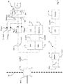
- the figure 3 partially and schematically represents an embodiment of a module 30 of a switched accumulator battery.
- the module 30 comprises all the elements of the module 10 described above, only the transistors HG, HD, BG and BD, the accumulator Acc 1 , the control circuit 14, the control circuit 16 and the sensors 18 being represented in figure 3 .
- the module 30 comprises a circuit 32 for supplying a supply voltage ALIM1 from the voltage at the terminals of one of the accumulators of the module 30.
- the supply voltage ALIM1 to be referenced to ground
- the supply voltage ALIM1 is supplied by the supply circuit 32 from the voltage V 1 at the terminals of the accumulator Acc 1 .
- the supply circuit 32 comprises a voltage step-up circuit 34 (Boost) receiving the voltage V 1 at the terminals of the accumulator Acc 1 and controlled by a signal Cmd1, and a voltage regulation circuit 36 (REG) receiving the voltage supplied by the step-up circuit 34 and supplying the voltage ALIM1.
- the control signal Cmd1 is supplied by the control circuit 14.
- the signal Cmd1 is a binary signal.
- the control signal Cmd1 is in a first state, for example the high state, the circuit 34 is activated and the supply circuit 32 supplies the voltage ALIM1.
- the control signal Cmd1 is in a second state, for example the low state, the circuit 34 is deactivated and the supply circuit 32 no longer supplies a supply voltage.
- the supply voltage ALIM1 is used only for supplying the control circuit 16.
- the module 30 further comprises a galvanically isolated DC-DC voltage converter 38 connected to a BUS supply bus and supplying a voltage ALIM2 from the voltage supplied by the BUS supply bus.
- the BUS power supply bus is not part of the module 30, the physical limit of the module 30 being shown schematically in figure 3 by a dashed line 40.
- the power supply bus BUS can be connected to each module 30 of the battery.
- the module 30 comprises a voltage regulation circuit 42 (REG) connected to the converter 38 and supplying a supply voltage ALIM3 to the control circuit 14.
- the module 30 further comprises a voltage regulation circuit 44 (REG) connected to the control circuit. converter 38 and supplying a supply voltage ALIM4 to the sensors 18.
- the module 30 comprises a diode D BD1 whose anode is connected to the driving circuit 16 and receives the signal Cmd BD and whose cathode is connected to the gate of the transistor BD.
- the module 30 further comprises a diode D BD2 , the anode of which is connected to the converter 38 by means of a switch SW and the cathode of which is connected to the gate of the transistor BD.
- the module 30 comprises a diode D BG1 whose anode is connected to the driving circuit 16 and receives the signal Cmd BG and whose cathode is connected to the gate of the transistor BG.
- the module 30 further comprises a diode D BG2 , the anode of which is connected to the converter 38 via the switch SW and the cathode of which is connected to the gate of the transistor BG.
- the switch SW is controlled by a signal Cmd2.
- the control signal Cmd2 is supplied by the control circuit 14.
- the signal Cmd2 is a binary signal.
- the switch SW can be produced by a MOS transistor.
- the signals Cmd1 and Cmd2 can be complementary.
- the diodes D BD1 and D BD2 constitute a first block implementing the OR logic function.
- the voltage at the gate of transistor BD, constituting the output of the first block is substantially equal to the highest voltage among the voltages at the level of the anodes of diodes D BD1 and D BD2 , constituting the inputs of the first block.
- the diodes D BG1 and D BG2 constitute a second block implementing the OR logic function.
- the voltage at the gate of transistor BG, constituting the output of the second block is substantially equal to the highest voltage among the voltages at the level of the anodes of diodes D BG1 and D BG2 , constituting the inputs of the second block.
- the supply voltage V 1 is for example between 1 V and 4 V depending on the type of accumulator Acc 1 , for example equal to approximately 2 V or 3.6 V.
- the voltage supplied by the step-up circuit 34 is by example between 2 V and 4 V, for example equal to approximately 3.8 V.
- the supply voltage ALIM1 is for example between 2 V and 4 V, for example equal to approximately 3.3 V.
- the control signals supplied by the control circuit 14 to the control circuit 16 can be binary signals alternating between a first level, for example at 0 V and a second level, for example at 3.3 V.
- the voltage supplied by the supply bus BUS can be between 4 V and 30 V, for example equal to 5 V, 12 V or 24 V.
- the voltage ALIM2 supplied by the converter 38 can be between 4 V and 30 V, for example equal to 5 V, 12 V or 24 V.
- the voltage ALIM2 is between 4 V and 5 V, which makes it possible to have few losses for the supply of control circuit 1 4 while making it possible to properly close the switch SW, in particular when the switch SW corresponds to a power switch.
- the figure 4 represents a timing diagram illustrating the operation of the battery module 30 according to the embodiment of the figure 3 . Times t0, t1 and t2 are successive times.
- the control circuit 14 when the accumulator Acc 1 operates normally (from time t0 to time t1 in figure 4 ), the control circuit 14 supplies the signal Cmd1 in the high state so that the circuit 34 is activated and the control circuit 14 supplies the signal Cmd2 in the low state so that the switch SW is open.
- the control circuit 16 is then supplied by the voltage ALIM1 and the switches BG and BD receive at their gate respectively the signals Cmd BG and Cmd BD .
- the voltage U supplied by the module 30 then depends on the control signals Cmd HG , Cmd HD , Cmd BG and Cmd BD .
- the control circuit 14 is suitable for detecting the failure of the accumulator Acc 1 and / or of the control circuit 16.
- the control circuit 14 can detect that the voltage V1 decreases below a threshold. given.
- the control circuit 14 then supplies the signal Cmd1 in the low state so that the circuit 34 is deactivated and the control circuit 14 supplies the signal Cmd2 in the high state so that the switch SW is closed.
- the control circuit 16 is then no longer supplied and the switches BG and BD receive the voltage ALIM2 at their gate.
- control signals Cmd HG , Cmd HD , Cmd BG and Cmd BD are in the low state.
- HD and HG transistors are therefore blocking.
- the gates of the transistors HD and HG receiving the voltage ALIM2, the transistors BD and BG are on.
- the voltage U is therefore substantially zero.
- An advantage of the embodiment of the module 30 is that the converter 38 is not used for supplying the control circuit 16 but only for supplying the control circuit 14, the sensors 18 and, in the event of failure of the control circuit. the supply of the control circuit 16, to control the closing of the switches BG and BD of the H-bridge. The converter 38 must therefore supply an electrical power lower than that which would be necessary if it were to supply the control circuit 16. A converter 38 with small footprint and low manufacturing cost can be used.
- Another advantage of the embodiment of the module 30 is that, in the event of a failure of the power supply to the driving circuit 16 of one of the battery modules, the switches BD and BG of this module are controlled so that the voltage U is substantially zero. The battery can therefore continue to operate.
- the failure of one of the modules leads to the stopping of the operation of the battery while with the embodiment of the module 30, the failure of one of the modules. battery can continue to operate.
- Another advantage of the embodiment of the module 30 is that the power supply for the control circuit 14 and the sensors 18 is separate from the power supply for the control circuit 16. This makes it possible to reduce the disturbances on the measurements made by the sensors 18. .
Landscapes
- Engineering & Computer Science (AREA)
- Power Engineering (AREA)
- Charge And Discharge Circuits For Batteries Or The Like (AREA)
- Secondary Cells (AREA)
Claims (7)
- Ein elektrisches System mit geschalteten Zellen, das Folgendes aufweist:einen Stromversorgungsbus (BUS);eine Anordnung von elektrischen Zellen (Acc1) und von ersten Schaltern (S1, B1), die die Zellen miteinander verbinden;zweite Schalter (HG, HD, BG, BD), die eine H-Brücke bilden und die Anordnung mit Knoten (V+, V-) verbinden;eine erste Schaltung (16) zum Liefern von ersten Steuersignalen (CmdHG, CmdHD, CmdBG, CmdBD, CmdS1, CmdB1) an die ersten Schalter und die zweiten Schalter;eine zweite Schaltung (32) zum Liefern einer ersten Stromversorgungsspannung (ALIM1) an die erste Schaltung auf der Grundlage der Spannung (V1) an einer der Zellen;eine dritte Schaltung (38, SW) zum Liefern von zweiten Steuersignalen (ALIM2) an mindestens zwei der zweiten Schalter (BG, BD), die mit dem Stromversorgungsbus verbunden ist; underste Dioden (DBD1, DBG1), die die erste Schaltung mit den mindestens zwei der zweiten Schalter verbinden, und zweite Dioden (DBD2, DBG2), die die dritte Schaltung mit den mindestens zwei der zweiten Schalter verbinden.
- Elektrisches System mit geschalteten Zellen nach Anspruch 1, wobei die dritte Schaltung (38, SW) einen isolierten Wandler (38) einer Gleichspannung in eine Gleichspannung aufweist, der mit dem Stromversorgungsbus (BUS) gekoppelt ist und eine zweite Stromversorgungsspannung (ALIM2) liefern kann.
- Elektrisches System mit geschalteten Zellen nach Anspruch 2, das eine vierte Schaltung (14) aufweist, die von der zweiten Versorgungsspannung (ALIM2) gespeist wird und die erste Schaltung (16) steuern kann.
- Elektrisches System mit geschalteten Zellen nach Anspruch 3, wobei die dritte Schaltung (38, SW) einen dritten Schalter (SW) zwischen dem isolierten Wandler (38) und den zweiten Dioden (DBD2, DBG2) aufweist, wobei der dritte Schalter von der vierten Schaltung (14) gesteuert wird.
- Elektrisches System mit geschalteten Zellen nach Anspruch 3 oder 4, wobei die vierte Schaltung (14) in der Lage ist, die Aktivierung oder die Deaktivierung der zweiten Schaltung (32) zu steuern.
- Elektrisches System mit geschalteten Zellen nach einem der Ansprüche 2 bis 5, mit Sensoren (18), die von der zweiten Versorgungsspannung (ALIM2) gespeist werden.
- Verfahren zur Verwendung des elektrischen Systems nach einem der Ansprüche 1 bis 6, das die folgenden aufeinanderfolgenden Schritte aufweist:Erkennen des Ausfalls der genannten einen Zelle (Acc1);Deaktivieren der zweiten Schaltung (32); undSteuern der mindestens zwei der zweiten Schalter (BG, BD) mit den zweiten Steuersignalen (ALIM2).
Applications Claiming Priority (2)
| Application Number | Priority Date | Filing Date | Title |
|---|---|---|---|
| FR1761991A FR3074976B1 (fr) | 2017-12-12 | 2017-12-12 | Batterie a accumulateurs commutes |
| PCT/FR2018/053145 WO2019115916A1 (fr) | 2017-12-12 | 2018-12-06 | Batterie a accumulateurs commutes |
Publications (2)
| Publication Number | Publication Date |
|---|---|
| EP3724963A1 EP3724963A1 (de) | 2020-10-21 |
| EP3724963B1 true EP3724963B1 (de) | 2021-09-15 |
Family
ID=61873427
Family Applications (1)
| Application Number | Title | Priority Date | Filing Date |
|---|---|---|---|
| EP18833269.6A Active EP3724963B1 (de) | 2017-12-12 | 2018-12-06 | Batterie mit geschalteten akkumulatoren |
Country Status (6)
| Country | Link |
|---|---|
| US (1) | US11362534B2 (de) |
| EP (1) | EP3724963B1 (de) |
| CA (1) | CA3085328A1 (de) |
| ES (1) | ES2900349T3 (de) |
| FR (1) | FR3074976B1 (de) |
| WO (1) | WO2019115916A1 (de) |
Families Citing this family (3)
| Publication number | Priority date | Publication date | Assignee | Title |
|---|---|---|---|---|
| US20210249872A1 (en) * | 2020-02-06 | 2021-08-12 | Samsung Sdi Co., Ltd. | Battery system |
| DE102020119340A1 (de) * | 2020-07-22 | 2022-01-27 | Phoenix Contact Gmbh & Co. Kg | Strommessgerät zur Messwerterfassung, Stromsensor sowie Strommessumformer |
| CN114142723B (zh) * | 2022-02-05 | 2022-04-26 | 伏达半导体(合肥)有限公司 | 电源转换结构及包括其的电子设备 |
Family Cites Families (7)
| Publication number | Priority date | Publication date | Assignee | Title |
|---|---|---|---|---|
| US6700802B2 (en) * | 2000-02-14 | 2004-03-02 | Aura Systems, Inc. | Bi-directional power supply circuit |
| FR2977986B1 (fr) * | 2011-07-13 | 2014-04-25 | Commissariat Energie Atomique | Batterie avec architecture en briques disposees en serie ou en parallele |
| FR2972304A1 (fr) * | 2011-03-02 | 2012-09-07 | Commissariat Energie Atomique | Batterie avec gestion individuelle des cellules |
| FR2972306A1 (fr) | 2011-03-02 | 2012-09-07 | Commissariat Energie Atomique | Batterie avec gestion individuelle des cellules |
| CN103066633B (zh) * | 2011-10-18 | 2015-11-18 | 丁景信 | 电源管理系统 |
| CN103107689A (zh) * | 2011-11-11 | 2013-05-15 | 台达电子企业管理(上海)有限公司 | 一种级联型变频器、功率单元及其旁路模块 |
| KR102201102B1 (ko) * | 2013-03-15 | 2021-01-12 | 디자인 플럭스 테크놀로지스, 엘엘씨 | 동적으로 재구성가능한 에너지 스토리지 장치를 생성하기 위한 방법 및 장치 |
-
2017
- 2017-12-12 FR FR1761991A patent/FR3074976B1/fr not_active Expired - Fee Related
-
2018
- 2018-12-06 WO PCT/FR2018/053145 patent/WO2019115916A1/fr not_active Ceased
- 2018-12-06 US US16/772,103 patent/US11362534B2/en active Active
- 2018-12-06 EP EP18833269.6A patent/EP3724963B1/de active Active
- 2018-12-06 ES ES18833269T patent/ES2900349T3/es active Active
- 2018-12-06 CA CA3085328A patent/CA3085328A1/fr active Pending
Also Published As
| Publication number | Publication date |
|---|---|
| FR3074976A1 (fr) | 2019-06-14 |
| WO2019115916A1 (fr) | 2019-06-20 |
| US11362534B2 (en) | 2022-06-14 |
| ES2900349T3 (es) | 2022-03-16 |
| US20200335982A1 (en) | 2020-10-22 |
| EP3724963A1 (de) | 2020-10-21 |
| FR3074976B1 (fr) | 2019-12-20 |
| CA3085328A1 (fr) | 2019-06-20 |
Similar Documents
| Publication | Publication Date | Title |
|---|---|---|
| EP2532070B1 (de) | Ausgleichssystem für akkumulatoren | |
| EP2944008B1 (de) | Ladungsausgleich innerhalb einer elektrischen batterie | |
| WO2011101555A1 (fr) | Systeme d'equilibrage par couplage magnetique d'une association serie d'elements de generation ou de stockage d'energie electrique | |
| EP3724963B1 (de) | Batterie mit geschalteten akkumulatoren | |
| FR3097089A1 (fr) | Un convertisseur et son systeme de controle de courant | |
| CA3102416A1 (fr) | Systeme electrique a cellules commutees et procede de commande d'un tel systeme | |
| US10658856B1 (en) | Battery pack and discharge method for limiting an excessive discharge current | |
| TW202013853A (zh) | 電池管理方法以及電源系統 | |
| FR3015805A1 (fr) | Hacheur elevateur entrelace a commutation douce | |
| EP3171482B1 (de) | Elektrische batterie, die ein elektronisches steuerungssystem umfasst | |
| EP3732763B1 (de) | Batteriepack | |
| EP3732766A1 (de) | Batteriepack | |
| US11398743B2 (en) | Apparatus and method for forming current path according to charging or discharging state of battery pack | |
| FR3072519A1 (fr) | Procede de conversion d'energie entre deux dispositifs usb type c et dispositif correspondant | |
| EP3724962B1 (de) | Batterie mit geschalteten akkumulatoren | |
| WO2005031943A1 (fr) | Module de transfert de charges entre deux dipoles | |
| JPH1146450A (ja) | 太陽電池式電源装置 | |
| FR3059167A1 (fr) | Systeme d'equilibrage local analogique pour un ensemble de dispositifs de stockage d'energie electrique par effet capacitif, module de stockage rechargeable, vehicule de transport et installation electriques comprenant un tel systeme. | |
| WO2022180346A1 (fr) | Dispositif de stockage et de génération concomitante d'au moins une tension électrique, et procédé de gestion associé | |
| EP3732762B1 (de) | Batteriepack | |
| WO2021250254A1 (fr) | Convertisseur de tension dc/dc avec dispositif de precharge | |
| JPH1146451A (ja) | 太陽電池式電源装置 | |
| EP2203971B1 (de) | Verfahren zur steuerung eines schaltnetzteils und entsprechendes netzteil | |
| EP3289691A1 (de) | Verfahren zum austausch von daten zwischen zwei elektromechanischen vorrichtungen | |
| WO2021044017A1 (fr) | Association de transistors |
Legal Events
| Date | Code | Title | Description |
|---|---|---|---|
| STAA | Information on the status of an ep patent application or granted ep patent |
Free format text: STATUS: UNKNOWN |
|
| STAA | Information on the status of an ep patent application or granted ep patent |
Free format text: STATUS: THE INTERNATIONAL PUBLICATION HAS BEEN MADE |
|
| PUAI | Public reference made under article 153(3) epc to a published international application that has entered the european phase |
Free format text: ORIGINAL CODE: 0009012 |
|
| STAA | Information on the status of an ep patent application or granted ep patent |
Free format text: STATUS: REQUEST FOR EXAMINATION WAS MADE |
|
| 17P | Request for examination filed |
Effective date: 20200629 |
|
| AK | Designated contracting states |
Kind code of ref document: A1 Designated state(s): AL AT BE BG CH CY CZ DE DK EE ES FI FR GB GR HR HU IE IS IT LI LT LU LV MC MK MT NL NO PL PT RO RS SE SI SK SM TR |
|
| AX | Request for extension of the european patent |
Extension state: BA ME |
|
| DAV | Request for validation of the european patent (deleted) | ||
| DAX | Request for extension of the european patent (deleted) | ||
| GRAP | Despatch of communication of intention to grant a patent |
Free format text: ORIGINAL CODE: EPIDOSNIGR1 |
|
| STAA | Information on the status of an ep patent application or granted ep patent |
Free format text: STATUS: GRANT OF PATENT IS INTENDED |
|
| INTG | Intention to grant announced |
Effective date: 20210528 |
|
| GRAS | Grant fee paid |
Free format text: ORIGINAL CODE: EPIDOSNIGR3 |
|
| GRAA | (expected) grant |
Free format text: ORIGINAL CODE: 0009210 |
|
| STAA | Information on the status of an ep patent application or granted ep patent |
Free format text: STATUS: THE PATENT HAS BEEN GRANTED |
|
| AK | Designated contracting states |
Kind code of ref document: B1 Designated state(s): AL AT BE BG CH CY CZ DE DK EE ES FI FR GB GR HR HU IE IS IT LI LT LU LV MC MK MT NL NO PL PT RO RS SE SI SK SM TR |
|
| REG | Reference to a national code |
Ref country code: CH Ref legal event code: EP |
|
| REG | Reference to a national code |
Ref country code: DE Ref legal event code: R096 Ref document number: 602018023745 Country of ref document: DE |
|
| REG | Reference to a national code |
Ref country code: IE Ref legal event code: FG4D Free format text: LANGUAGE OF EP DOCUMENT: FRENCH |
|
| REG | Reference to a national code |
Ref country code: AT Ref legal event code: REF Ref document number: 1431278 Country of ref document: AT Kind code of ref document: T Effective date: 20211015 |
|
| REG | Reference to a national code |
Ref country code: NL Ref legal event code: FP |
|
| REG | Reference to a national code |
Ref country code: LT Ref legal event code: MG9D |
|
| PG25 | Lapsed in a contracting state [announced via postgrant information from national office to epo] |
Ref country code: HR Free format text: LAPSE BECAUSE OF FAILURE TO SUBMIT A TRANSLATION OF THE DESCRIPTION OR TO PAY THE FEE WITHIN THE PRESCRIBED TIME-LIMIT Effective date: 20210915 Ref country code: NO Free format text: LAPSE BECAUSE OF FAILURE TO SUBMIT A TRANSLATION OF THE DESCRIPTION OR TO PAY THE FEE WITHIN THE PRESCRIBED TIME-LIMIT Effective date: 20211215 Ref country code: BG Free format text: LAPSE BECAUSE OF FAILURE TO SUBMIT A TRANSLATION OF THE DESCRIPTION OR TO PAY THE FEE WITHIN THE PRESCRIBED TIME-LIMIT Effective date: 20211215 Ref country code: LT Free format text: LAPSE BECAUSE OF FAILURE TO SUBMIT A TRANSLATION OF THE DESCRIPTION OR TO PAY THE FEE WITHIN THE PRESCRIBED TIME-LIMIT Effective date: 20210915 Ref country code: SE Free format text: LAPSE BECAUSE OF FAILURE TO SUBMIT A TRANSLATION OF THE DESCRIPTION OR TO PAY THE FEE WITHIN THE PRESCRIBED TIME-LIMIT Effective date: 20210915 Ref country code: RS Free format text: LAPSE BECAUSE OF FAILURE TO SUBMIT A TRANSLATION OF THE DESCRIPTION OR TO PAY THE FEE WITHIN THE PRESCRIBED TIME-LIMIT Effective date: 20210915 Ref country code: FI Free format text: LAPSE BECAUSE OF FAILURE TO SUBMIT A TRANSLATION OF THE DESCRIPTION OR TO PAY THE FEE WITHIN THE PRESCRIBED TIME-LIMIT Effective date: 20210915 |
|
| REG | Reference to a national code |
Ref country code: AT Ref legal event code: MK05 Ref document number: 1431278 Country of ref document: AT Kind code of ref document: T Effective date: 20210915 |
|
| PG25 | Lapsed in a contracting state [announced via postgrant information from national office to epo] |
Ref country code: LV Free format text: LAPSE BECAUSE OF FAILURE TO SUBMIT A TRANSLATION OF THE DESCRIPTION OR TO PAY THE FEE WITHIN THE PRESCRIBED TIME-LIMIT Effective date: 20210915 Ref country code: GR Free format text: LAPSE BECAUSE OF FAILURE TO SUBMIT A TRANSLATION OF THE DESCRIPTION OR TO PAY THE FEE WITHIN THE PRESCRIBED TIME-LIMIT Effective date: 20211216 |
|
| REG | Reference to a national code |
Ref country code: ES Ref legal event code: FG2A Ref document number: 2900349 Country of ref document: ES Kind code of ref document: T3 Effective date: 20220316 |
|
| PG25 | Lapsed in a contracting state [announced via postgrant information from national office to epo] |
Ref country code: AT Free format text: LAPSE BECAUSE OF FAILURE TO SUBMIT A TRANSLATION OF THE DESCRIPTION OR TO PAY THE FEE WITHIN THE PRESCRIBED TIME-LIMIT Effective date: 20210915 |
|
| PG25 | Lapsed in a contracting state [announced via postgrant information from national office to epo] |
Ref country code: IS Free format text: LAPSE BECAUSE OF FAILURE TO SUBMIT A TRANSLATION OF THE DESCRIPTION OR TO PAY THE FEE WITHIN THE PRESCRIBED TIME-LIMIT Effective date: 20220115 Ref country code: SM Free format text: LAPSE BECAUSE OF FAILURE TO SUBMIT A TRANSLATION OF THE DESCRIPTION OR TO PAY THE FEE WITHIN THE PRESCRIBED TIME-LIMIT Effective date: 20210915 Ref country code: SK Free format text: LAPSE BECAUSE OF FAILURE TO SUBMIT A TRANSLATION OF THE DESCRIPTION OR TO PAY THE FEE WITHIN THE PRESCRIBED TIME-LIMIT Effective date: 20210915 Ref country code: RO Free format text: LAPSE BECAUSE OF FAILURE TO SUBMIT A TRANSLATION OF THE DESCRIPTION OR TO PAY THE FEE WITHIN THE PRESCRIBED TIME-LIMIT Effective date: 20210915 Ref country code: PT Free format text: LAPSE BECAUSE OF FAILURE TO SUBMIT A TRANSLATION OF THE DESCRIPTION OR TO PAY THE FEE WITHIN THE PRESCRIBED TIME-LIMIT Effective date: 20220117 Ref country code: PL Free format text: LAPSE BECAUSE OF FAILURE TO SUBMIT A TRANSLATION OF THE DESCRIPTION OR TO PAY THE FEE WITHIN THE PRESCRIBED TIME-LIMIT Effective date: 20210915 Ref country code: EE Free format text: LAPSE BECAUSE OF FAILURE TO SUBMIT A TRANSLATION OF THE DESCRIPTION OR TO PAY THE FEE WITHIN THE PRESCRIBED TIME-LIMIT Effective date: 20210915 Ref country code: CZ Free format text: LAPSE BECAUSE OF FAILURE TO SUBMIT A TRANSLATION OF THE DESCRIPTION OR TO PAY THE FEE WITHIN THE PRESCRIBED TIME-LIMIT Effective date: 20210915 Ref country code: AL Free format text: LAPSE BECAUSE OF FAILURE TO SUBMIT A TRANSLATION OF THE DESCRIPTION OR TO PAY THE FEE WITHIN THE PRESCRIBED TIME-LIMIT Effective date: 20210915 |
|
| REG | Reference to a national code |
Ref country code: DE Ref legal event code: R097 Ref document number: 602018023745 Country of ref document: DE |
|
| PLBE | No opposition filed within time limit |
Free format text: ORIGINAL CODE: 0009261 |
|
| STAA | Information on the status of an ep patent application or granted ep patent |
Free format text: STATUS: NO OPPOSITION FILED WITHIN TIME LIMIT |
|
| PG25 | Lapsed in a contracting state [announced via postgrant information from national office to epo] |
Ref country code: MC Free format text: LAPSE BECAUSE OF FAILURE TO SUBMIT A TRANSLATION OF THE DESCRIPTION OR TO PAY THE FEE WITHIN THE PRESCRIBED TIME-LIMIT Effective date: 20210915 Ref country code: DK Free format text: LAPSE BECAUSE OF FAILURE TO SUBMIT A TRANSLATION OF THE DESCRIPTION OR TO PAY THE FEE WITHIN THE PRESCRIBED TIME-LIMIT Effective date: 20210915 |
|
| REG | Reference to a national code |
Ref country code: CH Ref legal event code: PL |
|
| 26N | No opposition filed |
Effective date: 20220616 |
|
| PG25 | Lapsed in a contracting state [announced via postgrant information from national office to epo] |
Ref country code: SI Free format text: LAPSE BECAUSE OF FAILURE TO SUBMIT A TRANSLATION OF THE DESCRIPTION OR TO PAY THE FEE WITHIN THE PRESCRIBED TIME-LIMIT Effective date: 20210915 |
|
| PG25 | Lapsed in a contracting state [announced via postgrant information from national office to epo] |
Ref country code: IE Free format text: LAPSE BECAUSE OF NON-PAYMENT OF DUE FEES Effective date: 20211206 |
|
| PG25 | Lapsed in a contracting state [announced via postgrant information from national office to epo] |
Ref country code: LI Free format text: LAPSE BECAUSE OF NON-PAYMENT OF DUE FEES Effective date: 20211231 Ref country code: CH Free format text: LAPSE BECAUSE OF NON-PAYMENT OF DUE FEES Effective date: 20211231 |
|
| PG25 | Lapsed in a contracting state [announced via postgrant information from national office to epo] |
Ref country code: CY Free format text: LAPSE BECAUSE OF FAILURE TO SUBMIT A TRANSLATION OF THE DESCRIPTION OR TO PAY THE FEE WITHIN THE PRESCRIBED TIME-LIMIT Effective date: 20210915 |
|
| PG25 | Lapsed in a contracting state [announced via postgrant information from national office to epo] |
Ref country code: HU Free format text: LAPSE BECAUSE OF FAILURE TO SUBMIT A TRANSLATION OF THE DESCRIPTION OR TO PAY THE FEE WITHIN THE PRESCRIBED TIME-LIMIT; INVALID AB INITIO Effective date: 20181206 |
|
| PG25 | Lapsed in a contracting state [announced via postgrant information from national office to epo] |
Ref country code: MK Free format text: LAPSE BECAUSE OF FAILURE TO SUBMIT A TRANSLATION OF THE DESCRIPTION OR TO PAY THE FEE WITHIN THE PRESCRIBED TIME-LIMIT Effective date: 20210915 |
|
| PG25 | Lapsed in a contracting state [announced via postgrant information from national office to epo] |
Ref country code: TR Free format text: LAPSE BECAUSE OF FAILURE TO SUBMIT A TRANSLATION OF THE DESCRIPTION OR TO PAY THE FEE WITHIN THE PRESCRIBED TIME-LIMIT Effective date: 20210915 |
|
| PG25 | Lapsed in a contracting state [announced via postgrant information from national office to epo] |
Ref country code: MT Free format text: LAPSE BECAUSE OF FAILURE TO SUBMIT A TRANSLATION OF THE DESCRIPTION OR TO PAY THE FEE WITHIN THE PRESCRIBED TIME-LIMIT Effective date: 20210915 |
|
| PGFP | Annual fee paid to national office [announced via postgrant information from national office to epo] |
Ref country code: BE Payment date: 20241227 Year of fee payment: 7 Ref country code: NL Payment date: 20241227 Year of fee payment: 7 Ref country code: LU Payment date: 20241216 Year of fee payment: 7 |
|
| PGFP | Annual fee paid to national office [announced via postgrant information from national office to epo] |
Ref country code: IT Payment date: 20241216 Year of fee payment: 7 |
|
| PGFP | Annual fee paid to national office [announced via postgrant information from national office to epo] |
Ref country code: ES Payment date: 20250117 Year of fee payment: 7 |
|
| PGFP | Annual fee paid to national office [announced via postgrant information from national office to epo] |
Ref country code: GB Payment date: 20251229 Year of fee payment: 8 |
|
| PGFP | Annual fee paid to national office [announced via postgrant information from national office to epo] |
Ref country code: FR Payment date: 20251222 Year of fee payment: 8 |
|
| PGFP | Annual fee paid to national office [announced via postgrant information from national office to epo] |
Ref country code: DE Payment date: 20251222 Year of fee payment: 8 |