EP3726268A1 - Reflektorvorrichtung - Google Patents
Reflektorvorrichtung Download PDFInfo
- Publication number
- EP3726268A1 EP3726268A1 EP20169780.2A EP20169780A EP3726268A1 EP 3726268 A1 EP3726268 A1 EP 3726268A1 EP 20169780 A EP20169780 A EP 20169780A EP 3726268 A1 EP3726268 A1 EP 3726268A1
- Authority
- EP
- European Patent Office
- Prior art keywords
- layer
- light radiation
- front face
- mirror
- rear face
- Prior art date
- Legal status (The legal status is an assumption and is not a legal conclusion. Google has not performed a legal analysis and makes no representation as to the accuracy of the status listed.)
- Granted
Links
Images




Classifications
-
- G—PHYSICS
- G02—OPTICS
- G02B—OPTICAL ELEMENTS, SYSTEMS OR APPARATUS
- G02B7/00—Mountings, adjusting means, or light-tight connections, for optical elements
- G02B7/008—Mountings, adjusting means, or light-tight connections, for optical elements with means for compensating for changes in temperature or for controlling the temperature; thermal stabilisation
-
- G—PHYSICS
- G01—MEASURING; TESTING
- G01S—RADIO DIRECTION-FINDING; RADIO NAVIGATION; DETERMINING DISTANCE OR VELOCITY BY USE OF RADIO WAVES; LOCATING OR PRESENCE-DETECTING BY USE OF THE REFLECTION OR RERADIATION OF RADIO WAVES; ANALOGOUS ARRANGEMENTS USING OTHER WAVES
- G01S7/00—Details of systems according to groups G01S13/00, G01S15/00, G01S17/00
- G01S7/48—Details of systems according to groups G01S13/00, G01S15/00, G01S17/00 of systems according to group G01S17/00
- G01S7/481—Constructional features, e.g. arrangements of optical elements
- G01S7/4817—Constructional features, e.g. arrangements of optical elements relating to scanning
-
- G—PHYSICS
- G02—OPTICS
- G02B—OPTICAL ELEMENTS, SYSTEMS OR APPARATUS
- G02B26/00—Optical devices or arrangements for the control of light using movable or deformable optical elements
- G02B26/08—Optical devices or arrangements for the control of light using movable or deformable optical elements for controlling the direction of light
- G02B26/0816—Optical devices or arrangements for the control of light using movable or deformable optical elements for controlling the direction of light by means of one or more reflecting elements
- G02B26/0833—Optical devices or arrangements for the control of light using movable or deformable optical elements for controlling the direction of light by means of one or more reflecting elements the reflecting element being a micromechanical device, e.g. a MEMS mirror, DMD
-
- G—PHYSICS
- G02—OPTICS
- G02B—OPTICAL ELEMENTS, SYSTEMS OR APPARATUS
- G02B5/00—Optical elements other than lenses
- G02B5/003—Light absorbing elements
-
- G—PHYSICS
- G02—OPTICS
- G02B—OPTICAL ELEMENTS, SYSTEMS OR APPARATUS
- G02B5/00—Optical elements other than lenses
- G02B5/02—Diffusing elements; Afocal elements
- G02B5/0205—Diffusing elements; Afocal elements characterised by the diffusing properties
-
- G—PHYSICS
- G02—OPTICS
- G02B—OPTICAL ELEMENTS, SYSTEMS OR APPARATUS
- G02B5/00—Optical elements other than lenses
- G02B5/02—Diffusing elements; Afocal elements
- G02B5/0205—Diffusing elements; Afocal elements characterised by the diffusing properties
- G02B5/021—Diffusing elements; Afocal elements characterised by the diffusing properties the diffusion taking place at the element's surface, e.g. by means of surface roughening or microprismatic structures
- G02B5/0226—Diffusing elements; Afocal elements characterised by the diffusing properties the diffusion taking place at the element's surface, e.g. by means of surface roughening or microprismatic structures having particles on the surface
-
- G—PHYSICS
- G02—OPTICS
- G02B—OPTICAL ELEMENTS, SYSTEMS OR APPARATUS
- G02B5/00—Optical elements other than lenses
- G02B5/02—Diffusing elements; Afocal elements
Definitions
- the invention relates to a reflector device, and in particular to a reflector device which undergoes little or no heating during operation.
- the reflector device comprises a partially transparent mirror and behind which are arranged means for thermal diffusion and / or absorption.
- Micro-mirrors are widely present today in the MEMS field and in particular in devices of the LIDAR type (“Light Detection And Ranging systems”).
- the latter make it possible in particular to scan a surface or a target with light radiation for the purposes of detection or imaging.
- the micro-mirrors are arranged to oscillate along one or two pivot axis (s), at a predetermined beat frequency, so as to reflect incident radiation in different directions.
- the beat frequency of the micro-mirrors can vary from a few Hz to several kHz, and their size can be of the order of a few millimeters (for example a few millimeters in diameter for disk-shaped micro-mirrors), and can in particular be between 1 mm and 3 mm.
- a micromirror can comprise a metallic reflective layer formed on a main face of a support, for example a support made of silicon, and in particular of monocrystalline silicon.
- the metallic reflective layer can in particular comprise a layer of gold or aluminum with a thickness between 50 nm and 500 nm.
- the metallic reflective layer has a non-negligible absorption coefficient of light radiation so that in operation, in particular when the power of the incident radiation is high, heating of the micromirror is observed.
- a micromirror comprising a reflective metallic layer having a reflection coefficient of 96% and an absorption coefficient of 4% may undergo a temperature increase sufficient to lead to the thermomechanical destruction of the mirror
- a micro-mirror comprising a reflective metal layer having a reflection coefficient of 98% and an absorption coefficient of the order of 2% may undergo a “theoretical” heating to a temperature close to 2000 ° C after a hundred seconds
- Such a Bragg reflector stack generally comprises a plurality of elementary reflector stacks arranged to reflect radiation of a predetermined wavelength called the Bragg length.
- a Bragg stack intended to operate at the Bragg length equal to 1550 nm, may comprise a layer of amorphous silicon 110 nm thick and a layer of silicon dioxide 305 nm thick. .
- the Bragg reflector stack is little or no absorbent so that no heating of the micro-mirror is observed.
- the latter in order to maximize the reflection coefficient of the Bragg reflector stack, the latter generally comprises a large number elementary reflective stacks which can be the source of deformations due to the mechanical stresses imposed by the multiplication of layers.
- the multiplication of elementary stacks also complicates the method of manufacturing such a reflector.
- the consideration of a reduced number of elementary reflector stacks affects the reflection coefficient of the micro-mirror.
- the latter which is partially transparent, transmits part of the light radiation.
- An aim of the present invention is therefore to provide an optical device provided with a micro-mirror capable of operating at powers of incident radiation higher than the usual metallic mirrors, that is to say with a damage threshold laser higher both in the short term and in the long term.
- Another object of the present invention is also to provide an optical device provided with a micromirror and designed to limit the deformations of said mirror.
- the diffusion and / or absorption means are arranged opposite and at a distance from the rear face.
- the diffusion means comprise a series of first sampling blades, essentially flat or curved (allowing said first sampling blades to be divergent), called first blades, said first sampling blades each being provided a first front face and a first rear face opposite the first front face.
- These first blades are aligned in an alignment direction, parallel to each other, and oriented so as to partially reflect the light radiation capable of being transmitted by the rear face, in the direction of a first dissipator (heat sink).
- the first blades can for example reflect the light radiation capable of being emitted by the rear face at a reflection angle either close to 45 degrees, or close to 90 ° to said light radiation, and in the direction of the first dissipator.
- the advantage of the dissipation means according to this embodiment is to be able to dissipate the energy of the light radiation capable of being transmitted by the rear face at different points or different regions of the first dissipator. These means make it possible more particularly to "spread" the flux associated with the light radiation capable of being transmitted by the rear face.
- first blades can be more and more tightened as one moves away from the rear face.
- the intensity actually received on the first front face of a first given sampling slide is equal to T n x I 0 , where T is the transmission coefficient of a first sampling slide and n is the number of first sampling slides preceding the first given sampling slide on the path of the light radiation. Consequently, the adjustment of the spacing between first sampling blades is a function of T (T is less than 1, for example equal to 0.9), of I 0 , but also according to the heat dissipation property of the at least one heatsink.
- first slides can be very transparent and very little absorbent.
- the first plates can make it possible to reflect a few percent (for example 8%) of an incident radiation and to transmit a few tens of percent (for example 92%)
- the first plates can comprise glass for example a glass of the type B1664 , or BK7. The invention is not however limited to these two examples.
- the at least one first dissipator is arranged perpendicular to the front face of the mirror.
- the first sampling blades are also partially transparent so that the first front face of each of them is exposed to the light radiation capable of being transmitted by the rear face and passing through the first blade. sampling which precedes it on the path of the radiation.
- the diffusion means comprise a series of second sampling blades, for example of the same type as the first sampling blades, essentially flat or curved (allowing said first sampling blades to be divergent), said first blades, each provided with a second front face and a second rear face opposite the second front face, the second sampling blades being aligned in an alignment direction, parallel to each other, and oriented in a manner think about it in part, and in the direction of a second dissipator, the light radiation capable of being transmitted by the rear face.
- second sampling blades for example of the same type as the first sampling blades, essentially flat or curved (allowing said first sampling blades to be divergent)
- said first blades each provided with a second front face and a second rear face opposite the second front face, the second sampling blades being aligned in an alignment direction, parallel to each other, and oriented in a manner think about it in part, and in the direction of a second dissipator, the light radiation capable of being transmitted by the rear face.
- the first sampling blades and the second sampling blades are arranged alternately along the alignment direction.
- Sampling blades in a series may also be aligned in an alignment direction, parallel to each other, and oriented to reflect in part, and in the direction of another heatsink.
- the first dissipator, the second dissipator as well as the other dissipators likely to be considered can be arranged around the direction of alignment (in other words the direction of propagation of the light radiation coming from the rear face of the micro-mirror). For example, if three heatsinks were to be considered, the normal of the latter could be arranged angularly at 120 ° to each other around the alignment axis. It is possible to generalize this concept to N dissipators arranged angularly at 360 ° / N around the alignment axis.
- the device can also comprise at least a first divergent lens which is interposed between a first front face (of a first sampling blade) and the first dissipator so as to spread the radiation reflected by said first face towards said first dissipator.
- the device can also comprise at least one divergent second lens which is interposed between a second front face (of a second sampling blade) and the second dissipator so as to spread the radiation reflected by said second face towards said second heatsink.
- the first sampling blades are arranged perpendicular to the second sampling blades.
- the mirror comprises, from its front face to its rear face, a partially reflecting layer and a support layer mechanical, said layers each having an absorption coefficient at the wavelength ⁇ of less than 0.1%, advantageously zero.
- the partially reflecting layer comprises a Bragg stack, the Bragg stack comprising at least one elementary Bragg stack.
- an elementary Bragg stack comprises a stack of two dielectric and / or semiconductor layers, advantageously an elementary Bragg stack comprises a layer of silicon dioxide and a layer of amorphous silicon.
- the Bragg stack is limited to one or two elementary Bragg stacks.
- the invention is not however limited to the implementation of one or two elementary Bragg stacks, and a larger number of stacks can be considered insofar as the problem of curvature of the mirror is controlled.
- the mechanical support layer comprises a semiconductor material, advantageously silicon, even more advantageously monocrystalline silicon.
- a so-called impedance matching layer is configured to limit internal reflections of light radiation within the mirror.
- said device is a LIDAR device.
- the present invention relates to a reflector device provided with a mirror (or micro-mirror) intended to reflect light radiation of average and instantaneous optical powers higher than the usual metallic micro-mirrors without undergoing a significant rise in temperature and / or likely to degrade its performance, ie with higher laser damage thresholds than usual micro-mirrors.
- a mirror or micro-mirror
- the present invention therefore uses a mirror which absorbs little or no light radiation, coupled to means for heat dissipation of the light flux capable of being transmitted by this mirror.
- light scattering can be used interchangeably to describe both a scattering and an absorption of light radiation, or a deflection of said radiation or even a dissipation. thermal.
- diffuse is meant the deviation in several directions of a light radiation.
- absorb is meant the transformation of the energy carried by the light radiation into another form of energy so as to dissipate the latter.
- absorption coefficient is meant the proportion of incident energy, carried by the light radiation
- reflection coefficient is meant the proportion of incident energy, carried by the light radiation
- transmission coefficient is meant the proportion of incident energy, carried by the light radiation, transmitted
- deflection is understood to mean means configured to reorient the reflection of the radiation transmitted in a direction other than a rear face of the mirror.
- the figures 1 to 6 illustrate different embodiments of a reflector device 10 according to the present invention.
- the reflector device 10 can comprise holding means 21, for example two uprights 21a and 21b, intended to hold a mirror 23 partially transparent with regard to light radiation of a predetermined wavelength ⁇ .
- partially transparent it is understood that a fraction of a light radiation incident I on a front face 24 of the mirror is reflected by said face, while another fraction partly passes through the mirror, and comes out in the form of a mirror. transmitted radiation T, via a rear face 25 opposite to the front face 24.
- the holding means 21a and 21b can in particular be arranged to allow the mirror to pivot around one or two pivot axes.
- the device also comprises diffusion and / or absorption means 26 configured to diffuse and / or absorb the transmitted radiation.
- the scattering and / or absorption means 26 in particular limit the reflection of the radiation in the direction of the mirror 23.
- the diffusion and / or absorption means 26 can be arranged opposite and at a distance from the rear face 25 of the mirror 23.
- the holding means 21 extend from the diffusion means and / or absorption 26.
- the diffusion and / or absorption means 26 are arranged to absorb the transmitted radiation.
- the means 26 may comprise at least one absorbent layer 27 (or stack of absorbent layers), for example an absorbent metal layer formed on a main face 22 of a support 20, for example a silicon support.
- the absorbent layer may comprise a layer of a powder, in particular a layer of graphite powder.
- a layer of graphite powder is little or not transmissive, and also has a very low reflection coefficient (of the order of 0.5%) .
- the means 26 may comprise, on a support substrate (for example a silicon support substrate), and from one face of this support substrate, a layer of titanium 200 nm thick, a layer of silicon dioxide 270 nm thick, a layer of titanium 13 nm thick, and a layer of silicon dioxide 250 nm thick.
- a support substrate for example a silicon support substrate
- the means 26 may comprise, on a support substrate (for example a silicon support substrate), and from one face of this support substrate, a layer of titanium 200 nm thick, a layer of silicon dioxide 270 nm thick, a layer of titanium 13 nm thick, and a layer of silicon dioxide 250 nm thick.
- a support substrate for example a silicon support substrate
- the diffusion and / or absorption means 26 comprise a plate which may be metallic.
- this plate comprises a face facing the rear face 25, and the surface of which is textured 28 so as to distribute the transmitted radiation.
- Texturing the surface can in particular comprise the production of 3-dimensional patterns, for example according to a range of spatial periods adjusted to diffuse the light radiation of wavelength ⁇ .
- the spatial periods considered may be slightly greater than the predetermined wavelength ⁇ .
- the spatial period of the texturing may be between 2 ⁇ m and 5 ⁇ m.
- the diffusion plate may comprise an aluminum plate (the face of which facing the rear face 25 is textured).
- Texturing can also be obtained by dispersing a powder of a chosen particle size on one face of a support substrate.
- the diffusion and / or absorption means 26 may comprise a reflective plate, one face of which has a texturing 29, in particular protruding faceted shapes, intended to deflect the radiation transmitted in a direction other than that of the mirror.
- the protruding faceted shapes can in particular comprise pyramids (for example with 3 or 4 facets).
- the diffusion and / or absorption means 26 may comprise a layer of carbon nanotubes 30 formed on a support substrate, in particular a silicon substrate.
- the diffusion and / or absorption means 26 may comprise a heat sink 31, in particular a heat sink with anodized aluminum fins.
- the heat sink 31 can, in particular, be coupled to the reflector device 10 via an intermediate support 32.
- the diffusion and / or absorption means 26 comprises a heat dissipating device on which an anti-reflection layer is formed.
- the heat sink can in particular take the characteristics of the first or of the fifth embodiment.
- the anti-reflection layer can in particular be Aeroglaze Z-306®.
- the diffusion means 26 comprise a series of first sampling blades 34a, 34b, 34c, essentially flat or curved, each provided with a first front face 35a and a first rear face 35b opposite the first front face 35a.
- the first sampling blades 34a, 34b, 34c are in particular aligned in an alignment direction XX ', and parallel to each other. The latter are also oriented so as to reflect in part, and in the direction of a first dissipator 36, the light radiation capable of being transmitted by the rear face 25.
- the first dissipator 36 can for example be arranged perpendicular to the front face. 24 of mirror 23.
- the first sampling blades can be pivotally mounted.
- first sampling blades 34a, 34b, 34c can also be partially transparent so that the first front face 35a of each of them is exposed to the light radiation capable of being transmitted by the rear face 25 and passing through the first sampling blade which precedes it on the path of the radiation.
- first slides can be very transparent and very little absorbent.
- the first plates can make it possible to reflect a few percent (for example 8%) of an incident radiation and to transmit a few tens of percent (for example 92%)
- the first plates can comprise glass for example a glass of the type B1664 , or BK7. The invention is not however limited to these two examples.
- the mirror 23 can finally be surmounted by a transparent window 37 arranged on a base 38.
- the base 38 can have an opening intended to reveal the rear face of the mirror 23.
- the light radiation capable of being transmitted by a rear face 25 successively passes through the first blades of sample 34a, 34b and 34c. Part of this radiation is nevertheless reflected by each of the first front faces 35b in the direction of the dissipating screen 36.
- the implementation of several first sampling blades according to this seventh embodiment thus makes it possible to distribute at different places of the dissipating screen 36 the energy to be dissipated.
- This distribution is also dependent on the spacing between the first sampling blades.
- the latter may exhibit a decreasing spacing as one moves away from the rear face.
- the first sampling blades 34a, 34b, and 34c can comprise a glass, for example BK7, or silicon covered with an elementary Bragg stack comprising a layer of silicon dioxide and a layer of amorphous silicon.
- the first sampling blades 34a, 34b, and 34c may be square in shape of 5 mm by 5 mm side.
- the first heat sink 36 may be of square shape, for example 5 cm by 5 cm side.
- the first dissipator 36 may comprise a non-reflecting absorbent layer, by a powder layer, in particular a layer of graphite powder on a silicon support.
- the device can also comprise at least a first divergent lens which is interposed between a first front face (of a first sampling blade) and the first dissipator so as to spread the radiation reflected by said first face towards said first dissipator.
- the assembly formed by the first dissipator and the first sampling blades can advantageously be dissociated from the micro-mirror and from its support. This aspect makes it possible in particular to improve the efficiency of heat dissipation without running the risk of reinjecting the latter by conduction at the level of the micro-mirror and / or of its support.
- the figure 9 shows a variant of this seventh embodiment.
- the diffusion means 26 comprise a series of second sampling blades 39a and 39b, essentially flat, each provided a second front face 40a and a second rear face 40b opposite to the second front face.
- the second sampling blades 39a and 39b are moreover aligned in the direction of alignment XX ', parallel to each other, and oriented so as to partially reflect, and in the direction of a second dissipator 41, the light radiation capable of to be transmitted by the rear face (25).
- first sampling blades 34a, 34b and the second sampling blades 39a, 39b are arranged alternately along the alignment direction.
- the first sampling blades can for example be perpendicular to the second sampling blades.
- first sampling blades and the second sampling blades may comprise the same material.
- the first dissipating screen and the second dissipating screen can comprise the same material.
- the device can also comprise at least one divergent second lens which is interposed between a second front face (of a second sampling blade) and the second dissipator so as to spread the radiation reflected by said second face towards said second dissipator.
- Sampling blades in a series may also be aligned in an alignment direction, parallel to each other, and oriented to reflect in part, and in the direction of another heatsink.
- the first dissipator, the second dissipator as well as the other dissipators likely to be considered can be arranged around the direction of alignment (in other words the direction of propagation of the light radiation coming from the rear face of the micro-mirror). For example, if three heatsinks were to be considered, the normal of these could be arranged angularly at 120 ° to each other around the alignment axis. It is possible to generalize this concept to N dissipators arranged angularly at 360 ° / N around the alignment axis.
- the coupling of the diffusion and / or absorption means 26 with the holding means 21a and 21b can be achieved by bonding.
- the bonding can be carried out by means of an adhesive, or comprise a metal / metal bonding or a molecular bonding.
- the mirror 23 may comprise, from its front face towards its rear face, a partially reflecting layer 11 and a mechanical support layer 12, said layers each having an absorption coefficient at the wavelength ⁇ negligible, advantageously zero.
- the partially reflecting layer 11 can comprise a Bragg stack (or Bragg mirror), the Bragg stack comprising at least one elementary Bragg stack.
- Bragg stack is understood to mean a periodic succession of transparent or partially transparent layers and of different refractive indices.
- An elementary Bragg stack comprises a stack of two dielectric and / or semiconductor layers.
- the elementary Bragg stack can comprise a layer of silicon dioxide with a thickness of 305 nm (whose refractive index at 1550 nm is 1.44) covered with a layer of amorphous silicon with a thickness of 110 nm (whose refractive index at 1550 nm is 3.42).
- a Bragg stack comprising only one elementary Bragg stack will exhibit, for an incidence of 20 °, a reflection coefficient equal to 82.4% and a transmission coefficient equal to 17.6% face to light radiation with a wavelength equal to 1550 nm.
- the reflection coefficient is 80.9% and the transmission coefficient is 19.1%.
- This stack will moreover not be absorbent and will exhibit almost zero heating.
- a Bragg stack comprising two elementary Bragg stacks will exhibit, for a radiation incidence of 45 °, a reflection coefficient equal to 96.4% and a transmission coefficient equal to 3.6% in the face of light radiation. wavelength equal to 1550 nm.
- This stack will moreover be little or not absorbent and will exhibit almost zero heating.
- the aforementioned stacks can be formed on a mechanical support layer made for example of a semiconductor or dielectric material.
- the choice of material could, for example, be imposed by the wavelength ⁇ .
- the absorption coefficient of a mechanical support layer is negligible, or even zero, for wavelengths greater than 1250 nm.
- a mechanical support layer made of monocrystalline silicon and with a thickness of, in particular between 20 ⁇ m and 100 ⁇ m, will undergo heating which is not harmful to the mirror.
- the combination of such a mirror with dissipation and / or absorption means also makes it possible to limit, or even prevent, the heating of said mirror when incident light radiation, in particular infrared radiation, of high power is implemented.
- the mechanical support layer can comprise a semiconductor material, advantageously silicon, even more advantageously monocrystalline silicon.
- impedance matching layer configured to limit internal reflections of light radiation within the mirror
- the impedance matching layer can in particular comprise silicon nitride when the support is made of silicon.
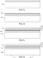
- the figures 7a to 7h illustrate an example of the manufacturing process for mirror 10.
- the method comprises in particular a step a) ( figure 7a ) which consists in providing a silicon on insulator 100 ("SOI") substrate, comprising a layer of monocrystalline silicon covering a layer of silicon dioxide formed on a substrate of monocrystalline silicon.
- SOI silicon on insulator 100
- step a) can comprise the provision of a solid substrate (for example a silicon substrate) on one face of which are formed successively, a layer of silicon dioxide and a layer of polysilicon.
- a solid substrate for example a silicon substrate
- Step a) is followed by step b) which comprises the formation of a Bragg stack 110 ( figure 7b ) on the silicon layer of the SOI substrate.
- the stack 110 notably comprises a Bragg stack.
- the Bragg stack shown in this figure comprises in particular two elementary Bragg stacks each made of a layer of silicon dioxide, 305 nm thick, and amorphous silicon, 110 nm thick.
- Step b) is followed by step c) of forming, and in order, a protective layer 130, a lower electrode 140, a PZT layer 150, and an electrode upper 160 ( figure 7c ).
- a step d) of forming a hard mask 170 (“hard mask” according to Anglo-Saxon terminology) is then executed ( figure 7d ).
- This hard mask 170 which can in particular comprise silicon dioxide, is intended to allow the release of the mirror by etching from a rear face of the SOI substrate.
- Electrode patterns 180a and 180b, as well as contact points 190a, 190b, 190c and 190d are formed during a step e) illustrated in figure 7e .
- the pattern of the mirror is together defined by the production of trenches 200 by a front face, which extends into the support of the SOI substrate ( figure 7f ).
- the invention is not limited to a mirror produced according to the method described above.
Landscapes
- Physics & Mathematics (AREA)
- General Physics & Mathematics (AREA)
- Optics & Photonics (AREA)
- Engineering & Computer Science (AREA)
- Computer Networks & Wireless Communication (AREA)
- Radar, Positioning & Navigation (AREA)
- Remote Sensing (AREA)
- Optical Elements Other Than Lenses (AREA)
- Non-Portable Lighting Devices Or Systems Thereof (AREA)
Applications Claiming Priority (1)
| Application Number | Priority Date | Filing Date | Title |
|---|---|---|---|
| FR1904137A FR3095279B1 (fr) | 2019-04-18 | 2019-04-18 | Dispositif reflecteur |
Publications (2)
| Publication Number | Publication Date |
|---|---|
| EP3726268A1 true EP3726268A1 (de) | 2020-10-21 |
| EP3726268B1 EP3726268B1 (de) | 2026-03-25 |
Family
ID=67875585
Family Applications (1)
| Application Number | Title | Priority Date | Filing Date |
|---|---|---|---|
| EP20169780.2A Active EP3726268B1 (de) | 2019-04-18 | 2020-04-16 | Reflektorvorrichtung |
Country Status (3)
| Country | Link |
|---|---|
| US (1) | US11914214B2 (de) |
| EP (1) | EP3726268B1 (de) |
| FR (1) | FR3095279B1 (de) |
Cited By (3)
| Publication number | Priority date | Publication date | Assignee | Title |
|---|---|---|---|---|
| WO2022219272A1 (fr) * | 2021-04-12 | 2022-10-20 | Commissariat A L'energie Atomique Et Aux Energies Alternatives | Dispositif réflecteur destiné à émettre une pluralité de faisceaux réfléchis à partir d'un unique faisceau lumineux principal |
| EP4553561A1 (de) | 2023-11-09 | 2025-05-14 | Commissariat à l'Energie Atomique et aux Energies Alternatives | Reflektorvorrichtung mit einem detektor und verfahren dafür |
| WO2025099071A1 (fr) | 2023-11-09 | 2025-05-15 | Commissariat A L'energie Atomique Et Aux Energies Alternatives | Dispositif réflecteur comprenant un détecteur, et procédé associé |
Families Citing this family (3)
| Publication number | Priority date | Publication date | Assignee | Title |
|---|---|---|---|---|
| US11262575B2 (en) * | 2019-03-01 | 2022-03-01 | Beijing Voyager Technology Co., Ltd. | MEMS package with double-sided mirror |
| US11493609B2 (en) * | 2019-03-01 | 2022-11-08 | Beijing Voyager Technology Co., Ltd. | MEMS device with integrated mirror position sensor |
| FR3121757B1 (fr) * | 2021-04-12 | 2023-04-14 | Commissariat Energie Atomique | Scanner optique |
Citations (2)
| Publication number | Priority date | Publication date | Assignee | Title |
|---|---|---|---|---|
| US4415234A (en) * | 1981-04-02 | 1983-11-15 | Eastman Kodak Company | Passive cooling of mirrors |
| US20060033980A1 (en) * | 2004-08-12 | 2006-02-16 | Wagner William R | Light modulator assembly |
Family Cites Families (14)
| Publication number | Priority date | Publication date | Assignee | Title |
|---|---|---|---|---|
| US4656641A (en) * | 1985-02-04 | 1987-04-07 | Xerox Corporation | Laser cavity optical system for stabilizing the beam from a phase locked multi-emitter broad emitter laser |
| JPH07104203B2 (ja) * | 1987-10-01 | 1995-11-13 | 株式会社ニコン | 照明光学装置 |
| FR2665267B1 (fr) * | 1990-07-27 | 1993-07-30 | Sextant Avionique | Dispositif optique destine a l'introduction d'une image collimatee dans le champ visuel d'un observateur et permettant la vision nocturne et casque muni d'au moins un tel dispositif. |
| US6088941A (en) * | 1992-04-06 | 2000-07-18 | A.D.P. Adaptive Visual Perception Ltd. | Transparency viewing apparatus |
| US5621227A (en) * | 1995-07-18 | 1997-04-15 | Discovery Semiconductors, Inc. | Method and apparatus for monolithic optoelectronic integrated circuit using selective epitaxy |
| JP3881467B2 (ja) * | 1998-11-30 | 2007-02-14 | 日本電信電話株式会社 | 面発光レーザ |
| JP2000266945A (ja) * | 1999-01-25 | 2000-09-29 | Alcatel | 傾斜および線形チャープを有するフィルタ光導波路 |
| JP2005337715A (ja) | 2004-05-24 | 2005-12-08 | Ideal Star Inc | バンドリジェクションミラー、フィルタ分光器、及びラマン散乱スペクトル測定用フィルタ分光器 |
| WO2010066110A1 (zh) * | 2008-12-10 | 2010-06-17 | 宏瞻科技股份有限公司 | 激光投影系统 |
| US10598769B2 (en) * | 2013-05-06 | 2020-03-24 | Danmarks Tekniske Universitet | Coaxial direct-detection LIDAR-system |
| CN103672622B (zh) * | 2013-12-20 | 2017-12-22 | 康佳集团股份有限公司 | 一种基于双反射镜的背光模组 |
| US10139476B2 (en) * | 2016-01-21 | 2018-11-27 | Institut National D'optique | Rotary scanner, opto-mechanical assembly therefore, and method of modifying an elevation angle of an optical beam |
| US10215367B2 (en) * | 2016-11-09 | 2019-02-26 | Christie Digital Systems Usa, Inc. | Apparatus for wavelength conversion |
| JP7104203B2 (ja) * | 2020-10-14 | 2022-07-20 | 株式会社あかつき | ゲームシステム、プログラム及び情報処理方法 |
-
2019
- 2019-04-18 FR FR1904137A patent/FR3095279B1/fr active Active
-
2020
- 2020-04-15 US US16/848,896 patent/US11914214B2/en active Active
- 2020-04-16 EP EP20169780.2A patent/EP3726268B1/de active Active
Patent Citations (2)
| Publication number | Priority date | Publication date | Assignee | Title |
|---|---|---|---|---|
| US4415234A (en) * | 1981-04-02 | 1983-11-15 | Eastman Kodak Company | Passive cooling of mirrors |
| US20060033980A1 (en) * | 2004-08-12 | 2006-02-16 | Wagner William R | Light modulator assembly |
Non-Patent Citations (1)
| Title |
|---|
| HARALD SCHENK ET AL.: "Micro Mirrors for high-speed Laser Deflection and Patterning", PHYSICS PROCEDIA, vol. 56, 2014, pages 7 - 18, XP029053185, DOI: 10.1016/j.phpro.2014.08.090 |
Cited By (6)
| Publication number | Priority date | Publication date | Assignee | Title |
|---|---|---|---|---|
| WO2022219272A1 (fr) * | 2021-04-12 | 2022-10-20 | Commissariat A L'energie Atomique Et Aux Energies Alternatives | Dispositif réflecteur destiné à émettre une pluralité de faisceaux réfléchis à partir d'un unique faisceau lumineux principal |
| US12607846B2 (en) | 2021-04-12 | 2026-04-21 | Commissariat A L'energie Atomique Et Aux Energies Alternatives | Reflector device for emitting a plurality of reflected beams from a single main light beam |
| EP4553561A1 (de) | 2023-11-09 | 2025-05-14 | Commissariat à l'Energie Atomique et aux Energies Alternatives | Reflektorvorrichtung mit einem detektor und verfahren dafür |
| WO2025099071A1 (fr) | 2023-11-09 | 2025-05-15 | Commissariat A L'energie Atomique Et Aux Energies Alternatives | Dispositif réflecteur comprenant un détecteur, et procédé associé |
| FR3155316A1 (fr) | 2023-11-09 | 2025-05-16 | Commissariat A L'energie Atomique Et Aux Energies Alternatives | Dispositif réflecteur comprenant un détecteur, et procédé associé |
| FR3155315A1 (fr) | 2023-11-09 | 2025-05-16 | Commissariat A L'energie Atomique Et Aux Energies Alternatives | Dispositif réflecteur comprenant un détecteur, et procédé associé |
Also Published As
| Publication number | Publication date |
|---|---|
| FR3095279B1 (fr) | 2021-05-21 |
| US20200333547A1 (en) | 2020-10-22 |
| EP3726268B1 (de) | 2026-03-25 |
| US11914214B2 (en) | 2024-02-27 |
| FR3095279A1 (fr) | 2020-10-23 |
Similar Documents
| Publication | Publication Date | Title |
|---|---|---|
| EP3726268B1 (de) | Reflektorvorrichtung | |
| EP1800188B1 (de) | Vorrichtung zur erzeugung von extremem uv-licht und anwendung auf eine lithografiequelle mit extremer uv-strahlung | |
| EP3208601B1 (de) | Nicht-dispersiver infrarotsensor zur detektion eines gases | |
| EP2466283A1 (de) | Infrarotdetektor auf der Basis von hängenden bolometrischen Mikroplatten | |
| FR3022689A1 (fr) | Module emetteur de lumiere | |
| EP4165449B1 (de) | Reflektierende optik mit einem kühlsystem | |
| FR2765411A1 (fr) | Dispositif laser solide a excitation par semi-conducteurs | |
| EP4413741A1 (de) | Infrarot-bildgebungsvorrichtung | |
| EP4406221A1 (de) | Infrarot-bildgebungsvorrichtung | |
| EP4075182B1 (de) | Optischer scanner | |
| FR3038738A1 (fr) | Dispositif optique comportant au moins un convertisseur de longueur d’onde, module lumineux et dispositif d’eclairage pour vehicule automobile comportant un tel dispositif | |
| FR3105452A1 (fr) | Dispositif de génération d’image et afficheur tête haute comprenant un tel dispositif | |
| WO2026003184A1 (fr) | Dispositif lumineux de projection pour véhicule automobile | |
| FR2979436A1 (fr) | Dispositif reflecteur pour face arriere de dispositifs optiques | |
| EP3005498B1 (de) | Laserverstärkungssystem für dicke platten und verwendungen davon | |
| FR2786035A1 (fr) | Laser solide a cavite monolythique | |
| FR3074972A1 (fr) | Element d'un laser a disque comportant le milieu amplificateur et des moyens ameliores de refroidissement. | |
| FR3158778A1 (fr) | Moyen d’émission lumineuse par conversion de longueur d’onde | |
| EP4553561A1 (de) | Reflektorvorrichtung mit einem detektor und verfahren dafür | |
| FR3063396A1 (fr) | Dispositif de signalisation pour vehicule automobile, et feu de signalisation muni d'un tel dispositif | |
| WO2022219272A1 (fr) | Dispositif réflecteur destiné à émettre une pluralité de faisceaux réfléchis à partir d'un unique faisceau lumineux principal | |
| EP1317033B1 (de) | Verstärkung eines Laserstrahls durch Pumpen eines nicht-linearen Mediums und Laservorrichtung mit solchem Verstärker | |
| FR2956748A1 (fr) | Composant optique de protection au rayonnement thermique | |
| EP4553465A1 (de) | Breitbandiger thermischer detektor mit mehreren viertelwellen-kavitäten | |
| WO2025027191A1 (fr) | Dispositif lumineux pour projeter une image sur une surface de projection située à l'intérieur d'un habitacle de véhicule automobile |
Legal Events
| Date | Code | Title | Description |
|---|---|---|---|
| PUAI | Public reference made under article 153(3) epc to a published international application that has entered the european phase |
Free format text: ORIGINAL CODE: 0009012 |
|
| STAA | Information on the status of an ep patent application or granted ep patent |
Free format text: STATUS: REQUEST FOR EXAMINATION WAS MADE |
|
| 17P | Request for examination filed |
Effective date: 20200416 |
|
| AK | Designated contracting states |
Kind code of ref document: A1 Designated state(s): AL AT BE BG CH CY CZ DE DK EE ES FI FR GB GR HR HU IE IS IT LI LT LU LV MC MK MT NL NO PL PT RO RS SE SI SK SM TR |
|
| AX | Request for extension of the european patent |
Extension state: BA ME |
|
| STAA | Information on the status of an ep patent application or granted ep patent |
Free format text: STATUS: EXAMINATION IS IN PROGRESS |
|
| RIC1 | Information provided on ipc code assigned before grant |
Ipc: G02B 5/02 20060101ALI20220531BHEP Ipc: G01S 17/00 20200101ALI20220531BHEP Ipc: B81B 3/00 20060101ALI20220531BHEP Ipc: G02B 26/08 20060101ALI20220531BHEP Ipc: G02B 7/00 20060101AFI20220531BHEP |
|
| 17Q | First examination report despatched |
Effective date: 20220628 |
|
| RAP3 | Party data changed (applicant data changed or rights of an application transferred) |
Owner name: COMMISSARIAT A L'ENERGIE ATOMIQUE ET AUX ENERGIESALTERNATIVES |
|
| GRAP | Despatch of communication of intention to grant a patent |
Free format text: ORIGINAL CODE: EPIDOSNIGR1 |
|
| STAA | Information on the status of an ep patent application or granted ep patent |
Free format text: STATUS: GRANT OF PATENT IS INTENDED |
|
| INTG | Intention to grant announced |
Effective date: 20251014 |
|
| GRAS | Grant fee paid |
Free format text: ORIGINAL CODE: EPIDOSNIGR3 |
|
| GRAA | (expected) grant |
Free format text: ORIGINAL CODE: 0009210 |
|
| STAA | Information on the status of an ep patent application or granted ep patent |
Free format text: STATUS: THE PATENT HAS BEEN GRANTED |
|
| AK | Designated contracting states |
Kind code of ref document: B1 Designated state(s): AL AT BE BG CH CY CZ DE DK EE ES FI FR GB GR HR HU IE IS IT LI LT LU LV MC MK MT NL NO PL PT RO RS SE SI SK SM TR |
|
| REG | Reference to a national code |
Ref country code: CH Ref legal event code: F10 Free format text: ST27 STATUS EVENT CODE: U-0-0-F10-F00 (AS PROVIDED BY THE NATIONAL OFFICE) Effective date: 20260325 Ref country code: GB Ref legal event code: FG4D Free format text: NOT ENGLISH |
|
| REG | Reference to a national code |
Ref country code: DE Ref legal event code: R096 Ref document number: 602020069077 Country of ref document: DE |
|
| REG | Reference to a national code |
Ref country code: IE Ref legal event code: FG4D Free format text: LANGUAGE OF EP DOCUMENT: FRENCH |