EP3726285B1 - Elektronische vorrichtung und anzeigeanordnung und rückbeleuchtungsmodul dafür - Google Patents
Elektronische vorrichtung und anzeigeanordnung und rückbeleuchtungsmodul dafür Download PDFInfo
- Publication number
- EP3726285B1 EP3726285B1 EP19748254.0A EP19748254A EP3726285B1 EP 3726285 B1 EP3726285 B1 EP 3726285B1 EP 19748254 A EP19748254 A EP 19748254A EP 3726285 B1 EP3726285 B1 EP 3726285B1
- Authority
- EP
- European Patent Office
- Prior art keywords
- light
- guide plate
- backlight module
- shielding
- light guide
- Prior art date
- Legal status (The legal status is an assumption and is not a legal conclusion. Google has not performed a legal analysis and makes no representation as to the accuracy of the status listed.)
- Active
Links
Images



Classifications
-
- G—PHYSICS
- G02—OPTICS
- G02B—OPTICAL ELEMENTS, SYSTEMS OR APPARATUS
- G02B6/00—Light guides; Structural details of arrangements comprising light guides and other optical elements, e.g. couplings
- G02B6/0001—Light guides; Structural details of arrangements comprising light guides and other optical elements, e.g. couplings specially adapted for lighting devices or systems
- G02B6/0011—Light guides; Structural details of arrangements comprising light guides and other optical elements, e.g. couplings specially adapted for lighting devices or systems the light guides being planar or of plate-like form
- G02B6/0081—Mechanical or electrical aspects of the light guide and light source in the lighting device peculiar to the adaptation to planar light guides, e.g. concerning packaging
- G02B6/0086—Positioning aspects
- G02B6/0088—Positioning aspects of the light guide or other optical sheets in the package
-
- G—PHYSICS
- G02—OPTICS
- G02F—OPTICAL DEVICES OR ARRANGEMENTS FOR THE CONTROL OF LIGHT BY MODIFICATION OF THE OPTICAL PROPERTIES OF THE MEDIA OF THE ELEMENTS INVOLVED THEREIN; NON-LINEAR OPTICS; FREQUENCY-CHANGING OF LIGHT; OPTICAL LOGIC ELEMENTS; OPTICAL ANALOGUE/DIGITAL CONVERTERS
- G02F1/00—Devices or arrangements for the control of the intensity, colour, phase, polarisation or direction of light arriving from an independent light source, e.g. switching, gating or modulating; Non-linear optics
- G02F1/01—Devices or arrangements for the control of the intensity, colour, phase, polarisation or direction of light arriving from an independent light source, e.g. switching, gating or modulating; Non-linear optics for the control of the intensity, phase, polarisation or colour
- G02F1/13—Devices or arrangements for the control of the intensity, colour, phase, polarisation or direction of light arriving from an independent light source, e.g. switching, gating or modulating; Non-linear optics for the control of the intensity, phase, polarisation or colour based on liquid crystals, e.g. single liquid crystal display cells
- G02F1/133—Constructional arrangements; Operation of liquid crystal cells; Circuit arrangements
- G02F1/1333—Constructional arrangements; Manufacturing methods
- G02F1/1335—Structural association of cells with optical devices, e.g. polarisers or reflectors
- G02F1/1336—Illuminating devices
- G02F1/133615—Edge-illuminating devices, i.e. illuminating from the side
-
- G—PHYSICS
- G02—OPTICS
- G02B—OPTICAL ELEMENTS, SYSTEMS OR APPARATUS
- G02B6/00—Light guides; Structural details of arrangements comprising light guides and other optical elements, e.g. couplings
- G02B6/0001—Light guides; Structural details of arrangements comprising light guides and other optical elements, e.g. couplings specially adapted for lighting devices or systems
- G02B6/0011—Light guides; Structural details of arrangements comprising light guides and other optical elements, e.g. couplings specially adapted for lighting devices or systems the light guides being planar or of plate-like form
- G02B6/0033—Means for improving the coupling-out of light from the light guide
- G02B6/005—Means for improving the coupling-out of light from the light guide provided by one optical element, or plurality thereof, placed on the light output side of the light guide
-
- G—PHYSICS
- G02—OPTICS
- G02B—OPTICAL ELEMENTS, SYSTEMS OR APPARATUS
- G02B6/00—Light guides; Structural details of arrangements comprising light guides and other optical elements, e.g. couplings
- G02B6/0001—Light guides; Structural details of arrangements comprising light guides and other optical elements, e.g. couplings specially adapted for lighting devices or systems
- G02B6/0011—Light guides; Structural details of arrangements comprising light guides and other optical elements, e.g. couplings specially adapted for lighting devices or systems the light guides being planar or of plate-like form
- G02B6/0033—Means for improving the coupling-out of light from the light guide
- G02B6/005—Means for improving the coupling-out of light from the light guide provided by one optical element, or plurality thereof, placed on the light output side of the light guide
- G02B6/0053—Prismatic sheet or layer; Brightness enhancement element, sheet or layer
-
- G—PHYSICS
- G02—OPTICS
- G02B—OPTICAL ELEMENTS, SYSTEMS OR APPARATUS
- G02B6/00—Light guides; Structural details of arrangements comprising light guides and other optical elements, e.g. couplings
- G02B6/0001—Light guides; Structural details of arrangements comprising light guides and other optical elements, e.g. couplings specially adapted for lighting devices or systems
- G02B6/0011—Light guides; Structural details of arrangements comprising light guides and other optical elements, e.g. couplings specially adapted for lighting devices or systems the light guides being planar or of plate-like form
- G02B6/0066—Light guides; Structural details of arrangements comprising light guides and other optical elements, e.g. couplings specially adapted for lighting devices or systems the light guides being planar or of plate-like form characterised by the light source being coupled to the light guide
- G02B6/0068—Arrangements of plural sources, e.g. multi-colour light sources
-
- G—PHYSICS
- G02—OPTICS
- G02B—OPTICAL ELEMENTS, SYSTEMS OR APPARATUS
- G02B6/00—Light guides; Structural details of arrangements comprising light guides and other optical elements, e.g. couplings
- G02B6/0001—Light guides; Structural details of arrangements comprising light guides and other optical elements, e.g. couplings specially adapted for lighting devices or systems
- G02B6/0011—Light guides; Structural details of arrangements comprising light guides and other optical elements, e.g. couplings specially adapted for lighting devices or systems the light guides being planar or of plate-like form
- G02B6/0081—Mechanical or electrical aspects of the light guide and light source in the lighting device peculiar to the adaptation to planar light guides, e.g. concerning packaging
- G02B6/0083—Details of electrical connections of light sources to drivers, circuit boards, or the like
-
- G—PHYSICS
- G02—OPTICS
- G02B—OPTICAL ELEMENTS, SYSTEMS OR APPARATUS
- G02B6/00—Light guides; Structural details of arrangements comprising light guides and other optical elements, e.g. couplings
- G02B6/0001—Light guides; Structural details of arrangements comprising light guides and other optical elements, e.g. couplings specially adapted for lighting devices or systems
- G02B6/0011—Light guides; Structural details of arrangements comprising light guides and other optical elements, e.g. couplings specially adapted for lighting devices or systems the light guides being planar or of plate-like form
- G02B6/0081—Mechanical or electrical aspects of the light guide and light source in the lighting device peculiar to the adaptation to planar light guides, e.g. concerning packaging
- G02B6/0086—Positioning aspects
- G02B6/009—Positioning aspects of the light source in the package
-
- G—PHYSICS
- G02—OPTICS
- G02B—OPTICAL ELEMENTS, SYSTEMS OR APPARATUS
- G02B6/00—Light guides; Structural details of arrangements comprising light guides and other optical elements, e.g. couplings
- G02B6/0001—Light guides; Structural details of arrangements comprising light guides and other optical elements, e.g. couplings specially adapted for lighting devices or systems
- G02B6/0011—Light guides; Structural details of arrangements comprising light guides and other optical elements, e.g. couplings specially adapted for lighting devices or systems the light guides being planar or of plate-like form
- G02B6/0081—Mechanical or electrical aspects of the light guide and light source in the lighting device peculiar to the adaptation to planar light guides, e.g. concerning packaging
- G02B6/0086—Positioning aspects
- G02B6/0091—Positioning aspects of the light source relative to the light guide
-
- G—PHYSICS
- G02—OPTICS
- G02F—OPTICAL DEVICES OR ARRANGEMENTS FOR THE CONTROL OF LIGHT BY MODIFICATION OF THE OPTICAL PROPERTIES OF THE MEDIA OF THE ELEMENTS INVOLVED THEREIN; NON-LINEAR OPTICS; FREQUENCY-CHANGING OF LIGHT; OPTICAL LOGIC ELEMENTS; OPTICAL ANALOGUE/DIGITAL CONVERTERS
- G02F1/00—Devices or arrangements for the control of the intensity, colour, phase, polarisation or direction of light arriving from an independent light source, e.g. switching, gating or modulating; Non-linear optics
- G02F1/01—Devices or arrangements for the control of the intensity, colour, phase, polarisation or direction of light arriving from an independent light source, e.g. switching, gating or modulating; Non-linear optics for the control of the intensity, phase, polarisation or colour
- G02F1/13—Devices or arrangements for the control of the intensity, colour, phase, polarisation or direction of light arriving from an independent light source, e.g. switching, gating or modulating; Non-linear optics for the control of the intensity, phase, polarisation or colour based on liquid crystals, e.g. single liquid crystal display cells
- G02F1/133—Constructional arrangements; Operation of liquid crystal cells; Circuit arrangements
- G02F1/1333—Constructional arrangements; Manufacturing methods
- G02F1/1335—Structural association of cells with optical devices, e.g. polarisers or reflectors
- G02F1/133509—Filters, e.g. light shielding masks
- G02F1/133512—Light shielding layers, e.g. black matrix
Definitions
- the present disclosure relates to the field of backlight technology of electronic devices, and in particular to an electronic device, a display assembly of an electronic device, and a backlight module of an electronic device.
- a backlight module is a significant component of an electronic device.
- the backlight module of a portable electronic device such as a mobile phone
- the light source of the edge -type backlight module and some structures related to such the light source may be required to be arranged at the side edge of the light guide plate, and therefore, a relatively large portion of a non-display region may be occupied, and an electronic device having a narrow edge and a full screen may not be easily achieved.
- US 2015/241618 A1 discloses a backlight assembly capable of preventing light leakage and a liquid crystal display (LCD) device including the same are provided.
- the backlight assembly includes a light source unit, a light guide plate, a light conversion sheet, and a reflective tape.
- the light source unit including one or more light emitting diodes (LEDs) mounted on a flexible printed circuit board (FPCB).
- the light guide plate is disposed to be adjacent to the light source unit.
- the light conversion sheet is disposed on the light guide plate and spaced apart from the FPCB, and configured to convert a wavelength band of light provided through the light guide plate from the light source unit, the light conversion sheet configured to emit white light.
- the reflective tape is attached to extend from a portion of an upper surface of the FPCB to a portion of an upper surface of the light conversion sheet.
- KR 2013 0015792 A discloses an FPCB and an LCD device to increase the thickness of an extension unit in the FPCB by forming a rebar layer on the FPCB.
- a plurality of LEDs is mounted in a mounting portion.
- An extension portion is extended from the mounting portion.
- the extension portion covers a part of a light guide plate.
- a plurality of optical sheets is arranged on the light guide plate.
- KR 2011 0041825 A discloses a backlight unit and of a liquid crystal display device to embody a uniform brightness.
- a backlight unit comprises a plurality of light emitting diodes, a light guiding plate arranged parallel with the light emitting diodes, and a light compensating part which is placed on the upper part of the light guide plate.
- the light compensating part has alternate white and black zones. The black zone faces the light emitting diodes.
- a backlight module as set out in appended claims 1 to 7 is provided.
- a display assembly as set out in appended claim 8 is provided.
- an electronic device as set out in appended claim 9 is provided.
- a backlight module includes: a light guide plate, a plurality of light sources, a light homogenizer, a flexible circuit board, and a light-shielding layer.
- the plurality of light sources are arranged on a side edge of the light guide plate and spaced apart from each other along a width direction of the light guide plate.
- the light homogenizer is arranged on the light guide plate, covering a part of a top surface of the light guide plate.
- the flexible circuit board is partially arranged on a region of the top surface of the light homogenizer uncovered by the light homogenizer, and a reservation gap is defined between the flexible circuit board and the light homogenizer.
- the light-shielding layer is arranged in a non-display region of the backlight module and is arranged to shield light emitted by the light sources and escaping from the reservation gap.
- the light-shielding layer includes a plurality of first light-shielding portions and a plurality of second light-shielding portions.
- the first light-shielding portions are arranged on regions corresponding to the light sources, and the second light-shielding portions are arranged on regions corresponding to gaps defined between every two adjacent light sources.
- a thickness of the first light-shielding portions is greater than that of the second light-shielding portions.
- a width of the non-display region of the backlight module may be reduced, and at the same time, the light may not escape out of the backlight module. Further, as the thickness of regions of the light-shielding layer corresponding to the light sources may be greater than that of regions corresponding to the gaps between light sources, uneven brightness may be prevented.
- a backlight module includes: a light guide plate; a plurality of light sources; a light homogenizer; a flexible circuit board; and a light-shielding layer.
- the plurality of light sources are arranged on a side edge of the light guide plate and spaced apart from each other along a width direction of the light guide plate, and a plurality of gaps are defined between every two adjacent light sources.
- the light homogenizer is arranged on the light guide plate, covering a region of a top surface of the light guide plate.
- the flexible circuit board is partially arranged on a region of the top surface of the light guide plate uncovered by the light homogenizer, and a reservation gap is defined between the flexible circuit board and the light homogenizer.
- the light-shielding layer is arranged in a non-display region of the backlight module and configured to shield light emitted by the plurality of light sources and escaping from the reservation gap.
- the light-shielding layer includes a plurality of first light-shielding portions and a plurality of second light-shielding portions, the plurality of first light-shielding portions are arranged to correspond to the plurality of light sources, the plurality of second light-shielding portions are arranged to correspond to the plurality of gaps, and a thickness of the plurality of first light-shielding portions is greater than a thickness of the plurality of second light-shielding portions.
- the light guide plate includes a light-incidence portion and a body portion, the plurality of light sources are arranged on a side of the light-incidence portion opposing to the body portion, and the light homogenizer is arranged on the body portion.
- the light-shielding layer is arranged between the light homogenizer and the light guide plate.
- the light homogenizer includes a diffusion film, a first brightness enhancement film, and a second brightness enhancement film, sequentially arranged along a direction away from the light guide plate, the light-shielding layer is arranged between the diffusion film and the first brightness enhancement film or between the first brightness enhancement film and the second brightness enhancement film.
- the thickness of the plurality of first light-shielding portions gradually decreases along a direction perpendicular to the side edge of the light guide plate.
- the backlight module further includes a light-shielding tape, arranged on a face of the flexible circuit board away from the plurality of light sources, and the light-shielding tape is connected to the light homogenizer.
- the backlight module further includes a connection tape.
- a portion of the flexible circuit board is connected to the region of the top surface of the light guide plate uncovered by the light homogenizer via the connection tape, and the thickness of the plurality of first light-shielding portions is less than a thickness of the connection tape.
- a display assembly includes a display panel and a backlight module providing backlight for the display panel.
- the backlight module includes: a light guide plate; a plurality of light sources; a light homogenizer; a flexible circuit board; and a light-shielding layer.
- the plurality of light sources are arranged on a side edge of the light guide plate and spaced apart from each other along a width direction of the light guide plate, and a plurality of gaps are defined between every two adjacent light sources.
- the light homogenizer is arranged on the light guide plate, covering a region of a top surface of the light guide plate.
- the flexible circuit board is partially arranged on a region of the top surface of the light guide plate uncovered by the light homogenizer, and a reservation gap is defined between the flexible circuit board and the light homogenizer.
- the light-shielding layer is arranged in a non-display region of the backlight module and configured to shield light emitted by the plurality of light sources and escaping from the reservation gap.
- the light-shielding layer includes a plurality of first light-shielding portions and a plurality of second light-shielding portions, the plurality of first light-shielding portions are arranged to correspond to the plurality of light sources, the plurality of second light-shielding portions are arranged to correspond to the plurality of gaps, and a thickness of the plurality of first light-shielding portions is greater than a thickness of the plurality of second light-shielding portions. The thickness of the plurality of first light-shielding portions is gradually decreased along a direction away from the plurality of light sources.
- the light guide plate includes a light-incidence portion and a body portion, the plurality of light sources are arranged on a side of the light-incidence portion opposing to the body portion, and the light homogenizer is arranged on the body portion.
- the light homogenizer includes a diffusion film, a first brightness enhancement film, and a second brightness enhancement film, sequentially arranged along a direction away from the light guide plate, and the light-shielding layer is arranged between the diffusion film and the first brightness enhancement film or between the first brightness enhancement film and the second brightness enhancement film.
- the backlight module further includes a light-shielding tape, arranged on a face of the flexible circuit board away from the plurality of light sources, and the light-shielding tape is connected to the light homogenizer.
- an electronic device includes a back shell, a middle frame, and a display assembly.
- the middle frame is fixedly connected to the back shell.
- the display assembly is fixed with the middle frame.
- the display assembly includes a display panel and the backlight module as described in the first aspect of the present disclosure.
- FIG. 1 is a top view of a light guide plate exhibiting a positional relation among the light guide plate, a light-shielding layer, and a light source according to an embodiment of the present disclosure
- FIG. 2 is a cross-sectional view of the backlight module according to the embodiment shown in FIG. 1 , taken along a line II-II
- FIG. 3 is a cross-sectional view of the backlight module according to the embodiment shown in FIG. 1 , taken along a line III-III.
- the backlight module may include a back frame 11, a reflection sheet 12, a light guide plate 13, a light homogenizer 14, a light-shielding layer 15, a flexible circuit board 16, a connection tape 17, a light-shielding tape 18, a first glue frame 19, a second glue frame 20, and a plurality of light sources 21.
- the back frame 11 has a boxed structure and defines an opening on a side of the back frame 11.
- the back frame 11 may include a bottom wall 111 and a side wall 112.
- the bottom wall 111 and the side wall 112 are bent to connect to each other.
- the bottom wall 111 and the side wall 112 define a receiving chamber.
- the back frame 11 may be made of metal, such as iron, aluminum, and the like.
- the reflection sheet 12 may be arranged on the bottom wall 111 of the back frame 11 and received in the receiving chamber.
- the light guide plate 13 may be arranged on the reflection sheet 12, covering a region of a top surface of the reflection sheet 12, and received in the receiving chamber.
- the light guide plate 13 may include a light-incidence portion 131 and a body portion 132.
- the light-incidence portion 131 may have a light-incidence side, and a thickness of the light-incidence portion 131may be greater than a thickness of the body portion 132
- a thickness of the light-incidence portion 131 may be gradually decreased from the light-incidence side to a side away from the light-incidence side.
- the thickness of the body portion 132 of the light guide plate may be uniform, and that is each region of the body portion 132 may have a same thickness.
- the plurality of light sources 21 may be arranged on a region of the top surface of the reflection sheet 12 uncovered by the light guide plate 13 and on a side edge of the light guide plate 13.
- the plurality of light sources 21 are arranged on the light-incidence side of the light guide plate 13.
- the plurality of light sources 21 may be a plurality of light-emitting diode (LED) lamps.
- the plurality of light sources 21 may be arranged on a side of the light-incidence portion 131 opposing to the body portion 132 of the light guide plate. For example, as shown in FIG. 2 , the plurality of light sources 21 may be arranged on a left side of the light guide plate 13.
- the light guide plate may be rectangular from the top view, and the plurality of light sources 21 are spaced apart from each other along a width direction of the light guide plate 13.
- the light homogenizer 14 is arranged on the body portion 132 of the light guide plate, covering a portion of the light guide plate 13.
- the light homogenizer 14 may include a diffusion film 141, a first brightness enhancement film 142, and a second brightness enhancement film 142, sequentially arranged along a direction away from the light guide plate 13.
- the diffusion film 141, the first brightness enhancement film 142, and the second brightness enhancement film 143 may be independent from each other.
- at least two of the diffusion film 141, the first brightness enhancement film 142, and the second brightness enhancement film 143 may be arranged as one integrated structure.
- the first glue frame 19 may be arranged on the bottom wall 111 of the back frame 11 and may abut against the side wall 112.
- the first glue frame 19 may be arranged on a side of each light source 21 away from the light guide plate 13.
- the first glue frame 19 may be arranged on a left side of the plurality of light sources 21 as shown in FIG. 2 , and a space may be defined between the first glue frame 19 and the plurality of light sources 21 for light mixing and heat dissipation.
- the flexible circuit board 16 is partially arranged on a portion of the light guide plate 13 uncovered by the light homogenizer 14, and a portion of the flexible circuit board 16 that is not arranged on the light guide plate 13 may be arranged above the first glue frame 19 and the plurality of light sources 21.
- the plurality of light sources 21 may be fixed on a bottom surface of the portion of the flexible circuit board 16 that is not arranged on the light guide plate 13.
- the plurality of light sources 21 may be electrically connected to the flexible circuit board 16.
- a line on the flexible circuit board 16 may connect to the plurality of light sources 21 and an external power supply pin, such that the external power supply pin 21 may provide power for the plurality of light sources 21.
- the flexible circuit board 16 may be adhered to the portion of the light guide plate 13 uncovered by the light homogenizer 14 via the connection tape 17.
- the connection tape 17 may be a double-sided tape. A side of the double-sided tape may be adhered to the bottom surface of the flexible circuit board 17, and the other side of the double-sided tape may be adhered to a top surface of the light guide plate 13 correspondingly.
- a reservation gap 190 is defined between an end of the flexible circuit board 16 and the connection tape 17 close to the light homogenizer 14 and an end of the light homogenizer 14 close to the flexible circuit board 16.
- the reservation gap 190 may be defined to allow an assembling error and allow the backlight module to work normally when deformation caused by high and low temperatures occurs.
- the light-shielding tape 18 may be arranged on the flexible circuit board 16 and a portion of the light homogenizer 14.
- the light-shielding tape 18 may be adhered to a top surface of the light homogenizer 14, such that the light homogenizer 14 may be fixed.
- the light-shielding tape 18 may include a first sub-light-shielding portion 181 and a second sub-light-shielding portion 182.
- the first sub-light-shielding tape 181 may be arranged to cover the flexible circuit board 16, and the second sub-light-shielding portion 182 may be arranged to cover a portion of the light homogenizer 14.
- a thickness of the first sub-light-shielding portion 181 may be greater than that of the second sub-light-shielding portion 182.
- the second glue frame 20 may be arranged on a side of the light-shielding tape 18 and the flexible circuit board 16 away from the light homogenizer 14 (such as a left side shown in FIG. 2 ) to fix the light-shielding tape 18 and the flexible circuit board 16.
- the first glue frame 19 may be received in the receiving chamber of the back frame 11, and the second glue frame 20 may be arranged out of the receiving chamber of the back frame 11.
- the light-shielding layer 15 is arranged in a non-display region of the backlight module and is configured to shield the light emitted by the plurality of light sources 21 and escaping from the reservation gap 190, such that the light emitted by the plurality of light sources 21 and escaping from the reservation gap 190 is shielded by the light-shielding layer 15.
- the non-display region may refer to a region covered by the light-shielding tape 18, and a display region may refer to a region uncovered by the light-shielding tape 18.
- the light shielding layer 15 may be arranged between the light homogenizer 14 and the light guide plate 13.
- a region covered by the light-shielding layer 15 may correspond to an end region of an end of the light homogenizer 14 close to the plurality of light sources 21.
- the light-shielding layer 15 may be arranged on a surface of the light homogenizer 14 close to the light guide plate 13 or a surface of the light guide plate 13 close to the light homogenizer 14.
- the light-shielding layer 15 may be arranged at any position within the non-display region, with the proviso of the light emitted by the plurality of light sources 31 able to be blocked from escaping from the reservation gap 190.
- the light-shielding layer 15 may be arranged between the diffusion film 141 and the first brightness enhancement film 142. Specifically, the light-shielding layer 15 may be arranged on a surface of the diffusion film 141 close to the first brightness enhancement film 142. Alternatively, the light-shielding layer 15 may be arranged on a surface of the first brightness enhancement film 142 close to the diffusion film 141. A region covered by the light-shielding layer correspond to an end region of an end of the diffusion film 141 close to the plurality of light sources 21 or an end region of an end of the first brightness enhancement film 142 close to the plurality of light sources 21.
- the light-shielding layer 15 may be made of light-shielding material.
- the light-shielding layer 15 may be a layer of black ink.
- the light shielding layer 15 may be formed by performing a printing process or a coating process.
- the printing process may be a screen printing process.
- the light-shielding layer 15 includes a plurality of first light-shielding portions 151 and a plurality of second light-shielding portions 152.
- the plurality of first light-shielding portions 151 are arranged on regions corresponding to the plurality of light sources 21.
- the plurality of second light-shielding portions 152 are arranged on regions corresponding to a plurality of gaps, and each gap is defined between two adjacent light sources 21.
- a number of the printing or the coating process performed to form the plurality of first light-shielding portions 151 may be greater than that performed to form the plurality of second light-shielding portions 152, such that a thickness of the plurality of first light-shielding portions 151 may be greater than that of the second light-shielding portions 152.
- the plurality of first light-shielding portions 151 may be formed on the surface of the light guide plate 13 by performing the printing processes twice.
- the plurality of second light-shielding portions 152 may be formed on the surface of the light guide plate 13 by perform the printing process once. A different number of times performing the printing process may be applied herein, and is not limited by the present disclosure.
- the thickness of the plurality of first light-shielding portions 151 may be less than that of the connection tape 17.
- the thickness of the light-shielding layer 15 on the regions corresponding to the plurality of light sources 21 is greater than that of the light-shielding layer 15 on regions corresponding to the gaps between every two adjacent light sources 21 (i.e., the second light-shielding portions 152).
- a region in which the plurality of light sources21 is located may have higher brightness, and a gap between two adjacent light sources may have lower brightness, such arrangement of the light-shielding layer 15 may prevent unequal brightness of the region in which a light source 21 is located and the gap between two adjacent light sources.
- FIG. 2 is a cross-sectional view of the region corresponding to the light source, and therefore, the light-shielding layer 15 shown in FIG. 2 may be a first light-shielding portion 151.
- FIG. 3 is a cross-sectional view of the region corresponding to the gap between two adjacent light sources, and therefore, the light-shielding layer 15 shown in FIG. 3 may be a second light-shielding portion 152.
- the light-shielding layer 15 may be formed by performing a photolithographic process or an etching process.
- a degree of the photolithographic process or the etching process to form the plurality of first light-shielding portions 151 may be less than that to form the plurality of second light-shielding portions 152, such that the thickness of the plurality of first light-shielding portions 151 may be greater than that of the second light-shielding portions 152.
- a light-shielding substrate having a uniform thickness may be formed on the top surface of the light guide plate 13 firstly. Subsequently, a mask may be disposed on the light-shielding substrate to shield regions of the light-shielding substrate corresponding to the plurality of light sources 21, and regions of the light-shielding substrate corresponding to the gaps between every two adjacent light sources 21may be exposed through a plurality of openings of the mask.
- the photolithographic process may be performed on the exposed regions of the light-shielding substrate, such that the second light-shielding portions 152 having a relatively small thickness may be formed in the exposed regions, and the first light-shielding portions 151 having a relatively large thickness may be formed in the regions covered by the mask. Under such situation, the degree of the photolithographic process to form the first light-shielding portions 151 may be zero, and the degree of the photolithographic process to form the second light-shielding portions152 may be greater than zero.
- a light-shielding substrate having a uniform thickness may be formed on the top surface of the light guide plate 13.
- a semi-transparent mask may be disposed on the light-shielding substrate.
- the semi-transparent mask may include a plurality of first regions and a plurality of second regions. A transparency of the first regions may be less than that of the second regions.
- the first regions may be arranged above regions of the light-shielding substrate corresponding to the plurality of light sources 13, and the second regions may be arranged above regions of the light-shielding substrate corresponding to gaps between every two adjacent light sources.
- Light with a same parameter may irradiate the semi-transparent mask, such that the plurality of first light-shielding portions 151 having a relatively large thickness may be formed in regions of the light-shielding substrate covered by the plurality of first regions, and the plurality of second light-shielding portions 152 having a relatively small thickness may be formed in regions of the light-shielding substrate covered by the plurality of second regions.
- intensity of light for photolithographing to form the plurality of first light-shielding portions 151 may be less than that to form the plurality of second light-shielding portions 152, and various degrees of the photolithographic process may be achieved.
- the various degrees of the photolithographic process may be achieved by applying various durations of the photolithographic process.
- a duration of the photolithographic process to form the plurality of first light-shielding portions 151 may be less than a duration of the photolithographic process to form the plurality of second light-shielding portions 152, such that the various degrees of the photolithographic process may be achieved.
- the plurality of first light-shielding portions 151 and the plurality of second light-shielding portions 152 may be formed by performing the etching process.
- a degree of the etching process to form the plurality of first light-shielding portions 151 may be less than that to form the plurality of second light-shielding portions 152.
- various degrees of the etching process may be achieved by applying various values of etching parameters, such as various durations of the etching process, various concentrations of an etching solution, and the like.
- the duration of the etching process performed to form the first light-shielding portions 151 may be less than that to form the second light-shielding portions 152, and/or the concentration of the etching solution to form the first light-shielding portions 151 may be less than that to form the second light-shielding portions 152, such that the thickness of the first light-shielding portions 151 may be greater than that of the second light-shielding portions 152.
- first light-shielding portions 151 thicker than the second light-shielding portions 152 may be achieved by other means, which will not be limited by the present disclosure.
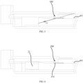
- FIG. 4 is a schematic view of the backlight module in a position shown in FIG. 2 , showing a principle of a light-shielding layer shielding light
- FIG. 5 is a schematic view of the backlight module in a position shown in FIG. 3 , showing a principle of a light-shielding layer shielding light.
- light S1 may be supposed to be emitted by light source 21, passing through and escaping from the reservation gap 190.
- the light S1 may be shielded by the light-shielding layer 15 (specifically, the first light-shielding portion 151), such that the light may not irradiate to an outside of the backlight module, and may not irradiate to a user's eyes directly.
- the light-shielding layer 15 may not occupy an independent space along a width direction. Therefore, the width of the non-display region of the backlight module may be reduced, and light escaping may be reduced.
- light S2 may be emitted by a light source 21 adjacent to the gap between two adjacent light sources 21, i.e., emitted by at least one of the two adjacent light sources 21 defining the gap. Intensity of the light S2 may be less than that of the light S1.
- the light S2 may be supposed to escape from the reservation gap 190 to irradiate to an outside of the backlight module.
- the arrangement of the light-shielding layer 15 (specifically, the second light-shielding portion 152) may shield the light S2, such that the light S2 may not irradiate to the outside of the backlight module and may not irradiate to the user's eyes.
- intensity of the light S1 irradiated from a region corresponding to the light source 21 may be greater than that of the light S2 irradiated from a region corresponding to the gap between two adjacent light sources 21, and the thickness of the first light-shielding portion 151 may be arranged to be greater than that of the second light-shielding portion 152, such that a light-shielding effect of the light-shielding layer 15 on the region corresponding to the light source 21 may be greater than that on the region corresponding to the gap between two adjacent light sources 21, such that uneven brightness across the side edge of the light guide plate 13 may be reduced.
- the thickness of the first light-shielding portion 151 may be gradually decreased along a direction away from the light source 21. As the closer to the light source 21, the higher intensity of the light, such the arrangement may prevent the light guide plate 13 from having uneven light intensities along a length direction of the light guide plate 13.
- the thickness of the first light-shielding portion 151 being greater than that of the second light-shielding portion 152 may specifically refer to a thickness of a thinnest portion of the first light-shielding portion 151 being greater than the thickness of the second light-shielding portion 152.
- the electronic device 50 may be a smart mobile phone.
- the electronic device may be a tablet computer, a handheld computer, an intelligent watch, and the like.
- the electronic device 20 may include a back shell 51, a middle frame 52, a display assembly 53, and a cover 54.
- the middle frame 52 may be fixedly connected to the back shell 51.
- the display assembly 53 may be fixed with the middle frame 52.
- the display assembly 53 may include a backlight module 531 and a display panel 532.
- the backlight module 53 may be configured to provide backlight for the display panel 532.
- the display panel 532 may be a liquid crystal display panel or a display panel in another type.
- the cover 54 may be arranged to cover the display assembly 53.
- the cover 54 may be a transparent glass cover.
- the cover 54 may be non-transparent.
- the cover 54 maybe coated by light-shielding ink for the non-display region.
- the electronic device 50 may have other structures.
- the above description about the structures of the electronic device 50 may not limit the scope of the present disclosure.
Landscapes
- Physics & Mathematics (AREA)
- General Physics & Mathematics (AREA)
- Optics & Photonics (AREA)
- Nonlinear Science (AREA)
- Mathematical Physics (AREA)
- Chemical & Material Sciences (AREA)
- Crystallography & Structural Chemistry (AREA)
- Planar Illumination Modules (AREA)
- Liquid Crystal (AREA)
Claims (9)
- Rückbeleuchtungsmodul für eine Anzeigeanordnung, wobei das Rückbeleuchtungsmodul eine Anzeigeregion zum Bereitstellen von Licht an die Anzeigeanordnung sowie eine Nicht-Anzeigeregion umfasst, die der Anzeigeanordnung kein Licht bereitstellt, wobei das Rückbeleuchtungsmodul des Weiteren umfasst:eine Lichtleiterplatte (13);eine Vielzahl von Lichtquellen (21), die auf einem Seitenrand der Lichtleiterplatte (13) angeordnet und voneinander entlang einer Breitenrichtung der Lichtleiterplatte (13) beabstandet sind, wobei zwischen jeweils zwei benachbarten Lichtquellen (21) eine Vielzahl von Lücken definiert ist;einen Lichthomogenisierer (14), der auf der Lichtleiterplatte (13) angeordnet ist und eine Region auf einer obersten Oberfläche der Lichtleiterplatte (13) bedeckt;eine flexible Schaltplatine (16), die teilweise auf einer Region der obersten Oberfläche der Lichtleiterplatte (13) angeordnet und nicht durch den Lichthomogenisierer (14) bedeckt ist, wobei eine Reservierungslücke (190) zwischen der flexiblen Schaltplatine (16) und dem Lichthomogenisierer (14) definiert ist; undeine Lichtabschirmschicht (15), die in der Nicht-Anzeigeregion des Rückbeleuchtungsmoduls angeordnet ist und ausgestaltet ist, um Licht abzuschirmen, das von der Vielzahl der Lichtquellen (21) emittiert wird und aus der Reservierungslücke (190) entweicht,wobei das Rückbeleuchtungsmodul dadurch gekennzeichnet ist, dass die Lichtabschirmschicht (15) eine Vielzahl von ersten Lichtabschirmabschnitten (151) und eine Vielzahl von zweiten Lichtabschirmabschnitten (152) umfasst, die Vielzahl der ersten Lichtabschirmabschnitte (151) in Regionen angeordnet ist, welche der Vielzahl der Lichtquellen (21) entsprechen, die Vielzahl der zweiten Lichtabschirmabschnitte (152) in Regionen angeordnet ist, die der Vielzahl der Lücken entsprechen, und wobei eine Dicke der Vielzahl der ersten Lichtabschirmabschnitte (151) größer als eine Dicke der Vielzahl der zweiten Lichtabschirmabschnitte (152) ist.
- Rückbeleuchtungsmodul nach Anspruch 1, wobei die Lichtleiterplatte (13) einen Lichteinfallabschnitt (131) und einen Körperabschnitt (132) umfasst, die Vielzahl der Lichtquellen (21) auf einer Seite des Lichteinfallabschnitts (131) gegenüber von dem Körperabschnitt (132) angeordnet ist, und der Lichthomogenisierer (14) auf dem Körperabschnitt (132) angeordnet ist.
- Rückbeleuchtungsmodul nach Anspruch 1, wobei die Lichtabschirmschicht (15) zwischen dem Lichthomogenisierer (14) und der Lichtleiterplatte (13) angeordnet ist, und eine durch die Lichtabschirmschicht bedeckte Region einem Endabschnitt des Lichthomogenisierers oder der Lichtleiterplatte nahe an der Vielzahl der Lichtquellen entspricht.
- Rückbeleuchtungsmodul nach Anspruch 1, wobei der Lichthomogenisierer (14) einen Diffusionsfilm (141), einen ersten Helligkeitsverbesserungsfilm (142) und einen zweiten Helligkeitsverbesserungsfilm (143) umfasst, die sequentiell entlang einer Richtung angeordnet sind, die von der Lichtleiterplatte (13) weg weist, wobei die Lichtabschirmschicht (15) zwischen dem Diffusionsfilm (141) und dem ersten Helligkeitsverbesserungsfilm (142) oder zwischen dem ersten Helligkeitsverbesserungsfilm (142) und dem zweiten Helligkeitsverbesserungsfilm (143) angeordnet ist.
- Rückbeleuchtungsmodul nach Anspruch 1, wobei die Dicke der Vielzahl der ersten Lichtabschirmabschnitte (151) entlang einer Richtung, die senkrecht zu dem Seitenrand der Lichtleiterplatte ist, allmählich abnimmt.
- Rückbeleuchtungsmodul nach Anspruch 1, des Weiteren umfassend ein Lichtabschirmband (18), das auf einer Seite der flexiblen Schaltplatine (16) angeordnet ist, die von der Vielzahl der Lichtquellen (21) weg weist, wobei das Lichtabschirmband (18) mit dem Lichthomogenisierer (14) verbunden ist.
- Rückbeleuchtungsmodul nach Anspruch 1, des Weiteren umfassend ein Verbindungsband (17), wobei ein Abschnitt der flexiblen Schaltplatine (16) mit der Region der obersten Oberfläche der Lichtleiterplatte (13), die nicht durch den Lichthomogenisierer (14) bedeckt ist, mittels des Verbindungsbands (17) verbunden ist, und wobei die Dicke der Vielzahl der ersten Lichtabschirmabschnitte (151) kleiner als eine Dicke des Verbindungsbands (17) ist.
- Anzeigeanordnung, umfassend ein Anzeigefeld (532) und das Rückbeleuchtungsmodul nach einem der Ansprüche 1 bis 7,
wobei das Rückbeleuchtungsmodul ausgestaltet ist, um dem Anzeigefeld (532) Rückbeleuchtung bereitzustellen. - Elektronische Vorrichtung, umfassend eine Rückenschale (51), einen Mittelrahmen (52) und eine Anzeigeanordnung (53), wobei der Mittelrahmen (52) fixiert mit der Rückenschale (51) verbunden ist, die Anzeigeanordnung (53) an dem Mittelrahmen (52) fixiert ist, die Anzeigeanordnung (53) ein Anzeigefeld (532) und das Rückbeleuchtungsmodul nach einem der Ansprüche 1 bis 7 umfasst.
Applications Claiming Priority (2)
| Application Number | Priority Date | Filing Date | Title |
|---|---|---|---|
| CN201810106074.1A CN108254973A (zh) | 2018-01-31 | 2018-01-31 | 电子装置及其显示组件、背光模组 |
| PCT/CN2019/072194 WO2019149085A1 (zh) | 2018-01-31 | 2019-01-17 | 电子装置及其显示组件、背光模组 |
Publications (3)
| Publication Number | Publication Date |
|---|---|
| EP3726285A1 EP3726285A1 (de) | 2020-10-21 |
| EP3726285A4 EP3726285A4 (de) | 2021-02-24 |
| EP3726285B1 true EP3726285B1 (de) | 2023-07-26 |
Family
ID=62743761
Family Applications (1)
| Application Number | Title | Priority Date | Filing Date |
|---|---|---|---|
| EP19748254.0A Active EP3726285B1 (de) | 2018-01-31 | 2019-01-17 | Elektronische vorrichtung und anzeigeanordnung und rückbeleuchtungsmodul dafür |
Country Status (4)
| Country | Link |
|---|---|
| US (1) | US11187850B2 (de) |
| EP (1) | EP3726285B1 (de) |
| CN (1) | CN108254973A (de) |
| WO (1) | WO2019149085A1 (de) |
Families Citing this family (8)
| Publication number | Priority date | Publication date | Assignee | Title |
|---|---|---|---|---|
| CN110095835A (zh) * | 2018-01-31 | 2019-08-06 | 广东欧珀移动通信有限公司 | 一种背光模组及电子装置 |
| CN108254973A (zh) | 2018-01-31 | 2018-07-06 | 广东欧珀移动通信有限公司 | 电子装置及其显示组件、背光模组 |
| CN113823185B (zh) * | 2020-06-19 | 2023-09-12 | 群创光电股份有限公司 | 电子装置 |
| CN111708206B (zh) * | 2020-07-17 | 2024-03-26 | 合肥鑫晟光电科技有限公司 | 一种触控显示模组及其制作方法、显示装置 |
| CN114509896B (zh) * | 2022-02-09 | 2023-10-31 | 广州华星光电半导体显示技术有限公司 | 液晶显示模组 |
| CN114879403B (zh) * | 2022-05-23 | 2023-06-27 | 业成科技(成都)有限公司 | 显示装置制造方法和显示装置 |
| CN115966647B (zh) * | 2022-12-29 | 2023-09-15 | 东莞市通豪实业投资有限公司 | 一种应用于触控总成的led显示结构及其制作方法和应用 |
| CN119376131B (zh) * | 2023-07-25 | 2026-03-27 | 北京小米移动软件有限公司 | 一种显示模组及其制备方法、电子设备 |
Family Cites Families (20)
| Publication number | Priority date | Publication date | Assignee | Title |
|---|---|---|---|---|
| JP5083111B2 (ja) * | 2008-08-07 | 2012-11-28 | オムロン株式会社 | 面光源装置 |
| EP2470952B1 (de) * | 2009-08-27 | 2016-02-10 | LG Electronics Inc. | Rückbeleuchtungseinheit und anzeigevorrichtung |
| KR20110041825A (ko) * | 2009-10-16 | 2011-04-22 | 엘지디스플레이 주식회사 | 백라이트 유닛 및 이를 구비한 액정표시장치 |
| CN102597603B (zh) * | 2009-12-28 | 2014-09-03 | 夏普株式会社 | 面状照明装置和具备它的显示装置 |
| WO2013011912A1 (ja) * | 2011-07-19 | 2013-01-24 | シャープ株式会社 | バックライトユニット及び液晶表示装置 |
| KR101791538B1 (ko) * | 2011-08-05 | 2017-10-30 | 엘지디스플레이 주식회사 | 연성회로기판 및 액정표시장치 |
| JP6092522B2 (ja) * | 2012-04-11 | 2017-03-08 | サターン ライセンシング エルエルシーSaturn Licensing LLC | 発光装置、表示装置および照明装置 |
| CN202837741U (zh) * | 2012-08-31 | 2013-03-27 | 惠州比亚迪实业有限公司 | 一种lcd模组 |
| CN103175034A (zh) * | 2013-03-26 | 2013-06-26 | 南京中电熊猫液晶显示科技有限公司 | Led背光模组 |
| CN103527966B (zh) * | 2013-10-30 | 2015-08-19 | 京东方科技集团股份有限公司 | 一种led灯条、侧光式背光源模组及显示装置 |
| KR102096436B1 (ko) * | 2014-02-27 | 2020-04-02 | 엘지디스플레이 주식회사 | 백라이트 어셈블리 및 이를 포함하는 액정표시장치 |
| CN204129371U (zh) | 2014-09-28 | 2015-01-28 | 深圳市众搏辉科技有限公司 | 防漏光的显示屏固定结构 |
| CN104536167A (zh) * | 2014-12-23 | 2015-04-22 | 深圳市华星光电技术有限公司 | 一种窄边框显示装置 |
| CN204403961U (zh) * | 2015-03-10 | 2015-06-17 | 信利半导体有限公司 | 背光源及液晶显示模组 |
| CN204719370U (zh) | 2015-06-08 | 2015-10-21 | 东莞市钰晟电子科技有限公司 | 一种新型窄边框背光源防漏光光学膜 |
| CN205427394U (zh) | 2015-12-16 | 2016-08-03 | 广东星亚星半导体股份有限公司 | 一种防漏光的液晶显示屏 |
| JP2017198735A (ja) | 2016-04-25 | 2017-11-02 | 大日本印刷株式会社 | 光学シート、映像源ユニット及び液晶表示装置 |
| CN106842713B (zh) * | 2017-04-12 | 2024-04-16 | Oppo广东移动通信有限公司 | 背光模组及电子装置 |
| CN206638920U (zh) | 2017-04-12 | 2017-11-14 | 广东欧珀移动通信有限公司 | 背光模组及电子装置 |
| CN108254973A (zh) * | 2018-01-31 | 2018-07-06 | 广东欧珀移动通信有限公司 | 电子装置及其显示组件、背光模组 |
-
2018
- 2018-01-31 CN CN201810106074.1A patent/CN108254973A/zh active Pending
-
2019
- 2019-01-17 EP EP19748254.0A patent/EP3726285B1/de active Active
- 2019-01-17 WO PCT/CN2019/072194 patent/WO2019149085A1/zh not_active Ceased
-
2020
- 2020-06-29 US US16/915,393 patent/US11187850B2/en not_active Expired - Fee Related
Also Published As
| Publication number | Publication date |
|---|---|
| WO2019149085A1 (zh) | 2019-08-08 |
| EP3726285A1 (de) | 2020-10-21 |
| CN108254973A (zh) | 2018-07-06 |
| US11187850B2 (en) | 2021-11-30 |
| US20200326469A1 (en) | 2020-10-15 |
| EP3726285A4 (de) | 2021-02-24 |
Similar Documents
| Publication | Publication Date | Title |
|---|---|---|
| EP3726285B1 (de) | Elektronische vorrichtung und anzeigeanordnung und rückbeleuchtungsmodul dafür | |
| US10180534B2 (en) | Borderless display device including display module | |
| KR100859537B1 (ko) | 면상 광원장치 | |
| EP3217250B1 (de) | Randlose anzeigevorrichtung mit anzeigemodul | |
| US8049833B2 (en) | Liquid crystal display device | |
| US20080002099A1 (en) | Multilevel tool tree | |
| US10274142B2 (en) | Lighting device and display device | |
| KR102463913B1 (ko) | 표시장치 | |
| KR102855928B1 (ko) | 백라이트 유닛 및 그를 포함하는 표시장치 | |
| KR20100082640A (ko) | 광원 유닛 및 그를 포함하는 표시 장치 | |
| WO2011093119A1 (ja) | 照明装置、表示装置、テレビ受信装置 | |
| KR20150077153A (ko) | 광원 모듈 및 이를 구비한 백라이트 유닛 | |
| US20160334560A1 (en) | Display device including accommodating member | |
| WO2017073471A1 (ja) | 照明装置及び表示装置 | |
| CN108317436B (zh) | 一种背光模组及电子装置 | |
| EP2333592A2 (de) | Rückbeleuchtungseinheit und Anzeigevorrichtung damit | |
| US10203442B2 (en) | Lighting device including a side emitting type light source for improved light efficiency and display device | |
| KR102322455B1 (ko) | 표시 장치 | |
| CN103732973A (zh) | 照明装置和具备它的显示装置 | |
| KR102253430B1 (ko) | 표시 장치 | |
| JP2005321586A (ja) | 面光源ユニット及び液晶表示装置 | |
| US9690039B2 (en) | Light source device and display device | |
| WO2017077910A1 (ja) | 照明装置及び表示装置 | |
| KR20130072971A (ko) | 백라이트 유닛 및 이를 구비한 액정표시장치 | |
| US9182536B2 (en) | Light-source device and display device |
Legal Events
| Date | Code | Title | Description |
|---|---|---|---|
| STAA | Information on the status of an ep patent application or granted ep patent |
Free format text: STATUS: THE INTERNATIONAL PUBLICATION HAS BEEN MADE |
|
| PUAI | Public reference made under article 153(3) epc to a published international application that has entered the european phase |
Free format text: ORIGINAL CODE: 0009012 |
|
| STAA | Information on the status of an ep patent application or granted ep patent |
Free format text: STATUS: REQUEST FOR EXAMINATION WAS MADE |
|
| 17P | Request for examination filed |
Effective date: 20200713 |
|
| AK | Designated contracting states |
Kind code of ref document: A1 Designated state(s): AL AT BE BG CH CY CZ DE DK EE ES FI FR GB GR HR HU IE IS IT LI LT LU LV MC MK MT NL NO PL PT RO RS SE SI SK SM TR |
|
| AX | Request for extension of the european patent |
Extension state: BA ME |
|
| A4 | Supplementary search report drawn up and despatched |
Effective date: 20210125 |
|
| RIC1 | Information provided on ipc code assigned before grant |
Ipc: G02B 6/42 20060101ALI20210119BHEP Ipc: G02F 1/13357 20060101AFI20210119BHEP Ipc: G02B 6/00 20060101ALI20210119BHEP |
|
| DAV | Request for validation of the european patent (deleted) | ||
| DAX | Request for extension of the european patent (deleted) | ||
| STAA | Information on the status of an ep patent application or granted ep patent |
Free format text: STATUS: EXAMINATION IS IN PROGRESS |
|
| 17Q | First examination report despatched |
Effective date: 20220404 |
|
| REG | Reference to a national code |
Ref country code: DE Ref legal event code: R079 Free format text: PREVIOUS MAIN CLASS: G02F0001133570 Ipc: F21V0008000000 Ref country code: DE Ref legal event code: R079 Ref document number: 602019033574 Country of ref document: DE Free format text: PREVIOUS MAIN CLASS: G02F0001133570 Ipc: F21V0008000000 |
|
| GRAP | Despatch of communication of intention to grant a patent |
Free format text: ORIGINAL CODE: EPIDOSNIGR1 |
|
| STAA | Information on the status of an ep patent application or granted ep patent |
Free format text: STATUS: GRANT OF PATENT IS INTENDED |
|
| RIC1 | Information provided on ipc code assigned before grant |
Ipc: F21V 8/00 20060101AFI20230322BHEP |
|
| INTG | Intention to grant announced |
Effective date: 20230414 |
|
| GRAS | Grant fee paid |
Free format text: ORIGINAL CODE: EPIDOSNIGR3 |
|
| GRAA | (expected) grant |
Free format text: ORIGINAL CODE: 0009210 |
|
| STAA | Information on the status of an ep patent application or granted ep patent |
Free format text: STATUS: THE PATENT HAS BEEN GRANTED |
|
| AK | Designated contracting states |
Kind code of ref document: B1 Designated state(s): AL AT BE BG CH CY CZ DE DK EE ES FI FR GB GR HR HU IE IS IT LI LT LU LV MC MK MT NL NO PL PT RO RS SE SI SK SM TR |
|
| REG | Reference to a national code |
Ref country code: CH Ref legal event code: EP |
|
| REG | Reference to a national code |
Ref country code: DE Ref legal event code: R096 Ref document number: 602019033574 Country of ref document: DE |
|
| REG | Reference to a national code |
Ref country code: IE Ref legal event code: FG4D |
|
| REG | Reference to a national code |
Ref country code: LT Ref legal event code: MG9D |
|
| P01 | Opt-out of the competence of the unified patent court (upc) registered |
Effective date: 20231016 |
|
| REG | Reference to a national code |
Ref country code: NL Ref legal event code: MP Effective date: 20230726 |
|
| REG | Reference to a national code |
Ref country code: AT Ref legal event code: MK05 Ref document number: 1592290 Country of ref document: AT Kind code of ref document: T Effective date: 20230726 |
|
| PG25 | Lapsed in a contracting state [announced via postgrant information from national office to epo] |
Ref country code: NL Free format text: LAPSE BECAUSE OF FAILURE TO SUBMIT A TRANSLATION OF THE DESCRIPTION OR TO PAY THE FEE WITHIN THE PRESCRIBED TIME-LIMIT Effective date: 20230726 |
|
| PG25 | Lapsed in a contracting state [announced via postgrant information from national office to epo] |
Ref country code: GR Free format text: LAPSE BECAUSE OF FAILURE TO SUBMIT A TRANSLATION OF THE DESCRIPTION OR TO PAY THE FEE WITHIN THE PRESCRIBED TIME-LIMIT Effective date: 20231027 |
|
| PG25 | Lapsed in a contracting state [announced via postgrant information from national office to epo] |
Ref country code: IS Free format text: LAPSE BECAUSE OF FAILURE TO SUBMIT A TRANSLATION OF THE DESCRIPTION OR TO PAY THE FEE WITHIN THE PRESCRIBED TIME-LIMIT Effective date: 20231126 |
|
| PG25 | Lapsed in a contracting state [announced via postgrant information from national office to epo] |
Ref country code: SE Free format text: LAPSE BECAUSE OF FAILURE TO SUBMIT A TRANSLATION OF THE DESCRIPTION OR TO PAY THE FEE WITHIN THE PRESCRIBED TIME-LIMIT Effective date: 20230726 Ref country code: RS Free format text: LAPSE BECAUSE OF FAILURE TO SUBMIT A TRANSLATION OF THE DESCRIPTION OR TO PAY THE FEE WITHIN THE PRESCRIBED TIME-LIMIT Effective date: 20230726 Ref country code: PT Free format text: LAPSE BECAUSE OF FAILURE TO SUBMIT A TRANSLATION OF THE DESCRIPTION OR TO PAY THE FEE WITHIN THE PRESCRIBED TIME-LIMIT Effective date: 20231127 Ref country code: NO Free format text: LAPSE BECAUSE OF FAILURE TO SUBMIT A TRANSLATION OF THE DESCRIPTION OR TO PAY THE FEE WITHIN THE PRESCRIBED TIME-LIMIT Effective date: 20231026 Ref country code: LV Free format text: LAPSE BECAUSE OF FAILURE TO SUBMIT A TRANSLATION OF THE DESCRIPTION OR TO PAY THE FEE WITHIN THE PRESCRIBED TIME-LIMIT Effective date: 20230726 Ref country code: LT Free format text: LAPSE BECAUSE OF FAILURE TO SUBMIT A TRANSLATION OF THE DESCRIPTION OR TO PAY THE FEE WITHIN THE PRESCRIBED TIME-LIMIT Effective date: 20230726 Ref country code: IS Free format text: LAPSE BECAUSE OF FAILURE TO SUBMIT A TRANSLATION OF THE DESCRIPTION OR TO PAY THE FEE WITHIN THE PRESCRIBED TIME-LIMIT Effective date: 20231126 Ref country code: HR Free format text: LAPSE BECAUSE OF FAILURE TO SUBMIT A TRANSLATION OF THE DESCRIPTION OR TO PAY THE FEE WITHIN THE PRESCRIBED TIME-LIMIT Effective date: 20230726 Ref country code: GR Free format text: LAPSE BECAUSE OF FAILURE TO SUBMIT A TRANSLATION OF THE DESCRIPTION OR TO PAY THE FEE WITHIN THE PRESCRIBED TIME-LIMIT Effective date: 20231027 Ref country code: FI Free format text: LAPSE BECAUSE OF FAILURE TO SUBMIT A TRANSLATION OF THE DESCRIPTION OR TO PAY THE FEE WITHIN THE PRESCRIBED TIME-LIMIT Effective date: 20230726 Ref country code: AT Free format text: LAPSE BECAUSE OF FAILURE TO SUBMIT A TRANSLATION OF THE DESCRIPTION OR TO PAY THE FEE WITHIN THE PRESCRIBED TIME-LIMIT Effective date: 20230726 |
|
| PG25 | Lapsed in a contracting state [announced via postgrant information from national office to epo] |
Ref country code: PL Free format text: LAPSE BECAUSE OF FAILURE TO SUBMIT A TRANSLATION OF THE DESCRIPTION OR TO PAY THE FEE WITHIN THE PRESCRIBED TIME-LIMIT Effective date: 20230726 |
|
| PG25 | Lapsed in a contracting state [announced via postgrant information from national office to epo] |
Ref country code: ES Free format text: LAPSE BECAUSE OF FAILURE TO SUBMIT A TRANSLATION OF THE DESCRIPTION OR TO PAY THE FEE WITHIN THE PRESCRIBED TIME-LIMIT Effective date: 20230726 |
|
| REG | Reference to a national code |
Ref country code: DE Ref legal event code: R097 Ref document number: 602019033574 Country of ref document: DE |
|
| PG25 | Lapsed in a contracting state [announced via postgrant information from national office to epo] |
Ref country code: SM Free format text: LAPSE BECAUSE OF FAILURE TO SUBMIT A TRANSLATION OF THE DESCRIPTION OR TO PAY THE FEE WITHIN THE PRESCRIBED TIME-LIMIT Effective date: 20230726 Ref country code: RO Free format text: LAPSE BECAUSE OF FAILURE TO SUBMIT A TRANSLATION OF THE DESCRIPTION OR TO PAY THE FEE WITHIN THE PRESCRIBED TIME-LIMIT Effective date: 20230726 Ref country code: ES Free format text: LAPSE BECAUSE OF FAILURE TO SUBMIT A TRANSLATION OF THE DESCRIPTION OR TO PAY THE FEE WITHIN THE PRESCRIBED TIME-LIMIT Effective date: 20230726 Ref country code: EE Free format text: LAPSE BECAUSE OF FAILURE TO SUBMIT A TRANSLATION OF THE DESCRIPTION OR TO PAY THE FEE WITHIN THE PRESCRIBED TIME-LIMIT Effective date: 20230726 Ref country code: DK Free format text: LAPSE BECAUSE OF FAILURE TO SUBMIT A TRANSLATION OF THE DESCRIPTION OR TO PAY THE FEE WITHIN THE PRESCRIBED TIME-LIMIT Effective date: 20230726 Ref country code: CZ Free format text: LAPSE BECAUSE OF FAILURE TO SUBMIT A TRANSLATION OF THE DESCRIPTION OR TO PAY THE FEE WITHIN THE PRESCRIBED TIME-LIMIT Effective date: 20230726 Ref country code: SK Free format text: LAPSE BECAUSE OF FAILURE TO SUBMIT A TRANSLATION OF THE DESCRIPTION OR TO PAY THE FEE WITHIN THE PRESCRIBED TIME-LIMIT Effective date: 20230726 |
|
| PG25 | Lapsed in a contracting state [announced via postgrant information from national office to epo] |
Ref country code: IT Free format text: LAPSE BECAUSE OF FAILURE TO SUBMIT A TRANSLATION OF THE DESCRIPTION OR TO PAY THE FEE WITHIN THE PRESCRIBED TIME-LIMIT Effective date: 20230726 |
|
| PGFP | Annual fee paid to national office [announced via postgrant information from national office to epo] |
Ref country code: FR Payment date: 20240122 Year of fee payment: 6 |
|
| PLBE | No opposition filed within time limit |
Free format text: ORIGINAL CODE: 0009261 |
|
| STAA | Information on the status of an ep patent application or granted ep patent |
Free format text: STATUS: NO OPPOSITION FILED WITHIN TIME LIMIT |
|
| 26N | No opposition filed |
Effective date: 20240429 |
|
| PG25 | Lapsed in a contracting state [announced via postgrant information from national office to epo] |
Ref country code: SI Free format text: LAPSE BECAUSE OF FAILURE TO SUBMIT A TRANSLATION OF THE DESCRIPTION OR TO PAY THE FEE WITHIN THE PRESCRIBED TIME-LIMIT Effective date: 20230726 |
|
| PG25 | Lapsed in a contracting state [announced via postgrant information from national office to epo] |
Ref country code: MC Free format text: LAPSE BECAUSE OF FAILURE TO SUBMIT A TRANSLATION OF THE DESCRIPTION OR TO PAY THE FEE WITHIN THE PRESCRIBED TIME-LIMIT Effective date: 20230726 |
|
| PG25 | Lapsed in a contracting state [announced via postgrant information from national office to epo] |
Ref country code: MC Free format text: LAPSE BECAUSE OF FAILURE TO SUBMIT A TRANSLATION OF THE DESCRIPTION OR TO PAY THE FEE WITHIN THE PRESCRIBED TIME-LIMIT Effective date: 20230726 |
|
| REG | Reference to a national code |
Ref country code: CH Ref legal event code: PL |
|
| PG25 | Lapsed in a contracting state [announced via postgrant information from national office to epo] |
Ref country code: LU Free format text: LAPSE BECAUSE OF NON-PAYMENT OF DUE FEES Effective date: 20240117 |
|
| PG25 | Lapsed in a contracting state [announced via postgrant information from national office to epo] |
Ref country code: LU Free format text: LAPSE BECAUSE OF NON-PAYMENT OF DUE FEES Effective date: 20240117 |
|
| PG25 | Lapsed in a contracting state [announced via postgrant information from national office to epo] |
Ref country code: BE Free format text: LAPSE BECAUSE OF NON-PAYMENT OF DUE FEES Effective date: 20240131 |
|
| PG25 | Lapsed in a contracting state [announced via postgrant information from national office to epo] |
Ref country code: CH Free format text: LAPSE BECAUSE OF NON-PAYMENT OF DUE FEES Effective date: 20240131 |
|
| PG25 | Lapsed in a contracting state [announced via postgrant information from national office to epo] |
Ref country code: CH Free format text: LAPSE BECAUSE OF NON-PAYMENT OF DUE FEES Effective date: 20240131 Ref country code: BE Free format text: LAPSE BECAUSE OF NON-PAYMENT OF DUE FEES Effective date: 20240131 |
|
| REG | Reference to a national code |
Ref country code: BE Ref legal event code: MM Effective date: 20240131 |
|
| PG25 | Lapsed in a contracting state [announced via postgrant information from national office to epo] |
Ref country code: BG Free format text: LAPSE BECAUSE OF FAILURE TO SUBMIT A TRANSLATION OF THE DESCRIPTION OR TO PAY THE FEE WITHIN THE PRESCRIBED TIME-LIMIT Effective date: 20230726 |
|
| PG25 | Lapsed in a contracting state [announced via postgrant information from national office to epo] |
Ref country code: BG Free format text: LAPSE BECAUSE OF FAILURE TO SUBMIT A TRANSLATION OF THE DESCRIPTION OR TO PAY THE FEE WITHIN THE PRESCRIBED TIME-LIMIT Effective date: 20230726 |
|
| PG25 | Lapsed in a contracting state [announced via postgrant information from national office to epo] |
Ref country code: IE Free format text: LAPSE BECAUSE OF NON-PAYMENT OF DUE FEES Effective date: 20240117 |
|
| PG25 | Lapsed in a contracting state [announced via postgrant information from national office to epo] |
Ref country code: IE Free format text: LAPSE BECAUSE OF NON-PAYMENT OF DUE FEES Effective date: 20240117 |
|
| PG25 | Lapsed in a contracting state [announced via postgrant information from national office to epo] |
Ref country code: CY Free format text: LAPSE BECAUSE OF FAILURE TO SUBMIT A TRANSLATION OF THE DESCRIPTION OR TO PAY THE FEE WITHIN THE PRESCRIBED TIME-LIMIT; INVALID AB INITIO Effective date: 20190117 |
|
| PG25 | Lapsed in a contracting state [announced via postgrant information from national office to epo] |
Ref country code: HU Free format text: LAPSE BECAUSE OF FAILURE TO SUBMIT A TRANSLATION OF THE DESCRIPTION OR TO PAY THE FEE WITHIN THE PRESCRIBED TIME-LIMIT; INVALID AB INITIO Effective date: 20190117 |
|
| PG25 | Lapsed in a contracting state [announced via postgrant information from national office to epo] |
Ref country code: FR Free format text: LAPSE BECAUSE OF NON-PAYMENT OF DUE FEES Effective date: 20250131 |
|
| PG25 | Lapsed in a contracting state [announced via postgrant information from national office to epo] |
Ref country code: TR Free format text: LAPSE BECAUSE OF FAILURE TO SUBMIT A TRANSLATION OF THE DESCRIPTION OR TO PAY THE FEE WITHIN THE PRESCRIBED TIME-LIMIT Effective date: 20230726 |
|
| PGFP | Annual fee paid to national office [announced via postgrant information from national office to epo] |
Ref country code: GB Payment date: 20251204 Year of fee payment: 8 |
|
| PGFP | Annual fee paid to national office [announced via postgrant information from national office to epo] |
Ref country code: DE Payment date: 20251203 Year of fee payment: 8 |