EP3726418A1 - Substrat de réseau et son procédé de préparation, procédé de reconnaissance d'empreintes digitales et dispositif d'affichage - Google Patents
Substrat de réseau et son procédé de préparation, procédé de reconnaissance d'empreintes digitales et dispositif d'affichage Download PDFInfo
- Publication number
- EP3726418A1 EP3726418A1 EP18889260.8A EP18889260A EP3726418A1 EP 3726418 A1 EP3726418 A1 EP 3726418A1 EP 18889260 A EP18889260 A EP 18889260A EP 3726418 A1 EP3726418 A1 EP 3726418A1
- Authority
- EP
- European Patent Office
- Prior art keywords
- light
- base substrate
- holes
- array substrate
- shielding layers
- Prior art date
- Legal status (The legal status is an assumption and is not a legal conclusion. Google has not performed a legal analysis and makes no representation as to the accuracy of the status listed.)
- Granted
Links
Images




Classifications
-
- H—ELECTRICITY
- H10—SEMICONDUCTOR DEVICES; ELECTRIC SOLID-STATE DEVICES NOT OTHERWISE PROVIDED FOR
- H10F—INORGANIC SEMICONDUCTOR DEVICES SENSITIVE TO INFRARED RADIATION, LIGHT, ELECTROMAGNETIC RADIATION OF SHORTER WAVELENGTH OR CORPUSCULAR RADIATION
- H10F39/00—Integrated devices, or assemblies of multiple devices, comprising at least one element covered by group H10F30/00, e.g. radiation detectors comprising photodiode arrays
- H10F39/80—Constructional details of image sensors
- H10F39/806—Optical elements or arrangements associated with the image sensors
-
- G—PHYSICS
- G06—COMPUTING OR CALCULATING; COUNTING
- G06F—ELECTRIC DIGITAL DATA PROCESSING
- G06F3/00—Input arrangements for transferring data to be processed into a form capable of being handled by the computer; Output arrangements for transferring data from processing unit to output unit, e.g. interface arrangements
- G06F3/01—Input arrangements or combined input and output arrangements for interaction between user and computer
- G06F3/03—Arrangements for converting the position or the displacement of a member into a coded form
- G06F3/041—Digitisers, e.g. for touch screens or touch pads, characterised by the transducing means
- G06F3/0412—Digitisers structurally integrated in a display
-
- G—PHYSICS
- G06—COMPUTING OR CALCULATING; COUNTING
- G06F—ELECTRIC DIGITAL DATA PROCESSING
- G06F3/00—Input arrangements for transferring data to be processed into a form capable of being handled by the computer; Output arrangements for transferring data from processing unit to output unit, e.g. interface arrangements
- G06F3/01—Input arrangements or combined input and output arrangements for interaction between user and computer
- G06F3/03—Arrangements for converting the position or the displacement of a member into a coded form
- G06F3/041—Digitisers, e.g. for touch screens or touch pads, characterised by the transducing means
- G06F3/0416—Control or interface arrangements specially adapted for digitisers
-
- G—PHYSICS
- G06—COMPUTING OR CALCULATING; COUNTING
- G06V—IMAGE OR VIDEO RECOGNITION OR UNDERSTANDING
- G06V40/00—Recognition of biometric, human-related or animal-related patterns in image or video data
- G06V40/10—Human or animal bodies, e.g. vehicle occupants or pedestrians; Body parts, e.g. hands
- G06V40/12—Fingerprints or palmprints
- G06V40/13—Sensors therefor
- G06V40/1318—Sensors therefor using electro-optical elements or layers, e.g. electroluminescent sensing
-
- H—ELECTRICITY
- H10—SEMICONDUCTOR DEVICES; ELECTRIC SOLID-STATE DEVICES NOT OTHERWISE PROVIDED FOR
- H10F—INORGANIC SEMICONDUCTOR DEVICES SENSITIVE TO INFRARED RADIATION, LIGHT, ELECTROMAGNETIC RADIATION OF SHORTER WAVELENGTH OR CORPUSCULAR RADIATION
- H10F39/00—Integrated devices, or assemblies of multiple devices, comprising at least one element covered by group H10F30/00, e.g. radiation detectors comprising photodiode arrays
- H10F39/011—Manufacture or treatment of image sensors covered by group H10F39/12
- H10F39/024—Manufacture or treatment of image sensors covered by group H10F39/12 of coatings or optical elements
-
- H—ELECTRICITY
- H10—SEMICONDUCTOR DEVICES; ELECTRIC SOLID-STATE DEVICES NOT OTHERWISE PROVIDED FOR
- H10F—INORGANIC SEMICONDUCTOR DEVICES SENSITIVE TO INFRARED RADIATION, LIGHT, ELECTROMAGNETIC RADIATION OF SHORTER WAVELENGTH OR CORPUSCULAR RADIATION
- H10F39/00—Integrated devices, or assemblies of multiple devices, comprising at least one element covered by group H10F30/00, e.g. radiation detectors comprising photodiode arrays
- H10F39/80—Constructional details of image sensors
- H10F39/805—Coatings
- H10F39/8057—Optical shielding
-
- H—ELECTRICITY
- H10—SEMICONDUCTOR DEVICES; ELECTRIC SOLID-STATE DEVICES NOT OTHERWISE PROVIDED FOR
- H10F—INORGANIC SEMICONDUCTOR DEVICES SENSITIVE TO INFRARED RADIATION, LIGHT, ELECTROMAGNETIC RADIATION OF SHORTER WAVELENGTH OR CORPUSCULAR RADIATION
- H10F39/00—Integrated devices, or assemblies of multiple devices, comprising at least one element covered by group H10F30/00, e.g. radiation detectors comprising photodiode arrays
- H10F39/80—Constructional details of image sensors
- H10F39/811—Interconnections
-
- H—ELECTRICITY
- H10—SEMICONDUCTOR DEVICES; ELECTRIC SOLID-STATE DEVICES NOT OTHERWISE PROVIDED FOR
- H10K—ORGANIC ELECTRIC SOLID-STATE DEVICES
- H10K59/00—Integrated devices, or assemblies of multiple devices, comprising at least one organic light-emitting element covered by group H10K50/00
- H10K59/60—OLEDs integrated with inorganic light-sensitive elements, e.g. with inorganic solar cells or inorganic photodiodes
-
- H—ELECTRICITY
- H10—SEMICONDUCTOR DEVICES; ELECTRIC SOLID-STATE DEVICES NOT OTHERWISE PROVIDED FOR
- H10K—ORGANIC ELECTRIC SOLID-STATE DEVICES
- H10K59/00—Integrated devices, or assemblies of multiple devices, comprising at least one organic light-emitting element covered by group H10K50/00
- H10K59/60—OLEDs integrated with inorganic light-sensitive elements, e.g. with inorganic solar cells or inorganic photodiodes
- H10K59/65—OLEDs integrated with inorganic image sensors
-
- H—ELECTRICITY
- H10—SEMICONDUCTOR DEVICES; ELECTRIC SOLID-STATE DEVICES NOT OTHERWISE PROVIDED FOR
- H10K—ORGANIC ELECTRIC SOLID-STATE DEVICES
- H10K71/00—Manufacture or treatment specially adapted for the organic devices covered by this subclass
Definitions
- the present disclosure relates to the technical field of touch displaying, and particularly relates to an array substrate and a preparation method therefor, a fingerprint recognition method, and a display device.
- Fingerprints are inborn, unique and unchanging features of a human body, and are different from those of other people.
- a fingerprint consists of a series of ridges and valleys on a skin surface of a finger tip. Constituting details of these ridges and valleys determine the uniqueness of a fingerprint pattern.
- a display panel developed therefrom and having a fingerprint recognition function has been used for personal identity verification, which improves the information security of a display device.
- a fingerprint recognition region of the display panel having the fingerprint recognition function is arranged in a non-display region of the display panel.
- Such arrangement enlarges an area of the non-display region of the display panel, which is disadvantageous for the display panel to achieve narrow-bezel displaying.
- An array substrate provided by an embodiment of the present disclosure includes: a base substrate; a plurality of pixel elements and a plurality of fingerprint recognition elements, located within a display region of the base substrate.
- the fingerprint recognition elements include: light-shielding layers and photosensitive image sensors, where the light-shielding layers and the photosensitive image sensors are located on the base substrate.
- the light-shielding layers are provided with through holes used to achieve small-aperture imaging.
- the orthographic projections of the through holes on the base substrate do not overlap with the orthographic projections of the pixel elements on the base substrate.
- the photosensitive image sensors are used to receive images of a fingerprint formed by means of the through holes.
- the center distance between two adjacent through holes satisfies a formula: d ⁇ 3 h d D 2 h t + D .
- d represents the center distance between two adjacent through holes;
- D represents the diameter of the through holes;
- h d represents the distance from the lower surfaces of the light-shielding layers to the upper surfaces of the photosensitive image sensors; and
- h t represents the thickness of the light-shielding layers.
- the diameter of the through holes ranges from 5 microns to 20 microns.
- the through holes are arranged on the base substrate in an array manner.
- the orthographic projections of the light-shielding layers on the base substrate cover the orthographic projections of the pixel elements on the base substrate.
- the light-shielding layers are located on the sides, provided with the pixel elements, of the base substrate.
- the light-shielding layers are located between the base substrate and the pixel elements.
- the array substrate further includes: low-temperature dielectric layers located between the light-shielding layers and the pixel elements.
- the array substrate further includes: wires connected with the pixel elements.
- the orthographic projections of the through holes on the base substrate do not overlap with the orthographic projections of the wires on the base substrate.
- the base substrate includes at least two flexible layers.
- the light-shielding layers are arranged between two adjacent flexible layers.
- the photosensitive image sensors are located on the side, back onto the light-shielding layers, of the base substrate and at positions corresponding to the through holes.
- the photosensitive image sensors include Charge-coupled Device (CCD) photosensitive image sensors or Complementary Metal Oxide Semiconductor (CMOS) photosensitive image sensors.
- CCD Charge-coupled Device
- CMOS Complementary Metal Oxide Semiconductor
- An embodiment of the present disclosure further provides a preparation method for the array substrate provided by the embodiment of the present disclosure, including: forming a plurality of pixel elements and a plurality of fingerprint recognition elements within a display region of a base substrate.
- the fingerprint recognition elements include: light-shielding layers and photosensitive image sensors, where the light-shielding layers and the photosensitive image sensors are located on the base substrate.
- the light-shielding layers are provided with through holes used to achieve small-aperture imaging.
- the orthographic projections of the through holes on the base substrate do not overlap with the orthographic projections of the pixel elements on the base substrate.
- the photosensitive image sensors are used to receive images of a fingerprint formed by means of the through holes.
- the preparation method specifically includes: forming the light-shielding layers on the base substrate; patterning the light-shielding layers to form the through holes in a region where the fingerprint recognition elements are located; forming the pixel elements on the light-shielding layers with the through holes; and arranging the photosensitive image sensors on the side, back onto the light-shielding layers, of the base substrate and at positions corresponding to the through holes.
- An embodiment of the present disclosure further provides a fingerprint recognition method using the array substrate provided by the embodiment of the present disclosure, including: acquiring images formed on the photosensitive image sensors, where the formed images are images formed on the photosensitive image sensors corresponding to the through holes by reflecting, by the fingerprint, light emitted by the pixel elements by means of the through holes; and determining a fingerprint image with a complete fingerprint according to the acquired images formed on the photosensitive image sensors.
- An embodiment of the present disclosure further provides a display device, including the array substrate provided by the embodiment of the present disclosure.
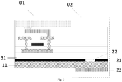
- the array substrate provided by the embodiment of the present disclosure includes: a base substrate 11, and a plurality of pixel elements 01 and a plurality of fingerprint recognition elements 02 which are located within a display region of the base substrate 11.
- the fingerprint recognition elements 02 includes: light-shielding layers 21 and photosensitive image sensors 23 that are located on the base substrate 11.
- the light-shielding layers 21 are provided with through holes 22 used to achieve small-aperture imaging.
- the orthographic projections of the through holes 22 on the base substrate 11 do not overlap with the orthographic projections of the pixel elements 01 on the base substrate 11.
- the photosensitive image sensors 23 are used to receive images of a fingerprint formed by means of the through holes 22.
- the array substrate by arranging the fingerprint recognition elements in the display region of the array substrate, the area of a non-display region of the array substrate may be reduced, which is advantageous for implementing a narrow-bezel design of the array substrate. Furthermore, the orthographic projections of the through holes in the fingerprint recognition elements on the base substrate do not overlap with the orthographic projections of the pixel elements on the base substrate, so that the aperture ratio of the array substrate may not be affected, and various film layers in the pixel elements are prevented from shielding the fingerprint recognition elements. Therefore, the array substrate can achieve a fingerprint recognition function conveniently.
- the array substrate further includes: wires 12 connected with the pixel elements 01. Since the wires 12 are generally arranged in gaps between adjacent pixel elements 01, in order to prevent the wires 12 from shielding the fingerprint recognition elements, the orthographic projections of the through holes 22 on the base substrate 11 do not overlap with the orthographic projections of the wires 12 on the base substrate 11.
- OLED organic light emitting diode
- the pixel elements include OLEDs and pixel circuits used to drive the OLEDs to emit light.
- the above wires are signal lines used to input various signals to the pixel circuits, such as gate lines GT, data lines DT, high-voltage signal lines and reference voltage signal lines, etc.
- the pixel elements emit light to irradiate fingerprints, and the fingerprints reflect the irradiating light and form images on the photosensitive image sensors by means of the through holes arranged on the light-shielding layers, so that the images formed on the photosensitive image sensors may be acquired, and a fingerprint image with a complete fingerprint may be determined according to the acquired images formed on the photosensitive image sensors, so as to process fingerprint information, thereby achieving fingerprint recognition.
- the through holes are manufactured on the light-shielding layers located on the base substrate.
- the through holes on the light-shielding layers may be arranged at positions that are not shielded by the pixel elements and the wires connected with the pixel elements.
- the diameter of the through holes shall meet the requirements of a small-aperture imaging principle on a small-aperture diameter.
- the specific size of the diameter of the through holes may be designed and determined according to an actual application environment, and is not specifically limited here.
- the diameter of the through holes shall be as small as possible, but it may not be too small.
- An extremely small diameter of the through holes will easily cause extremely low illuminance on the surfaces of the photosensitive image sensors, and it is difficult to extract imaging data. Therefore, in specific implementation, in the above array substrate provided by the embodiment of the present disclosure, the value range of the diameter of each through hole is set to be from 5 microns to 20 microns in combination with the photosensitivity of the photosensitive image sensors according to an actual structure of the array substrate and a film layer stacking mode used.
- the fingerprint recognition elements may be uniformly located in the whole array substrate, or may be only located in a certain specific region in the array substrate, and this is not specifically limited thereto.
- the through holes may be uniformly arranged on the base substrate.
- images formed in the center of a small aperture are relatively clear, and are blurred when being close to the edge, so that the through holes in the fingerprint recognition elements may be arranged in an array manner.
- the fingerprint may be partitioned, so that during imaging of the fingerprint, a formed image of each fingerprint recognition element needs to include a formed image of the adjacent fingerprint recognition element.
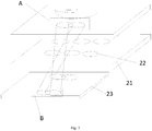
- a fingerprint overlapping region A exists, namely a common imaging portion exists. In this way, the fingerprint images formed by the fingerprint recognition elements are convenient to splice in the later image extraction and processing to be integrated into a complete and clear image.
- the array substrate provided by the embodiments of the present disclosure includes a plurality of fingerprint recognition elements.
- the various fingerprint recognition elements may be spaced by a certain distance, otherwise the images formed on the photosensitive image sensors by the through holes of the various fingerprint recognition elements may overlap. As shown in Fig. 3 , a formed image overlapping region B exists. In this way, the fingerprint images are difficult to separate when the imaging data on the photosensitive image sensors are processed.
- the center distance between any two adjacent through holes may be enabled to satisfy a formula: d ⁇ 3 h d D 2 h t + D ; where d represents the center distance between two adjacent through holes 22; D represents the diameter of the through holes 22; h d represents the distance from the lower surfaces of the light-shielding layers 21 to the upper surfaces of the photosensitive image sensors 23; and h t represents the thickness of the light-shielding layers 21.
- the fingerprint overlapping region A may exist, and then the complete and clear image may be obtained by processing the imaging data. Furthermore, there exist certain distance between every two adjacent through holes 22, so that the formed image overlapping region B does not exist in the images formed on the photosensitive image sensors 23, so that the fingerprint is recognized by extracting and processing the formed image data.
- region sizes of the images formed by fingerprint details (such as adjacent ridges and valleys) on the image sensors may correspond to the sizes of at least three pixel elements, so that the fingerprints may be accurately recognized.
- the light-shielding layers may be only located in a region where the fingerprint recognition elements are located, or may be deposited on the whole base substrate, so as to avoid the influence on the display characteristics of the array substrate. This is selected according to a specific use scene, and is not specifically limited here.
- the light-shielding layers 21 may be located on the side, provided with the pixel elements 01, of the base substrate 11. Further, in the above array substrate provided by the embodiment of the present disclosure, since the pixel elements include the pixel circuits, the pixel circuits may include thin film transistors, and the OLEDs are located on the sides, away from the base substrate, of the thin film transistors. The light-shielding layers 21 may be located on the side, provided with the thin film transistors, of the base substrate 11.
- the light-shielding layer 21 may be located between the base substrate 11 and the pixel element 01. Further, in specific implementation, as shown in Fig. 2A , the orthographic projection of the light-shielding layer 21 on the base substrate 11 may be enabled not to overlap with the orthographic projection of the pixel element 01 on the base substrate 11. Or, as shown in Fig. 5 , the orthographic projection of the light-shielding layer 21 on the base substrate 11 covers the orthographic projection of the pixel element 01 on the base substrate 11.
- a material of the light-shielding layers may include a metal material, or a non-metal material for light shielding.
- the through holes penetrating through the light-shielding layers are manufactured on the light-shielding layers by means of a mask.
- the array substrate further include: a low-temperature dielectric layer 31 located between the light-shielding layer 21 and the pixel element 01. Further, the low-temperature dielectric layers 31 are located between the thin film transistors and the light-shielding layers 21, so that the influence on a manufacturing process of the thin film transistors in the pixel elements may be avoided. Particularly, when the material of the light-shielding layers is the metal material, the low-temperature dielectric layers 31 may avoid the influence on the manufacturing process of the thin film transistors in the pixel elements.
- the array substrate may be a rigid array substrate.
- the base substrate may be a glass substrate, a sapphire substrate, a quartz substrate, a plastic substrate and the like.
- the array substrate may also be a flexible array substrate.
- the base substrate may be a flexible substrate, such as a PI substrate.
- it may also be other flexible material substrates, and is not limited here.
- the base substrate when the base substrate is the flexible substrate, it may include a flexible layer, or may include at least two flexible layers.
- the present disclosure is not limited thereto.
- the light-shielding layers may be arranged between the two flexible layers, so that the low-temperature dielectric layers may not be arranged additionally, which further reduces the thickness of the film layers in the array substrate.
- the photosensitive image sensor 23 may be located on the side, back onto the light-shielding layer 21, of the base substrate 11 and at a position corresponding to the through hole 22.
- the photosensitive image sensors and the light-shielding layers are respectively located on two sides of the base substrate, and the photosensitive image sensors are located at the positions corresponding to the through holes, so that images can be conveniently formed on the photosensitive image sensors.
- one photosensitive image sensor may be arranged in the array substrate. Images may be formed in all regions of the photosensitive image sensor by all the through holes, and then the images formed in all the regions of the photosensitive image sensor are processed, thereby achieving fingerprint recognition.
- a plurality of photosensitive image sensors may also be arranged in the array substrate. The photosensitive image sensors are in one-to-one correspondence to all the through holes, or one photosensitive image sensor corresponds to a plurality of through holes. This is set according to a specific application situation, and is not specifically limited.
- the photosensitive image sensors may include CCD photosensitive image sensors or CMOS photosensitive image sensors.
- the photosensitive image sensors may also be other photosensitive image sensors capable of recognizing the fingerprints, and are not specifically limited here.
- an embodiment of the present disclosure further provides a preparation method for an array substrate, including that: a plurality of pixel elements and a plurality of fingerprint recognition elements are formed in a display region of a base substrate.
- the fingerprint recognition elements include: light-shielding layers and photosensitive image sensors that are located on the base substrate.
- the light-shielding layers are provided with through holes used to achieve small-aperture imaging.
- the orthographic projections of the through holes on the base substrate do not overlap with the orthographic projections of the pixel elements on the base substrate.
- the photosensitive image sensors are used to receive images of a fingerprint formed by means of the through holes.
- the implementations of the preparation method for the array substrate may refer to the implementations of the above-mentioned array substrate, and repeated descriptions are omitted.
- the light-shielding layers may be arranged between the pixel elements and the base substrate.
- the preparation method provided by the embodiments of the present disclosure may specifically include the following steps.
- the light-shielding layers are formed on the base substrate.
- the light-shielding layers are patterned, and through holes are formed in a region where the fingerprint recognition elements are located.
- the orthographic projections of the through holes on the base substrate do not overlap with the orthographic projections of the pixel elements on the base substrate.
- Step S603 the pixel elements are formed on the light-shielding layers with the through holes.
- Step S603 may further include: wires connected with the pixel elements are formed.
- the orthographic projections of the through holes on the base substrate do not overlap with the orthographic projections of the wires on the base substrate.
- the photosensitive image sensors are arranged on the side, back onto the light-shielding layers, of the base substrate and at positions corresponding to the through holes.
- an embodiment of the present disclosure further provides a fingerprint recognition method using the above array substrate.
- the fingerprint recognition method may include the following steps.
- images formed on the photosensitive image sensors are acquired.
- the formed images are images formed on the photosensitive image sensors corresponding to the through holes by reflecting, by a fingerprint, light emitted by the pixel elements by means of the through holes.
- a fingerprint image with a complete fingerprint is determined according to the acquired images formed on the photosensitive image sensors. Specifically, the images formed on the photosensitive image sensors are spliced and integrated to obtain a complete fingerprint image.
- the implementations of the fingerprint recognition method may refer to the implementations of the above-mentioned array substrate, and repeated descriptions are omitted.
- an embodiment of the present disclosure further provides a display device, including any one of the above array substrates provided by the embodiments of the present disclosure.
- the problem solving principle of the display device is similar to that of the above-mentioned array substrate, so that the implementations of the display device may refer to the implementations of the array substrate, and repeated descriptions will be omitted.
- the display device may be: any product or component having a display function, such as a mobile phone, a tablet computer, a television, a display, a notebook computer, a digital photo frame and a navigator, etc.
- a display function such as a mobile phone, a tablet computer, a television, a display, a notebook computer, a digital photo frame and a navigator, etc.
- Other indispensable components of the display device are all understood by those skilled in the art, and are not described herein and should not be construed as limiting the present disclosure.
- the fingerprint recognition method, and the display device provided by the embodiments of the present disclosure, by arranging the fingerprint recognition elements in the display region of the array substrate, the area of a non-display region of the array substrate may be reduced, which is advantageous for implementing a narrow-bezel design of the array substrate. Furthermore, the orthographic projections of the through holes in the fingerprint recognition elements on the base substrate do not overlap with the orthographic projections of the pixel elements on the base substrate, so that the aperture ratio of the array substrate may not be affected, and various film layers in the pixel elements are also prevented from shielding the fingerprint recognition elements. Therefore, the array substrate can achieve a fingerprint recognition function conveniently.
Landscapes
- Engineering & Computer Science (AREA)
- Theoretical Computer Science (AREA)
- Inorganic Chemistry (AREA)
- Chemical & Material Sciences (AREA)
- General Engineering & Computer Science (AREA)
- Human Computer Interaction (AREA)
- Physics & Mathematics (AREA)
- General Physics & Mathematics (AREA)
- Life Sciences & Earth Sciences (AREA)
- Sustainable Development (AREA)
- Multimedia (AREA)
- Manufacturing & Machinery (AREA)
- Image Input (AREA)
- Electroluminescent Light Sources (AREA)
- Devices For Indicating Variable Information By Combining Individual Elements (AREA)
- Solid State Image Pick-Up Elements (AREA)
Applications Claiming Priority (2)
| Application Number | Priority Date | Filing Date | Title |
|---|---|---|---|
| CN201711338861.0A CN107832749B (zh) | 2017-12-14 | 2017-12-14 | 一种阵列基板、其制备方法、指纹识别方法及显示装置 |
| PCT/CN2018/118681 WO2019114572A1 (fr) | 2017-12-14 | 2018-11-30 | Substrat de réseau et son procédé de préparation, procédé de reconnaissance d'empreintes digitales et dispositif d'affichage |
Publications (3)
| Publication Number | Publication Date |
|---|---|
| EP3726418A1 true EP3726418A1 (fr) | 2020-10-21 |
| EP3726418A4 EP3726418A4 (fr) | 2021-08-25 |
| EP3726418B1 EP3726418B1 (fr) | 2025-10-29 |
Family
ID=61644416
Family Applications (1)
| Application Number | Title | Priority Date | Filing Date |
|---|---|---|---|
| EP18889260.8A Active EP3726418B1 (fr) | 2017-12-14 | 2018-11-30 | Substrat de réseau et son procédé de préparation, procédé de reconnaissance d'empreintes digitales et dispositif d'affichage |
Country Status (5)
| Country | Link |
|---|---|
| US (1) | US11100308B2 (fr) |
| EP (1) | EP3726418B1 (fr) |
| JP (2) | JP2021507324A (fr) |
| CN (1) | CN107832749B (fr) |
| WO (1) | WO2019114572A1 (fr) |
Families Citing this family (32)
| Publication number | Priority date | Publication date | Assignee | Title |
|---|---|---|---|---|
| CN107832749B (zh) | 2017-12-14 | 2021-01-22 | 京东方科技集团股份有限公司 | 一种阵列基板、其制备方法、指纹识别方法及显示装置 |
| US20190245011A1 (en) * | 2018-02-06 | 2019-08-08 | Innolux Corporation | Display device |
| CN108598111B (zh) * | 2018-04-24 | 2021-01-29 | 京东方科技集团股份有限公司 | 具有指纹识别功能的显示基板、方法及显示装置 |
| CN108733260B (zh) * | 2018-04-27 | 2021-11-19 | 武汉天马微电子有限公司 | 显示面板及显示装置 |
| WO2019214083A1 (fr) * | 2018-05-08 | 2019-11-14 | 华为技术有限公司 | Panneau d'affichage souple et terminal mobile |
| CN110536049A (zh) * | 2018-05-25 | 2019-12-03 | 印象认知(北京)科技有限公司 | 图像采集设备、图像采集方法、电子设备及成像装置 |
| CN109144311B (zh) | 2018-07-26 | 2022-06-07 | 京东方科技集团股份有限公司 | 显示基板、指纹识别方法、触控显示装置 |
| CN110162203B (zh) * | 2018-08-17 | 2022-11-18 | 京东方科技集团股份有限公司 | 阵列基板、显示面板、显示装置、指纹识别方法和触控方法 |
| CN108960215B (zh) * | 2018-08-30 | 2023-08-04 | 武汉华星光电技术有限公司 | 内嵌式面部识别显示面板、方法及液晶显示装置 |
| CN109032420B (zh) * | 2018-08-31 | 2021-04-16 | 京东方科技集团股份有限公司 | 显示装置及显示装置的操作方法 |
| CN109359638B (zh) * | 2018-12-18 | 2021-05-07 | 厦门天马微电子有限公司 | 滑动指纹识别方法、阵列基板、显示面板及显示装置 |
| CN109616015B (zh) * | 2019-01-29 | 2021-07-09 | 上海天马微电子有限公司 | 显示面板和显示装置 |
| CN111666781B (zh) * | 2019-03-05 | 2024-05-10 | 京东方科技集团股份有限公司 | 显示面板及其制作方法、显示装置 |
| CN109830495B (zh) | 2019-03-21 | 2021-10-08 | 京东方科技集团股份有限公司 | 阵列基板及其制备方法、显示装置及其成像方法 |
| CN109993141B (zh) * | 2019-04-10 | 2021-09-03 | 京东方科技集团股份有限公司 | 一种oled显示面板、指纹识别方法和显示装置 |
| CN109977932B (zh) * | 2019-05-14 | 2021-04-20 | 合肥京东方光电科技有限公司 | 一种指纹识别显示基板、显示面板、显示装置 |
| CN110190069B (zh) * | 2019-05-22 | 2021-08-03 | 武汉华星光电技术有限公司 | 阵列基板及其制备方法 |
| CN110164937A (zh) * | 2019-05-30 | 2019-08-23 | 武汉华星光电半导体显示技术有限公司 | Oled显示面板 |
| CN110277430A (zh) * | 2019-06-26 | 2019-09-24 | 上海天马有机发光显示技术有限公司 | 一种显示面板、其制备方法及显示装置 |
| CN110491910B (zh) * | 2019-07-30 | 2022-04-26 | 武汉华星光电半导体显示技术有限公司 | 一种显示面板及其制备方法、显示装置 |
| CN110415612B (zh) * | 2019-08-05 | 2022-07-08 | 京东方科技集团股份有限公司 | 显示面板、电子设备和显示面板的成像方法 |
| CN110596979B (zh) * | 2019-09-27 | 2022-07-08 | 厦门天马微电子有限公司 | 一种阵列基板及显示装置 |
| CN110866456B (zh) * | 2019-10-28 | 2023-12-12 | 武汉华星光电技术有限公司 | 屏下指纹识别装置、显示面板及显示装置 |
| CN110866506B (zh) * | 2019-11-20 | 2022-03-15 | 厦门天马微电子有限公司 | 一种显示面板和显示装置 |
| CN110970480A (zh) * | 2019-12-17 | 2020-04-07 | 京东方科技集团股份有限公司 | 一种显示面板及显示装置 |
| CN113490942B (zh) * | 2019-12-20 | 2025-03-14 | 京东方科技集团股份有限公司 | 显示基板及其制作方法、显示面板和显示装置 |
| KR20210112767A (ko) * | 2020-03-06 | 2021-09-15 | 삼성전자주식회사 | 전자 장치 및 전자 장치의 지문 인식 방법 |
| KR102893632B1 (ko) * | 2020-03-18 | 2025-12-01 | 삼성디스플레이 주식회사 | 표시 장치 |
| WO2022155871A1 (fr) * | 2021-01-22 | 2022-07-28 | 京东方科技集团股份有限公司 | Écran d'affichage et dispositif d'affichage |
| CN115933898A (zh) * | 2021-08-17 | 2023-04-07 | 京东方科技集团股份有限公司 | 一种触控显示面板和显示装置 |
| CN114242753B (zh) * | 2021-09-30 | 2025-08-19 | 湖北长江新型显示产业创新中心有限公司 | 显示面板和显示装置 |
| WO2023230805A1 (fr) * | 2022-05-31 | 2023-12-07 | 京东方科技集团股份有限公司 | Substrat d'affichage et dispositif d'affichage |
Family Cites Families (17)
| Publication number | Priority date | Publication date | Assignee | Title |
|---|---|---|---|---|
| USH665H (en) * | 1987-10-19 | 1989-08-01 | Bell Telephone Laboratories, Incorporated | Resistive field shields for high voltage devices |
| JP4087125B2 (ja) * | 2001-03-07 | 2008-05-21 | シャープ株式会社 | 凹凸パターン検出素子 |
| JP2010072722A (ja) * | 2008-09-16 | 2010-04-02 | Hitachi Maxell Ltd | 光学部品、撮像装置、生体情報取得装置、及び光学部品の製造方法 |
| TWI464491B (zh) * | 2011-11-08 | 2014-12-11 | Au Optronics Corp | 顯示裝置 |
| KR102007831B1 (ko) * | 2012-12-14 | 2019-08-06 | 엘지디스플레이 주식회사 | 네로우 베젤 타입 액정표시장치용 어레이 기판 |
| CN105989325A (zh) * | 2015-01-29 | 2016-10-05 | 深圳印象认知技术有限公司 | 蜂窝结构的指纹掌纹图像采集器及终端设备 |
| US10410033B2 (en) * | 2015-06-18 | 2019-09-10 | Shenzhen GOODIX Technology Co., Ltd. | Under-LCD screen optical sensor module for on-screen fingerprint sensing |
| US10176355B2 (en) * | 2015-12-03 | 2019-01-08 | Synaptics Incorporated | Optical sensor for integration in a display |
| CN105678255B (zh) | 2016-01-04 | 2019-01-08 | 京东方科技集团股份有限公司 | 一种光学式指纹识别显示屏及显示装置 |
| CN106096595B (zh) | 2016-08-08 | 2022-08-09 | 京东方科技集团股份有限公司 | 一种指纹识别模组、其制作方法及指纹识别显示装置 |
| KR102693504B1 (ko) * | 2016-09-26 | 2024-08-12 | 삼성디스플레이 주식회사 | 표시장치 및 그의 구동방법 |
| CN206193837U (zh) * | 2016-09-26 | 2017-05-24 | 惠州Tcl移动通信有限公司 | 移动终端及其指纹识别模组 |
| CN106773219B (zh) * | 2017-02-07 | 2019-11-05 | 京东方科技集团股份有限公司 | 一种显示装置 |
| CN107103307B (zh) * | 2017-05-23 | 2020-05-22 | 京东方科技集团股份有限公司 | 触控面板和显示装置 |
| CN107358216B (zh) * | 2017-07-20 | 2020-12-01 | 京东方科技集团股份有限公司 | 一种指纹采集模组、显示装置及指纹识别方法 |
| CN107832749B (zh) | 2017-12-14 | 2021-01-22 | 京东方科技集团股份有限公司 | 一种阵列基板、其制备方法、指纹识别方法及显示装置 |
| CN108073900B (zh) * | 2017-12-14 | 2021-01-08 | 京东方科技集团股份有限公司 | 用于指纹识别的柔性显示面板、显示装置及指纹识别方法 |
-
2017
- 2017-12-14 CN CN201711338861.0A patent/CN107832749B/zh active Active
-
2018
- 2018-11-30 JP JP2019561147A patent/JP2021507324A/ja active Pending
- 2018-11-30 US US16/620,983 patent/US11100308B2/en active Active
- 2018-11-30 EP EP18889260.8A patent/EP3726418B1/fr active Active
- 2018-11-30 WO PCT/CN2018/118681 patent/WO2019114572A1/fr not_active Ceased
-
2024
- 2024-04-26 JP JP2024072616A patent/JP7699265B2/ja active Active
Also Published As
| Publication number | Publication date |
|---|---|
| EP3726418A4 (fr) | 2021-08-25 |
| JP2021507324A (ja) | 2021-02-22 |
| US11100308B2 (en) | 2021-08-24 |
| EP3726418B1 (fr) | 2025-10-29 |
| CN107832749B (zh) | 2021-01-22 |
| JP2024100781A (ja) | 2024-07-26 |
| US20200202099A1 (en) | 2020-06-25 |
| CN107832749A (zh) | 2018-03-23 |
| JP7699265B2 (ja) | 2025-06-26 |
| WO2019114572A1 (fr) | 2019-06-20 |
Similar Documents
| Publication | Publication Date | Title |
|---|---|---|
| US11100308B2 (en) | Array substrate and preparation method therefor, fingerprint recognition method, and display device | |
| US10545616B2 (en) | Touch display panel, flexible display panel and display apparatus | |
| CN106773219B (zh) | 一种显示装置 | |
| CN106775109B (zh) | 触控基板及其驱动方法、显示装置 | |
| US20200134281A1 (en) | Display panel, display device, and method for driving the same | |
| US20190187756A1 (en) | Flexible display panel for fingerprint recognition, display device and fingerprint recognition method | |
| CN106886341B (zh) | 显示基板及显示装置 | |
| CN107122750B (zh) | 一种光学指纹识别装置及显示面板 | |
| US10489628B2 (en) | Fingerprint recognition device, method for fabricating the same and display device | |
| WO2019085968A1 (fr) | Module d'identification d'empreinte digitale, procédé d'identification d'empreinte digitale et appareil d'affichage | |
| US10714560B2 (en) | Flexible display panel including fingerprint recognition area and manufacturing method thereof | |
| US11367858B2 (en) | Display module and display device with through hole and two phase retarders | |
| US20180239455A1 (en) | Touch device and display device | |
| WO2017036079A1 (fr) | Élément de reconnaissance d'empreintes digitales, procédé de reconnaissance d'empreintes digitales, organe d'affichage et dispositif d'affichage | |
| US20190079628A1 (en) | Sensing panel, and display device and driving method thereof | |
| US20160216817A1 (en) | Array substrate, method for producing the same and display apparatus | |
| CN110162203B (zh) | 阵列基板、显示面板、显示装置、指纹识别方法和触控方法 | |
| WO2016115780A1 (fr) | Dispositif de reconnaissance d'empreinte digitale et appareil tactile | |
| KR20190094287A (ko) | 표시 컴포넌트, 그 제조 방법 및 표시 장치 | |
| CN205788140U (zh) | 一种触控显示面板、柔性显示面板以及显示装置 | |
| CN105447484A (zh) | 一种阵列基板以及显示装置 | |
| CN116704563A (zh) | 指纹识别装置及其制作方法、电子设备 |
Legal Events
| Date | Code | Title | Description |
|---|---|---|---|
| STAA | Information on the status of an ep patent application or granted ep patent |
Free format text: STATUS: THE INTERNATIONAL PUBLICATION HAS BEEN MADE |
|
| PUAI | Public reference made under article 153(3) epc to a published international application that has entered the european phase |
Free format text: ORIGINAL CODE: 0009012 |
|
| STAA | Information on the status of an ep patent application or granted ep patent |
Free format text: STATUS: REQUEST FOR EXAMINATION WAS MADE |
|
| 17P | Request for examination filed |
Effective date: 20200331 |
|
| AK | Designated contracting states |
Kind code of ref document: A1 Designated state(s): AL AT BE BG CH CY CZ DE DK EE ES FI FR GB GR HR HU IE IS IT LI LT LU LV MC MK MT NL NO PL PT RO RS SE SI SK SM TR |
|
| AX | Request for extension of the european patent |
Extension state: BA ME |
|
| DAV | Request for validation of the european patent (deleted) | ||
| DAX | Request for extension of the european patent (deleted) | ||
| A4 | Supplementary search report drawn up and despatched |
Effective date: 20210728 |
|
| RIC1 | Information provided on ipc code assigned before grant |
Ipc: G06K 9/00 20060101AFI20210722BHEP Ipc: G06F 3/041 20060101ALI20210722BHEP Ipc: H01L 27/146 20060101ALI20210722BHEP Ipc: H01L 27/32 20060101ALN20210722BHEP |
|
| STAA | Information on the status of an ep patent application or granted ep patent |
Free format text: STATUS: EXAMINATION IS IN PROGRESS |
|
| 17Q | First examination report despatched |
Effective date: 20230707 |
|
| REG | Reference to a national code |
Ref country code: DE Ref legal event code: R079 Free format text: PREVIOUS MAIN CLASS: G06K0009000000 Ipc: G06V0040130000 Ref country code: DE Ref legal event code: R079 Ref document number: 602018086803 Country of ref document: DE Free format text: PREVIOUS MAIN CLASS: G06K0009000000 Ipc: G06V0040130000 |
|
| GRAP | Despatch of communication of intention to grant a patent |
Free format text: ORIGINAL CODE: EPIDOSNIGR1 |
|
| STAA | Information on the status of an ep patent application or granted ep patent |
Free format text: STATUS: GRANT OF PATENT IS INTENDED |
|
| RIC1 | Information provided on ipc code assigned before grant |
Ipc: H10K 59/65 20230101ALI20250512BHEP Ipc: H10F 39/00 20250101ALI20250512BHEP Ipc: G06V 40/13 20220101AFI20250512BHEP |
|
| INTG | Intention to grant announced |
Effective date: 20250526 |
|
| RAP3 | Party data changed (applicant data changed or rights of an application transferred) |
Owner name: BOE TECHNOLOGY GROUP CO., LTD. |
|
| GRAS | Grant fee paid |
Free format text: ORIGINAL CODE: EPIDOSNIGR3 |
|
| GRAA | (expected) grant |
Free format text: ORIGINAL CODE: 0009210 |
|
| STAA | Information on the status of an ep patent application or granted ep patent |
Free format text: STATUS: THE PATENT HAS BEEN GRANTED |
|
| AK | Designated contracting states |
Kind code of ref document: B1 Designated state(s): AL AT BE BG CH CY CZ DE DK EE ES FI FR GB GR HR HU IE IS IT LI LT LU LV MC MK MT NL NO PL PT RO RS SE SI SK SM TR |
|
| REG | Reference to a national code |
Ref country code: CH Ref legal event code: F10 Free format text: ST27 STATUS EVENT CODE: U-0-0-F10-F00 (AS PROVIDED BY THE NATIONAL OFFICE) Effective date: 20251029 Ref country code: GB Ref legal event code: FG4D |
|
| REG | Reference to a national code |
Ref country code: IE Ref legal event code: FG4D |
|
| REG | Reference to a national code |
Ref country code: DE Ref legal event code: R096 Ref document number: 602018086803 Country of ref document: DE |
|
| PGFP | Annual fee paid to national office [announced via postgrant information from national office to epo] |
Ref country code: DE Payment date: 20251119 Year of fee payment: 8 |
|
| PGFP | Annual fee paid to national office [announced via postgrant information from national office to epo] |
Ref country code: GB Payment date: 20251121 Year of fee payment: 8 |
|
| REG | Reference to a national code |
Ref country code: NL Ref legal event code: MP Effective date: 20251029 |
|
| PG25 | Lapsed in a contracting state [announced via postgrant information from national office to epo] |
Ref country code: ES Free format text: LAPSE BECAUSE OF FAILURE TO SUBMIT A TRANSLATION OF THE DESCRIPTION OR TO PAY THE FEE WITHIN THE PRESCRIBED TIME-LIMIT Effective date: 20251029 |
|
| REG | Reference to a national code |
Ref country code: LT Ref legal event code: MG9D |
|
| PG25 | Lapsed in a contracting state [announced via postgrant information from national office to epo] |
Ref country code: NO Free format text: LAPSE BECAUSE OF FAILURE TO SUBMIT A TRANSLATION OF THE DESCRIPTION OR TO PAY THE FEE WITHIN THE PRESCRIBED TIME-LIMIT Effective date: 20260129 |
|
| PG25 | Lapsed in a contracting state [announced via postgrant information from national office to epo] |
Ref country code: FI Free format text: LAPSE BECAUSE OF FAILURE TO SUBMIT A TRANSLATION OF THE DESCRIPTION OR TO PAY THE FEE WITHIN THE PRESCRIBED TIME-LIMIT Effective date: 20251029 Ref country code: AT Free format text: LAPSE BECAUSE OF FAILURE TO SUBMIT A TRANSLATION OF THE DESCRIPTION OR TO PAY THE FEE WITHIN THE PRESCRIBED TIME-LIMIT Effective date: 20251029 Ref country code: HR Free format text: LAPSE BECAUSE OF FAILURE TO SUBMIT A TRANSLATION OF THE DESCRIPTION OR TO PAY THE FEE WITHIN THE PRESCRIBED TIME-LIMIT Effective date: 20251029 |
|
| REG | Reference to a national code |
Ref country code: AT Ref legal event code: MK05 Ref document number: 1852546 Country of ref document: AT Kind code of ref document: T Effective date: 20251029 |
|
| PG25 | Lapsed in a contracting state [announced via postgrant information from national office to epo] |
Ref country code: NL Free format text: LAPSE BECAUSE OF FAILURE TO SUBMIT A TRANSLATION OF THE DESCRIPTION OR TO PAY THE FEE WITHIN THE PRESCRIBED TIME-LIMIT Effective date: 20251029 |
|
| PG25 | Lapsed in a contracting state [announced via postgrant information from national office to epo] |
Ref country code: RS Free format text: LAPSE BECAUSE OF FAILURE TO SUBMIT A TRANSLATION OF THE DESCRIPTION OR TO PAY THE FEE WITHIN THE PRESCRIBED TIME-LIMIT Effective date: 20260129 |
|
| PG25 | Lapsed in a contracting state [announced via postgrant information from national office to epo] |
Ref country code: IS Free format text: LAPSE BECAUSE OF FAILURE TO SUBMIT A TRANSLATION OF THE DESCRIPTION OR TO PAY THE FEE WITHIN THE PRESCRIBED TIME-LIMIT Effective date: 20260228 |
|
| PG25 | Lapsed in a contracting state [announced via postgrant information from national office to epo] |
Ref country code: PT Free format text: LAPSE BECAUSE OF FAILURE TO SUBMIT A TRANSLATION OF THE DESCRIPTION OR TO PAY THE FEE WITHIN THE PRESCRIBED TIME-LIMIT Effective date: 20260302 |
|
| PG25 | Lapsed in a contracting state [announced via postgrant information from national office to epo] |
Ref country code: PL Free format text: LAPSE BECAUSE OF FAILURE TO SUBMIT A TRANSLATION OF THE DESCRIPTION OR TO PAY THE FEE WITHIN THE PRESCRIBED TIME-LIMIT Effective date: 20251029 |
|
| PG25 | Lapsed in a contracting state [announced via postgrant information from national office to epo] |
Ref country code: LV Free format text: LAPSE BECAUSE OF FAILURE TO SUBMIT A TRANSLATION OF THE DESCRIPTION OR TO PAY THE FEE WITHIN THE PRESCRIBED TIME-LIMIT Effective date: 20251029 |