EP3729038B1 - Wellenfrontrekonstruktion für dielektrische beschichtungen mit beliebiger wellenlänge - Google Patents
Wellenfrontrekonstruktion für dielektrische beschichtungen mit beliebiger wellenlänge Download PDFInfo
- Publication number
- EP3729038B1 EP3729038B1 EP17825537.8A EP17825537A EP3729038B1 EP 3729038 B1 EP3729038 B1 EP 3729038B1 EP 17825537 A EP17825537 A EP 17825537A EP 3729038 B1 EP3729038 B1 EP 3729038B1
- Authority
- EP
- European Patent Office
- Prior art keywords
- wavenumber
- phase shift
- shift
- dielectric coating
- determining
- Prior art date
- Legal status (The legal status is an assumption and is not a legal conclusion. Google has not performed a legal analysis and makes no representation as to the accuracy of the status listed.)
- Active
Links
Images






Classifications
-
- G—PHYSICS
- G01—MEASURING; TESTING
- G01N—INVESTIGATING OR ANALYSING MATERIALS BY DETERMINING THEIR CHEMICAL OR PHYSICAL PROPERTIES
- G01N21/00—Investigating or analysing materials by the use of optical means, i.e. using sub-millimetre waves, infrared, visible or ultraviolet light
- G01N21/17—Systems in which incident light is modified in accordance with the properties of the material investigated
- G01N21/41—Refractivity; Phase-affecting properties, e.g. optical path length
-
- G—PHYSICS
- G01—MEASURING; TESTING
- G01M—TESTING STATIC OR DYNAMIC BALANCE OF MACHINES OR STRUCTURES; TESTING OF STRUCTURES OR APPARATUS, NOT OTHERWISE PROVIDED FOR
- G01M11/00—Testing of optical apparatus; Testing structures by optical methods not otherwise provided for
- G01M11/02—Testing optical properties
-
- G—PHYSICS
- G01—MEASURING; TESTING
- G01N—INVESTIGATING OR ANALYSING MATERIALS BY DETERMINING THEIR CHEMICAL OR PHYSICAL PROPERTIES
- G01N21/00—Investigating or analysing materials by the use of optical means, i.e. using sub-millimetre waves, infrared, visible or ultraviolet light
- G01N21/84—Systems specially adapted for particular applications
- G01N21/8422—Investigating thin films, e.g. matrix isolation method
-
- G—PHYSICS
- G02—OPTICS
- G02B—OPTICAL ELEMENTS, SYSTEMS OR APPARATUS
- G02B1/00—Optical elements characterised by the material of which they are made; Optical coatings for optical elements
- G02B1/10—Optical coatings produced by application to, or surface treatment of, optical elements
-
- G—PHYSICS
- G01—MEASURING; TESTING
- G01N—INVESTIGATING OR ANALYSING MATERIALS BY DETERMINING THEIR CHEMICAL OR PHYSICAL PROPERTIES
- G01N21/00—Investigating or analysing materials by the use of optical means, i.e. using sub-millimetre waves, infrared, visible or ultraviolet light
- G01N21/17—Systems in which incident light is modified in accordance with the properties of the material investigated
- G01N21/41—Refractivity; Phase-affecting properties, e.g. optical path length
- G01N2021/4173—Phase distribution
Definitions
- This application relates to methods, processes, and apparatus for reconstruction of the wave front reflected/transmitted by dielectric coatings at arbitrary wavelength and for designing dielectric coatings robust to thickness errors.
- the application relates to a method of determining a phase shift caused by reflection at, or transmission through, a dielectric coating as function of wavenumber and to a method of determining a layer design for a dielectric coating, and to corresponding apparatus.
- Dielectric coatings are commonly used in many optical systems and optical instruments. These dielectric coatings have a significant wavelength dependent contribution to the overall image quality budget. Although it has been known since the 1950's that dielectric coatings, by design, will introduce wavelength dependent phase shifts to incoming wave fronts, this issue has to the inventor's knowledge not been addressed in the scientific literature.
- phase shift in reflection and transmission may depart from the as-designed phase shift due to manufacturing errors, and it may even be the case that structures are imprinted on the dielectric coating's reflected/transmitted wave front during the coating manufacturing process.
- the impact on the performance of the optical system including dielectric coatings may or may not be catastrophic depending on the robustness of the coatings design against manufacturing errors and on the design itself.
- Known techniques for determining the phase of light after reflection/transmission by a dielectric coating include ellipsometry and spectral reflectance/transmittance.
- the former technique necessitates a priori knowledge of the exact design of the dielectric coating and access to a wavelength scanning ellipsometer.
- the latter technique is based on Kramers-Kronig relations. It again requires a priori knowledge of the exact design of the dielectric coating and moreover provides non-unique solutions leading to ambiguities on the actual phase shift of the dielectric coating.
- the present document proposes a method of determining a phase shift caused by reflection at, or transmission through, a dielectric coating as function of wavenumber, corresponding apparatus, corresponding computer-executable program, and corresponding computer-readable storage media, having the features of the respective independent claims.
- the dependent claims relate to preferred embodiments.
- An aspect of the disclosure relates to a method of determining a phase shift caused by reflection at, or transmission through, a dielectric coating as function of wavenumber.
- the method includes obtaining a nominal phase shift ( ⁇ c ( k )) for the dielectric coating as function of wavenumber.
- the nominal phase shift is a known phase shift that is applied to a wave front in reflection or transmission by the dielectric coating as designed.
- the nominal phase shift may be provided by a manufacturer of the dielectric coating, for example.
- the nominal phase shift may be given for normal incidence or may be given for plurality of directions of incidence.
- the method further includes determining a first wavenumber and a second wavenumber for performing measurements of phase shift at these wavenumbers, based on the nominal phase shift.
- the method further includes determining a wavenumber shift based on a first measurement of phase shift at the first wavenumber, a second measurement of phase shift at the second wavenumber, and the nominal phase shift as function of wavenumber.
- the wavenumber shift may emulate a phase shift resulting from thickness variations in the dielectric coating.
- the method yet further includes determining the phase shift ( ⁇ r ( k ) or ⁇ t ( k )) as function of wavenumber based on the wavenumber shift and the nominal phase shift.
- the phase shift may relate to a wave front error (WFE).
- the determined phase shift may be an actual, or as-manufactured, phase shift of the dielectric coating.
- the phase shift as function of wavenumber may include a first portion ( ⁇ c ′ k ) resulting from thickness variations in the dielectric coating and a second portion ( ⁇ s ( k )) resulting from local deformation of the dielectric coating due to substrate deformation.
- the proposed method allows to infer the phase shift that is applied by an as-manufactured dielectric coating (e.g., coating stack) to a wave front in reflection or transmission.
- an as-manufactured dielectric coating e.g., coating stack
- Only minimal knowledge of the coating design and wave front measurements at two suitably chosen wavelengths are necessary for achieving this aim.
- the as-manufactured phase shift can be determined even if details of the coating stack are unknown (e.g., since they are retained by the manufacturer of the coating as part of his intellectual property).
- the accuracy of wave front measurements can be improved by taking into account the actual phase shift that is induced by the as-manufactured dielectric coating, instead of only considering the as-designed phase shift.
- the proposed method can be applied to any optical instrument or application that employs dielectric coatings.
- the method may further include determining an estimate of the wavenumber shift based on a simulation of a deviation of the dielectric coating from an as-designed configuration thereof.
- the simulation may involve perturbing the as-designed configuration of the dielectric coating.
- determining the first wavenumber and the second wavenumber may be further based on the estimate of the wavenumber shift.
- the wavenumber shift may be determined iteratively.
- the determining the phase shift as function of wavenumber based on the wavenumber shift and the nominal phase shift includes determining a first contribution to the phase shift as function of wavenumber, the first contribution depending on thickness variations of stacked layers of the dielectric coating from their respective nominal thickness.
- the determining the phase shift as function of wavenumber based on the wavenumber shift and the nominal phase shift yet further includes determining a second contribution to the phase shift as function of wavenumber, the second contribution depending on local deformation of the dielectric coating due to substrate deformation. Then, the phase shift as function of wavenumber may be determined based on the first contribution and the second contribution.
- the phase shift as function of wavenumber is based on a sum of the first contribution and the second contribution.
- the method may further include determining the first contribution by shifting the nominal phase shift as function of wavenumber by the wavenumber shift, such that the first contribution, at a given wavenumber, is given by the nominal phase shift at a shifted wavenumber that is obtained by shifting the given wavenumber by the wavenumber shift.
- the method may further include determining a total optical path difference that is caused by local deformation of the dielectric coating based on the first measurement of phase shift at the first wavenumber, the second measurement of phase shift at the second wavenumber, and the nominal phase shift. Then, the phase shift as function of wavenumber may be determined further based on the total optical path difference. Determining the second contribution may involve obtaining a product of the total optical path difference and the wavenumber. Thereby, the proposed method can also account for irregularities of the substrate on which the dielectric coating is provided.
- the steps of determining the wavenumber shift and determining the phase shift as function of wavenumber may be performed for each of a plurality of points on a surface of the dielectric coating. Thereby, a map of the phase shift across the surface or part of the surface of the dielectric coating may be obtained. Further, the steps of determining the wavenumber shift and determining the phase shift as function of wavenumber may be performed for each of a plurality of angles of incidence at the dielectric coating.
- the method may further include determining a phase shift at a third wavenumber that is different from both the first and second wavenumbers, based on the phase shift as function of wavenumber and the third wavenumber. Since the proposed method provides the phase shift as function of wavenumber, the phase shift (and thus the deformation of the wave front) can be calculated for any arbitrary wavenumber of interest.
- the method may further include obtaining a measured wave front after reflection by, or transmission through, the dielectric coating at the third wavenumber. Then, the method may yet further include determining a final output indicative of or depending on the measured wave front, based on the determined phase shift at the third wavenumber. This may involve calibrating the measurement based on the determined phase shift at the third wavenumber, correcting the measured wave front based on the determined phase shift at the third wavenumber, and/or modifying a quantity derived from the measured wave front based on the determined phase shift at the third wavenumber.
- the method may further include performing the first measurement of phase shift at the first wavenumber and the second measurement of phase shift at the second wavenumber. This may involve wave front measurements or wave front error measurements at the first and second wavenumbers.
- the method may further include obtaining design information relating to the dielectric coating. Then, the method may yet further include determining the nominal phase shift for the dielectric coating as function of wavenumber based on the design information.
- the dielectric coating may include a plurality of stacked layers.
- the plurality of stacked layers may be composed of different materials. Further, the plurality of layers may be supported by a substrate, e.g., may be stacked on the substrate.
- the design information may include a total optical thickness of the dielectric coating.
- the phase shift may further be a function of an angle of incidence at the dielectric coating.
- the method may further include correcting the phase shift as function of wavenumber based on a first spectral profile of a first light source that is used for the first measurement and/or a second spectral profile of a second light source that is used for the second measurement. Thereby, any deviation of the spectra of the first and second light sources from line spectra may be accounted for.
- the method may further include obtaining a result of a fourth measurement of a wave front after reflection by, or transmission through, the dielectric coating at a fourth wavenumber, the fourth wavenumber being different from the first and second wavenumbers. Then, the method may further include reconstructing the wave front after reflection by, or transmission through, the dielectric coating at the fourth wavenumber using the determined wavenumber shift and the nominal phase shift. The method may yet further include correcting the determined wavenumber shift based on a comparison of the measured and reconstructed wave fronts at the fourth wavenumber. Thereby, the determined wavenumber shift may be further refined and accuracy of the overall calculation of the phase shift may be increased.
- Another aspect of the disclosure relates to an apparatus for determining a phase shift caused by reflection at, or transmission through, a dielectric coating as a function of wavenumber, the apparatus comprising one or more processors adapted to perform the method of the above aspect and its embodiments.
- Another aspect of the disclosure relates to a computer-executable program that, when executed by a processor, causes the processor to perform the method of the above aspect and its embodiments.
- Another aspect of the disclosure relates to a computer-readable storage medium storing the computer-executable program according to the preceding aspect.
- An example suitable for understanding the invention of the disclosure relates to a method of determining a layer design for a dielectric coating.
- the dielectric coating may comprise a plurality of stacked layers.
- the method may include determining a plurality of layer designs that are in conformity with a desired optical property of the dielectric coating (e.g., a spectral reflectance R).
- the method may further include determining, for each of the layer designs, a metric Z that depends on the total optical thickness of the dielectric coating according to that layer design and a bandwidth of interest, in terms of wavenumbers, for which the dielectric coating is intended for use.
- the method may yet further include selecting, as a final layer design for the dielectric coating, that layer design among the plurality of layer designs that has the smallest value of the metric Z.
- the bandwidth of interest may be a pre-set parameter in accordance with a desired use of the dielectric coating.
- the proposed method aids the design of dielectric coatings with relaxed tolerance on thickness error.
- a function of wavenumber is implicitly also a function of wavelength, and vice versa.
- the present disclosure addresses the problem in dielectric coatings that the phase shift departure of the as-manufactured dielectric coating departs from the as-designed phase shift.
- the phase shift is defined as the phase in reflection or in transmission added by a dielectric coating to an incoming wave front.
- the present disclosure proposes a process enabling the design of dielectric coatings that are robust with respect to thickness errors from the phase shift point of view.
- the present disclosure further proposes a process for the reconstruction of the total phase of a wave front in reflection and transmission when reflected or transmitted by a dielectric coating for any arbitrary wavelength ⁇ , with minimum prior knowledge on the details (e.g., layers definition) of the design of the dielectric coating.
- the proposed process only requires minimal knowledge on the as-designed dielectric coating and access to a wave front sensor with at least two wavelengths. Higher accuracy of the phase reconstruction of the reflected/transmitted wave front can be achieved if the wavelengths of the wave front sensor can be tuned.
- the process for the reconstruction of the total phase of a wave front in reflection and transmission when reflected or transmitted by a dielectric coating for any arbitrary wavelength ⁇ is based on the following basic property of the phase shift of a dielectric coating when submitted to small changes in the thickness of its layers. Namely, as the inventor has demonstrated, the phase shift of the dielectric coating as-manufactured can be approximated by a constant wavenumber shift ⁇ k applied to the phase shift of the dielectric coating as-designed.
- the coating non-uniformities introduced during manufacturing will have an impact on ⁇ but a negligible one on the spectral reflectance [Strojnik, 1995].
- the actual value of ⁇ is dependent on ⁇ , on the spatial coordinates on the coated surface and on the angle of incidence ⁇ .
- the nature of the phase shift variation depends uniquely on the exact definition of the coating stack.
- the elements of the matrix M ( X ) are dependent on the actual refractive index n i and thickness t i of each layer of the coating stack.
- the pair ( n i , t i ) can be determined experimentally using ellipsometry [Oreb, et al., 1999].
- LIGO Laser Interferometer Gravitational-Wave Observatory
- the characterization of ⁇ is of primordial importance for the measurement of ⁇ in spectroscopy using Fabry-Perot interferometers.
- This approach has two major drawbacks as far as, e.g., ESA's Euclid project is concerned. Namely, the resulting ⁇ is not unique [Tikhonravov, et al., 1997], and the measured R ( ⁇ ) is averaged over an area larger than the sampling needed to retrieve the medium and high spatial frequencies.
- the available information includes: wave front error maps at two wavelengths in transmission and reflection of the dichroic assembly (with beam splitter coating and anti-reflection coating) at room temperature, at normal incidence with a 32 ⁇ 32 pixels resolution, the as-designed phase shift ⁇ c ( ⁇ ) at normal incidence, the as-designed spectral reflectance R ( ⁇ ) for different angles of incidence for the s and p polarizations, the as-designed total thickness of the coating stack, and the as-designed total thickness of each material in the coating stack.
- wave front error maps at two wavelengths in transmission and reflection of the dichroic assembly (with beam splitter coating and anti-reflection coating) at room temperature, at normal incidence with a 32 ⁇ 32 pixels resolution
- the as-designed phase shift ⁇ c ( ⁇ ) at normal incidence the as-designed spectral reflectance R ( ⁇ ) for different angles of incidence for the s and p polarizations
- the as-designed total thickness of the coating stack the as-designed total thickness of each material in the coating
- the total phase ⁇ r ( k, ⁇ ) in reflection/transmission is the combination of the phase shift ⁇ c ′ k ⁇ of the coating considered as a stack of perfectly parallel layers and the phase ⁇ s ( k, ⁇ ) induced by local deformation of the coating layers due to substrate deformation.
- ⁇ r k ⁇ ⁇ c ′ k ⁇ + ⁇ s k ⁇ with ⁇ the angle of incidence on the first (e.g., uppermost) layer of the stack. If a given angle of incidence is considered, such as normal incidence, the argument ⁇ may be omitted.
- Eq. (1) ignores the effect of the local slopes due to the coating substrate [Strojnik, 1995]. Typically, the impact is negligible.
- the total phase in reflection/transmission comprises (provided that the term ⁇ s ( k, ⁇ ) is not neglected), a first contribution ⁇ c ′ that depends on thickness variations of stacked layers of the dielectric coating from their respective nominal thickness and a second contribution ⁇ s that depends on local deformation of the dielectric coating due to substrate deformation.
- the geometrical meaning of Eq. (3) is explained in Fig. 7 .
- phase shift with wavenumber k is dependent on the position of the zeros v j with respect to the k-axis.
- the phase shift is an oscillating function of k that does not change significantly in any wavenumber area.
- Fig. 8 The situation of all zeros v j being located in the lower half-plane is illustrated in Fig. 8 .
- manufactured coatings have zeros located on either half-plane of the wavenumber complex plane.
- the zeros of the functions f 1 and f 2 have the following properties:
- the average spacing between zeros is ⁇ / x with x the total optical path of the coating stack at normal incidence. Further, the range of values for ⁇ is limited to a narrow band around the real wavenumber axis.
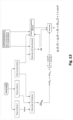
- Fig. 1 is a flowchart schematically illustrating an example of a method 100 of determining a phase shift caused by reflection at a dielectric coating ( ⁇ r ( k )) or transmission through the dielectric coating ( ⁇ t ( k )) as function of wavenumber according to embodiments of the disclosure. This method is at least partly based on the fact that Eq. (6) does hold.
- the dielectric coating comprises a plurality of stacked layers.
- each layer has constant thickness.
- the plurality of stacked layers may be composed of different materials. In general, the plurality of stacked layers may have different indexes of refraction.
- the plurality of stacked layers may be provided on a substrate.
- the dielectric coating may be used in reflection mode and in transmission mode. In either case, a wave front incident on the dielectric coating will undergo a phase shift. This phase shift may be known for the as-designed (i.e., nominal) dielectric coating. However, the as-manufactured dielectric coating may be different from the as-designed dielectric coating due to manufacturing errors.
- Method 100 seeks to determine the actual phase shift of the as-manufactured dielectric coating, as function of wavenumber. The actual phase shift may have a portion resulting from thickness variations of the layers of the dielectric coating (assuming layers of constant thickness) and a portion resulting from local deformations of the dielectric coating due to substrate deformation.
- the steps of method 100 may be performed for each of a plurality of points on the (surface of the) dielectric coating. Thereby, a map of the actual phase shift depending on position (x,y) on the dielectric coating can be obtained. Moreover, the steps of method 100 may be performed for each of a plurality of angles of incidence. Alternatively, the actual phase shift for a given angle of incidence may be analytically derived from the actual phase shift at another angle of incidence, e.g., normal incidence.
- a nominal phase shift ⁇ c ( k ) for the dielectric coating as function of wavenumber is obtained.
- the nominal phase shift is the (known) phase shift that would be applied to a wave front in reflection or transmission by the as-designed dielectric coating.
- the nominal phase shift may be given for normal incidence of light (e.g., of the wave front) on the dielectric coating.
- the nominal phase shift may be given for a plurality of distinct angles of incidence. In any case, either information is sufficient for determining the nominal phase shift at an arbitrary angle of incidence, e.g., via analytic relationships or interpolation.
- the nominal phase shift ⁇ c ( k ) may be provided by the manufacturer of the dielectric coating, for example.
- the nominal phase shift may be determined from design information relating to the dielectric coating.
- step S110 would include the sub-steps of obtaining the design information of the dielectric coating (e.g., a configuration of the as-designed dielectric coating), and determining the nominal phase shift (as function of wavenumber) based on the design information.
- the design information may include a total optical thickness of the dielectric coating (as designed), for example.
- a first wavenumber k 1 and a second wavenumber k 2 for performing measurements of phase shift are determined based on the nominal phase shift.
- N may be set to infinity
- N ⁇ .
- a finite number of higher orders of the Taylor expansion of ⁇ c ( k i + ⁇ k ) may be retained.
- R ( k ) includes higher order terms (second order or higher) of the Taylor expansion of the nominal phase shift at wavenumber k .
- step S120 may also involve selecting, from a plurality of wavenumbers at which wave front measurements can be performed, that pair of wavenumbers that minimizes ⁇ .
- a wavenumber shift ⁇ k is determined (e.g., calculated) based on a first measurement of phase shift at the first wavenumber (e.g., OPD 1 ), a second measurement of phase shift at the second wavenumber (e.g., OPD 2 ), and the nominal phase shift ⁇ c as function of wavenumber.
- This wavenumber shift ⁇ k emulates the phase shift resulting from thickness variations of the dielectric coating. That is, the as-manufactured phase shift at a given wavenumber k can be obtained by shifting the given wavenumber by the wavenumber shift ⁇ k and evaluating the nominal phase shift function ⁇ c at the shifted wavenumber k + ⁇ k.
- the wavenumber shift ⁇ k can be determined using Eq. (10), for example.
- step S130 may further involve determining (e.g., calculating) a total optical path difference l that is caused by local deformation of the dielectric coating (e.g., due to substrate irregularities) based on the first measurement of phase shift at the first wavenumber (e.g., OPD 1 ), the second measurement of phase shift at the second wavenumber (e.g., OPD 2 ), and the nominal phase shift ⁇ c .
- the total optical path difference l may be further determined based on the first wavenumber k 1 and the second wavenumber k 2 .
- the total optical path difference l can be derived from Eq. (10) and Eq. (7).
- step S130 may include performing the first measurement of phase shift at the first wave number k 1 and performing the second measurement of phase shift at the second wave number k 2 .
- the phase shift as function of wavenumber is determined based on the wavenumber shift ⁇ k and the nominal phase shift ⁇ c .
- This phase shift is the actual phase shift that is applied to a wave front by the as-manufactured dielectric coating.
- the phase shift may relate to a wave front error, i.e., to a deviation of the actual wave front (the wave front resulting from reflection at, or transmission through, the as-manufactured dielectric coating) from the wave front that would be obtained for the as-designed (nominal) dielectric coating.
- the phase shift as function of wavenumber is determined further based on the total optical path difference l .
- the second contribution of the phase shift may be determined based on the total optical path difference l .
- the phase shift is further a function of angle of incidence at the dielectric coating, i.e., depends on the angle of incidence.
- the functional dependence on the angle of incidence may be approximated by a cosine function.
- phase variation with the angle of incidence ⁇ will be provided below.
- phase shift as-designed, ⁇ c ( k, ⁇ ) requires to know the characteristic matrix of the coating accounting for the multi-reflections within each layer.
- the matrix in [Born, et al., 1999] cannot be used as it is valid only for a single reflection for each layer.
- this wavenumber shift ⁇ k ⁇ is independent of the wavenumber shift ⁇ k : While the former implements (takes into account, or emulates) a difference in angle of incidence from an angle of incidence ⁇ 0 , the latter implements (takes into account, or emulates) deviations of the as-manufactured coating from the as-designed coating.
- the wavenumber shift ⁇ k ⁇ may be referred to as angular wavenumber shift, or the like.
- ⁇ k ⁇ ⁇ k ⁇ 0 ⁇ 1 ⁇ cos ⁇ 1 ⁇ cos ⁇ 0 with ⁇ k ⁇ 0 the wavenumber shift calculated for the angle of incidence ⁇ 0 .
- Eq. (14) is justified by the fact that the zeros spacing ⁇ / x of the coating stack will vary as cos( ⁇ ) since the total optical path will vary approximately as 1/cos( ⁇ ).
- the wavenumber shift ⁇ k ⁇ increases as cos( ⁇ ) increases and the variation is approximately linear.
- OPE optical path error
- Fig. 2 is a flowchart schematically illustrating an example of method 200, which is an implementation of step S120 in method 100 of Fig. 1 .
- an estimate of the wavenumber shift is determined based on a simulation of a deviation of the dielectric coating from an as-designed configuration thereof.
- the simulation may involve (analytically) perturbing the as-designed configuration of the dielectric coating.
- the first wavenumber and the second wavenumber are determined based on the nominal phase shift and the estimate of the wavenumber shift. That is, the first and second wavenumbers are determined further based on the estimate of the wavenumber shift.
- step S220 may also involve selecting, from a plurality of wavenumbers at which wave front measurements can be performed, that pair of wavenumbers that minimizes ⁇ .
- Fig. 3 is a flowchart schematically illustrating a method 300, which is an implementation of step S140 in method 100 of Fig. 1 .
- a first contribution to the phase shift as function of wavenumber is determined.
- the first contribution depends on thickness variations of stacked layers of the dielectric coating from their respective nominal thickness. That is, the first contribution is that contribution to the total phase shift that depends on thickness variations (variations of constant-thickness layers from their nominal thickness) of the stacked layers of the dielectric coating.
- the first contribution can be determined by shifting the nominal phase shift as function of wavenumber by the wavenumber shift. Accordingly, the first contribution, at a given wavenumber, would be given by the nominal phase shift evaluated at a shifted wavenumber, wherein the shifted wavenumber is obtained by shifting the given wavenumber by the wavenumber shift.
- the wavenumber shift indicates by how much the actual wavenumber would have to be shifted so that evaluating the nominal phase shift function at the shifted wavenumber yields the actual phase shift for the as-manufactured dielectric coating.
- ⁇ c ( k ) indicates the nominal phase shift and ⁇ c ′ k indicates the first contribution
- a second contribution to the phase shift as function of wavenumber is determined.
- the second contribution depends on local deformation of the dielectric coating due to substrate deformation. That is, the second contribution is that contribution to the total phase shift that depends on local deformation of the dielectric coating due to substrate deformation.
- determining the second contribution ⁇ s ( k ) may involve obtaining a product of the total optical path difference l and the wavenumber k.
- the phase shift as function of wavenumber is determined based on the first contribution and the second contribution.
- the phase shift may depend on a sum of the first and second contributions.
- Fig. 4 is a flowchart schematically illustrating an example of method 400 implementing steps according to embodiments of the disclosure that may be performed in conjunction with (e.g., subsequent to) the steps in the flowchart of Fig. 1 .
- a result of a fourth measurement of a wave front after reflection by, or transmission through, the dielectric coating at a fourth wavenumber k 4 is obtained.
- the fourth wavenumber k 4 is different from the first and second wavenumbers k 1 , k 2 .
- a wave front after reflection by, or transmission through, the dielectric coating at the fourth wavenumber is reconstructed using the determined wavenumber shift ⁇ k and the nominal phase shift ⁇ c ( k ) .
- This may involve determining (e.g., calculating) the phase shift ⁇ r ( k 4 ) at the fourth wavenumber and determining an outgoing wave front using the (known) incoming wave front and the phase shift ⁇ r ( k 4 ) at the fourth wavenumber, e.g., by adding the phase shift to the incoming wave front for each location on the coating.
- the determined wavenumber shift ⁇ k is corrected based on a comparison of the measured and reconstructed wave fronts at the fourth wavenumber k 4 .
- the corrected wavenumber shift may then be used instead of the wavenumber shift determined at step S130 of method 100, e.g., in step S140 of method 100 and/or in the steps of method 500 described below.
- Fig. 5 is a flowchart schematically illustrating an example of method 500 implementing further steps according to embodiments of the disclosure that may be performed in conjunction with (e.g., subsequent to) the steps in the flowchart of Fig. 1 .
- a phase shift at a third wavenumber k 3 that is different from both the first and second wavenumbers k 1 , k 2 is determined, based on the phase shift ⁇ r ( k ) as function of wavenumber and the third wavenumber k 3 , e.g., by evaluating the phase shift ⁇ r ( k ) as function of wavenumber at the third wavenumber k 3 .
- step S520 a measured wave front after reflection by, or transmission through, the dielectric coating at the third wavenumber k 3 is obtained.
- a final output indicative of or depending on the measured wave front is determined, based on the determined phase shift ⁇ r ( k 3 ) at the third wavenumber k 3 .
- This may involve calibrating the measurement of the wave front at the third wavenumber k 3 based on the determined phase shift ⁇ r ( k 3 ) at the third wavenumber k 3 , correcting the measured wave front at the third wavenumber k 3 based on the determined phase shift ⁇ r ( k 3 ) at the third wavenumber k 3 , and/or modifying (e.g., correcting) a quantity derived from the measured wave front based on the determined phase shift ⁇ r ( k 3 ) at the third wavenumber k 3 .
- Fig. 6 is a flowchart schematically illustrating an example of a method 600 of determining a layer design for a dielectric coating according to embodiments of the disclosure.
- the dielectric coating comprises a plurality of stacked layers, e.g., stacked on a substrate.
- a plurality of layer designs are determined that are in conformity with a desired optical property of the dielectric coating.
- the desired optical property may be a certain spectral reflectance, for example.
- a metric Z is determined for each of the layer designs.
- the metric Z depends on the total optical thickness x of the dielectric coating according to the respective layer design and a bandwidth ⁇ k of interest, in terms of wavenumbers, for which the dielectric coating is intended for use.
- step S630 that layer design among the plurality of layer designs is selected as a final layer design for the dielectric coating, that has the smallest value of the metric Z.
- the reconstructed wave front maps can be used to retrieve the final performance of an optical system including a dielectric coating.
- the optical system can be an imaging system, a spectrometer, an interferometer etc.
- any optical application using dielectric coatings can profit from the methods and procedures of the present disclosure.
- the accuracy of the reconstruction depends on the accuracy of the WFE measurement, the value of ⁇ (the lower the better), and the intrinsic error of the approximation of the as-manufactured coating phase shift by a shift of the as-designed phase shift.
- ⁇ c phase shift for discrete values of the angle of incidence ⁇ (as many as necessary).
- the following information is needed: the total mechanical thickness of the coating, the materials used in the coating (i.e., their optical properties, e.g., indexes of refraction), and the total mechanical thickness of each material in the as-designed coating.
- a sensitivity analysis of the phase versus the layers' thickness error has been performed. The analysis is divided in two steps: First, a constant change of thickness is applied to each layer of the coating stack. The values selected for the change are, e.g., 0.2%,0.5%, 1% and 3%. Second, a Monte-Carlo analysis is performed in which the thickness of each individual layer departs randomly from its as-designed value with a standard deviation of ⁇ 0.3%. This procedure may be used for estimating the wavenumber shift in step S210 of method 200, for example.
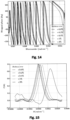
- Fig. 14 shows the wrapped phase for different thickness errors, for ⁇ ⁇ [550 nm, 900 nm]. From this figure, it can be concluded that a positive relative increase of the coating stack thickness induces a positive wavenumber shift ⁇ k max > 0. By symmetry it is assumed that for thinner coating stacks one would obtain ⁇ k max ⁇ 0.
- Fig. 15 shows the normalized cross-correlation factor C ( ⁇ k ) at different thickness errors, for ⁇ ⁇ [550 nm, 900 nm].
- OPE optical path error
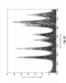
- the OPE for 200 runs of the Monte-Carlo analysis is shown in Fig. 18 , which shows the OPE as function of wavelength.
- the absolute OPE can reach very high values (e.g., > 60 nm) in some cases.
- the model accuracy is thus highly dependent on which layers are the most perturbed.
- the averaged (or mean) OPE over the band ⁇ ⁇ [550nm; 900nm] amounts to 5 nm ⁇ 2 nm and OPE ⁇ 12 nm.
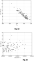
- OPE is correlated to C max .
- the correlation with ⁇ k max is less obvious.
- Fig. 20 shows the mean OPE, OPE for different values of ⁇ k max .
- ⁇ k max / k j « 1 is aimed to eliminate a source of bias in the phase calculation.
- the estimated value ⁇ k max 4.18 ⁇ 10 -5 rad. nm -1 is used to assess the ratio ⁇ k max / k j which is linear with ⁇ .
- This value of ⁇ k corresponds to C max for a thickness error of 0.5%.
- Eq. (14) can be applied to both polarizations.
- the wavenumber shift ⁇ k ⁇ to be applied to account for the angle of incidence ⁇ will be different depending on the polarization.
- the phase shift must be determined for the two polarizations independently for a given angle of incidence ⁇ 0 so that the terms ⁇ k TM ( ⁇ 0 ) and ⁇ k TE ( ⁇ 0 ) can be determined.
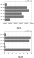
- the remnant defocus term added in the l map is about ⁇ 13.04 ⁇ 5.55 2 3 ⁇ 5.4 nm RMS.
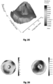
- Fig. 25 shows the WFE map at 595 nm without tilt. The scale is in waves.
- the actual wavelengths are derived from the spectral profile of the laser diodes.
- the actual wavelengths may be the centroid wavelengths for each source. In the remainder of the present disclosure, reference will be made to the theoretical wavelengths for simplicity. For the calculations the actual values will be used.
- the statistics of the surface defects map l are 23.7 nm RMS and 123 nm Peak-to-valley (PtV). It is worth noting that the WFE map l is comparable both in statistics and features to the Surface Figure Error (SFE) map of the bare surface (without coating) measured over a diameter of 113 mm while the l map covers an area of ⁇ 100 mm, giving confidence in the correctness of the calculations.
- SFE Surface Figure Error
- the SFE map of the bare surface is illustrated in Fig. 27 . Before polishing the equivalent WFE is 24.4 nm RMS and 131.6 nm PtV in line with the values for the l map.
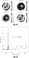
- Fig. 28 shows the RMS WFE as function of wavelength.
- Fig. 29 shows the residual maps obtained by subtracting the reconstructed WFE maps from the measured WFE maps. Residual statistics are also summarized in Table 4. These residuals are considered to assess the validity of the WFE map reconstruction according to the present disclosure. Further, Table 5 shows a comparison of RMS and PtV between the reconstructed and the measured WFE maps.
- the errors bars along the wavelength axis and RMS WFE axis are respectively given by the full width at half maximum of the diodes used in the measurement and the error budget on the WFE measurement (4 nm RMS).
- the determined wavenumber shift (e.g., determined at step S130 of method 100) may be corrected using a correction term that depends on a deviation of ⁇ from zero for the wavenumbers k 1 and k 2 actually used in the measurements.
- Fig. 31 shows the residual maps obtained by subtracting the reconstructed WFE maps (using the fine-tuned ⁇ k ) from the measured WFE maps.
- Fig. 32 shows the corrected maps for ⁇ k (left panel) and l (right panel) without piston.
- Fig. 33 shows the reconstructed WFE maps (using the fine-tuned ⁇ k ) .
- Fig. 34 shows the filtered residual maps with outlier points removed.
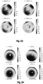
- the residual has a remnant focus (see Fig. 34 ) and a strong remnant tilt ( Fig. 24 ) in addition to the outliers points.
- the RMS of the residual drops to 11.6 nm RMS.
- the focus introduced in the map l is about 10 nm RMS. Removing this focus bias from the residual map and the focus from the measured map will lead to a residual of 3.5 nm RMS. Taking into account the 4 nm RMS measurement accuracy, the final residual amounts to 5.3 nm RMS.
- the present disclosure provides a method for reconstructing the phase of a wave front in reflection or transmission at a dielectric coating for arbitrary wavelength ⁇ .
- the proposed model is valid for any design of the dielectric coating (e.g., dichroic). Only the parameter values will change with the design.
- this simplified model is applied to the dichroic coating as-designed for Euclid's BDM.
- the phase in reflection in the visible channel is derived.
- Parameter values for the BDM dichroic are given in Table 8.
- Table 8 Parameter Unit TE TM ⁇ k c rad.nm -1 2.3 ⁇ 10 -5 ⁇ k ⁇ 0 rad.nm -1 -4.666 ⁇ 10 -5 not available ⁇ 0 degrees 12
- the term ⁇ k ⁇ ( P ) is calculated using Eq. (14).
- the as-designed phase shift at an angle ⁇ 0 > 0° should be used to derive ⁇ k ⁇ 0 so as to reduce the error on the calculated phase shift.
Landscapes
- Physics & Mathematics (AREA)
- General Physics & Mathematics (AREA)
- Chemical & Material Sciences (AREA)
- Analytical Chemistry (AREA)
- General Health & Medical Sciences (AREA)
- Life Sciences & Earth Sciences (AREA)
- Health & Medical Sciences (AREA)
- Biochemistry (AREA)
- Immunology (AREA)
- Pathology (AREA)
- Mathematical Physics (AREA)
- Optics & Photonics (AREA)
- Length Measuring Devices By Optical Means (AREA)
- Investigating Or Analysing Materials By Optical Means (AREA)
Claims (15)
- Verfahren (100) des Bestimmens einer Phasenverschiebung, die durch Reflexion an einer oder Transmission durch eine dielektrische(n) Beschichtung als Funktion der Wellenzahl verursacht ist, wobei das Verfahren (100) Folgendes umfasst:Erlangen (S110) einer Nenn-Phasenverschiebung für die dielektrische Beschichtung als Funktion der Wellenzahl, wobei die Nenn-Phasenverschiebung eine bekannte Phasenverschiebung ist, die auf eine Wellenfront bei Reflexion oder Transmission durch die dielektrische Beschichtung wie ausgelegt angewandt wird;Bestimmen (S120) einer ersten Wellenzahl und einer zweiten Wellenzahl zum Durchführen von Messungen der Phasenverschiebung bei diesen Wellenzahlen basierend auf der Nenn-Phasenverschiebung;Bestimmen (S130) einer Wellenzahlverschiebung basierend auf einer ersten Messung der Phasenverschiebung bei der ersten Wellenzahl, einer zweiten Messung der Phasenverschiebung bei der zweiten Wellenzahl und der Nenn-Phasenverschiebung als Funktion der Wellenzahl undBestimmen (S140) der Phasenverschiebung als Funktion der Wellenzahl basierend auf der Wellenzahlverschiebung und der Nenn-Phasenverschiebung,wobei das Bestimmen (S140) der Phasenverschiebung als Funktion der Wellenzahl basierend auf der Wellenzahlverschiebung und der Nenn-Phasenverschiebung Folgendes umfasst:Bestimmen (S310) eines ersten Beitrags zur Phasenverschiebung als Funktion der Wellenzahl, wobei der erste Beitrag von Dickenvariationen gestapelter Schichten der dielektrischen Beschichtung von ihrer jeweiligen Nenndicke abhängt; undBestimmen (S320) eines zweiten Beitrags zur Phasenverschiebung als Funktion der Wellenzahl, wobei der zweite Beitrag von lokaler Deformation der dielektrischen Beschichtung aufgrund von Substratdeformation abhängt, undwobei die Phasenverschiebung als Funktion der Wellenzahl auf einer Summe des ersten Beitrags und des zweiten Beitrags basiert.
- Verfahren (100) nach Anspruch 1, das ferner Folgendes umfasst:Bestimmen (S210) einer Abschätzung der Wellenzahlverschiebung basierend auf einer Simulation einer Abweichung der dielektrischen Beschichtung von einer Auslegungskonfiguration davon,wobei Bestimmen der ersten Wellenzahl und der zweiten Wellenzahl ferner auf der Abschätzung der Wellenzahlverschiebung basiert.
- Verfahren (100) nach Anspruch 1 oder 2, das ferner Folgendes umfasst:
Bestimmen des ersten Beitrags durch Verschieben der Nenn-Phasenverschiebung als Funktion der Wellenzahl um die Wellenzahlverschiebung derart, dass der erste Beitrag bei einer gegebenen Wellenzahl durch die Nenn-Phasenverschiebung bei einer verschobenen Wellenzahl gegeben ist, die durch Verschieben der gegebenen Wellenzahl um die Wellenzahlverschiebung erlangt wird. - Verfahren (100) nach irgendeinem der vorhergehenden Ansprüche, das ferner Folgendes umfasst:Bestimmen einer Gesamt-Strahlengangsdifferenz, die durch lokale Deformation der dielektrischen Beschichtung verursacht ist, basierend auf der ersten Messung der Phasenverschiebung bei der ersten Wellenzahl, der zweiten Messung der Phasenverschiebung bei der zweiten Wellenzahl und der Nenn-Phasenverschiebung,wobei optional die Phasenverschiebung als Funktion der Wellenzahl ferner basierend auf der Gesamt-Strahlengangsdifferenz bestimmt wird.
- Verfahren (100) nach Anspruch 4 wenn abhängig von Anspruch 3, wobei Bestimmen des zweiten Beitrags Erlangen eines Produkts der Gesamt-Strahlengangsdifferenz und der Wellenzahl einbezieht.
- Verfahren (100) nach irgendeinem der vorhergehenden Ansprüche, wobei die ersten und zweiten Wellenzahlen derart bestimmt werden, dass sie

- Verfahren (100) nach irgendeinem der vorhergehenden Ansprüche, wobei die Wellenzahlverschiebung bestimmt wird als

- Verfahren (100) nach irgendeinem der vorhergehenden Ansprüche, wobei die Schritte des Bestimmens der Wellenzahlverschiebung und Bestimmens der Phasenverschiebung als Funktion der Wellenzahl für jeden von mehreren Punkten auf einer Oberfläche der dielektrischen Beschichtung durchgeführt werden und/oder
wobei die Schritte des Bestimmens der Wellenzahlverschiebung und Bestimmens der Phasenverschiebung als Funktion der Wellenzahl für jeden von mehreren Einfallswinkel auf der dielektrischen Beschichtung durchgeführt werden. - Verfahren (100) nach irgendeinem der vorhergehenden Ansprüche, das ferner Bestimmen (S510) einer Phasenverschiebung bei einer dritten Wellenzahl, die sowohl von den ersten als auch zweiten Wellenzahlen verschieden ist, basierend auf der Phasenverschiebung als Funktion der Wellenzahl und der dritten Wellenzahl umfasst,
wobei optional das Verfahren (100) ferner Folgendes umfasst:Erlangen (S520) einer gemessenen Wellenfront nach Reflexion durch oder Transmission durch die dielektrische Beschichtung bei der dritten Wellenzahl;Bestimmen (S530) eines finalen Ausgangswertes kennzeichnend für die oder abhängig von der gemessene(n) Wellenfront basierend auf der bestimmten Phasenverschiebung bei der dritten Wellenzahl. - Verfahren (100) nach einem der vorhergehenden Ansprüche, das ferner Folgendes umfasst:Erlangen von Auslegungsinformationen bezüglich der dielektrischen Beschichtung undBestimmen der Nenn-Phasenverschiebung für die dielektrische Beschichtung als Funktion der Wellenzahl basierend auf den Auslegungsinformationen,wobei optional die dielektrische Beschichtung mehrere gestapelte Schichten umfasst undwobei optional die Auslegungsinformationen eine optische Gesamtdicke der dielektrischen Beschichtung beinhalten.
- Verfahren (100) nach irgendeinem der vorhergehenden Ansprüche, wobei die Phasenverschiebung ferner eine Funktion eines Einfallswinkels auf die dielektrische Beschichtung ist.
- Verfahren (100) nach irgendeinem der vorhergehenden Ansprüche, das ferner Folgendes umfasst:Erlangen (S410) eines Ergebnisses einer vierten Messung einer Wellenfront nach Reflexion durch oder Transmission durch die dielektrische Beschichtung bei einer vierten Wellenzahl, wobei die vierte Wellenzahl von den ersten und zweiten Wellenzahlen verschieden ist; undRekonstruieren (S420) der Wellenfront nach Reflexion durch oder Transmission durch die dielektrische Beschichtung bei der vierten Wellenzahl unter Verwendung der bestimmten Wellenzahlverschiebung und der Nenn-Phasenverschiebung undKorrigieren (S430) der bestimmten Wellenzahlverschiebung basierend auf einem Vergleich der gemessenen und rekonstruierten Wellenfronten bei der vierten Wellenzahl.
- Vorrichtung zum Bestimmen einer Phasenverschiebung, die durch Reflexion an einer oder Transmission durch eine dielektrische(n) Beschichtung als eine Funktion der Wellenzahl verursacht ist, wobei die Vorrichtung einen oder mehrere Prozessoren umfasst, die ausgelegt sind, das Verfahren nach irgendeinem der vorhergehenden Ansprüche durchzuführen.
- Computerausführbares Programm, das, wenn durch einen Prozessor ausgeführt, den Prozessor veranlasst, das Verfahren nach irgendeinem der Ansprüche 1 bis 12 durchzuführen.
- Computerlesbares Speichermedium, das das computerausführbare Programm nach Anspruch 14 speichert.
Applications Claiming Priority (1)
| Application Number | Priority Date | Filing Date | Title |
|---|---|---|---|
| PCT/EP2017/084363 WO2019120561A1 (en) | 2017-12-22 | 2017-12-22 | Wave front reconstruction for dielectric coatings at arbitrary wavelength |
Publications (2)
| Publication Number | Publication Date |
|---|---|
| EP3729038A1 EP3729038A1 (de) | 2020-10-28 |
| EP3729038B1 true EP3729038B1 (de) | 2025-04-02 |
Family
ID=60935858
Family Applications (1)
| Application Number | Title | Priority Date | Filing Date |
|---|---|---|---|
| EP17825537.8A Active EP3729038B1 (de) | 2017-12-22 | 2017-12-22 | Wellenfrontrekonstruktion für dielektrische beschichtungen mit beliebiger wellenlänge |
Country Status (3)
| Country | Link |
|---|---|
| US (1) | US11592392B2 (de) |
| EP (1) | EP3729038B1 (de) |
| WO (1) | WO2019120561A1 (de) |
Cited By (1)
| Publication number | Priority date | Publication date | Assignee | Title |
|---|---|---|---|---|
| US20250330214A1 (en) * | 2024-04-19 | 2025-10-23 | Dell Products L.P. | Remote controlled reconfigurable intelligent surface |
Citations (1)
| Publication number | Priority date | Publication date | Assignee | Title |
|---|---|---|---|---|
| FR2941780A1 (fr) * | 2009-01-30 | 2010-08-06 | Commissariat Energie Atomique | Procede de mesure et procede de visualisation d'une surface d'onde par spectrophotometrie. |
Family Cites Families (9)
| Publication number | Priority date | Publication date | Assignee | Title |
|---|---|---|---|---|
| US7253902B2 (en) * | 2004-03-31 | 2007-08-07 | Mitutoyo Corporation | Wavelength detector |
| US8388408B2 (en) * | 2008-10-10 | 2013-03-05 | Ebara Corporation | Method of making diagram for use in selection of wavelength of light for polishing endpoint detection, method for selecting wavelength of light for polishing endpoint detection, and polishing endpoint detection method |
| US20100315632A1 (en) * | 2009-06-10 | 2010-12-16 | Prescient Medical, Inc. | Optical apparatus for combined high wavenumber raman spectroscopy and spectral domain optical coherence tomography |
| US9172208B1 (en) * | 2012-02-21 | 2015-10-27 | Lawrence Livermore National Security, Llc | Raman beam combining for laser brightness enhancement |
| JP6183915B2 (ja) * | 2012-02-24 | 2017-08-23 | 国立大学法人 東京大学 | 照明方法および顕微観察装置 |
| FR2997796B1 (fr) * | 2012-11-08 | 2017-11-03 | Inst Nat Des Sciences Appliquees | Dispositif en forme de diedre aplati possedant une surface equivalente radar adaptee (maximisation ou minimisation) |
| US9703260B2 (en) * | 2013-09-11 | 2017-07-11 | Akonia Holographics Llc | Methods and apparatus for coherent holographic data channels |
| US9640867B2 (en) * | 2015-03-30 | 2017-05-02 | Wisconsin Alumni Research Foundation | Tunable spatial phase shifter |
| US10883799B1 (en) * | 2016-01-04 | 2021-01-05 | The Regents Of The University Of California | Metasurface skin cloak |
-
2017
- 2017-12-22 US US16/956,484 patent/US11592392B2/en active Active
- 2017-12-22 EP EP17825537.8A patent/EP3729038B1/de active Active
- 2017-12-22 WO PCT/EP2017/084363 patent/WO2019120561A1/en not_active Ceased
Patent Citations (1)
| Publication number | Priority date | Publication date | Assignee | Title |
|---|---|---|---|---|
| FR2941780A1 (fr) * | 2009-01-30 | 2010-08-06 | Commissariat Energie Atomique | Procede de mesure et procede de visualisation d'une surface d'onde par spectrophotometrie. |
Cited By (1)
| Publication number | Priority date | Publication date | Assignee | Title |
|---|---|---|---|---|
| US20250330214A1 (en) * | 2024-04-19 | 2025-10-23 | Dell Products L.P. | Remote controlled reconfigurable intelligent surface |
Also Published As
| Publication number | Publication date |
|---|---|
| US11592392B2 (en) | 2023-02-28 |
| WO2019120561A1 (en) | 2019-06-27 |
| EP3729038A1 (de) | 2020-10-28 |
| US20200348228A1 (en) | 2020-11-05 |
Similar Documents
| Publication | Publication Date | Title |
|---|---|---|
| TWI547683B (zh) | Multi - wavelength optical measurement method for thin film elements | |
| JP4170937B2 (ja) | 研磨された不透明なプレートの形状と厚さ変化を測定する方法と装置 | |
| CN102057269B (zh) | 用低相干扫描干涉测量法的扫描误差校正 | |
| JP5290322B2 (ja) | 走査干渉法を使用した表面構造の解析 | |
| US9121684B2 (en) | Method for reducing wafer shape and thickness measurement errors resulted from cavity shape changes | |
| US20190063999A1 (en) | Optical critical dimension metrology | |
| JPH06281420A (ja) | 薄膜の厚さを測定する装置と方法 | |
| US9395173B2 (en) | Multi-functioned optical measurement device and method for optically measuring a plurality of parameters | |
| US10368738B2 (en) | Fast absolute-reflectance method for the determination of tear film lipid layer thickness | |
| US20120089365A1 (en) | Data interpolation methods for metrology of surfaces, films and underresolved structures | |
| US11466978B2 (en) | Apparatus and method for measuring the thickness and refractive index of multilayer thin films using angle-resolved spectral interference image according to polarization | |
| US6849859B2 (en) | Fabrication of precision optics using an imbedded reference surface | |
| US7450225B1 (en) | Correction of optical metrology for focus offset | |
| US6856405B2 (en) | Non linear phase shift calibration for interferometric measurement of multiple surfaces | |
| US20020145739A1 (en) | Interferometer for measuring the thickness profile of thin transparent substrates | |
| EP3729038B1 (de) | Wellenfrontrekonstruktion für dielektrische beschichtungen mit beliebiger wellenlänge | |
| EP2577265A1 (de) | Verfahren und vorrichtung zur ortung der mitte eines strahlenprofils | |
| US20040036890A1 (en) | Methods and devices for measuring a surface profile of an optical element | |
| Kupinski et al. | Measurement considerations when specifying optical coatings | |
| US7123365B1 (en) | Method of calibrating an interferometer optics and method of processing an optical element having an aspherical surface | |
| JPH0296640A (ja) | 屈折率分散の測定方法及び膜厚測定方法 | |
| US7167251B1 (en) | Method of processing an optical substrate | |
| US7538887B1 (en) | Temporal interferometric signal modeling with constant phase shift in white light interferometry | |
| US8400631B2 (en) | Method for measuring and method for viewing a wave surface using spectrophotometry | |
| Salsbury | Spectrally controlled interferometry: Methods and applications |
Legal Events
| Date | Code | Title | Description |
|---|---|---|---|
| STAA | Information on the status of an ep patent application or granted ep patent |
Free format text: STATUS: UNKNOWN |
|
| STAA | Information on the status of an ep patent application or granted ep patent |
Free format text: STATUS: THE INTERNATIONAL PUBLICATION HAS BEEN MADE |
|
| PUAI | Public reference made under article 153(3) epc to a published international application that has entered the european phase |
Free format text: ORIGINAL CODE: 0009012 |
|
| STAA | Information on the status of an ep patent application or granted ep patent |
Free format text: STATUS: REQUEST FOR EXAMINATION WAS MADE |
|
| 17P | Request for examination filed |
Effective date: 20200610 |
|
| AK | Designated contracting states |
Kind code of ref document: A1 Designated state(s): AL AT BE BG CH CY CZ DE DK EE ES FI FR GB GR HR HU IE IS IT LI LT LU LV MC MK MT NL NO PL PT RO RS SE SI SK SM TR |
|
| AX | Request for extension of the european patent |
Extension state: BA ME |
|
| DAV | Request for validation of the european patent (deleted) | ||
| DAX | Request for extension of the european patent (deleted) | ||
| STAA | Information on the status of an ep patent application or granted ep patent |
Free format text: STATUS: EXAMINATION IS IN PROGRESS |
|
| 17Q | First examination report despatched |
Effective date: 20220512 |
|
| GRAP | Despatch of communication of intention to grant a patent |
Free format text: ORIGINAL CODE: EPIDOSNIGR1 |
|
| STAA | Information on the status of an ep patent application or granted ep patent |
Free format text: STATUS: GRANT OF PATENT IS INTENDED |
|
| INTG | Intention to grant announced |
Effective date: 20241030 |
|
| GRAS | Grant fee paid |
Free format text: ORIGINAL CODE: EPIDOSNIGR3 |
|
| GRAA | (expected) grant |
Free format text: ORIGINAL CODE: 0009210 |
|
| STAA | Information on the status of an ep patent application or granted ep patent |
Free format text: STATUS: THE PATENT HAS BEEN GRANTED |
|
| AK | Designated contracting states |
Kind code of ref document: B1 Designated state(s): AL AT BE BG CH CY CZ DE DK EE ES FI FR GB GR HR HU IE IS IT LI LT LU LV MC MK MT NL NO PL PT RO RS SE SI SK SM TR |
|
| REG | Reference to a national code |
Ref country code: GB Ref legal event code: FG4D |
|
| REG | Reference to a national code |
Ref country code: CH Ref legal event code: EP |
|
| REG | Reference to a national code |
Ref country code: IE Ref legal event code: FG4D |
|
| REG | Reference to a national code |
Ref country code: DE Ref legal event code: R096 Ref document number: 602017088725 Country of ref document: DE |
|
| REG | Reference to a national code |
Ref country code: NL Ref legal event code: MP Effective date: 20250402 |
|
| PG25 | Lapsed in a contracting state [announced via postgrant information from national office to epo] |
Ref country code: NL Free format text: LAPSE BECAUSE OF FAILURE TO SUBMIT A TRANSLATION OF THE DESCRIPTION OR TO PAY THE FEE WITHIN THE PRESCRIBED TIME-LIMIT Effective date: 20250402 |
|
| REG | Reference to a national code |
Ref country code: AT Ref legal event code: MK05 Ref document number: 1781699 Country of ref document: AT Kind code of ref document: T Effective date: 20250402 |
|
| PG25 | Lapsed in a contracting state [announced via postgrant information from national office to epo] |
Ref country code: ES Free format text: LAPSE BECAUSE OF FAILURE TO SUBMIT A TRANSLATION OF THE DESCRIPTION OR TO PAY THE FEE WITHIN THE PRESCRIBED TIME-LIMIT Effective date: 20250402 Ref country code: PT Free format text: LAPSE BECAUSE OF FAILURE TO SUBMIT A TRANSLATION OF THE DESCRIPTION OR TO PAY THE FEE WITHIN THE PRESCRIBED TIME-LIMIT Effective date: 20250804 Ref country code: FI Free format text: LAPSE BECAUSE OF FAILURE TO SUBMIT A TRANSLATION OF THE DESCRIPTION OR TO PAY THE FEE WITHIN THE PRESCRIBED TIME-LIMIT Effective date: 20250402 |
|
| REG | Reference to a national code |
Ref country code: LT Ref legal event code: MG9D |
|
| PG25 | Lapsed in a contracting state [announced via postgrant information from national office to epo] |
Ref country code: NO Free format text: LAPSE BECAUSE OF FAILURE TO SUBMIT A TRANSLATION OF THE DESCRIPTION OR TO PAY THE FEE WITHIN THE PRESCRIBED TIME-LIMIT Effective date: 20250702 Ref country code: GR Free format text: LAPSE BECAUSE OF FAILURE TO SUBMIT A TRANSLATION OF THE DESCRIPTION OR TO PAY THE FEE WITHIN THE PRESCRIBED TIME-LIMIT Effective date: 20250703 |
|
| PG25 | Lapsed in a contracting state [announced via postgrant information from national office to epo] |
Ref country code: PL Free format text: LAPSE BECAUSE OF FAILURE TO SUBMIT A TRANSLATION OF THE DESCRIPTION OR TO PAY THE FEE WITHIN THE PRESCRIBED TIME-LIMIT Effective date: 20250402 |
|
| PG25 | Lapsed in a contracting state [announced via postgrant information from national office to epo] |
Ref country code: BG Free format text: LAPSE BECAUSE OF FAILURE TO SUBMIT A TRANSLATION OF THE DESCRIPTION OR TO PAY THE FEE WITHIN THE PRESCRIBED TIME-LIMIT Effective date: 20250402 |
|
| PG25 | Lapsed in a contracting state [announced via postgrant information from national office to epo] |
Ref country code: HR Free format text: LAPSE BECAUSE OF FAILURE TO SUBMIT A TRANSLATION OF THE DESCRIPTION OR TO PAY THE FEE WITHIN THE PRESCRIBED TIME-LIMIT Effective date: 20250402 |
|
| PG25 | Lapsed in a contracting state [announced via postgrant information from national office to epo] |
Ref country code: AT Free format text: LAPSE BECAUSE OF FAILURE TO SUBMIT A TRANSLATION OF THE DESCRIPTION OR TO PAY THE FEE WITHIN THE PRESCRIBED TIME-LIMIT Effective date: 20250402 |
|
| PG25 | Lapsed in a contracting state [announced via postgrant information from national office to epo] |
Ref country code: RS Free format text: LAPSE BECAUSE OF FAILURE TO SUBMIT A TRANSLATION OF THE DESCRIPTION OR TO PAY THE FEE WITHIN THE PRESCRIBED TIME-LIMIT Effective date: 20250702 |
|
| PG25 | Lapsed in a contracting state [announced via postgrant information from national office to epo] |
Ref country code: IS Free format text: LAPSE BECAUSE OF FAILURE TO SUBMIT A TRANSLATION OF THE DESCRIPTION OR TO PAY THE FEE WITHIN THE PRESCRIBED TIME-LIMIT Effective date: 20250802 |
|
| PG25 | Lapsed in a contracting state [announced via postgrant information from national office to epo] |
Ref country code: LV Free format text: LAPSE BECAUSE OF FAILURE TO SUBMIT A TRANSLATION OF THE DESCRIPTION OR TO PAY THE FEE WITHIN THE PRESCRIBED TIME-LIMIT Effective date: 20250402 |
|
| REG | Reference to a national code |
Ref country code: CH Ref legal event code: U11 Free format text: ST27 STATUS EVENT CODE: U-0-0-U10-U11 (AS PROVIDED BY THE NATIONAL OFFICE) Effective date: 20260101 |
|
| REG | Reference to a national code |
Ref country code: DE Ref legal event code: R097 Ref document number: 602017088725 Country of ref document: DE |
|
| PGFP | Annual fee paid to national office [announced via postgrant information from national office to epo] |
Ref country code: DE Payment date: 20251211 Year of fee payment: 9 |
|
| PGFP | Annual fee paid to national office [announced via postgrant information from national office to epo] |
Ref country code: GB Payment date: 20251219 Year of fee payment: 9 |
|
| PG25 | Lapsed in a contracting state [announced via postgrant information from national office to epo] |
Ref country code: SM Free format text: LAPSE BECAUSE OF FAILURE TO SUBMIT A TRANSLATION OF THE DESCRIPTION OR TO PAY THE FEE WITHIN THE PRESCRIBED TIME-LIMIT Effective date: 20250402 Ref country code: DK Free format text: LAPSE BECAUSE OF FAILURE TO SUBMIT A TRANSLATION OF THE DESCRIPTION OR TO PAY THE FEE WITHIN THE PRESCRIBED TIME-LIMIT Effective date: 20250402 |
|
| PGFP | Annual fee paid to national office [announced via postgrant information from national office to epo] |
Ref country code: IT Payment date: 20251223 Year of fee payment: 9 |
|
| PGFP | Annual fee paid to national office [announced via postgrant information from national office to epo] |
Ref country code: FR Payment date: 20251229 Year of fee payment: 9 |
|
| PG25 | Lapsed in a contracting state [announced via postgrant information from national office to epo] |
Ref country code: CZ Free format text: LAPSE BECAUSE OF FAILURE TO SUBMIT A TRANSLATION OF THE DESCRIPTION OR TO PAY THE FEE WITHIN THE PRESCRIBED TIME-LIMIT Effective date: 20250402 |
|
| PGFP | Annual fee paid to national office [announced via postgrant information from national office to epo] |
Ref country code: IE Payment date: 20251219 Year of fee payment: 9 |
|
| PG25 | Lapsed in a contracting state [announced via postgrant information from national office to epo] |
Ref country code: EE Free format text: LAPSE BECAUSE OF FAILURE TO SUBMIT A TRANSLATION OF THE DESCRIPTION OR TO PAY THE FEE WITHIN THE PRESCRIBED TIME-LIMIT Effective date: 20250402 |
|
| PG25 | Lapsed in a contracting state [announced via postgrant information from national office to epo] |
Ref country code: RO Free format text: LAPSE BECAUSE OF FAILURE TO SUBMIT A TRANSLATION OF THE DESCRIPTION OR TO PAY THE FEE WITHIN THE PRESCRIBED TIME-LIMIT Effective date: 20250402 Ref country code: SK Free format text: LAPSE BECAUSE OF FAILURE TO SUBMIT A TRANSLATION OF THE DESCRIPTION OR TO PAY THE FEE WITHIN THE PRESCRIBED TIME-LIMIT Effective date: 20250402 |
|
| PLBE | No opposition filed within time limit |
Free format text: ORIGINAL CODE: 0009261 |
|
| STAA | Information on the status of an ep patent application or granted ep patent |
Free format text: STATUS: NO OPPOSITION FILED WITHIN TIME LIMIT |
|
| REG | Reference to a national code |
Ref country code: CH Ref legal event code: L10 Free format text: ST27 STATUS EVENT CODE: U-0-0-L10-L00 (AS PROVIDED BY THE NATIONAL OFFICE) Effective date: 20260211 |
|
| 26N | No opposition filed |
Effective date: 20260105 |
|
| PGFP | Annual fee paid to national office [announced via postgrant information from national office to epo] |
Ref country code: CH Payment date: 20260101 Year of fee payment: 9 |