EP3731279A1 - Substrat und herstellungsverfahren dafür und elektronische vorrichtung - Google Patents
Substrat und herstellungsverfahren dafür und elektronische vorrichtung Download PDFInfo
- Publication number
- EP3731279A1 EP3731279A1 EP18893149.7A EP18893149A EP3731279A1 EP 3731279 A1 EP3731279 A1 EP 3731279A1 EP 18893149 A EP18893149 A EP 18893149A EP 3731279 A1 EP3731279 A1 EP 3731279A1
- Authority
- EP
- European Patent Office
- Prior art keywords
- common electrode
- peripheral circuit
- electrode lead
- substrate
- lead
- Prior art date
- Legal status (The legal status is an assumption and is not a legal conclusion. Google has not performed a legal analysis and makes no representation as to the accuracy of the status listed.)
- Granted
Links
Images





Classifications
-
- H—ELECTRICITY
- H10—SEMICONDUCTOR DEVICES; ELECTRIC SOLID-STATE DEVICES NOT OTHERWISE PROVIDED FOR
- H10D—INORGANIC ELECTRIC SEMICONDUCTOR DEVICES
- H10D86/00—Integrated devices formed in or on insulating or conducting substrates, e.g. formed in silicon-on-insulator [SOI] substrates or on stainless steel or glass substrates
- H10D86/40—Integrated devices formed in or on insulating or conducting substrates, e.g. formed in silicon-on-insulator [SOI] substrates or on stainless steel or glass substrates characterised by multiple TFTs
- H10D86/441—Interconnections, e.g. scanning lines
-
- H—ELECTRICITY
- H10—SEMICONDUCTOR DEVICES; ELECTRIC SOLID-STATE DEVICES NOT OTHERWISE PROVIDED FOR
- H10B—ELECTRONIC MEMORY DEVICES
- H10B10/00—Static random access memory [SRAM] devices
- H10B10/18—Peripheral circuit regions
-
- H—ELECTRICITY
- H10—SEMICONDUCTOR DEVICES; ELECTRIC SOLID-STATE DEVICES NOT OTHERWISE PROVIDED FOR
- H10D—INORGANIC ELECTRIC SEMICONDUCTOR DEVICES
- H10D86/00—Integrated devices formed in or on insulating or conducting substrates, e.g. formed in silicon-on-insulator [SOI] substrates or on stainless steel or glass substrates
- H10D86/40—Integrated devices formed in or on insulating or conducting substrates, e.g. formed in silicon-on-insulator [SOI] substrates or on stainless steel or glass substrates characterised by multiple TFTs
- H10D86/60—Integrated devices formed in or on insulating or conducting substrates, e.g. formed in silicon-on-insulator [SOI] substrates or on stainless steel or glass substrates characterised by multiple TFTs wherein the TFTs are in active matrices
-
- H—ELECTRICITY
- H10—SEMICONDUCTOR DEVICES; ELECTRIC SOLID-STATE DEVICES NOT OTHERWISE PROVIDED FOR
- H10K—ORGANIC ELECTRIC SOLID-STATE DEVICES
- H10K59/00—Integrated devices, or assemblies of multiple devices, comprising at least one organic light-emitting element covered by group H10K50/00
- H10K59/10—OLED displays
- H10K59/12—Active-matrix OLED [AMOLED] displays
-
- H—ELECTRICITY
- H10—SEMICONDUCTOR DEVICES; ELECTRIC SOLID-STATE DEVICES NOT OTHERWISE PROVIDED FOR
- H10K—ORGANIC ELECTRIC SOLID-STATE DEVICES
- H10K59/00—Integrated devices, or assemblies of multiple devices, comprising at least one organic light-emitting element covered by group H10K50/00
- H10K59/10—OLED displays
- H10K59/12—Active-matrix OLED [AMOLED] displays
- H10K59/131—Interconnections, e.g. wiring lines or terminals
-
- H—ELECTRICITY
- H10—SEMICONDUCTOR DEVICES; ELECTRIC SOLID-STATE DEVICES NOT OTHERWISE PROVIDED FOR
- H10K—ORGANIC ELECTRIC SOLID-STATE DEVICES
- H10K59/00—Integrated devices, or assemblies of multiple devices, comprising at least one organic light-emitting element covered by group H10K50/00
- H10K59/10—OLED displays
- H10K59/12—Active-matrix OLED [AMOLED] displays
- H10K59/131—Interconnections, e.g. wiring lines or terminals
- H10K59/1315—Interconnections, e.g. wiring lines or terminals comprising structures specially adapted for lowering the resistance
-
- H—ELECTRICITY
- H10—SEMICONDUCTOR DEVICES; ELECTRIC SOLID-STATE DEVICES NOT OTHERWISE PROVIDED FOR
- H10K—ORGANIC ELECTRIC SOLID-STATE DEVICES
- H10K59/00—Integrated devices, or assemblies of multiple devices, comprising at least one organic light-emitting element covered by group H10K50/00
- H10K59/80—Constructional details
- H10K59/88—Dummy elements, i.e. elements having non-functional features
-
- H—ELECTRICITY
- H10—SEMICONDUCTOR DEVICES; ELECTRIC SOLID-STATE DEVICES NOT OTHERWISE PROVIDED FOR
- H10D—INORGANIC ELECTRIC SEMICONDUCTOR DEVICES
- H10D86/00—Integrated devices formed in or on insulating or conducting substrates, e.g. formed in silicon-on-insulator [SOI] substrates or on stainless steel or glass substrates
- H10D86/80—Integrated devices formed in or on insulating or conducting substrates, e.g. formed in silicon-on-insulator [SOI] substrates or on stainless steel or glass substrates characterised by multiple passive components, e.g. resistors, capacitors or inductors
- H10D86/85—Integrated devices formed in or on insulating or conducting substrates, e.g. formed in silicon-on-insulator [SOI] substrates or on stainless steel or glass substrates characterised by multiple passive components, e.g. resistors, capacitors or inductors characterised by only passive components
-
- H—ELECTRICITY
- H10—SEMICONDUCTOR DEVICES; ELECTRIC SOLID-STATE DEVICES NOT OTHERWISE PROVIDED FOR
- H10K—ORGANIC ELECTRIC SOLID-STATE DEVICES
- H10K59/00—Integrated devices, or assemblies of multiple devices, comprising at least one organic light-emitting element covered by group H10K50/00
- H10K59/10—OLED displays
- H10K59/12—Active-matrix OLED [AMOLED] displays
- H10K59/122—Pixel-defining structures or layers, e.g. banks
Definitions
- At least one embodiment of the present disclosure relates to a substrate and a method of manufacturing the same, an electronic device.
- Driving circuits, integrated circuit chips and so on for control of display operation are generally provided in or connected to a peripheral circuit region that surrounds a display region of a display. These structures occupy a larger space, and this will lead to a larger bezel size of the display.
- the manufacturers are all devoted to a research in narrowing of the display's bezel.
- At least one embodiment of the present disclosure provides a substrate, comprising a base substrate, a peripheral circuit, and a common electrode lead.
- the base substrate comprises a working region, a non-working region outside of the working region and an outer profile edge.
- the non-working region includes a peripheral circuit region near the working region and a non-circuit region away from the working region.
- the peripheral circuit is in the peripheral circuit region.
- the common electrode lead is in the non-working region.
- the peripheral circuit region is provided with the peripheral circuit, and the peripheral circuit is not provided in the non-circuit region.
- An orthographic projection of the common electrode lead on the base substrate at least partially coincides with an orthographic projection of the peripheral circuit region on the base substrate, and the common electrode lead is insulated from the peripheral circuit.
- the orthographic projection of the common electrode lead on the base substrate at least partially coincides with the orthographic projection of the peripheral circuit on the base substrate.
- the common electrode lead extends along at least part of the outer profile edge, and a portion of the common electrode lead is in the non-circuit region.
- the orthographic projection of the common electrode lead on the base substrate is within the orthographic projection of the peripheral circuit on the base substrate.
- the substrate provided by an embodiment of the present disclosure further comprises a common electrode, the common electrode extending from the working region to the non-working region; and the common electrode being electrically connected to the common electrode lead.
- the substrate provided by an embodiment of the present disclosure further comprises a bridging conductive layer, the bridging conductive layer being in the non-working region, insulated from the peripheral circuit and electrically connecting the common electrode lead with the common electrode.
- the bridging conductive layer directly overlaps with the common electrode lead to realize electrical connection between the bridging conductive layer and the common electrode lead; and the common electrode and the bridging conductive layer are of an integral structure.
- the bridging conductive layer directly overlaps with the common electrode lead to realize electrical connection between the bridging conductive layer and the common electrode lead; and the common electrode directly overlaps with the bridging conductive layer to realize electrical connection between the common electrode and the bridging conductive layer.
- the peripheral circuit includes an external connection portion including an external connection joint and an external connection lead; and an orthographic projection of the external connection joint on the base substrate does not coincides with the orthographic projection of the common electrode lead on the base substrate.
- the external connection joint is on a side of the common electrode lead near the outer profile edge of the base substrate.
- the external connection joint is on a side of the common electrode lead away from the outer profile edge of the base substrate.
- the substrate provided by an embodiment of the present disclosure further comprises an interlayer insulating layer, the interlayer insulating layer being provided between the peripheral circuit and the common electrode lead, and covering the peripheral circuit to insulate the peripheral circuit from the common electrode lead.
- an end of the interlayer insulating layer near the outer profile edge of the base substrate has a flat surface, and the common electrode lead is arranged on the flat surface.
- the interlayer insulating layer includes a via hole exposing an external connection joint of the peripheral circuit, and the external connection lead is electrically connected to the external connection joint of the peripheral circuit through the via hole.
- the external connection lead and the common electrode lead are of a same material and provided in a same layer.
- the peripheral circuit includes a first thin film transistor and a second thin film transistor, a capacitor, a peripheral circuit signal output lead, and a connecting line.
- Each of the first thin film transistor and the second thin film transistor includes a gate electrode, a source electrode and a drain electrode.
- the capacitor includes a first plate and a second plate disposed oppositely to each other, the first plate and gate electrodes of the thin film transistors being arranged in a same layer.
- the peripheral circuit signal output lead is configured to output an output signal of the peripheral circuit to the working region.
- the connecting line includes a first portion.
- the second plate of the capacitor is electrically connected with the source electrode of the drain electrode of the first thin film transistor through the first portion of the connecting line.
- the external connection joint, the second plate of the capacitor and the connecting line are provided in a same layer.
- the connecting line further includes a second portion and a third portion.
- the drain electrode of the first thin film transistor is electrically connected with the source electrode of the second thin film transistor through a second portion of the connecting line; and the drain electrode of the second thin film transistor is electrically connected to the peripheral circuit signal output lead through a third portion of the connecting line.
- the working region includes a display element
- the display element includes a pixel defining layer, a light-emitting layer, a first electrode and a second electrode.
- the pixel defining layer includes a plurality of openings.
- the light-emitting layer is provided in the plurality of openings.
- the first electrode covers the pixel defining layer and the light-emitting layer, and extends from the display region toward the first common electrode lead.
- the second electrode is provided between the base substrate and the light-emitting layer.
- the first electrode is a common cathode, and the first common electrode lead is a common cathode wire; or the first electrode is a common anode, and the first common electrode lead is a common anode wire.
- At least one embodiment also provides an electronic device, comprising any of the substrates.
- At least one embodiment also provides a method of manufacturing a substrate, comprising: providing a base substrate, the base substrate including a working region, a non-working region outside of the working region and an outer profile edge, the non-working region including a peripheral circuit region near the working region and a non-circuit region away from the working region; forming a peripheral circuit in the peripheral circuit region of the non-working region; and forming a common electrode lead extending along at least part of the outer profile edge of the base substrate.
- the peripheral circuit region is provided with the peripheral circuit, the peripheral circuit is not provided in the non-circuit region, an orthographic projection of the common electrode lead on the base substrate at least partially coincides with an orthographic projection of the peripheral circuit region on the base substrate, and the common electrode lead is insulated from the peripheral circuit.
- the substrate manufacturing method provided by an embodiment of the present disclosure further comprises forming a bridging conductive layer.
- the bridging conductive layer is formed in the non-working region, and is insulated from the peripheral circuit and electrically connects the common electrode lead with the common electrode.
- the substrate manufacturing method provided by an embodiment of the present disclosure further comprises forming a common electrode in the working region, the common electrode being electrically connected to the common electrode lead.
- the forming the peripheral circuit includes forming an external connection portion of the peripheral circuit, the external connection portion including an external connection joint and an external connection lead, and an orthographic projection of the external connection joint on the base substrate does not coincide with the orthographic projection of the common electrode lead on the base substrate.
- the forming the peripheral circuit includes forming a first thin film transistor and a second thin film transistor, each of the first thin film transistor and the second thin film transistor includes a gate electrode, a source electrode and a drain electrode; forming a gate metal layer pattern, which includes forming a gate electrode of the first thin film transistor and a gate electrode of the second thin film transistor, a first plate of a capacitor, and a peripheral circuit output lead by a same patterning process with a same mask; and forming a second metal layer pattern, which includes forming a second plate of the capacitor, a connecting line of the peripheral circuit and the external connection joint by a same patterning process with a same mask.
- the connecting line includes a first portion, a second portion and a third portion; the second plate of the capacitor is electrically connected to the source electrode of the first thin film transistor by the first portion of the connecting line; the drain electrode of the first thin film transistor is electrically connected with the source electrode of the second thin film transistor by the second portion of the connecting line; and the drain electrode of the second thin film transistor is electrically connected to the peripheral circuit signal output lead by the third portion of the connecting line.
- the substrate manufacturing method provided by an embodiment of the present disclosure further comprises forming an interlayer insulating layer and a via hole in the interlayer insulating layer exposing the external connection joint.
- the interlayer insulating layer is provided between the peripheral circuit and the common electrode lead, covers the peripheral circuit to insulate the peripheral circuit from the common electrode lead.
- the external connection lead is electrically connected to the external connection point through the via hole, and the external connection lead and the common electrode lead are formed by a same patterning process with a same mask.
- outside of a working region refers to a side of the working region near the outer profile edge of a base substrate.
- the direct overlap between structure A and structure B refers to that structure A contacts structure B and no any other structure exists between the structure A and the structure B.
- structure A is a bridging conductive layer
- structure B is a common electrode lead.
- structure A is a common electrode
- structure B is a bridging conductive layer.
- a source electrode and a drain electrode of any one of thin film transistors in the present disclosure are merely distinguished by the name, and in fact, the source electrode and the drain electrode of any of a plurality of thin film transistors in the present disclosure are exchangeable.
- an organic light emitting diode (OLED) display device it may not use a backlight, and moreover, the display viewing angle is wide, the picture quality is uniform, the response speed is fast, colorization is easier, light emission can be achieved with a simple driving circuit, the manufacturing process is simple, manufacture into a flexible panel is possible, it complies with the demands of lightness, thinness, shortness and smallness, and the application covers panels of various sizes.
- an active matrix OLED (AMOLED) display device at present stage still has some shortcomings in some aspects. For example, compared with an active matrix LCD (AMLCD) display device, a peripheral circuit structure of an active back panel for the AMOLED display device occupies a relatively large area, and this makes its frame width be larger.
- lifetime of the AMOLED display device is also lower than that of the AMLCD at present, and it is partly due to the fact that the Joule heat at a current concentration region in the peripheral circuit leads to a higher temperature rise, and the lifetime of OLED devices in the vicinity of this region is adversely affected. Reducing the temperature rise caused by the Joule heat of the peripheral circuit also needs to occupy a larger area to reduce the wiring resistance of the peripheral circuit generally.
- Fig. 1 is a schematic plan view of a substrate
- FIG. 2 is a schematically sectional view taken along a line I-I' in FIG. 1
- the substrate is a display substrate, which includes a base substrate 111 including a display region 1003 and a peripheral region 1001 around the display region 1003, and the peripheral region 1001 includes a drive circuit region 1002.
- a drive circuit layer 201 is disposed, and in a place of the drive circuit layer 201 corresponding to the drive circuit region 1002, a driving circuit is disposed, such as a gate driving circuit.
- the substrate further includes a common electrode lead 401 disposed on the base substrate 111.
- the common electrode lead 401 is located on a side of the drive circuit region 1002 away from the display region 1003, and extends along the outer profile edge of the base substrate 111.
- a first insulating layer is arranged between the common electrode lead 401 and the drive circuit layer 201, so that the common electrode lead 401 is insulated from the driving circuit located in the drive circuit region 1002.
- the substrate's peripheral circuit structure further includes a bridging conductive layer 601 and a common electrode 701 that is electrically connected to the common electrode lead 401 via the bridging conductive layer 601, that is, the bridging conductive layer 601 acts as a bridge by which electrical connection between the common electrode 701 and the common electrode lead 401 is realized.
- the common electrode 701 extends from the display region 103 to the drive circuit region 1002 and contacts an end of the bridging conductive layer 601 near the display region 1003 so as to achieve electrical connection, and an end of the bridging conductive layer 601 away from the display region 1003 contacts the common electrode lead 401 so as to achieve electrical connection.
- the common electrode lead occupies a given width alone (that is, it does not share with other circuit structure) around the display region, that is, it occupies a given area alone, and this is not advantage in achieving a narrower bezel around the display region.
- the distance between the common electrode lead and the common electrode is larger, and the width of the bridging conductive layer is longer, which results in a larger resistance of the bridging conductive layer, and it is not advantage to increase the transmission speed of signal, and will also lead to the increasing of joule heat, and it is also disadvantage to the lifetime of the display device to which the display substrate is applied.
- a substrate which includes a base substrate, a peripheral circuit and a common electrode lead.
- the base substrate includes a working region, a non-working region outside of the working region and an outer profile edge.
- the non-working region includes a peripheral circuit region near the working region and a non-circuit region away from the working region.
- the peripheral circuit is arranged in the peripheral circuit region, and the common electrode lead is arranged in the non-working region.
- the peripheral circuit region includes the peripheral circuit provided therein, and the peripheral circuit is not provided in the non-circuit region.
- the orthographic projection of the common electrode lead on the base substrate at least partially coincides with the orthographic projection of the peripheral circuit region on the base substrate, and the common electrode lead is insulated from the peripheral circuit.
- FIG. 3 is a schematic plan view of a substrate provided by an embodiment of the present disclosure
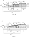
- FIG. 4A is an exemplarily schematic sectional view taken along a line H-H' in FIG. 3
- FIG. 4B is another exemplarily schematic sectional view taken along the line H-H' in FIG. 3
- FIG. 4C is still another exemplarily schematic sectional view taken along the line H-H' in FIG. 3
- FIG. 4D is yet still another exemplarily schematic sectional view taken along the line H-H' in FIG. 3 .
- the substrate 10 includes a base substrate 1 and a common electrode lead 4.
- the base substrate 1 includes a working region 103, a non-working region 101 outside of the working region 103 and an outer profile edge 12. That is, the non-working region 101 is located on a side of the working region 103 near the outer profile edge 12 of the base substrate 1.
- the outer profile edge 12 refers to an outer border of the base substrate 1.
- the non-working region 101 includes a peripheral circuit region 102 near the working region 103 and a non-circuit region away from the working region 103.
- the working region 103 may be a display region or a light-emitting region, etc.
- the non-working region 101 may be a non-display region or a non-light-emitting region, etc.
- the non-working region 101 may have circuits, pads, interconnection structures and so on for supporting and implementing display, light emission and other functions provided therein, although it is not used for display, light emission, etc.
- a circuit layer 2 is provided on the base substrate 1.
- the circuit layer 2 includes a peripheral circuit 13 (the structure of which is not specifically shown in FIG. 4A ) located in the peripheral circuit region 102, for controlling the working state of a working unit within the working region 103.
- the peripheral circuit 13 may be used to control whether the light-emitting unit emits light, or not, and the emitted light intensity.
- the peripheral circuit 13 may, for example, be a driving circuit, such as a gate driving circuit, etc.
- the present embodiment does not limit the type and concrete structure of the peripheral circuit 13.
- the common electrode lead 4 is arranged along the outer profile edge 12 of the base substrate 1.
- the common electrode lead 4 may be arranged along a portion of the outer profile edge 12 of the base substrate 1.
- the orthographic projection of the common electrode lead 4 on the base substrate 1 partially coincides with the orthographic projection of the peripheral circuit region 102 on the base substrate 1.
- a portion of the common electrode lead 4 is located in the peripheral circuit region 102, and the other portion of the common electrode lead 4 is located in a non-circuit region of the non-working region 101.
- the orthographic projection of the common electrode lead 4 on the base substrate 1 partially coincides with the orthographic projection of the peripheral circuit region 102 on the base substrate 1.
- the orthographic projection of the common electrode lead 4 on the base substrate 1 partially coincides with the orthographic projection of the peripheral circuit 13 on the base substrate 1. That is, in a direction perpendicular to the base substrate 1, a portion of the common electrode lead 4 coincides with a portion of the peripheral circuit 13.
- the peripheral circuit 13 includes a plurality of circuit elements (e.g., thin film transistors, lead wires, etc.) and a spacer zone between the plurality of circuit elements, and the orthographic projection of the common electrode lead 4 on the base substrate 1 coincides with the orthographic projection of the spacer zone on the base substrate 1.
- the common electrode lead 4 is insulated from the peripheral circuit 13. Compared with the substrate shown in FIG.
- the width occupied by the common electrode lead 4 alone in the non-working region 101 can be reduced in the substrate 10 provided by an embodiment of the present disclosure, and when the peripheral circuit structure is applied to a substrate, panel or display device, the bezel around a working region can be narrowed (width of the bezel in a direction perpendicular to the common electrode lead is reduced). Or, due to the fact that a portion of the common electrode lead 4 overlaps with a portion of the peripheral circuit 13 and thus that portion of space occupied by the common electrode lead 4 is reduced, it is conducive to increasing the width of the common electrode lead 4, so as to reduce the resistance of the common electrode lead 4.
- the width of the common electrode lead 4 in the embodiment of this disclosure refers to size of a dimension h in a direction perpendicular to the outer profile edge 12 as shown in FIG. 3 .
- the substrate 10 may further include a common electrode 7, which extends from the working region 103 to the peripheral circuit region 102, and is electrically connected to the common electrode lead 4. In this way, a common electrical signal (voltage) is transmitted to the common electrode 7 via the common electrode lead 4, so as to control or drive the working state of the working region 103.
- a common electrical signal voltage
- the substrate 10 may further include a bridging conductive layer 6, which is located in a non-working region 101 (e.g., in a peripheral circuit region 102) and insulated from the peripheral circuit 13.
- the bridging conductive layer 6 extends across the peripheral circuit 13 and electrically connects the common electrode lead 4 with the common electrode 7.
- a portion of the common electrode 7 may be situated in the 3 non-working region 101 and extend from the 3 non-working region 101 to the working region 103.
- One end of the common electrode 7 away from the working region 103 is electrically connected to the bridging conductive layer 6.
- one end of the common electrode 7 away from the working region 103 may be in direct contact with one end of the bridging conductive layer 6 near the working region 103 so as to achieve electrical connection. That is, the common electrode 7 directly overlaps with the bridging conductive layer 6 so as to realize electrical connection between the common electrode 7 and the bridging conductive layer 6.
- the bridging conductive layer 6 is electrically connected to the common electrode lead 4, so as to electrically connect the common electrode lead 4 to the common electrode 7 by the bridging conductive layer 6.
- one end of the bridging conductive layer 6 away from the working region 103 directly overlaps with the common electrode lead 4, so as to achieve electrical connection between the bridging conductive layer 6 and the common electrode lead 4.
- the common electrode 7 may be formed by chemical vapor deposition or magnetron sputtering, or the like
- the bridging conductive layer 6 may be formed by photolithography, while the dimensional accuracy of a film layer formed by chemical vapor deposition or magnetron sputtering is lower than that of a photolithography process, and it generally need to reserve a sufficient packaging space previously in a place of the non-working region 101 on the periphery of a substrate that is near the outer profile edge 12 of the base substrate 1. If the common electrode 7 is made to directly overlap with the common electrode lead 4, it needs more packaging space to be reserved previously. By provision of the bridging conductive layer, the dimensional accuracy in the case that a packaging space is reserved previously can be improved. In this way, it is further conducive to the realization of narrower bezel.
- the common electrode lead 4 may also be arranged along a portion of the outer profile edge 12 of the base substrate 1.
- the orthographic projection of the common electrode lead 4 on the base substrate 1 partially coincides with the orthographic projection of the peripheral circuit region 102 on the base substrate 1, and this is also beneficial to the reduction of the width of the bridging conductive layer 6, so as to beneficial to reducing the resistance of the bridging conductive layer 6.
- the width of the bridging conductive layer 6 refers to the width of the bridging conductive layer 6 in a direction where the above dimension h lies.
- the bridging conductive layer 6, the common electrode lead 4 and the common electrode 7 include material, which is a transparent conductive material, or an opaque conductive material, and the transparent conductive material, for example, may be indium tin oxide (ITO), indium zinc oxide (IZO), or the like, and the opaque conductive material, for example, may be a metallic material, such as copper, aluminum, a copper alloy, an aluminum alloy, or the like, with higher conductivity.
- the bridging conductive layer 6 and common electrode lead 4 adopt the above materials or materials of other kinds with higher conductivity, and this is beneficial to the improvement of the transmission speed of a common signal.
- the working region 103 is a light-emitting region, and light needs to exit from the common electrode 7 side in FIG. 4A
- the common electrode 7 made of a transparent material.
- the peripheral circuit 13 may include an external connection portion 9, and the external connection portion 9 includes an external connection joint 901 and an external connection lead 902.
- the peripheral circuit 13 may include an internal connection portion and the external connection portion 9.
- the internal connection portion refers to a conductive structure and so on formed by interconnection of various components of the peripheral circuit 13.
- the peripheral circuit 13 is a driving circuit, such as a gate driving circuit, or a data driving circuit. Exemplary description will be made below by taking the peripheral circuit 13 being a gate driving circuit as an example, and the gate driving circuit is of GOA type.
- the internal connection portion includes leads inside each driving unit of the gate driving circuit, leads between driving units, and interconnection parts between thin film transistors and capacitors.
- the external connection portion 9 includes a portion of the peripheral circuit 13 connected to its external signal transmission structure.
- the external connection portion 9 includes an external connection joint 901 connected to a plurality of drive units of a gate driving circuit and an external connection lead 902, and the external connection lead 902 can be used to electrically connect the external connection joint 901 with the external signal transmission structure.
- the external connection portion 9 may be used for connection to a timing controller.
- the orthographic projection of the external connection joint 901 on the base substrate 1 does not coincide with the orthographic projection of the common electrode lead 4 on the base substrate 1.
- the peripheral circuit region 102 includes a first zone 1021 away from the working region 103 and a second zone 1022 near the working region.
- the external connection joint 901 is arranged in the second zone 1022 of the peripheral circuit region 102.
- the second zone 1022 does not overlap with the common electrode lead 4 in a direction perpendicular to the base substrate 1, so that the orthographic projection of the external connection joint 901 on the base substrate 1 does not coincide with the orthographic projection of the common electrode lead 4 on the base substrate 1. In this way, it is convenient to form a via hole over the external connection joint 901 and to arrange the external connection lead 902, so that this process will not be hindered by the common electrode lead 4.
- the substrate 10 may further include an interlayer insulating layer 3 arranged between the peripheral circuit 13 and the common electrode lead 4, and the interlayer insulating layer 3 covers the peripheral circuit 13 so that the peripheral circuit 13 is insulated from the common electrode lead 4.
- material of the interlayer insulating layer 3 may be an organic insulating material, such as resin, and rubber, and may also be an inorganic insulating material, such as silicon nitride. Material of the interlayer insulating layer 3 is not limited to the above listed types, and embodiments of the present disclosure do not limit them.
- the interlayer insulating layer 3 includes a via hole exposing the external connection joint 901 of the peripheral circuit 13, through which the external connection lead 902 is electrically connected to the external connection joint 901 of the peripheral circuit 13.
- the external connection lead 902 may be electrically connected to an external controller, such as a timing controller, so that the external controller and the peripheral circuit can be used for joint control of the working state of the working region 103, for example, for control of the turn-on and turn-off of work units of the work region 103, execution of progressive scanning, and so on.
- the external connection lead 902 may be of a same material and arranged in a same layer as the common electrode lead 4. This is conducive to simplifying the structure and simplifying the manufacturing process. Material of the external connection lead 902 may refer to the previous description about the material of the common electrode lead 4.
- the external connection lead and the common electrode lead being arranged in the same layer refers to that the external connection lead and the common electrode lead may be formed by a same patterning process with the same mask, and the external connection lead and the common electrode lead are in contact with a same layer.
- the external connection lead 902 and the common electrode lead 4 contact the interlayer insulating layer 3.
- the substrate 10 may further include a planarization layer 5 covering the peripheral circuit 13 and a portion of the common electrode lead 4, for providing a flat surface for arrangement of functional devices in the working region 103 while insulation of the external connection portion 9 of the peripheral circuit 13 from the bridging conductive layer 6 and the common electrode 7 located above the planarization layer is achieved.
- the planarization layer 5 exposes a portion of the common electrode lead 4, so that the bridging conductive layer 6 can be electrically connected to the common electrode lead 4.
- the interlayer insulating layer 3 has a flat surface on a side near the outer profile edge of the base substrate 1, and in this case, the common electrode lead 4 is arranged on the flat surface.
- the above embodiment is the case where a portion of the common electrode lead 4 overlaps with the first zone 1021 of the peripheral circuit region 102 in a direction perpendicular to the base substrate 1, and in another embodiment of the present disclosure, as shown in FIG. 4C , the entire common electrode lead 4 overlaps with the peripheral circuit 13 in a direction perpendicular to the base substrate 1. That is, the orthographic projection of the common electrode lead 4 on the base substrate 1 falls within the orthographic projection of the peripheral circuit 13 on the base substrate 1. In this way, width of the non-working region 101 can be further reduced, and the bezel width of a device, to which the substrate's peripheral circuit structure 10 is applied, such as a display device, is further reduced.
- the common electrode 7 and the bridging conductive layer 6 may also be an integral structure to realize electrical connection between the common electrode 7 and the common electrode lead 4. It can be understood that the common electrode 7 and the common electrode lead 4 may overlap directly to realize electrical connection between them, while no bridging conductive layer 6 is provided.
- the external connection joint 901 is disposed on a side of the common electrode lead 4 away from the outer profile edge 12 of the base substrate 1.
- an external connection joint may also be located on a side of a common electrode lead near the outer profile edge of a base substrate.
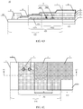
- FIG. 4E is a schematic plan view illustrating another substrate's peripheral circuit structure provided by an embodiment of the present disclosure
- FIG. 4F is a schematically sectional view taken along a line G-G' in FIG. 4E .
- an external connection joint 901 is disposed on a side of a common electrode lead 4 near the outer profile edge of a base substrate 1, that is, the connection joint 901 is disposed between the common electrode lead 4 and the outer profile edge of the base substrate 1.
- the length of the bridging conductive layer 6 can be further reduced by the embodiment shown in FIG.4F , and the resistance of the bridging conductive layer 6 is further reduced.
- Other technical effects brought about by the embodiment shown in FIG. 4F can refer to the above descriptions, and no details are repeated here.
- FIG. 4G is a schematically partial enlarged view of a peripheral circuit in FIG. 4A .
- the peripheral circuit 13 may include a plurality of thin film transistors arranged on the base substrate 1, for example, a first thin film transistor 131 and a second thin film transistor 132.
- Each of the first thin film transistor 131 and the second thin film transistor 132 includes a first portion 1301 and a gate electrode 1305.
- a source electrode, a drain electrode, and a channel area are included in each of the first portions 1301 of the first thin film transistor 131 and the second thin film transistor 132.
- the peripheral circuit 13 may further include a first insulating layer 1302 covering the first portions 1301 of the first thin film transistor 131 and the second thin film transistor 132, a capacitor and a peripheral circuit signal output lead 1306.
- the peripheral circuit signal output lead 1306 is configured to output an output signal of the peripheral circuit to the working region on an inner side of the non-working region.
- a gate driving signal (a progressive scanning signal) is outputted from the peripheral circuit signal output lead 1306.
- the capacitor includes a first plate 1304 and a second plate 1310 disposed to be opposed.
- the gate electrode 1305 of thin film transistor, the first plate 1304 of the capacitor and the peripheral circuit signal output lead 1306 are arranged in a same layer, and each of them is disposed on the first insulating layer 1302. They may be made of a same material, and may be formed simultaneously by a same process. For example, they are formed by a same patterning process with a same mask.
- the peripheral circuit may further include a second insulating layer 1307 covering the gate electrode 1305, the first plate 1304 of the capacitor and the peripheral circuit signal output lead 1306.
- the first insulating layer 1302 and the second insulating layer 1307 contain second via holes exposing source electrodes or drain electrodes of the thin film transistors.
- the peripheral circuit 12 further includes an internal connection portion including a connecting line, and for example, the connecting line includes a first portion 1311, a second portion 1312 and a third portion 1313.
- the second plate 1310 of the capacitor, the connecting line and the external connection joint 901 are arranged on the second insulating layer 1307.
- a drain electrode of the first thin film transistor 131 is electrically connected to a source electrode of the second thin film transistor 132 by the second portion 1312 of the connecting line through a second via hole.
- the second plate 1310 of the capacitor is electrically connected to a source electrode of the first thin film transistor 131 by the first portion 1311 of the connecting line through a second via hole.
- the second plate 1310 of the capacitor and the connecting line 1311 may be formed integrally, and they can be formed of a same material simultaneously by a same patterning process with a same mask.
- a drain electrode of the second thin film transistor 132 is electrically connected to the peripheral circuit signal output lead 1306 by the third portion 1313 of the connecting line.
- the external connection joint 901, the second plate 1310 of the capacitor and the connecting line are disposed in a same layer.
- 'being disposed in the same layer' in the present disclosure refers to that structures disposed in the same layer may be formed from the same material simultaneously by the same patterning process with the same mask, and in contact with a same layer, which does not refer to that height of these structures relative to the base substrate is the same.
- the external connection joint 901, the second plate 1310 of the capacitor and the connecting line are made of a same material, and formed from a same film layer simultaneously by a same patterning process with a same mask, and the external connection joint 901, the second plate 1310 of the capacitor and the connecting line are all in contact with the second insulating layer 1307, so as to simplify structure of the peripheral circuit and fabrication process.
- material of the external connection joint 901, the second plate 1310 of the capacitor and the connecting line may be copper, aluminum, a copper alloy, an aluminum alloy, silver, chromium, or the like, but is not limited to the above listed categories.
- Embodiments of the present disclosure do not set a limit to the material of components, and those skilled in the art can make a reference to a common technique.
- the entire peripheral circuit 13 is located below the interlayer insulating layer 3, that is, the interlayer insulating layer 3 covers the peripheral circuit 13.
- the interlayer insulating layer 3 covers the external connection joint 901, the second plate 1310 of the capacitor and the connecting line, etc.
- a flat insulating layer can be formed on the peripheral circuit 13, and when a common electrode lead 4 is arranged on an interlayer insulating layer 3, and the common electrode lead 4 partially or even completely overlaps with a peripheral circuit below the interlayer insulating layer 3, insulation of the common electrode lead 4 from the peripheral circuit 13 can be achieved.
- the substrate provided by an embodiment of the present disclosure may be an array substrate, or a display substrate, etc.
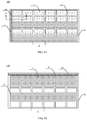
- FIG. 5A is a schematic plan view of an array substrate provided by an embodiment of the present disclosure
- FIG. 5B is a schematic plan view of another array substrate provided by an embodiment of the present disclosure
- FIG. 5C is a schematic plan view of still another array substrate provided by an embodiment of the present disclosure
- FIG. 6 is a schematically sectional view taken along a line G-G' in FIG. 5A .
- a common electrode lead 4 and a peripheral circuit of a peripheral circuit region 102 are used to control the working state of a working region 103.
- the common electrode lead 4 and the peripheral circuit region 102 may be in a place on the left side of an array substrate 100 near its outer profile edge, and a control signal is input from the left side to the working region 103.
- a common electrode lead 4 and a peripheral circuit region 102 may also be arranged in a place on the upper side of an array substrate 100 near its outer profile edge, and a control signal is input from the upper side to a working region 103.
- FIG. 5A a common electrode lead 4 and a peripheral circuit of a peripheral circuit region 102 are used to control the working state of a working region 103.
- the common electrode lead 4 and the peripheral circuit region 102 may be in a place on the left side of an array substrate 100 near its outer profile edge, and a control signal is input from the left side to the working region 103.
- a control signal is input from the upper side to a
- a common electrode lead 4 and a peripheral circuit region 102 may also be arranged in a place on opposite sides of an array substrate 100, such as on the left side and the right side, near its outer profile edge.
- control signals can be input to a working region 103 at two sides at the same time, and a technical effect of reducing signal delay can be achieved.
- a better working effect is achieved by the array substrate 100.
- the planar area of an array substrate 100 is larger, this technical effect is more significant.
- the working region is provided with a display element therein, and the display element includes a pixel defining layer, a light emitting layer, a first electrode and a second electrode.
- the pixel defining layer includes a plurality of openings; the light emitting layer is disposed in the plurality of openings; the first electrode covers the pixel defining layer and the light emitting layer, and extends from the display region toward the first common electrode lead; and the second electrode is arranged between the base substrate and the light emitting layer.
- the first electrode is a common cathode, and the first common electrode lead is a common cathode lead; or the first electrode is a common anode, and the first common electrode lead is a common anode wire.
- the working region 103 is provided with a plurality of array elements 14, and the plurality of array elements include a common electrode 7, and the common electrode 7 is electrically connected to a common electrode lead 4.
- the array elements 14 may be an organic light-emitting diode device, and the organic light-emitting diode device may be a top emission configuration, a bottom emission configuration, or other configuration.
- the organic light-emitting diode device may include an anode 15 arranged on a base substrate 1, a cathode disposed on the base substrate 1 to be opposed to the anode 15, and an organic light-emitting layer 16 arranged between the anode 15 and the cathode. In the embodiment shown in FIG.
- the cathode is a common electrode 7, and in this case, the common electrode lead 4 is a common cathode lead, the first electrode is a cathode (i.e., the common cathode), the second electrode is an anode, and a low-level signal is input to the common electrode 7 during the operation.
- the anode 15 may be a reflective electrode, or a reflective layer (not shown in the figure) is disposed to be adjacent to the anode 15, and lights are exited from the cathode side during operation.
- the cathode may be a reflective electrode, or a reflective layer is provided to be adjacent to the cathode, and lights are exited from the anode side during operation.
- positions of the anode and the cathode are exchangeable.
- the anode may be a common electrode 7.
- the common electrode lead 4 is a common anode lead
- the first electrode is an anode (i.e., the common anode)
- the second electrode is a cathode
- a high-level signal is input to the common electrode 7 during operation.
- the organic light-emitting diode device may further include a pixel defining layer 8 to define a plurality of light-emitting units or pixel units, so that crosstalk between lights from adjacent light-emitting units or adjacent pixel units is prevented.
- the pixel defining layer 8 includes a plurality of openings, the organic light-emitting layer 16 is arranged in the openings, and the common electrode 7 may cover the pixel defining layer 8.
- the perimeter circuit 13 may be a gate driving circuit, or a data driving circuit, etc.
- the gate driving circuit or the data driving circuit includes thin film transistors, capacitors, gate-line leads or data-line leads, etc.
- the array substrate provided by an embodiment of the disclosure can be used for electronic devices, such as display devices, illuminating devices, or the like.
- width occupied by the common electrode lead 4 alone in the non-working region 101 is reduced, so that the array substrate has a narrower bezel.
- a narrower bezel can be realized by a display device, an illuminating device, or the like, which adopt the array substrate.
- a narrower bezel can be realized by a display device, an illuminating device, or the like, which adopt the array substrate.
- the saved space can be used to increase width of a common electrode lead, so as to reduce the resistance of the common electrode lead.
- the resistance of the common electrode lead can be reduced.
- it is propitious for the improvement of the transmission speed of a signal in the common electrode lead in addition, it is helpful to reducing the power consumption and the generated Joule heat of the common electrode lead during the operation, and to reducing temperature rise caused by the Joule heat. Consequently, it is beneficial to the improvement of the lifetime of the array substrate, the display device, or the illuminating device.
- FIG. 7 is a schematic diagram of a display device provided by an embodiment of the present disclosure.
- the display device includes any of the array substrates provided by the embodiments of the present disclosure.
- the display device may be an organic light-emitting diode display device.
- the display device may be implemented as the following products: a mobile phone, a tablet computer, a television, a display, a notebook computer, a digital photo frame, a navigator, or any other product or component with display function.
- FIG. 7 is only a schematic diagram of a display device that includes any of the array substrates provided in embodiment 2.
- FIG. 7 is only a schematic diagram of a display device that includes any of the array substrates provided in embodiment 2.
- FIG. 7 reference can be made to conventional techniques by those skilled in the art, and embodiments of the present disclosure do not limit them.
- a narrower bezel can be achieved by the display device provided by an embodiment of the present disclosure. While a narrow bezel is realized, it is also beneficial to increasing width of a common electrode lead, so as to reduce the resistance of the common electrode lead. In this way, the resistance of the common electrode lead can be reduced. On the one hand, it is propitious for the improvement of the transmission speed of signal in the common electrode lead, in addition, it is beneficial to reducing power consumption and the generated joule heat of the common electrode lead during operation, to reducing the temperature rise caused by the Joule heat. Consequently, it is beneficial to the improvement of the lifetime of an array substrate, a display device, or an illuminating device.
- At least one embodiment of the present disclosure also provides an array substrate manufacturing method, including: providing a base substrate including a working region, a non-working region outside of the working region and an outer profile edge, the non-working region including a peripheral circuit region near the working region and a non-circuit region away from the working region; a peripheral circuit is formed in the peripheral circuit region of the non-working region; and a common electrode lead extending along at least part of the outer profile edge of the base substrate is formed.
- the peripheral circuit region is provided with the peripheral circuit, the peripheral circuit is not provided in the non-circuit region, the orthographic projection of the common electrode lead on the base substrate at least partially coincides with the orthographic projection of the peripheral circuit region on the base substrate, and the common electrode lead is insulated from the peripheral circuit.
- FIGs. 8A to 8M are schematic diagrams illustrating an array substrate manufacturing method provided by an embodiment of the present disclosure.
- An exemplary introduction will be given below with reference to an example in which an array substrate with an organic light-emitting diode (OLED) device being included in a working region is formed.
- OLED organic light-emitting diode
- a base substrate 1 is provided.
- the base substrate 1 may be, for example, a glass substrate, a quartz substrate, a resin (e.g. polyethylene) substrate, etc.
- the base substrate 1 has an outer profile edge 12 and includes a working region 103 and a non-working region 101 outside of the working region 103.
- the non-working region 101 includes a peripheral circuit region 102 near the working region 103.
- a circuit layer 2 is formed on the base substrate 1, which includes forming a peripheral circuit 13 in the peripheral circuit region 102.
- the peripheral circuit 13 may, for example, be a driving circuit, such as a gate driving circuit, or a data driving circuit. The manufacturing method of the circuit will be exemplarily introduced below by taking the peripheral circuit 13 being a gate driving circuit as an example.
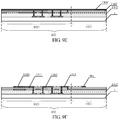
- FIGs. 9A to 9F are schematic diagrams illustrating a manufacturing method of the driving circuit.
- Forming the peripheral circuit 13 includes forming an internal connection portion and an external connection portion of the peripheral circuit 13.
- the external connection portion includes an external connection joint and an external connection lead, and the orthographic projection of the external connection joint on the base substrate 1 does not coincide with the orthographic projection of a common electrode lead 4 on the base substrate 1.
- the peripheral circuit region 102 includes a first zone 1021 away from the working region 103 and a second zone 1022 near the working region 103.
- the internal connection portion is disposed in the first zone 1021 of the peripheral circuit region 102, and the external connection joint is formed within the second zone 1022 of the peripheral circuit region 102.
- the first zone 1021 does not coincide with the common electrode lead 4 in a direction perpendicular to the base substrate 1, so that the orthographic projection of the external connection joint on the base substrate 1 does not coincide with the orthographic projection of the common electrode lead 4 on the base substrate 1.
- Forming the peripheral circuit includes forming a plurality of thin film transistors, such as forming a first thin film transistor and a second thin film transistor.
- a gate electrode, a source electrode, and a drain electrode are included in each of the first thin film transistor and the second thin film transistor.
- a first portion 1301 includes a channel area, a source area, and a drain area.
- a gate metal layer 1303 is formed on the first insulating layer 1302, and for example, the gate metal layer 1303 may be formed by chemical vapor deposition, magnetron sputtering, or the like.
- Material of the gate metal layer 1303 may be copper, aluminum, a copper alloy, an aluminum alloy, silver, chromium, or the like, but is not limited to the above listed categories.
- Forming the peripheral circuit includes forming a gate-metal-layer pattern. For example, it may include forming gate electrodes of a plurality of thin film transistors, a first plate of a capacitor, a pattern of a connecting line between the gate electrodes of the plurality of thin film transistors and a pattern of a peripheral circuit output lead by a same patterning process with a same mask.
- the gate metal layer 1303 is patterned, to simultaneously form a pattern of a plurality of gate electrodes 1305 corresponding to first portions 1301 of the plurality of thin film transistors, respectively, the first plate 1304 of the capacitor, the plurality of gate electrodes 1305 and a peripheral circuit signal output lead 1306.
- the patterning can be realized by a photolithographic process.
- a second insulating layer 1307 covering a pattern formed by a gate metal layer 1303.
- Second via holes 1308 for exposing source electrodes and drain electrodes of a plurality of thin film transistors that are located in the first insulating layer 1302 and the second insulating layer 1307 are formed.
- material of the first insulating layer 1302 and the second insulating layer 1307 may be an inorganic insulating material, such as silicon nitride, etc.
- the second via holes 1308 may be formed by a photolithographic process including exposure, development and etching.
- material of the first insulating layer 1302 and the second insulating layer 1307 may be an inorganic insulating material or an organic insulating material, which may, for example, be a photosensitive organic insulating material.
- the second via holes 1308 may be formed by exposure-development process. In this way, the etching steps can be decreased, and the process can be simplified.
- the method further includes forming a second-metal-layer pattern, which may include forming a second plate of a capacitor, a connecting line of the peripheral circuit, and the external connection joint by a same patterning process with a same mask.
- the connecting line includes a first portion, a second portion and a third portion.
- the second plate of the capacitor is electrically connected to a source electrode of the first thin film transistor by the first portion of the connecting line.
- a drain electrode of the first thin film transistor is electrically connected with a source electrode of the second thin film transistor by the second portion of the connecting line.
- a drain electrode of the second thin film transistor is electrically connected with the peripheral circuit signal output lead by the third portion of the connecting line.
- a second metal layer 1309 is formed on the second insulating layer 1307, and the second metal layer 1309 is electrically connected to the source areas and drain areas of active layers of the thin film transistors through the second via holes 1308.
- the second metal layer 1309 may be formed by chemical vapor deposition, magnetron sputtering, or the like.
- Material of the second metal layer 1309 may be copper, aluminum, a copper alloy, an aluminum alloy, silver, chromium, or the like, but is not limited thereto.
- the second metal layer 1309 is patterned to simultaneously form a pattern of a second plate 1310 of a capacitor, a first portion 1311 of a connecting line for electrically connecting the second plate 1310 of the capacitor to a source electrode of the first thin film transistor, a second portion 1312 of the connection line that electrically connects a drain electrode of the first thin film transistor to a source electrode of the second thin film transistor, a third portion 1313 of the connecting line for electrically connecting a drain electrode of the second thin film transistor to the peripheral circuit signal output lead 1306 and an external connection joint 901.
- locating the external connection joint 901 in the second zone 1022 may be realized in the process of patterning the second metal layer 1309. For example, it may be electrically connected to source electrodes or drain electrodes of a plurality of thin film transistors in each row. It may also be used for connection to a controller outside of the gate driving circuit 13, for example, it may be connected to a timing controller, or the like.
- the external connection joint 901 is disposed in the second zone 1022 of the peripheral circuit region 102, so as to make preparation for the subsequent formation of an external connection portion of the peripheral circuit in the second zone 1022.
- the method provided by an embodiment of the present disclosure it is possible that after a part of devices (such as a second plate of a capacitor and an external connection joint) of the peripheral circuit and connection pattern between devices are simultaneously formed with the second metal layer 1309, it is unnecessary to separately form a metal used to connect the devices after formation of devices of the peripheral circuit, which is beneficial to the simplification of the process.
- number/amount of the external connection joints 901 shown in FIG. 9F is one, which is merely acts as an exemplary description, and amount of the external connection joints 901 maybe multiple.
- the method further includes forming an interlayer insulating layer 3 on the peripheral circuit layer 2.
- the whole peripheral circuit 13 is disposed below the interlayer insulating layer 3, that is, the interlayer insulating layer 3 covers the peripheral circuit 13.
- the interlayer insulating layer 3 covers the external connection joint 901, the second plate 1310 of the capacitor, and the connecting line, etc. In this way, a flat insulating layer can be formed on the peripheral circuit 13.
- a common electrode lead 4 is arranged on the interlayer insulating layer 3, and a portion or even the entirety of the common electrode lead 4 overlaps with the peripheral circuit under the interlayer insulating layer 3, the insulation of the common electrode lead 4 from the peripheral circuit 13 can be realized.
- Material of the interlayer insulating layer 3 may be the same as that of the first insulating layer 1302, which can refer to the above description.
- the interlayer insulating layer 3 may be formed by a coating process, a deposition process, or the like.
- a via hole 301 exposing the external connection joint 901 is formed in the interlayer insulating layer 3.
- the specific method may refer to the above description about the method for forming the second via hole 1308.
- a common electrode lead layer 901 is formed on the interlayer insulating layer 3.
- Material of the common electrode lead layer 901 may, for example, be a transparent conductive material or an opaque conductive material.
- the transparent conductive material may be material, such as indium tin oxide (ITO), indium zinc oxide (IZO), or the like, and the opaque conductive material may, for example, be a metallic material, such as copper, aluminum, a copper alloy, or the like, with higher conductivity.
- the common electrode lead layer 901 may be formed by chemical vapor deposition, magnetron sputtering, or the like.
- the common electrode lead layer 901 may be patterned by a photolithographic process so as to form a common electrode lead 4 along at least part of the outer profile edge of the base substrate 1.
- the orthographic projection of the common electrode lead 4 on the base substrate 1 coincides with a portion of the projection of an internal connected portion of the peripheral circuit 13 in the peripheral circuit region 102 on the base substrate 1, that is, it overlaps with the internal connection portion of the peripheral circuit in the peripheral circuit region 102 in a direction perpendicular to the base substrate 1.
- the width area occupied by the common electrode lead 4 alone in the non-working region 101 can be reduced in the array substrate obtained by using the method provided by an embodiment of the present disclosure, and the array substrate can have a narrower bezel.
- a narrower bezel can be achieved by a display device, an illuminating device, or the like, which adopt the array substrate.
- the saved space may be used to increase the width of a common electrode lead, so as to reduce the resistance of the common electrode lead.
- the interlayer insulating layer 3 is arranged between the peripheral circuit 13 and the common electrode lead 4, and covers the peripheral circuit 13, so that the peripheral circuit 13 and the common electrode lead 4 are insulated from each other.
- the external connection portion 9 of the peripheral circuit 13 includes an external connection joint 901 and an external connection lead 902.
- the external connection lead 902 is formed while the common electrode lead 4 is formed by patterning the common electrode lead layer 901, namely the external connection lead 902 of the peripheral circuit 13 and the common electrode lead 4 are formed by a same patterning process with a same mask. In this way, it is beneficial to the simplification of the fabricating process of the array substrate.
- the external connection lead 902 is electrically connected to the external connection joint 901 through the via hole 301.
- the external connection joint 901 is formed in a second zone 1022 of the peripheral circuit region that does not overlap with the common electrode lead 4 in a direction perpendicular to the base substrate 1, so as to facilitate forming a via hole over the external connection joint 901 and arranging the external connection lead 902. In this way, this process will not be hindered by the common electrode lead 4.
- planarization layer 5 covering the base substrate 1 is formed.
- the specific formation method and material of the planarization layer 5 may refer to conventional techniques in the field.
- the planarization layer 5 is patterned to form an opening that exposes at least part of the common electrode lead 4.
- a pixel defining layer 8 is formed on the planarization layer 5 by photolithography.
- the pixel defining layer 8 has an opening.
- a conductive layer 602 is formed on the planarization layer 5.
- Material of the conductive layer 602 may be a transparent conductive material, or an opaque conductive material.
- the transparent conductive material may be material, such as indium tin oxide (ITO), or indium zinc oxide (IZO), or the like
- the opaque conductive material may, for example, be a metallic material, such as copper, aluminum, a copper alloy, an aluminum alloy, or the like.
- the conductive layer 602 may be formed by chemical vapor deposition, magnetron sputtering, or the like. It is to be noted that material and specific production method of the conductive layer 602 are not limited to the above listed categories.
- the conductive layer 602 may be patterned by photolithography, to form a bridging conductive layer 6 and an anode 15 simultaneously.
- the anode 15 formed in FIG. 8J may also be changed to be a cathode.
- the anode 15 is located in the working region 103, and in an opening of the pixel defining layer 8.
- the bridging conductive layer 6 is formed in the peripheral circuit region 102, and is insulated from the peripheral circuit 13 and extends across the peripheral circuit 13.
- the bridging conductive layer 6 is electrically connected with the common electrode lead 4. In the embodiment shown in FIGs.
- one end of the bridging conductive layer 6 away from the working region 103 directly overlaps with the common electrode lead 4 to achieve electrical connection between the two.
- This direct overlapping is beneficial to the reduction of the contact resistance and is easy to be fabricated.
- the orthographic projection of the common electrode lead 4 on the base substrate 1 partially coincides with the orthographic projection of the peripheral circuit region 102 on the base substrate 1.
- the orthographic projection of the common electrode lead 4 on the base substrate 1 partially coincides with the orthographic projection of the peripheral circuit 13 on the base substrate 1. That is, in a direction perpendicular to the base substrate 1, a portion of the common electrode lead 4 coincides with a portion of the peripheral circuit 12.
- the peripheral circuit 13 includes a plurality of circuit elements (such as thin film transistors, and leads, etc.) and a spacer zone interposed between the plurality of circuit elements, and the orthographic projection of the common electrode lead 4 on the base substrate 1 coincides with the orthographic projection of the spacer zone on the base substrate 1.
- circuit elements such as thin film transistors, and leads, etc.
- an organic light-emitting layer 16 may be formed on the anode 15 by a coating process or a deposition process. In other embodiment, it may be an electroluminescent layer (e.g., an organic electroluminescent layer).
- a common electrode 7 is formed in the working region 103.
- the common electrode 7 may on the organic light-emitting layer 16 and the pixel defining layer 8, and extend to the peripheral circuit region 102 and directly contact the bridging conductive layer 6 to achieve electrical connection between them.
- electrical connection between the common electrode 7 and the common electrode lead 4 is achieved through the bridging conductive layer 6. That is, the bridging conductive layer 6 electrically connects the common electrode lead 4 with the common electrode 7.
- An array substrate 100 as shown in FIG. 8L can be formed by the above method.
- FIG. 8M is an enlarged schematic diagram of part 20 of the array substrate 100 in FIG. 8L .
- the enlarged schematic diagram exemplarily illustrates structure of the peripheral circuit 13.
- Embodiments of the present disclosure provide a display-substrate peripheral circuit structure, an array substrate and a method of manufacturing the same, and a display device, in which, a common electrode lead at least partially overlaps with and is insulated from a peripheral circuit region, so that the width area occupied by the common electrode lead alone in a non-working region can be reduced, and when the peripheral circuit structure is applied to the display device and so on, it is beneficial to the realization of a narrower bezel.
Landscapes
- Engineering & Computer Science (AREA)
- Microelectronics & Electronic Packaging (AREA)
- Devices For Indicating Variable Information By Combining Individual Elements (AREA)
- Electroluminescent Light Sources (AREA)
Applications Claiming Priority (2)
| Application Number | Priority Date | Filing Date | Title |
|---|---|---|---|
| CN201711376371.XA CN109935580B (zh) | 2017-12-19 | 2017-12-19 | 基板及其制作方法、电子装置 |
| PCT/CN2018/121508 WO2019120168A1 (zh) | 2017-12-19 | 2018-12-17 | 基板及其制作方法、电子装置 |
Publications (3)
| Publication Number | Publication Date |
|---|---|
| EP3731279A1 true EP3731279A1 (de) | 2020-10-28 |
| EP3731279A4 EP3731279A4 (de) | 2021-09-15 |
| EP3731279B1 EP3731279B1 (de) | 2025-08-20 |
Family
ID=66983834
Family Applications (1)
| Application Number | Title | Priority Date | Filing Date |
|---|---|---|---|
| EP18893149.7A Active EP3731279B1 (de) | 2017-12-19 | 2018-12-17 | Substrat und herstellungsverfahren dafür und elektronische vorrichtung |
Country Status (4)
| Country | Link |
|---|---|
| US (2) | US10943957B2 (de) |
| EP (1) | EP3731279B1 (de) |
| CN (2) | CN109935580B (de) |
| WO (1) | WO2019120168A1 (de) |
Families Citing this family (6)
| Publication number | Priority date | Publication date | Assignee | Title |
|---|---|---|---|---|
| CN109545835B (zh) * | 2018-12-13 | 2021-02-09 | 京东方科技集团股份有限公司 | 显示基板及其制备方法、显示装置 |
| CN111863910B (zh) * | 2020-07-28 | 2023-11-17 | 京东方科技集团股份有限公司 | 显示基板及其制备方法、显示装置 |
| CN112736095B (zh) * | 2021-01-15 | 2025-12-16 | 武汉华星光电技术有限公司 | 显示面板 |
| CN113066849B (zh) * | 2021-03-31 | 2023-05-02 | 京东方科技集团股份有限公司 | 显示面板和显示装置 |
| CN115472626A (zh) * | 2021-05-24 | 2022-12-13 | 京东方科技集团股份有限公司 | 显示基板及其制作方法、显示装置 |
| CN115079864B (zh) * | 2022-06-14 | 2025-04-04 | 京东方科技集团股份有限公司 | 一种显示面板及显示装置 |
Family Cites Families (24)
| Publication number | Priority date | Publication date | Assignee | Title |
|---|---|---|---|---|
| US7095460B2 (en) * | 2001-02-26 | 2006-08-22 | Samsung Electronics Co., Ltd. | Thin film transistor array substrate using low dielectric insulating layer and method of fabricating the same |
| KR100796749B1 (ko) * | 2001-05-16 | 2008-01-22 | 삼성전자주식회사 | 액정 표시 장치용 박막 트랜지스터 어레이 기판 |
| WO2006126304A1 (ja) * | 2005-05-25 | 2006-11-30 | Sharp Kabushiki Kaisha | 発光回路基板及び発光表示装置 |
| KR100716283B1 (ko) * | 2006-08-11 | 2007-05-09 | 삼성전자주식회사 | 표시장치 |
| CN101494201B (zh) | 2008-01-25 | 2010-11-03 | 北京京东方光电科技有限公司 | 薄膜晶体管液晶显示器阵列基板结构及其制造方法 |
| KR101769068B1 (ko) * | 2010-12-14 | 2017-08-18 | 삼성디스플레이 주식회사 | 유기 발광 표시 장치 |
| US9478598B2 (en) * | 2011-11-07 | 2016-10-25 | Joled Inc. | Organic electroluminescence display panel and organic electroluminescence display apparatus |
| KR101295536B1 (ko) | 2012-03-26 | 2013-08-12 | 엘지디스플레이 주식회사 | 터치 스크린 일체형 표시장치 및 그 제조 방법 |
| TWI514055B (zh) * | 2013-05-16 | 2015-12-21 | Au Optronics Corp | 顯示面板與其製造方法 |
| JP6188473B2 (ja) | 2013-07-31 | 2017-08-30 | 三菱電機株式会社 | 薄膜トランジスタアレイ基板およびその製造方法 |
| KR102117109B1 (ko) * | 2013-10-22 | 2020-06-01 | 삼성디스플레이 주식회사 | 유기 발광 표시 장치 |
| KR102282996B1 (ko) * | 2013-10-30 | 2021-07-29 | 삼성디스플레이 주식회사 | 유기 발광 표시 장치 및 그의 제조 방법 |
| CN104485349B (zh) | 2014-12-26 | 2017-08-25 | 昆山工研院新型平板显示技术中心有限公司 | 无边框显示屏器件 |
| CN104576659A (zh) * | 2015-02-09 | 2015-04-29 | 京东方科技集团股份有限公司 | 一种阵列基板及其制作方法、显示装置 |
| KR102336419B1 (ko) * | 2015-04-30 | 2021-12-06 | 엘지디스플레이 주식회사 | 액정 표시 장치용 어레이 기판 |
| KR102393931B1 (ko) * | 2015-05-01 | 2022-05-04 | 삼성디스플레이 주식회사 | 유기 발광 표시 장치 |
| CN104777637B (zh) | 2015-05-08 | 2018-01-02 | 上海中航光电子有限公司 | 阵列基板、触控显示装置及其测试方法 |
| US10114258B2 (en) | 2015-05-31 | 2018-10-30 | Lg Display Co., Ltd. | Narrow bezel display device |
| KR102419179B1 (ko) * | 2015-09-11 | 2022-07-11 | 삼성디스플레이 주식회사 | 유기 발광 표시 장치 |
| CN105244365B (zh) | 2015-11-18 | 2018-09-25 | 上海天马有机发光显示技术有限公司 | 显示装置、制造方法及显示设备 |
| CN105807523B (zh) * | 2016-05-27 | 2020-03-20 | 厦门天马微电子有限公司 | 阵列基板、包含其的显示面板和显示装置 |
| CN107452780B (zh) * | 2017-07-31 | 2020-05-19 | 京东方科技集团股份有限公司 | Oled基板及制作方法、显示装置 |
| CN107390941B (zh) * | 2017-08-17 | 2021-01-29 | 京东方科技集团股份有限公司 | 触控基板、触控面板、显示基板、显示面板和显示装置 |
| CN207517696U (zh) | 2017-12-19 | 2018-06-19 | 京东方科技集团股份有限公司 | 基板及电子装置 |
-
2017
- 2017-12-19 CN CN201711376371.XA patent/CN109935580B/zh active Active
- 2017-12-19 CN CN202411965318.3A patent/CN119653997A/zh active Pending
-
2018
- 2018-12-17 EP EP18893149.7A patent/EP3731279B1/de active Active
- 2018-12-17 WO PCT/CN2018/121508 patent/WO2019120168A1/zh not_active Ceased
- 2018-12-17 US US16/481,482 patent/US10943957B2/en active Active
-
2021
- 2021-02-08 US US17/170,437 patent/US11417713B2/en active Active
Also Published As
| Publication number | Publication date |
|---|---|
| CN109935580A (zh) | 2019-06-25 |
| WO2019120168A1 (zh) | 2019-06-27 |
| EP3731279B1 (de) | 2025-08-20 |
| US10943957B2 (en) | 2021-03-09 |
| US20190348479A1 (en) | 2019-11-14 |
| US20210167142A1 (en) | 2021-06-03 |
| US11417713B2 (en) | 2022-08-16 |
| CN119653997A (zh) | 2025-03-18 |
| EP3731279A4 (de) | 2021-09-15 |
| CN109935580B (zh) | 2025-01-17 |
Similar Documents
| Publication | Publication Date | Title |
|---|---|---|
| US11417713B2 (en) | Substrate and manufacturing method therefor, and electronic apparatus | |
| US8487313B2 (en) | Emissive device and electronic apparatus | |
| CN115835687B (zh) | 一种显示面板和显示装置 | |
| CN110416226B (zh) | 一种显示面板及其制作方法和显示装置 | |
| KR20120042438A (ko) | 터치인식 유기전계 발광소자 | |
| JP7368233B2 (ja) | 基板及びその製造方法、電子装置 | |
| CN114927548A (zh) | 一种显示面板和显示装置 | |
| KR20230103248A (ko) | 표시 장치 | |
| KR20220161618A (ko) | 표시 장치 및 표시 장치의 제조 방법 | |
| CN115210880A (zh) | 显示基板及其制作方法、显示装置 | |
| CN207517696U (zh) | 基板及电子装置 | |
| KR20160090233A (ko) | 디스플레이 디바이스 | |
| JP2021026099A (ja) | 表示装置 | |
| CN115955880A (zh) | 显示面板和显示装置 | |
| JP2007156388A (ja) | 発光装置および電子機器 | |
| US20240397780A1 (en) | Display substrate and display device | |
| US12414419B2 (en) | Display substrate | |
| CN117794292A (zh) | 显示面板和显示装置 | |
| CN120897639A (zh) | 显示面板及显示终端 | |
| KR20240114316A (ko) | 표시 장치 | |
| CN115915853A (zh) | 一种显示面板及显示装置 | |
| CN115275059A (zh) | 一种显示面板和显示装置 |
Legal Events
| Date | Code | Title | Description |
|---|---|---|---|
| STAA | Information on the status of an ep patent application or granted ep patent |
Free format text: STATUS: THE INTERNATIONAL PUBLICATION HAS BEEN MADE |
|
| PUAI | Public reference made under article 153(3) epc to a published international application that has entered the european phase |
Free format text: ORIGINAL CODE: 0009012 |
|
| STAA | Information on the status of an ep patent application or granted ep patent |
Free format text: STATUS: REQUEST FOR EXAMINATION WAS MADE |
|
| 17P | Request for examination filed |
Effective date: 20190730 |
|
| AK | Designated contracting states |
Kind code of ref document: A1 Designated state(s): AL AT BE BG CH CY CZ DE DK EE ES FI FR GB GR HR HU IE IS IT LI LT LU LV MC MK MT NL NO PL PT RO RS SE SI SK SM TR |
|
| AX | Request for extension of the european patent |
Extension state: BA ME |
|
| DAV | Request for validation of the european patent (deleted) | ||
| DAX | Request for extension of the european patent (deleted) | ||
| A4 | Supplementary search report drawn up and despatched |
Effective date: 20210816 |
|
| RIC1 | Information provided on ipc code assigned before grant |
Ipc: H01L 27/02 20060101ALI20210810BHEP Ipc: H01L 27/32 20060101AFI20210810BHEP |
|
| P01 | Opt-out of the competence of the unified patent court (upc) registered |
Effective date: 20230527 |
|
| REG | Reference to a national code |
Ref legal event code: R079 Free format text: PREVIOUS MAIN CLASS: H01L0027320000 Ipc: H10D0086400000 Ref country code: DE Ref document number: 602018084847 Country of ref document: DE |
|
| GRAP | Despatch of communication of intention to grant a patent |
Free format text: ORIGINAL CODE: EPIDOSNIGR1 |
|
| STAA | Information on the status of an ep patent application or granted ep patent |
Free format text: STATUS: GRANT OF PATENT IS INTENDED |
|
| RIC1 | Information provided on ipc code assigned before grant |
Ipc: H10K 59/131 20230101ALI20250210BHEP Ipc: H10D 86/60 20250101ALI20250210BHEP Ipc: H10D 86/40 20250101AFI20250210BHEP |
|
| INTG | Intention to grant announced |
Effective date: 20250314 |
|
| GRAS | Grant fee paid |
Free format text: ORIGINAL CODE: EPIDOSNIGR3 |
|
| GRAA | (expected) grant |
Free format text: ORIGINAL CODE: 0009210 |
|
| STAA | Information on the status of an ep patent application or granted ep patent |
Free format text: STATUS: THE PATENT HAS BEEN GRANTED |
|
| AK | Designated contracting states |
Kind code of ref document: B1 Designated state(s): AL AT BE BG CH CY CZ DE DK EE ES FI FR GB GR HR HU IE IS IT LI LT LU LV MC MK MT NL NO PL PT RO RS SE SI SK SM TR |
|
| REG | Reference to a national code |
Ref country code: GB Ref legal event code: FG4D |
|
| REG | Reference to a national code |
Ref country code: CH Ref legal event code: EP |
|
| REG | Reference to a national code |
Ref country code: IE Ref legal event code: FG4D |
|
| REG | Reference to a national code |
Ref country code: DE Ref legal event code: R096 Ref document number: 602018084847 Country of ref document: DE |
|
| REG | Reference to a national code |
Ref country code: NL Ref legal event code: MP Effective date: 20250820 |
|
| PG25 | Lapsed in a contracting state [announced via postgrant information from national office to epo] |
Ref country code: IS Free format text: LAPSE BECAUSE OF FAILURE TO SUBMIT A TRANSLATION OF THE DESCRIPTION OR TO PAY THE FEE WITHIN THE PRESCRIBED TIME-LIMIT Effective date: 20251220 |
|
| PGFP | Annual fee paid to national office [announced via postgrant information from national office to epo] |
Ref country code: DE Payment date: 20251211 Year of fee payment: 8 |
|
| PGFP | Annual fee paid to national office [announced via postgrant information from national office to epo] |
Ref country code: GB Payment date: 20251219 Year of fee payment: 8 |
|
| PG25 | Lapsed in a contracting state [announced via postgrant information from national office to epo] |
Ref country code: NO Free format text: LAPSE BECAUSE OF FAILURE TO SUBMIT A TRANSLATION OF THE DESCRIPTION OR TO PAY THE FEE WITHIN THE PRESCRIBED TIME-LIMIT Effective date: 20251120 |
|
| REG | Reference to a national code |
Ref country code: LT Ref legal event code: MG9D |
|
| PG25 | Lapsed in a contracting state [announced via postgrant information from national office to epo] |
Ref country code: PT Free format text: LAPSE BECAUSE OF FAILURE TO SUBMIT A TRANSLATION OF THE DESCRIPTION OR TO PAY THE FEE WITHIN THE PRESCRIBED TIME-LIMIT Effective date: 20251222 |
|
| PG25 | Lapsed in a contracting state [announced via postgrant information from national office to epo] |
Ref country code: FI Free format text: LAPSE BECAUSE OF FAILURE TO SUBMIT A TRANSLATION OF THE DESCRIPTION OR TO PAY THE FEE WITHIN THE PRESCRIBED TIME-LIMIT Effective date: 20250820 |
|
| PG25 | Lapsed in a contracting state [announced via postgrant information from national office to epo] |
Ref country code: NL Free format text: LAPSE BECAUSE OF FAILURE TO SUBMIT A TRANSLATION OF THE DESCRIPTION OR TO PAY THE FEE WITHIN THE PRESCRIBED TIME-LIMIT Effective date: 20250820 Ref country code: HR Free format text: LAPSE BECAUSE OF FAILURE TO SUBMIT A TRANSLATION OF THE DESCRIPTION OR TO PAY THE FEE WITHIN THE PRESCRIBED TIME-LIMIT Effective date: 20250820 |
|
| PGFP | Annual fee paid to national office [announced via postgrant information from national office to epo] |
Ref country code: FR Payment date: 20251229 Year of fee payment: 8 |
|
| PG25 | Lapsed in a contracting state [announced via postgrant information from national office to epo] |
Ref country code: GR Free format text: LAPSE BECAUSE OF FAILURE TO SUBMIT A TRANSLATION OF THE DESCRIPTION OR TO PAY THE FEE WITHIN THE PRESCRIBED TIME-LIMIT Effective date: 20251121 |
|
| PG25 | Lapsed in a contracting state [announced via postgrant information from national office to epo] |
Ref country code: SE Free format text: LAPSE BECAUSE OF FAILURE TO SUBMIT A TRANSLATION OF THE DESCRIPTION OR TO PAY THE FEE WITHIN THE PRESCRIBED TIME-LIMIT Effective date: 20250820 |
|
| PG25 | Lapsed in a contracting state [announced via postgrant information from national office to epo] |
Ref country code: LV Free format text: LAPSE BECAUSE OF FAILURE TO SUBMIT A TRANSLATION OF THE DESCRIPTION OR TO PAY THE FEE WITHIN THE PRESCRIBED TIME-LIMIT Effective date: 20250820 |
|
| PG25 | Lapsed in a contracting state [announced via postgrant information from national office to epo] |
Ref country code: PL Free format text: LAPSE BECAUSE OF FAILURE TO SUBMIT A TRANSLATION OF THE DESCRIPTION OR TO PAY THE FEE WITHIN THE PRESCRIBED TIME-LIMIT Effective date: 20250820 Ref country code: BG Free format text: LAPSE BECAUSE OF FAILURE TO SUBMIT A TRANSLATION OF THE DESCRIPTION OR TO PAY THE FEE WITHIN THE PRESCRIBED TIME-LIMIT Effective date: 20250820 |
|
| PG25 | Lapsed in a contracting state [announced via postgrant information from national office to epo] |
Ref country code: RS Free format text: LAPSE BECAUSE OF FAILURE TO SUBMIT A TRANSLATION OF THE DESCRIPTION OR TO PAY THE FEE WITHIN THE PRESCRIBED TIME-LIMIT Effective date: 20251120 |
|
| PG25 | Lapsed in a contracting state [announced via postgrant information from national office to epo] |
Ref country code: ES Free format text: LAPSE BECAUSE OF FAILURE TO SUBMIT A TRANSLATION OF THE DESCRIPTION OR TO PAY THE FEE WITHIN THE PRESCRIBED TIME-LIMIT Effective date: 20250820 |
|
| REG | Reference to a national code |
Ref country code: AT Ref legal event code: MK05 Ref document number: 1828825 Country of ref document: AT Kind code of ref document: T Effective date: 20250820 |
|
| PG25 | Lapsed in a contracting state [announced via postgrant information from national office to epo] |
Ref country code: RO Free format text: LAPSE BECAUSE OF FAILURE TO SUBMIT A TRANSLATION OF THE DESCRIPTION OR TO PAY THE FEE WITHIN THE PRESCRIBED TIME-LIMIT Effective date: 20250820 |
|
| PG25 | Lapsed in a contracting state [announced via postgrant information from national office to epo] |
Ref country code: SM Free format text: LAPSE BECAUSE OF FAILURE TO SUBMIT A TRANSLATION OF THE DESCRIPTION OR TO PAY THE FEE WITHIN THE PRESCRIBED TIME-LIMIT Effective date: 20250820 |
|
| PG25 | Lapsed in a contracting state [announced via postgrant information from national office to epo] |
Ref country code: DK Free format text: LAPSE BECAUSE OF FAILURE TO SUBMIT A TRANSLATION OF THE DESCRIPTION OR TO PAY THE FEE WITHIN THE PRESCRIBED TIME-LIMIT Effective date: 20250820 |
|
| PG25 | Lapsed in a contracting state [announced via postgrant information from national office to epo] |
Ref country code: AT Free format text: LAPSE BECAUSE OF FAILURE TO SUBMIT A TRANSLATION OF THE DESCRIPTION OR TO PAY THE FEE WITHIN THE PRESCRIBED TIME-LIMIT Effective date: 20250820 |
|
| PG25 | Lapsed in a contracting state [announced via postgrant information from national office to epo] |
Ref country code: IT Free format text: LAPSE BECAUSE OF FAILURE TO SUBMIT A TRANSLATION OF THE DESCRIPTION OR TO PAY THE FEE WITHIN THE PRESCRIBED TIME-LIMIT Effective date: 20250820 |
|
| PG25 | Lapsed in a contracting state [announced via postgrant information from national office to epo] |
Ref country code: CZ Free format text: LAPSE BECAUSE OF FAILURE TO SUBMIT A TRANSLATION OF THE DESCRIPTION OR TO PAY THE FEE WITHIN THE PRESCRIBED TIME-LIMIT Effective date: 20250820 |
|
| PG25 | Lapsed in a contracting state [announced via postgrant information from national office to epo] |
Ref country code: SK Free format text: LAPSE BECAUSE OF FAILURE TO SUBMIT A TRANSLATION OF THE DESCRIPTION OR TO PAY THE FEE WITHIN THE PRESCRIBED TIME-LIMIT Effective date: 20250820 Ref country code: EE Free format text: LAPSE BECAUSE OF FAILURE TO SUBMIT A TRANSLATION OF THE DESCRIPTION OR TO PAY THE FEE WITHIN THE PRESCRIBED TIME-LIMIT Effective date: 20250820 |