EP3731521B1 - Dispositif d'imagerie, procédé d'imagerie, et élément d'imagerie - Google Patents
Dispositif d'imagerie, procédé d'imagerie, et élément d'imagerie Download PDFInfo
- Publication number
- EP3731521B1 EP3731521B1 EP18892750.3A EP18892750A EP3731521B1 EP 3731521 B1 EP3731521 B1 EP 3731521B1 EP 18892750 A EP18892750 A EP 18892750A EP 3731521 B1 EP3731521 B1 EP 3731521B1
- Authority
- EP
- European Patent Office
- Prior art keywords
- image
- areas
- capturing device
- capturing
- pictorial
- Prior art date
- Legal status (The legal status is an assumption and is not a legal conclusion. Google has not performed a legal analysis and makes no representation as to the accuracy of the status listed.)
- Not-in-force
Links
Images





Classifications
-
- G—PHYSICS
- G02—OPTICS
- G02B—OPTICAL ELEMENTS, SYSTEMS OR APPARATUS
- G02B5/00—Optical elements other than lenses
- G02B5/18—Diffraction gratings
- G02B5/1842—Gratings for image generation
-
- H—ELECTRICITY
- H04—ELECTRIC COMMUNICATION TECHNIQUE
- H04N—PICTORIAL COMMUNICATION, e.g. TELEVISION
- H04N23/00—Cameras or camera modules comprising electronic image sensors; Control thereof
- H04N23/95—Computational photography systems, e.g. light-field imaging systems
- H04N23/955—Computational photography systems, e.g. light-field imaging systems for lensless imaging
-
- G—PHYSICS
- G02—OPTICS
- G02B—OPTICAL ELEMENTS, SYSTEMS OR APPARATUS
- G02B27/00—Optical systems or apparatus not provided for by any of the groups G02B1/00 - G02B26/00, G02B30/00
- G02B27/42—Diffraction optics, i.e. systems including a diffractive element being designed for providing a diffractive effect
- G02B27/4205—Diffraction optics, i.e. systems including a diffractive element being designed for providing a diffractive effect having a diffractive optical element [DOE] contributing to image formation, e.g. whereby modulation transfer function MTF or optical aberrations are relevant
-
- G—PHYSICS
- G02—OPTICS
- G02B—OPTICAL ELEMENTS, SYSTEMS OR APPARATUS
- G02B27/00—Optical systems or apparatus not provided for by any of the groups G02B1/00 - G02B26/00, G02B30/00
- G02B27/42—Diffraction optics, i.e. systems including a diffractive element being designed for providing a diffractive effect
- G02B27/46—Systems using spatial filters
-
- G—PHYSICS
- G02—OPTICS
- G02B—OPTICAL ELEMENTS, SYSTEMS OR APPARATUS
- G02B5/00—Optical elements other than lenses
- G02B5/18—Diffraction gratings
- G02B5/1866—Transmission gratings characterised by their structure, e.g. step profile, contours of substrate or grooves, pitch variations, materials
-
- G—PHYSICS
- G03—PHOTOGRAPHY; CINEMATOGRAPHY; ANALOGOUS TECHNIQUES USING WAVES OTHER THAN OPTICAL WAVES; ELECTROGRAPHY; HOLOGRAPHY
- G03B—APPARATUS OR ARRANGEMENTS FOR TAKING PHOTOGRAPHS OR FOR PROJECTING OR VIEWING THEM; APPARATUS OR ARRANGEMENTS EMPLOYING ANALOGOUS TECHNIQUES USING WAVES OTHER THAN OPTICAL WAVES; ACCESSORIES THEREFOR
- G03B11/00—Filters or other obturators specially adapted for photographic purposes
-
- H—ELECTRICITY
- H04—ELECTRIC COMMUNICATION TECHNIQUE
- H04N—PICTORIAL COMMUNICATION, e.g. TELEVISION
- H04N23/00—Cameras or camera modules comprising electronic image sensors; Control thereof
- H04N23/95—Computational photography systems, e.g. light-field imaging systems
- H04N23/957—Light-field or plenoptic cameras or camera modules
-
- G—PHYSICS
- G02—OPTICS
- G02B—OPTICAL ELEMENTS, SYSTEMS OR APPARATUS
- G02B5/00—Optical elements other than lenses
- G02B5/18—Diffraction gratings
- G02B2005/1804—Transmission gratings
Definitions
- the present disclosure relates to an image-capturing apparatus, an image-capturing method, and an image-capturing device, and in particular relates to an image-capturing apparatus, an image-capturing method, and an image-capturing device that allow capturing of two-dimensional pictorial images with high spatial resolutions as final pictorial images even in a case that a wide range of wavelengths is acquired simultaneously in a lensless image-capturing apparatus.
- a lensless image-capturing apparatus is an image-capturing apparatus that captures images by using a light-modulating mechanism such as patterned openings or a diffraction grating along with a two-dimensional pictorial image sensor, without using lenses that have been used in existing two-dimensional pictorial image-capturing systems, and performs signal processing on pixel signals after capturing the images to reconstruct the pixel signals into a two-dimensional final pictorial image, thereby realizing size-reduction, weight-reduction, price-reduction, non-planarization and the like of image-capturing apparatuses.
- a light-modulating mechanism such as patterned openings or a diffraction grating along with a two-dimensional pictorial image sensor
- incident light is modulated into sine wave-like forms having different phases depending on the angles of the incident light by using a diffraction grating; the incident light is captures by a two-dimensional pictorial image sensor; and a final pictorial image is restored by reconstructing the captured image by signal processing (see PTL 2).
- NPL 1 Lensless Light-field Imaging with Fresnel Zone Aperture (Yusuke Nakamura, Takeshi Shimano, Kazuyuki Tarima, Mayu Sao, Taku Hoshizawa (Hitachi, Ltd.)), IWISS2016
- lensless image-capturing apparatuses are a technology that can be applied also to image-capturing of X ray and ⁇ rays, and have been used also for astronomical pictorial image observation. Theoretically, lensless image-capturing apparatuses can be applied also to millimeter-wave or terahertz-wave imaging.
- NPL 1 is thought to be more susceptible to the influence of diffraction, and there is a fear that unless the modulation cycle of the transmittance of a mask is optimized for wavelengths of interest, mutual interference due to diffraction occurs.
- US 2014/253781 A1 discloses a camera with a planar Fourier capture array for imaging employing phase grating and colour filters for wavelength selection.
- the present disclosure has been made in view of such situations, and in particular aims to make it possible to reconstruct and restore two-dimensional pictorial images with high spatial resolutions as final pictorial images even in a case that a wide range of wavelengths is acquired simultaneously in a lensless image-capturing apparatus.
- An image-capturing apparatus including: a band-pass filter that is divided into a plurality of areas, each of which transmits incident light in a different wavelength band; a mask that is divided corresponding to the plurality of areas, and modulates the incident light in the different wavelength bands that are each transmitted through a corresponding one of the plurality of areas of the band-pass filter; a solid-state image-capturing device that has an image-capturing plane that is divided corresponding to the plurality of areas, and captures, as a two-dimensional pixel signal, the incident light modulated by the mask in each of the plurality of areas; and a signal processing section that reconstructs, as a final pictorial image by signal processing, the two-dimensional pixel signals captured by the solid-state image-capturing device.
- the mask may have a mask pattern having a unit size that is different for each of the plurality of areas.
- the mask pattern for each of the plurality of areas may be a mask pattern having a different unit size that is based on the wavelength band of the incident light that is transmitted through the band-pass filter.
- the mask pattern for each of the plurality of areas may be a mask pattern having such a unit size that when the incident light in the wavelength band that is transmitted through the band-pass filter is captured by the solid-state image-capturing device, spreading of the incident light due to diffraction is approximately minimized.
- a distance from the mask to the image-capturing plane of the solid-state image-capturing device may differ for each of the plurality of areas.
- the distance from the mask to the image-capturing plane of the solid-state image-capturing device may be a distance that differs on a basis of the wavelength band of the incident light that is transmitted through each of the plurality of areas of the band-pass filter.
- the distance from the mask to the image-capturing plane of the solid-state image-capturing device for each of the plurality of areas may be such a distance that when the incident light in the wavelength band that is transmitted through the band-pass filter is captured by the solid-state image-capturing device, spreading of the incident light due to diffraction is approximately minimized.
- the mask may have a mask pattern having identical unit sizes for all areas of the plurality of areas.
- a light-blocking wall that blocks incident light from adjacent areas may further be included at a boundary between the plurality of areas of the band-pass filter, the mask, and the solid-state image-capturing device.
- the signal processing section may include: a dividing section that divides a two-dimensional pixel signal captured by the solid-state image-capturing device in association with the plurality of areas; a plurality of pictorial-image reconstructing sections that reconstructs, as a final pictorial image by signal processing, each of pixel signals obtained by dividing the two-dimensional pixel signal; and a synthesizing section that synthesizes the final pictorial images reconstructed by the plurality of pictorial-image reconstructing sections.
- the synthesizing section may synthesize the final pictorial images reconstructed by the plurality of pictorial-image reconstructing sections by superimposing the final pictorial images.
- the synthesizing section may synthesize the one final pictorial image.
- the synthesizing section may select at least two final pictorial images of the final pictorial images reconstructed by the plurality of pictorial-image reconstructing sections, and synthesize the selected at least two final pictorial images in such a manner that the selected at least two final pictorial images are superimposed.
- a minute gap may be formed in a direction of incidence of the incident light between the solid-state image-capturing device and the mask.
- the image-capturing apparatus may have a configuration not including a lens that focuses the incident light onto any of the band-pass filter, the mask, and the solid-state image-capturing device.
- the wavelength bands of the incident light may be approximately 8 ⁇ m to approximately 14 ⁇ m.
- An image-capturing method is an image-capturing method of an image-capturing apparatus including: a band-pass filter that is divided into a plurality of areas, each of which transmits incident light in a different wavelength band; a mask that is divided corresponding to the plurality of areas, and modulates the incident light in the different wavelength bands that are each transmitted through a corresponding one of the plurality of areas of the band-pass filter; and a solid-state image-capturing device that has an image-capturing plane that is divided corresponding to the plurality of areas, and captures, as a two-dimensional pixel signal, the incident light modulated by the mask in each of the plurality of areas.
- the image-capturing method includes signal processing of reconstructing, as a final pictorial image by signal processing, the two-dimensional pixel signals captured by the solid-state image-capturing device.
- An image-capturing device of according to claim 1 is an image-capturing device including: a band-pass filter that is divided into a plurality of areas, each of which transmits incident light in a different wavelength band; a mask that is divided corresponding to the plurality of areas, and modulates the incident light in the different wavelength bands that are each transmitted through a corresponding one of the plurality of areas of the band-pass filter; and a solid-state image-capturing device that has an image-capturing plane that is divided corresponding to the plurality of areas, and captures, as a two-dimensional pixel signal, the incident light modulated by the mask in each of the plurality of areas.
- two-dimensional pictorial images with high spatial resolutions can be reconstructed, and restored as final pictorial images.
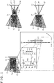
- Examples of the configuration of typical image-capturing apparatuses include a pinhole camera as illustrated at the lower right section in FIG. 1 .
- the image-capturing apparatus including the pinhole camera includes a solid-state image-capturing device 11 and a pinhole 21 provided as a hole section through a light-blocking film 12.
- a solid-state image-capturing device 11 and a pinhole 21 provided as a hole section through a light-blocking film 12.
- light rays L1 to L3 emitted from mutually different light sources on a subject plane are individually transmitted through the pinhole 21, and captured as images at pixels I1 to 13 on the solid-state image-capturing device 11.
- an image is formed with only a light ray that is included in the light rays L1 to L3 emitted from the individual light sources, and corresponds to one pixel, and enters the corresponding pixel on the solid-state image-capturing device 11. Accordingly, the image is captured as a dark pictorial image.
- an image-capturing lens 32 is provided at a middle of a light-blocking film 31, the image-capturing lens 32 concentrates the light rays L1 to L3 as illustrated by light rays I11 to 113, and forms individual images on the solid-state image-capturing device 11, and those images are captured by the solid-state image-capturing device 11.
- the set of the individual point light sources constitute at least part of a subject. Accordingly, in image-capturing of the subject, light rays emitted from a plurality of point light sources on the subject plane are concentrated, and an image of the subject formed thereby is captured.
- a role of the image-capturing lens 32 is to guide each light ray exiting one of the point light sources, that is, spread light, onto the solid-state image-capturing device 11. Accordingly, this results in formation of an image corresponding to a final pictorial image on the solid-state image-capturing device 11, and a pictorial image formed with detection signals detected at the individual pixels on the solid-state image-capturing device 11 becomes a captured pictorial image in which the image is formed.
- an image of a subject on a subject plane is captured by using the solid-state image-capturing device 11 and a mask 51 without providing an image-capturing lens and a pinhole.
- the mask 51 including opening sections 51a with a plurality of sizes is provided before the solid-state image-capturing device 11, and the light rays L1 to L3 from the individual light sources are modulated, enter the image-capturing plane of the solid-state image-capturing device 11, and are received by the individual pixels on the solid-state image-capturing device 11.
- the light sources of the light rays L1 to L3 at the upper left section in FIG. 1 may be point light sources PA, PB, and PC, and light rays with light intensities a, b, and c may enter each of positions Pa, Pb, and Pc on the solid-state image-capturing device 11 where the light rays enter after being transmitted through the mask 51.
- the detection sensitivity of each pixel is given a directionality according to the angle of incidence of incident light since the incident light is modulated by the opening sections 51a randomly set through the mask 51. That the detection sensitivity of each pixel is given an angle-of-incidence directionality mentioned here means that the photosensitivity characteristics according to the angles of incidence of incident light are made different depending on areas on the solid-state image-capturing device 11.
- the light sources constituting at least part of a subject plane 71 are point light sources
- detection signal levels DA, DB, and DC of the pixels at the positions Pa, Pb, and Pc on the solid-state image-capturing device 11 are represented by the following Formula (1) to Formula (3), respectively.
- DA ⁇ 1 ⁇ a + ⁇ 1 ⁇ b + ⁇ 1 ⁇ c
- DB ⁇ 2 ⁇ a + ⁇ 2 ⁇ b + ⁇ 2 ⁇ c
- DC ⁇ 3 ⁇ a + ⁇ 3 ⁇ b + ⁇ 3 ⁇ c
- ⁇ 1 is a coefficient for the detection signal level a set according to the angle of incidence of a light ray from the point light source PA on the subject plane 71 to be restored at the position Pa on the solid-state image-capturing device 11.
- ⁇ 1 is a coefficient for the detection signal level b set according to the angle of incidence of a light ray from the point light source PB on the subject plane 71 to be restored at the position Pa on the solid-state image-capturing device 11.
- ⁇ 1 is a coefficient for the detection signal level c set according to the angle of incidence of a light ray from the point light source PC on the subject plane 71 to be restored at the position Pa on the solid-state image-capturing device 11.
- ( ⁇ 1 ⁇ a) in the detection signal level DA indicates the detection signal level of the light ray from the point light source PA at the position Pc.
- ( ⁇ 1 ⁇ b) in the detection signal level DA indicates the detection signal level of the light ray from the point light source PB at the position Pc.
- ( ⁇ 1 ⁇ c) in the detection signal level DA indicates the detection signal level of the light ray from the point light source PC at the position Pc.
- the detection signal level DA is expressed as a composite value of the individual components of the point light sources PA, PB, and PC at the position Pa multiplied by the coefficients ⁇ 1, ⁇ 1, and ⁇ 1, respectively.
- the coefficients ⁇ 1, ⁇ 1, and ⁇ 1 are collectively called a coefficient set.
- a coefficient set ⁇ 2, ⁇ 2, and ⁇ 2 in the detection signal level DB at the point light source PB corresponds to the coefficient set ⁇ 1, ⁇ 1, and ⁇ 1, respectively, in the detection signal level DA at the point light source PA.
- a coefficient set ⁇ 3, ⁇ 3, and ⁇ 3 in the detection signal level DC at the point light source PC corresponds to the coefficient set ⁇ 1, ⁇ 1, and ⁇ 1, respectively, in the detection signal level DA at the point light source PA.
- the detection signal levels of the pixels at the positions Pa, Pb, and Pc are values expressed by the sum of the products of the light intensities a, b, and c of the light rays emitted from the point light sources PA, PB, and PC, respectively, by the coefficients. Because of this, these detection signal levels are mixtures of the light intensities a, b, and c of the light rays emitted from the point light sources PA, PB, and PC, respectively, and accordingly are different from those with which an image of the subjects is formed.
- detection signal levels illustrated at the upper right section in FIG. 1 are not detection signal levels corresponding to a pictorial image in which an image of the subject is formed, and so are not pixel values.
- detection signal levels illustrated at the lower right section in FIG. 1 are each the signal value of each pixel corresponding to a pictorial image in which an image of a subject is formed, that is, the value of each pixel of a restored pictorial image (final pictorial image), and so are pixel values.
- a pictorial image that has been captured by a solid-state image-capturing device, and has not been reconstructed is referred to simply as a captured pictorial image
- a pictorial image that has been reconstructed and restored by performing signal processing on the captured pictorial image is referred to as a final pictorial image (restored pictorial image). Accordingly, from a single captured pictorial image, pictorial images on subject planes 71 at various distances can be reconstructed as final pictorial images by changing the coefficient sets mentioned above in various manners.
- the significance of the influence of diffraction can be changed by the wavelength of incident light, and the unit size which is the minimum unit for adjusting the sizes of the opening sections 51a.
- the mask 51 and the solid-state image-capturing device 11 are divided into a plurality of areas, and a band-pass filter that varies the wavelength band of incident light is provided for each divided area before the mask 51. Then, the sizes of the opening sections 51a are provided on the mask 51 with the unit sizes according to the wavelength bands of light to be transmitted by the band-pass filters of the individual areas such that the influence of spreading of the incident light resulting from diffraction is reduced.
- a captured pictorial image is captured in each area while the influence of diffraction is reduced appropriately according to the wavelength band of incident light set for each area, a final pictorial image of each area is reconstructed by performing signal processing, and the final pictorial images are synthesized.
- the lensless image-capturing apparatus it becomes possible in the lensless image-capturing apparatus to reduce the influence of blurring due to diffraction, and to reconstruct final pictorial images with high spatial resolutions in image-capturing by using incident light in a wide range of incident-light wavelength bands.
- FIG. 3 illustrates a configuration example of an image-capturing device in a typical lensless image-capturing apparatus
- the upper left section is a top view of the mask 51
- the lower left section is a perspective view of the mask 51 and the solid-state image-capturing device 11 as seen laterally and obliquely from above.
- the right section in FIG. 3 illustrates a configuration example of an image-capturing device in a typical lensless image-capturing apparatus
- the upper left section is a top view of the mask 51
- the lower left section is a perspective view of the mask 51 and the solid-state image-capturing device 11 as seen laterally and obliquely from above.
- the upper right section is a top view of a mask 102
- the lower right section is a perspective view of the mask 102 and a solid-state image-capturing device 101 in a state that a band-pass filter 103 is provided before the mask 102 as seen laterally and obliquely from above.
- the unit size of the opening sections 51a of the mask 51 is set uniformly for all the areas, and at the solid-state image-capturing device 11, a single pictorial image is captured as a whole by using light that has been transmitted through the mask 51.
- each of the solid-state image-capturing device 101, the mask 102, and the band-pass filter 103 is divided into four areas in total by dividing each of them into two areas in both the horizontal direction and the vertical direction, and four captured pictorial images for identical subjects are captured by using incident light in mutually different wavelength bands that enter the individual areas.
- the mask 102 is divided into four areas in total including areas 102A to 102D, and in the areas 102A to 102D, opening sections 102a to 102d with different unit sizes are provided, respectively.
- the unit sizes of the opening sections 102a to 102d are set randomly according to the wavelength bands of light that are transmitted through individual areas 103A to 103D of the band-pass filter 103 provided before the mask 102.
- the unit size of the opening sections 102a of the area 102A is set to such a unit size that the influence of diffraction is minimized when light in a wavelength band to be transmitted through the area 103A of the band-pass filter 103 is transmitted.
- the unit size of the opening sections 102b of the area 102B is set to such a unit size that the influence of diffraction is minimized when light in a wavelength band to be transmitted through the area 103B of the band-pass filter 103 is transmitted.
- the unit size of the opening sections 102c of the area 102C is set to such a unit size that the influence of diffraction is minimized when light in a wavelength band to be transmitted through the area 103C of the band-pass filter 103 is transmitted.
- the unit size of the opening sections 102d of the area 102D is set to such a unit size that the influence of diffraction is minimized when light in a wavelength band to be transmitted through the area 103D of the band-pass filter 103 is transmitted.
- the solid-state image-capturing device 101 is also divided into four areas, areas 101A to 101D, such that those areas correspond to the areas 102A to 102D, and the area 101A of the solid-state image-capturing device 101 captures a captured pictorial image A formed with light in the wavelength band transmitted through the area 103A of the band-pass filter 103.
- the area 101B of the solid-state image-capturing device 101 captures a captured pictorial image B formed with light in the wavelength band transmitted through the area 103B of the band-pass filter 103.
- the area 101C of the solid-state image-capturing device 101 captures a captured pictorial image C formed with light in the wavelength band transmitted through the area 103C of the band-pass filter 103.
- the area 101D of the solid-state image-capturing device 101 captures a captured pictorial image D formed with light with a wavelength transmitted through the area 103D of the band-pass filter 103.
- lensless image-capturing apparatus lensless image-capturing apparatus
- FIG. 4 a configuration example of the lensless image-capturing apparatus (lensless image-capturing apparatus) of the present disclosure is explained with reference to FIG. 4 .
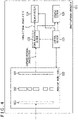
- FIG. 4 illustrates a configuration example of the lateral cross-sectional of a lensless image-capturing apparatus 111 of the present disclosure. More specifically, the lensless image-capturing apparatus 111 in FIG. 4 includes a control section 121, an image-capturing device 122, a signal processing section 123, a display section 124, and a storage section 125.
- the control section 121 includes a processor and the like, and controls overall operations of the lensless image-capturing apparatus 111.
- the image-capturing device 122 has the configuration explained with reference to the right section in FIG. 3 , captures, as captured pictorial images, pictorial images formed with pixel signals according to the light amount of incident light from a subject indicated by the right arrow in FIG. 4 , and outputs the captured pictorial images to the signal processing section 123.
- the image-capturing device 122 corresponds to the right section in FIG. 3 , and includes the band-pass filter 103, the mask 102, and the solid-state image-capturing device 101 from the left side in the figure.
- the band-pass filter 103 is divided into two areas in both the horizontal direction and the vertical direction, that is, divided into four areas in total, the areas 103A to 103D, and the different areas transmit light in different wavelength bands of incident light.
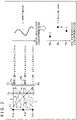
- the area 103A of the band-pass filter 103 transmits incident light in a wavelength band ZA near predetermined wavelengths ⁇ 1 to ⁇ 1+ ⁇ of the incident light
- the area 103B transmits incident light in a wavelength band ZB near predetermined wavelengths ⁇ 1+ ⁇ to ⁇ 1+2 ⁇ of the incident light
- the area 103C transmits incident light in a wavelength band ZC near predetermined wavelengths ⁇ 1+2 ⁇ to ⁇ 1+3 ⁇ of the incident light
- the area 103D transmits incident light in a wavelength band ZD near predetermined wavelengths ⁇ 1+3 ⁇ to ⁇ 1+4 ⁇ of the incident light.
- ⁇ 1 is a predetermined wavelength of the incident light
- ⁇ is a predetermined constant
- the areas 103A to 103D of the band-pass filter 103 transmit the incident light in the mutually different wavelength bands ZA to ZD of the incident light.
- the wavelength bands ZA to ZD are wavelength bands having nearly identical widths in FIG. 5 , they need not have identical widths, and may have different widths.
- the mask 102 is divided into the areas 102A to 102D such that those areas correspond to the areas 103A to 103D of the band-pass filter 103.
- the unit size ⁇ (see the lower left section in FIG. 1 ) for adjusting the intervals between light-blocking sections and opening sections in each mask is adjusted such that the influence of diffraction is minimized corresponding to the wavelength of light to be transmitted.
- the magnitude of diffraction that occurs in a case that incident light is transmitted through the mask 102 varies depending on the wavelength of the transmitted light, and the unit size ⁇ for adjusting the sizes of the opening sections.
- the unit size ⁇ is varied in increments of a predetermined width ⁇ from ⁇ 1 to ⁇ 1+7 ⁇ from the left side in the figure, captured pictorial images of incident light passing through one opening section captured by the solid-state image-capturing device 101 vary as illustrated by captured pictorial images F1 to F8.
- incident-light pictorial images that are formed with the incident light do not become spot-like pictorial images on the image-capturing plane of the solid-state image-capturing device 101, and become pictorial images that present scattered and spreading light, and furthermore the magnitude of the spreading varies depending on the degree of the influence of diffraction.
- the unit size ⁇ decreases as illustrated by the captured pictorial images F3, F2, and F1 or as the unit size ⁇ increases as illustrated by the captured pictorial images F5 to F8, the spots near the centers spread, and the influence of diffraction gradually increases.
- the captured pictorial image F15 presents the brightest spot with the smallest diameter, and it can be considered that the influence of diffraction is minimized.
- the unit size ⁇ decreases as illustrated by the captured pictorial images F14, F13, F12, and F11 or as the unit size ⁇ increases as illustrated by the captured pictorial images F16 to F18, the spots near the centers spread, and the influence of diffraction gradually increases.
- the unit size ⁇ decreases as illustrated by the captured pictorial images F24, F23, F22, and F21 or as the unit size ⁇ increases as illustrated by the captured pictorial images F26 to F28, the spots near the centers spread, and the influence of diffraction gradually increases.
- the unit size ⁇ decreases as illustrated by the captured pictorial images F35, F34, F33, F32, and F31 or as the unit size ⁇ increases as illustrated by the captured pictorial images F26 to F28, the spots near the centers spread, and the influence of diffraction gradually increases.
- incident light can be modulated, and caused to enter the solid-state image-capturing device 101 in a state that the influence of diffraction occurring to light in the wavelength band is minimized, by setting the unit sizes ⁇ of the opening sections 102a to 102d in the areas 102A to 102D of the corresponding mask 102 to ⁇ 1+3 ⁇ , ⁇ 1+4 ⁇ , ⁇ 1+4 ⁇ , and ⁇ 1+5 ⁇ , respectively.
- the areas 101A to 101D of the solid-state image-capturing device 101 it becomes possible for the areas 101A to 101D of the solid-state image-capturing device 101 to capture four captured pictorial images of the individual wavelength bands each with minimized influence of blurring due to diffraction.
- the solid-state image-capturing device 101 is at least partially constituted by a CMOS image sensor or the like, captures a captured pictorial image formed with a pixel signal according to the light amount of incident light in each pixel unit, and outputs the captured image to the signal processing section 123.
- the solid-state image-capturing device 101 is divided into the areas 101A to 101D such that those areas correspond to the areas 103A to 103D of the band-pass filter 103, respectively, and the areas 102A to 102D of the mask 102, respectively, captures the four captured pictorial images A to D in total of identical spatial ranges formed with incident light in different wavelength bands for the different areas, and outputs the captured images A to D to the signal processing section 123.
- the signal processing section 123 solves simultaneous equations as explained, for example, by using FIG. 2 and Formula (1) to Formula (3) for pictorial-image signals of the captured pictorial images A to D supplied from the image-capturing device 122, to thereby reconstruct and synthesize the final pictorial images A to D for the areas 101A to 101D, and outputs the final pictorial images A to D as a single final pictorial image to the display section 124 and causes the single final pictorial image to be displayed on the display section 124, or causes the one final pictorial image to be stored in the storage section 125.
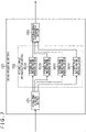
- the signal processing section 123 includes a signal area dividing section 131, a pictorial-image reconstructing section 132, and a pictorial-image synthesizing section 133.
- the signal area dividing section 131 divides a pictorial image supplied from the image-capturing device 122 into the captured pictorial images A to D each formed with a pixel signal of a corresponding area of the areas 101A to 101D, and outputs the captured pictorial images A to D to pictorial-image reconstruction processing sections 151A to 151D of the pictorial-image reconstructing section 132, respectively.
- the pictorial-image reconstructing section 132 solves simultaneous equations as explained with reference to FIG. 2 and Formula (1) to Formula (3) for each of the four captured pictorial images A to D divided into the areas 101A to 101D, respectively, by the signal area dividing section 131, to thereby reconstruct the captured pictorial images A to D as the final pictorial images A to D, and outputs the reconstructed final pictorial images A to D to the pictorial-image synthesizing section 133.
- the pictorial-image reconstructing section 132 includes the pictorial-image reconstruction processing sections 151A to 151D that reconstruct the final pictorial images A to D from the captured pictorial images A to D of the areas 101A to 101D, respectively, divided by the signal area dividing section 131.
- the pictorial-image reconstruction processing sections 151A to 151D respectively reconstruct the final pictorial images A to D from the captured pictorial images A to D of the areas 101A to 101D, respectively, divided by the signal area dividing section 131, and outputs the final pictorial images A to D to the pictorial-image synthesizing section 133.
- the pictorial-image synthesizing section 133 synthesizes the final pictorial images A to D reconstructed from the captured pictorial images A to D of the areas 101A to 101D of the solid-state image-capturing device 101 supplied from the pictorial-image reconstruction processing sections 151A to 151D of the pictorial-image reconstructing section 132, in such a manner that the final pictorial images A to D are superimposed, to form a single pictorial image.
- the pictorial-image synthesizing section 133 outputs the single pictorial image to the display section 124, and causes the one pictorial image to be displayed on the display section 124.
- the pictorial-image synthesizing section 133 outputs the one pictorial image to the storage section 125, and causes the one pictorial image to be stored in the storage section 125.
- each of the areas 103A to 103D of the band-pass filter 103 transmits light in the corresponding one of the wavelength bands ZA to ZD of incident light that are explained with reference to FIG. 2 .
- each of the areas 102A to 102D of the mask 102 modulates the incident light by the corresponding one of the opening sections 102a to 102d according to the unit size ⁇ , and causes the incident light to enter the image-capturing plane of the solid-state image-capturing device 101.
- each of the areas 101A to 101D of the solid-state image-capturing device 101 captures a corresponding one of the captured pictorial images A to D formed with the light modulated by being transmitted through the areas 102A to 102D of the mask 102, and the captured pictorial images A to D are output to the signal processing section 123 as a single captured pictorial image.
- Step S14 the signal area dividing section 131 of the signal processing section 123 divides the captured pictorial image supplied from the solid-state image-capturing device 101 of the image-capturing device 122 into the captured pictorial images A to D of the areas 101A to 101D, respectively, and outputs the captured pictorial images A to D to the pictorial-image reconstruction processing sections 151A to 151D of the pictorial-image reconstructing section 132, respectively.
- Step S15 the pictorial-image reconstruction processing sections 151A to 151D reconstruct the captured pictorial images A to D captured by the areas 101A to 101D of the solid-state image-capturing device 101, respectively, by the process explained with reference to FIG. 2 and Formula (1) to Formula (3), generates the final pictorial images A to D and outputs the final pictorial images A to D to the pictorial-image synthesizing section 133.
- Step S16 the pictorial-image synthesizing section 133 synthesizes the final pictorial images A to D obtained from the four captured pictorial images A to D, respectively, captured by the areas 101A to 101D in such a manner that the final pictorial images A to D are superimposed, and outputs the final pictorial images A to D as a single final pictorial image.
- light is modulated by the opening sections and the light-blocking sections that have sizes according to the unit sizes ⁇ of the individual areas 102A to 102D of the mask 102 according to the wavelength bands of incident light.
- the temperature of a target is determined from the peak wavelength of integrated light in a wide range of long wavelength bands. More specifically, the range of wavelength bands to be sensed is typically considered to be around 8 to 14 ⁇ m. In this case, the longest wavelength of the sensing target is approximately twice as long as the shortest wavelength of the sensing target.
- the wavelength ⁇ 1 mentioned above in FIG. 5 is set to 8 ⁇ m, ⁇ is set to 1.5 ⁇ m, and the wavelength bands ZA to ZD are set to wavelength bands near 8 to 9.5 ⁇ m, 9.5 to 11 ⁇ m, 11 to 12.5 ⁇ m, and 12.5 to 14 ⁇ m.
- the range of near infrared light to far infrared light can be set as appropriate wavelength bands.
- the unit size ⁇ of each of the areas 102A to 102D of the mask 102 is set such that the influence of diffraction is reduced in each wavelength band. Thereby, it becomes possible to realize image-capturing of temperature information less influenced by blurring due to diffraction.
- wavelength bands ZA to ZD mentioned above may be set to other wavelength bands, and, for example, may be set to RGB (red, green, and blue visible light) and IR (infrared light).
- each of the band-pass filter 103, the mask 102, and the solid-state image-capturing device 101 is divided into four areas according to wavelength bands, the captured pictorial images A to D are captured in the individual areas, and the final pictorial images A to D are reconstructed by performing signal processing by using the captured pictorial images A to D to synthesize the final pictorial images A and D into a single final pictorial image.
- the number of the divided areas may be any number other than four, and the band-pass filter 103, the mask 102, and the solid-state image-capturing device 101 may be divided into a larger number of areas only to the extent that such division does not cause significant deterioration of resolution.
- the sizes of the individual areas are desirably approximately identical to each other; however, they do not have to strictly be identical, and they are only required to have such sizes that a spatial range that is required in the final pictorial images is covered by the captured pictorial images as a whole.
- the pictorial-image synthesizing section 133 may synthesize the plurality of pictorial images after performing parallax correction according to the positions of the pictorial images captured in the plurality of areas in the one solid-state image-capturing device 101. Thereby, the spatial resolution can be improved.
- the pictorial-image synthesizing section 133 synthesizes a plurality of reconstructed final pictorial images into a single pictorial image in such a manner that the plurality of reconstructed final pictorial images is superimposed
- the plurality of reconstructed final pictorial images may be regarded as being synthesized as long as a single pictorial image can eventually be generated by using the plurality of final pictorial images.
- the pictorial-image synthesizing section 133 may synthesize the plurality of final pictorial images by selecting a single final pictorial image from the plurality of final pictorial images, for example.
- the single final pictorial image to be selected here may be a pictorial image which is least influenced by diffraction, for example.
- the pictorial-image synthesizing section 133 may select a plurality of final pictorial images from the plurality of final pictorial images, and synthesize the plurality of final pictorial images in such a manner that the selected final pictorial images are superimposed, for example.
- the plurality of final pictorial images to be selected here may be a plurality of final pictorial images which is relatively less influenced by diffraction, for example.
- each of the band-pass filter 103, the mask 102, and the solid-state image-capturing device 101 is divided into a plurality of corresponding areas, the wavelength band of incident light to be transmitted by the band-pass filter 103 is set for each divided area, and incident light is modulated by the mask 102 including opening sections each having the unit size according to the wavelength band for a corresponding area.
- a captured pictorial image is captured in each area in a state that the influence of diffraction is reduced, a final pictorial image is reconstructed from the captured pictorial image captured in each area, and the final pictorial images of the individual areas are synthesized.
- a single final pictorial image with a high spatial resolution is captured by reducing the influence of blurring due to diffraction.
- the degree of the influence of diffraction can also be adjusted by the distance between the mask 102 and the solid-state image-capturing device 101 according to the wavelength band of incident light.
- the opening sections of the mask 102 may be formed to have identical unit sizes ⁇ in all the areas, and the distance between the mask 102 and the solid-state image-capturing device 101 may be varied for each area according to the wavelength band of incident light to reduce the influence of diffraction.
- FIG. 9 illustrates a configuration example of the image-capturing device 122 of the lensless image-capturing apparatus 111 in which the opening sections of the mask 102 are formed to have identical unit sizes ⁇ in all the areas, and the distance between the mask 102 and the solid-state image-capturing device 101 is varied for each area according to the wavelength band of incident light to reduce the influence of diffraction.
- FIG. 9 configurations in FIG. 9 that have functions identical to those in FIG. 3 are given identical reference signs, and explanations thereof are omitted as appropriate. That is, a difference of FIG. 9 from FIG. 3 is that instead of the area 102A to the area 102D of the mask 102 and the areas 103A to 103D of the band-pass filter 103, areas 102A' to 102D' and areas 103A' to 103D' are set.
- FIG. 9 descriptions of mask patterns for the areas 102A' and 102B' are omitted, the omission is only for convenience of explanation, and mask patterns with identical unit sizes are actually provided to the areas 102A' to 102D'.
- the distances between the areas 101A to 101D of the solid-state image-capturing device 101 and the areas 102A' to 102D' of the mask 102, respectively, are different from each other.
- the distance between the area 101A of the solid-state image-capturing device 101 and the area 102A' of the mask 102 is a distance GapA
- the distance between the area 101B of the solid-state image-capturing device 101 and the area 102B' of the mask 102 is a distance GapB
- the distance between the area 101C of the solid-state image-capturing device 101 and the area 102C' of the mask 102 is a distance GapC
- the distance between the area 101D of the solid-state image-capturing device 101 and the area 102D' of the mask 102 is a distance GapD
- GapA to GapD are mutually different distances.
- the wavelength of incident light is the wavelength ⁇ 1
- the distance between the mask 102 and the solid-state image-capturing device 101 is varied from G1 to G1+11 ⁇
- captured pictorial images of incident light passing through one opening section captured by the solid-state image-capturing device 101 vary as illustrated by captured pictorial images F101 to F108.
- incident-light pictorial images that are formed with the incident light do not become spot-like pictorial images on the image-capturing plane of the solid-state image-capturing device 101, but become pictorial images that present scattered and spreading light, and furthermore the magnitude of the spreading varies depending on the degree of the influence of diffraction.
- the pictorial image F106 presents the brightest spot with the smallest diameter, and it can be considered that the influence of diffraction is minimized.
- the distance between the mask 102 and the solid-state image-capturing device 101 decreases as illustrated by the pictorial images F105 to F101 or as the distance between the mask 102 and the solid-state image-capturing device 101 increases as illustrated by the pictorial image F107, the spots near the centers spread, and the influence of diffraction gradually increases.
- the wavelength of incident light is the wavelength ⁇ 1+ ⁇
- the distance between the mask 102 and the solid-state image-capturing device 101 is varied from G1 to G1+11 ⁇
- captured pictorial images of incident light passing through one opening section captured by the solid-state image-capturing device 101 vary as illustrated by the captured pictorial images F111 to F118.
- the captured pictorial image F115 presents the brightest spot with the smallest diameter, and it can be considered that the influence of diffraction is minimized.
- the distance between the mask 102 and the solid-state image-capturing device 101 decreases as illustrated by the captured pictorial images F114 to F111 or as the distance between the mask 102 and the solid-state image-capturing device 101 increases as illustrated by the captured pictorial images F116 and F117, the spots near the centers spread, and the influence of diffraction gradually increases.
- the wavelength of incident light is the wavelength ⁇ 1+2 ⁇
- the distance between the mask 102 and the solid-state image-capturing device 101 is varied from G1 to G1+11 ⁇
- captured pictorial images of incident light passing through one opening section captured by the solid-state image-capturing device 101 vary as illustrated by captured pictorial images F121 to F128.
- the captured pictorial image F124 presents the brightest spot with the smallest diameter, and it can be considered that the influence of diffraction is minimized.
- the distance between the mask 102 and the solid-state image-capturing device 101 decreases as illustrated by the captured pictorial images F123 to F121 or as the distance between the mask 102 and the solid-state image-capturing device 101 increases as illustrated by the captured pictorial image F125 to F127, the spots near the centers spread, and the influence of diffraction gradually increases.
- the wavelength of incident light is the wavelength ⁇ 1+3 ⁇
- the distance between the mask 102 and the solid-state image-capturing device 101 is varied from G1 to G1+11 ⁇
- captured pictorial images of incident light passing through one opening section captured by the solid-state image-capturing device 101 vary as illustrated by the captured pictorial images F131 to F138.
- the captured pictorial image F133 presents the brightest spot with the smallest diameter, and it can be considered that the influence of diffraction is minimized.
- the distance between the mask 102 and the solid-state image-capturing device 101 decreases as illustrated by the captured pictorial images F132 and F131 or as the distance between the mask 102 and the solid-state image-capturing device 101 increases as illustrated by the captured pictorial images F134 to F137, the spots near the centers spread, and the influence of diffraction gradually increases.
- incident light can be modulated, and caused to enter the solid-state image-capturing device 101 in a state that diffraction occurring to light in the individual wavelength bands is minimized by setting the distances GapA to GapD of the areas 102A' to 102D' of the corresponding mask 102 and the areas 101A to 101D of the corresponding solid-state image-capturing device 101 to G1+9 ⁇ , G1+7 ⁇ , G1+5 ⁇ , and G1+3 ⁇ , respectively.
- the solid-state image-capturing device 101 it becomes possible for the solid-state image-capturing device 101 to capture four captured pictorial images of the individual wavelength bands each with minimized influence of blurring due to diffraction.
- both unit sizes of the mask 102, and distances between the mask 102 and the solid-state image-capturing device 101 may be adjusted for the individual areas that transmit identical wavelength bands.
- each of the band-pass filter 103, the mask 102, and the solid-state image-capturing device 101 is divided into areas according to wavelength bands of light to be transmitted by the band-pass filter 103, the light is modulated by the mask 102 in the individual areas such that the influence of diffraction is minimized for the individual wavelength bands in the individual areas, and captured by the solid-state image-capturing device 101, a final pictorial image of each area is reconstructed from a captured pictorial image captured in the area, and the final pictorial images are synthesized into a single final pictorial image.
- FIG. 11 illustrates a configuration example of the image-capturing device 122 of the lensless image-capturing apparatus 111 in which light-blocking walls are provided at the boundaries between divided areas. Note that configurations in FIG. 11 that have functions identical to those in FIG. 3 are given identical reference signs, and explanations thereof are omitted.
- FIG. 11 a difference of FIG. 11 from the image-capturing device of the lensless image-capturing apparatus in FIG. 3 is that light-blocking walls 201-1 and 201-2 are provided at the boundaries between the areas 103A to 130D of the band-pass filter 103, between the areas 102A to 102D of the mask 102, and between the areas 101A to 101D of the solid-state image-capturing device 101.
- the light-blocking walls 201-1 and 201-2 being provided at the boundaries between the areas 103A to 130D of the band-pass filter 103, between the areas 102A to 102D of the mask 102, and between the areas 101A to 101D of the solid-state image-capturing device 101, it becomes possible to prevent color mixing due to light in adjacent wavelength bands near the boundaries between the individual areas, and it becomes possible to surely reduce the influence of diffraction in the individual areas.
- a system means a set of a plurality of constituent elements (apparatuses, modules (parts), etc.), and it does not matter whether or not all the constituent elements are contained in a single housing. Accordingly, both a plurality of apparatuses that is housed in separate housings and connected via a network, and one apparatus in which a plurality of modules is housed in one housing are systems.
- each step explained in the flowchart mentioned above can be executed not only by one apparatus, but also by a plurality of apparatuses by being shared among the plurality of apparatuses.
- one step includes a plurality of processes
- the plurality of processes included in the one step can be executed not only by one apparatus, but also by a plurality of apparatuses by being shared among the plurality of apparatuses.
- Solid-state image-capturing device 101A to 101D, 101A' to 101D' Area, 102 Mask, 102A to 102D, 102A' to 102D' Area, 103 Band-pass filter, 103A to 103D, 103A' to 103D' Area, 111 Lensless image-capturing apparatus, 121 Control section, 122 Image-capturing device, 123 Signal processing section, 124 Display section, 125 Storage section, 131 Signal area dividing section, 132 Pictorial-image reconstructing section, 133 Pictorial-image synthesizing section, 151A to 151D Pictorial-image reconstruction processing section
Landscapes
- Physics & Mathematics (AREA)
- Engineering & Computer Science (AREA)
- General Physics & Mathematics (AREA)
- Optics & Photonics (AREA)
- Computing Systems (AREA)
- Theoretical Computer Science (AREA)
- Multimedia (AREA)
- Signal Processing (AREA)
- Studio Devices (AREA)
- Optical Filters (AREA)
- Transforming Light Signals Into Electric Signals (AREA)
- Color Television Image Signal Generators (AREA)
Claims (14)
- Dispositif de capture d'images (122) comprenant :un filtre passe-bande (103) qui est divisé en une pluralité de zones, dont chacune transmet de la lumière incidente dans une bande de longueurs d'onde différente ;un masque (102) qui est divisé de façon correspondante à la pluralité de zones, et module la lumière incidente dans les différentes bandes de longueurs d'onde qui sont chacune transmises à travers une zone correspondante de la pluralité de zones du filtre passe-bande (103) ;un dispositif de capture d'images à semi-conducteurs (101) qui a un plan de capture d'images qui est divisé de façon correspondante à la pluralité de zones, et capture, sous la forme d'un signal de pixels bidimensionnels, la lumière incidente modulée par le masque (102) dans chacune de la pluralité de zones, une distance entre le masque (102) et le plan de capture d'images du dispositif de capture d'images à semi-conducteurs (101) différant pour chacune de la pluralité de zones.
- Dispositif de capture d'images (122) selon la revendication 1, dans lequel
le masque (102) a un motif de masque ayant une taille unitaire qui est différente pour chacune de la pluralité de zones. - Dispositif de capture d'images (122) selon la revendication 2, dans lequel
le motif de masque pour chacune de la pluralité de zones est un motif de masque ayant une taille unitaire différente qui est basée sur la bande de longueurs d'onde de la lumière incidente qui est transmise à travers le filtre passe-bande. - Dispositif de capture d'images (122) selon la revendication 2, dans lequel
le motif de masque pour chacune de la pluralité de zones est un motif de masque ayant une taille unitaire telle que, lorsque la lumière incidente dans la bande de longueurs d'onde qui est transmise à travers le filtre passe-bande (103) est capturée par le dispositif de capture d'images à semi-conducteurs (101), l'étalement de la lumière incidente dû à la diffraction est approximativement minimisé. - Dispositif de capture d'images (122) selon la revendication 1, dans lequel
la distance entre le masque (102) et le plan de capture d'images du dispositif de capture d'images à semi-conducteurs (101) est une distance qui diffère sur une base de la bande de longueurs d'onde de la lumière incidente qui est transmise à travers chacune de la pluralité de zones du filtre passe-bande (103). - Dispositif de capture d'images (122) selon la revendication 5, dans lequel
la distance entre le masque (102) et le plan de capture d'images du dispositif de capture d'images à semi-conducteurs (101) pour chacune de la pluralité de zones est une distance telle que, lorsque la lumière incidente dans la bande de longueurs d'onde qui est transmise à travers le filtre passe-bande (103) est capturée par le dispositif de capture d'images à semi-conducteurs (101), l'étalement de la lumière incidente dû à la diffraction est approximativement minimisé. - Dispositif de capture d'images (122) selon la revendication 1, dans lequel
le masque (102) a un motif de masque ayant des tailles unitaires identiques pour toutes les zones de la pluralité de zones. - Dispositif de capture d'images (122) selon la revendication 1, comprenant en outre ;
une paroi bloquant la lumière (201-1, 201-2) qui bloque la lumière incidente provenant de zones adjacentes au niveau d'une limite entre la pluralité de zones du filtre passe-bande (103), le masque (102), et le dispositif de capture d'images à semi-conducteurs (101). - Appareil de capture d'images (111) comprenant :
un dispositif d'imagerie (122) comprenant :un filtre passe-bande (103) qui est divisé en une pluralité de zones, dont chacune transmet de la lumière incidente dans une bande de longueurs d'onde différente,un masque (102) qui est divisé de façon correspondante à la pluralité de zones, et module la lumière incidente dans les différentes bandes de longueurs d'onde qui sont chacune transmises à travers une zone correspondante de la pluralité de zones du filtre passe-bande (103), etun dispositif de capture d'images à semi-conducteurs (101) qui a un plan de capture d'images qui est divisé de façon correspondante à la pluralité de zones, et capture, sous la forme d'un signal de pixels bidimensionnels, la lumière incidente modulée par le masque (102) dans chacune de la pluralité de zones, une distance entre le masque (102) et le plan de capture d'images du dispositif de capture d'images à semi-conducteurs (101) différant pour chacune de la pluralité de zones ; etune section de traitement du signal (123) qui reconstruit, sous la forme d'une image picturale finale par traitement du signal, les signaux de pixels bidimensionnels capturés par le dispositif de capture d'images à semi-conducteurs (101). - Appareil de capture d'images (111) selon la revendication 9, dans lequel
la section de traitement du signal (123) comporte :une section de division (131) qui divise un signal de pixels bidimensionnels capturé par le dispositif de capture d'images à semi-conducteurs (101) en association avec la pluralité de zones ;une pluralité de sections de reconstruction d'images picturales (132) qui reconstruit, sous la forme d'une image picturale finale par traitement du signal, chacun de signaux de pixels obtenus par division du signal de pixels bidimensionnels ; etune section de synthèse (133) qui synthétise les images picturales finales reconstruites par la pluralité de sections de reconstruction d'images picturales (132). - Appareil de capture d'images (111) selon la revendication 10, dans lequel
la section de synthèse (133) synthétise les images picturales finales reconstruites par la pluralité de sections de reconstruction d'images picturales (132) en superposant les images picturales finales. - Appareil de capture d'images (111) selon la revendication 10, dans lequel,
en sélectionnant une image picturale finale donnée parmi les images picturales finales reconstruites par la pluralité de sections de reconstruction d'images picturales (132), la section de synthèse (133) synthétise l'image picturale finale donnée. - Appareil de capture d'images (111) selon la revendication 10, dans lequel
la section de synthèse (133) sélectionne au moins deux images picturales finales parmi les images picturales finales reconstruites par la pluralité de sections de reconstruction d'images picturales (132), et synthétise les au moins deux images picturales finales sélectionnées de telle sorte que les au moins deux images picturales finales sélectionnées sont superposées. - Procédé de capture d'images d'un appareil de capture d'images (111) comportantun filtre passe-bande (103) qui est divisé en une pluralité de zones, dont chacune transmet de la lumière incidente dans une bande de longueurs d'onde différente,un masque (102) qui est divisé de façon correspondante à la pluralité de zones, et module la lumière incidente dans les différentes bandes de longueurs d'onde qui sont chacune transmises à travers une zone correspondante de la pluralité de zones du filtre passe-bande (103), etun dispositif de capture d'images à semi-conducteurs (101) qui a un plan de capture d'images qui est divisé de façon correspondante à la pluralité de zones, et capture, sous la forme d'un signal de pixels bidimensionnels, la lumière incidente modulée par le masque (102) dans chacune de la pluralité de zones, une distance entre le masque (102) et le plan de capture d'images du dispositif de capture d'images à semi-conducteurs (101) différant pour chacune de la pluralité de zones, le procédé de capture d'images comprenant :
un traitement du signal consistant à reconstruire, sous la forme d'une image picturale finale par traitement du signal, les signaux de pixels bidimensionnels capturés par le dispositif de capture d'images à semi-conducteurs (101) .
Applications Claiming Priority (2)
| Application Number | Priority Date | Filing Date | Title |
|---|---|---|---|
| JP2017246393 | 2017-12-22 | ||
| PCT/JP2018/045019 WO2019124106A1 (fr) | 2017-12-22 | 2018-12-07 | Dispositif d'imagerie, procédé d'imagerie, et élément d'imagerie |
Publications (3)
| Publication Number | Publication Date |
|---|---|
| EP3731521A1 EP3731521A1 (fr) | 2020-10-28 |
| EP3731521A4 EP3731521A4 (fr) | 2020-12-30 |
| EP3731521B1 true EP3731521B1 (fr) | 2022-04-27 |
Family
ID=66992576
Family Applications (1)
| Application Number | Title | Priority Date | Filing Date |
|---|---|---|---|
| EP18892750.3A Not-in-force EP3731521B1 (fr) | 2017-12-22 | 2018-12-07 | Dispositif d'imagerie, procédé d'imagerie, et élément d'imagerie |
Country Status (5)
| Country | Link |
|---|---|
| US (1) | US11283993B2 (fr) |
| EP (1) | EP3731521B1 (fr) |
| JP (1) | JP7283394B2 (fr) |
| CN (1) | CN111448796B (fr) |
| WO (1) | WO2019124106A1 (fr) |
Cited By (1)
| Publication number | Priority date | Publication date | Assignee | Title |
|---|---|---|---|---|
| WO2023237329A1 (fr) * | 2022-06-10 | 2023-12-14 | Ams International Ag | Capteur d'images multispectrales, système de caméra et procédé de fabrication d'un capteur d'image multispectrale |
Families Citing this family (11)
| Publication number | Priority date | Publication date | Assignee | Title |
|---|---|---|---|---|
| FR3077641B1 (fr) * | 2018-02-07 | 2020-02-21 | TiHive | Systeme d'imagerie terahertz a reflexion |
| GB2578769B (en) | 2018-11-07 | 2022-07-20 | Advanced Risc Mach Ltd | Data processing systems |
| GB2583061B (en) * | 2019-02-12 | 2023-03-15 | Advanced Risc Mach Ltd | Data processing systems |
| JP7329532B2 (ja) | 2019-10-18 | 2023-08-18 | グーグル エルエルシー | 大視野画像化のための回折光学素子 |
| CN111128046B (zh) * | 2020-01-16 | 2021-04-27 | 浙江大学 | 一种led显示屏幕的无透镜成像装置及方法 |
| JP7782461B2 (ja) | 2020-12-08 | 2025-12-09 | ソニーグループ株式会社 | 画像処理装置、および画像処理方法、並びにプログラム |
| WO2022130689A1 (fr) * | 2020-12-18 | 2022-06-23 | 株式会社フジクラ | Élément de diffraction optique, système de calcul optique et procédé de fabrication d'élément de diffraction optique |
| JPWO2023145444A1 (fr) | 2022-01-27 | 2023-08-03 | ||
| KR20240173462A (ko) * | 2023-06-05 | 2024-12-12 | 현대모비스 주식회사 | 차량용 디스플레이 장치의 화질 개선 방법 및 시스템 |
| WO2025047424A1 (fr) * | 2023-08-30 | 2025-03-06 | ソニーセミコンダクタソリューションズ株式会社 | Dispositif d'imagerie |
| US12401869B1 (en) * | 2024-07-11 | 2025-08-26 | Erika Blumenfeld | System and method for imaging an astronomical object from space |
Family Cites Families (11)
| Publication number | Priority date | Publication date | Assignee | Title |
|---|---|---|---|---|
| EP2704416B1 (fr) * | 2011-04-25 | 2019-11-27 | Hamamatsu Photonics K.K. | Dispositif d'imagerie |
| US8744200B1 (en) * | 2012-05-04 | 2014-06-03 | Hrl Laboratories, Llc | Hybrid compressive/Nyquist sampling for enhanced sensing |
| US9389105B2 (en) * | 2012-06-21 | 2016-07-12 | The University Of North Carolina At Charlotte | Distributed sensor grid, surface, and skin systems and methods |
| US9081731B2 (en) * | 2013-01-31 | 2015-07-14 | Inview Technology Corporation | Efficient transforms and efficient row generation for Kronecker products of Hadamard matrices |
| WO2014137922A1 (fr) | 2013-03-05 | 2014-09-12 | Rambus Inc. | Réseaux de phase ayant une symétrie impaire pour détection optique sans lentille haute résolution |
| US9110240B2 (en) * | 2013-03-05 | 2015-08-18 | Rambus Inc. | Phase gratings with odd symmetry for high-resolution lensed and lensless optical sensing |
| US9300865B2 (en) * | 2014-01-24 | 2016-03-29 | Goodrich Corporation | Random imaging |
| US9513411B2 (en) * | 2014-07-31 | 2016-12-06 | Visera Technologies Company Limited | Double-lens structures and fabrication methods thereof |
| US9761730B2 (en) * | 2014-10-29 | 2017-09-12 | Semiconductor Energy Laboratory Co., Ltd. | Imaging device and electronic device |
| WO2016123529A1 (fr) | 2015-01-29 | 2016-08-04 | William Marsh Rice University | Système d'imagerie sans lentille utilisant un capteur d'image comprenant une ou plusieurs couches d'atténuation |
| WO2017038542A1 (fr) * | 2015-09-03 | 2017-03-09 | ソニーセミコンダクタソリューションズ株式会社 | Élément de capture d'image à semi-conducteurs et dispositif électronique |
-
2018
- 2018-12-07 EP EP18892750.3A patent/EP3731521B1/fr not_active Not-in-force
- 2018-12-07 US US16/954,015 patent/US11283993B2/en active Active
- 2018-12-07 WO PCT/JP2018/045019 patent/WO2019124106A1/fr not_active Ceased
- 2018-12-07 CN CN201880079342.3A patent/CN111448796B/zh not_active Expired - Fee Related
- 2018-12-07 JP JP2019560961A patent/JP7283394B2/ja active Active
Cited By (1)
| Publication number | Priority date | Publication date | Assignee | Title |
|---|---|---|---|---|
| WO2023237329A1 (fr) * | 2022-06-10 | 2023-12-14 | Ams International Ag | Capteur d'images multispectrales, système de caméra et procédé de fabrication d'un capteur d'image multispectrale |
Also Published As
| Publication number | Publication date |
|---|---|
| US20210084219A1 (en) | 2021-03-18 |
| US11283993B2 (en) | 2022-03-22 |
| EP3731521A1 (fr) | 2020-10-28 |
| CN111448796B (zh) | 2022-04-15 |
| EP3731521A4 (fr) | 2020-12-30 |
| WO2019124106A1 (fr) | 2019-06-27 |
| JP7283394B2 (ja) | 2023-05-30 |
| CN111448796A (zh) | 2020-07-24 |
| JPWO2019124106A1 (ja) | 2021-01-14 |
Similar Documents
| Publication | Publication Date | Title |
|---|---|---|
| EP3731521B1 (fr) | Dispositif d'imagerie, procédé d'imagerie, et élément d'imagerie | |
| JP7528998B2 (ja) | 固体撮像素子、および電子機器 | |
| US9906706B2 (en) | Image sensor and imaging device | |
| CN108700472B (zh) | 使用相对的滤光器掩模进行相位检测自动聚焦 | |
| US9507123B2 (en) | Imaging apparatus | |
| US8854525B2 (en) | Imaging device, imaging system, and imaging method | |
| IL256975A (en) | Method and system for spectral imaging | |
| US20120105844A1 (en) | Coded Aperture Snapshot Spectral Imager and Method Therefor | |
| US9628776B2 (en) | Three-dimensional imaging device, image processing device, image processing method, and image processing program | |
| EP2630788A1 (fr) | Système et procédé d'imagerie utilisant un appareil photo à ouvertures multiples | |
| WO2016071909A1 (fr) | Procédé et système d'imagerie spectrale | |
| US9179127B2 (en) | Three-dimensional imaging device, imaging element, light transmissive portion, and image processing device | |
| US20180013951A1 (en) | Image processing apparatus, image pickup apparatus, image processing method, program, and storage medium | |
| US10021357B2 (en) | Image capturing apparatus and method for generating image data | |
| US9544570B2 (en) | Three-dimensional image pickup apparatus, light-transparent unit, image processing apparatus, and program | |
| US10012953B2 (en) | Method of reconstructing a holographic image and apparatus therefor | |
| US12538042B2 (en) | Imaging device and method for operating imaging device | |
| Rueda et al. | Experimental demonstration of a colored coded aperture-based compressive spectral imaging system | |
| KR102188749B1 (ko) | 초분광 카메라 및 이를 이용한 분광 이미지 추출 방법 |
Legal Events
| Date | Code | Title | Description |
|---|---|---|---|
| STAA | Information on the status of an ep patent application or granted ep patent |
Free format text: STATUS: THE INTERNATIONAL PUBLICATION HAS BEEN MADE |
|
| PUAI | Public reference made under article 153(3) epc to a published international application that has entered the european phase |
Free format text: ORIGINAL CODE: 0009012 |
|
| STAA | Information on the status of an ep patent application or granted ep patent |
Free format text: STATUS: REQUEST FOR EXAMINATION WAS MADE |
|
| 17P | Request for examination filed |
Effective date: 20200612 |
|
| AK | Designated contracting states |
Kind code of ref document: A1 Designated state(s): AL AT BE BG CH CY CZ DE DK EE ES FI FR GB GR HR HU IE IS IT LI LT LU LV MC MK MT NL NO PL PT RO RS SE SI SK SM TR |
|
| AX | Request for extension of the european patent |
Extension state: BA ME |
|
| A4 | Supplementary search report drawn up and despatched |
Effective date: 20201126 |
|
| RIC1 | Information provided on ipc code assigned before grant |
Ipc: G03B 11/00 20060101ALI20201123BHEP Ipc: G02B 5/18 20060101ALI20201123BHEP Ipc: H04N 5/369 20110101ALI20201123BHEP Ipc: H04N 9/07 20060101AFI20201123BHEP |
|
| DAV | Request for validation of the european patent (deleted) | ||
| DAX | Request for extension of the european patent (deleted) | ||
| RAP3 | Party data changed (applicant data changed or rights of an application transferred) |
Owner name: SONY GROUP CORPORATION |
|
| GRAP | Despatch of communication of intention to grant a patent |
Free format text: ORIGINAL CODE: EPIDOSNIGR1 |
|
| STAA | Information on the status of an ep patent application or granted ep patent |
Free format text: STATUS: GRANT OF PATENT IS INTENDED |
|
| INTG | Intention to grant announced |
Effective date: 20211126 |
|
| GRAS | Grant fee paid |
Free format text: ORIGINAL CODE: EPIDOSNIGR3 |
|
| GRAA | (expected) grant |
Free format text: ORIGINAL CODE: 0009210 |
|
| STAA | Information on the status of an ep patent application or granted ep patent |
Free format text: STATUS: THE PATENT HAS BEEN GRANTED |
|
| AK | Designated contracting states |
Kind code of ref document: B1 Designated state(s): AL AT BE BG CH CY CZ DE DK EE ES FI FR GB GR HR HU IE IS IT LI LT LU LV MC MK MT NL NO PL PT RO RS SE SI SK SM TR |
|
| REG | Reference to a national code |
Ref country code: GB Ref legal event code: FG4D |
|
| REG | Reference to a national code |
Ref country code: CH Ref legal event code: EP |
|
| REG | Reference to a national code |
Ref country code: AT Ref legal event code: REF Ref document number: 1487886 Country of ref document: AT Kind code of ref document: T Effective date: 20220515 |
|
| REG | Reference to a national code |
Ref country code: DE Ref legal event code: R096 Ref document number: 602018034700 Country of ref document: DE |
|
| REG | Reference to a national code |
Ref country code: IE Ref legal event code: FG4D |
|
| REG | Reference to a national code |
Ref country code: LT Ref legal event code: MG9D |
|
| REG | Reference to a national code |
Ref country code: NL Ref legal event code: MP Effective date: 20220427 |
|
| REG | Reference to a national code |
Ref country code: AT Ref legal event code: MK05 Ref document number: 1487886 Country of ref document: AT Kind code of ref document: T Effective date: 20220427 |
|
| PG25 | Lapsed in a contracting state [announced via postgrant information from national office to epo] |
Ref country code: NL Free format text: LAPSE BECAUSE OF FAILURE TO SUBMIT A TRANSLATION OF THE DESCRIPTION OR TO PAY THE FEE WITHIN THE PRESCRIBED TIME-LIMIT Effective date: 20220427 |
|
| PG25 | Lapsed in a contracting state [announced via postgrant information from national office to epo] |
Ref country code: SE Free format text: LAPSE BECAUSE OF FAILURE TO SUBMIT A TRANSLATION OF THE DESCRIPTION OR TO PAY THE FEE WITHIN THE PRESCRIBED TIME-LIMIT Effective date: 20220427 Ref country code: PT Free format text: LAPSE BECAUSE OF FAILURE TO SUBMIT A TRANSLATION OF THE DESCRIPTION OR TO PAY THE FEE WITHIN THE PRESCRIBED TIME-LIMIT Effective date: 20220829 Ref country code: NO Free format text: LAPSE BECAUSE OF FAILURE TO SUBMIT A TRANSLATION OF THE DESCRIPTION OR TO PAY THE FEE WITHIN THE PRESCRIBED TIME-LIMIT Effective date: 20220727 Ref country code: LT Free format text: LAPSE BECAUSE OF FAILURE TO SUBMIT A TRANSLATION OF THE DESCRIPTION OR TO PAY THE FEE WITHIN THE PRESCRIBED TIME-LIMIT Effective date: 20220427 Ref country code: HR Free format text: LAPSE BECAUSE OF FAILURE TO SUBMIT A TRANSLATION OF THE DESCRIPTION OR TO PAY THE FEE WITHIN THE PRESCRIBED TIME-LIMIT Effective date: 20220427 Ref country code: GR Free format text: LAPSE BECAUSE OF FAILURE TO SUBMIT A TRANSLATION OF THE DESCRIPTION OR TO PAY THE FEE WITHIN THE PRESCRIBED TIME-LIMIT Effective date: 20220728 Ref country code: FI Free format text: LAPSE BECAUSE OF FAILURE TO SUBMIT A TRANSLATION OF THE DESCRIPTION OR TO PAY THE FEE WITHIN THE PRESCRIBED TIME-LIMIT Effective date: 20220427 Ref country code: BG Free format text: LAPSE BECAUSE OF FAILURE TO SUBMIT A TRANSLATION OF THE DESCRIPTION OR TO PAY THE FEE WITHIN THE PRESCRIBED TIME-LIMIT Effective date: 20220727 Ref country code: AT Free format text: LAPSE BECAUSE OF FAILURE TO SUBMIT A TRANSLATION OF THE DESCRIPTION OR TO PAY THE FEE WITHIN THE PRESCRIBED TIME-LIMIT Effective date: 20220427 |
|
| REG | Reference to a national code |
Ref country code: DE Ref legal event code: R079 Ref document number: 602018034700 Country of ref document: DE Free format text: PREVIOUS MAIN CLASS: H04N0009070000 Ipc: H04N0023120000 |
|
| PG25 | Lapsed in a contracting state [announced via postgrant information from national office to epo] |
Ref country code: RS Free format text: LAPSE BECAUSE OF FAILURE TO SUBMIT A TRANSLATION OF THE DESCRIPTION OR TO PAY THE FEE WITHIN THE PRESCRIBED TIME-LIMIT Effective date: 20220427 Ref country code: PL Free format text: LAPSE BECAUSE OF FAILURE TO SUBMIT A TRANSLATION OF THE DESCRIPTION OR TO PAY THE FEE WITHIN THE PRESCRIBED TIME-LIMIT Effective date: 20220427 Ref country code: LV Free format text: LAPSE BECAUSE OF FAILURE TO SUBMIT A TRANSLATION OF THE DESCRIPTION OR TO PAY THE FEE WITHIN THE PRESCRIBED TIME-LIMIT Effective date: 20220427 Ref country code: IS Free format text: LAPSE BECAUSE OF FAILURE TO SUBMIT A TRANSLATION OF THE DESCRIPTION OR TO PAY THE FEE WITHIN THE PRESCRIBED TIME-LIMIT Effective date: 20220827 |
|
| REG | Reference to a national code |
Ref country code: DE Ref legal event code: R097 Ref document number: 602018034700 Country of ref document: DE |
|
| PG25 | Lapsed in a contracting state [announced via postgrant information from national office to epo] |
Ref country code: SM Free format text: LAPSE BECAUSE OF FAILURE TO SUBMIT A TRANSLATION OF THE DESCRIPTION OR TO PAY THE FEE WITHIN THE PRESCRIBED TIME-LIMIT Effective date: 20220427 Ref country code: SK Free format text: LAPSE BECAUSE OF FAILURE TO SUBMIT A TRANSLATION OF THE DESCRIPTION OR TO PAY THE FEE WITHIN THE PRESCRIBED TIME-LIMIT Effective date: 20220427 Ref country code: RO Free format text: LAPSE BECAUSE OF FAILURE TO SUBMIT A TRANSLATION OF THE DESCRIPTION OR TO PAY THE FEE WITHIN THE PRESCRIBED TIME-LIMIT Effective date: 20220427 Ref country code: ES Free format text: LAPSE BECAUSE OF FAILURE TO SUBMIT A TRANSLATION OF THE DESCRIPTION OR TO PAY THE FEE WITHIN THE PRESCRIBED TIME-LIMIT Effective date: 20220427 Ref country code: EE Free format text: LAPSE BECAUSE OF FAILURE TO SUBMIT A TRANSLATION OF THE DESCRIPTION OR TO PAY THE FEE WITHIN THE PRESCRIBED TIME-LIMIT Effective date: 20220427 Ref country code: DK Free format text: LAPSE BECAUSE OF FAILURE TO SUBMIT A TRANSLATION OF THE DESCRIPTION OR TO PAY THE FEE WITHIN THE PRESCRIBED TIME-LIMIT Effective date: 20220427 Ref country code: CZ Free format text: LAPSE BECAUSE OF FAILURE TO SUBMIT A TRANSLATION OF THE DESCRIPTION OR TO PAY THE FEE WITHIN THE PRESCRIBED TIME-LIMIT Effective date: 20220427 |
|
| PGFP | Annual fee paid to national office [announced via postgrant information from national office to epo] |
Ref country code: GB Payment date: 20221116 Year of fee payment: 5 Ref country code: DE Payment date: 20221122 Year of fee payment: 5 |
|
| PLBE | No opposition filed within time limit |
Free format text: ORIGINAL CODE: 0009261 |
|
| STAA | Information on the status of an ep patent application or granted ep patent |
Free format text: STATUS: NO OPPOSITION FILED WITHIN TIME LIMIT |
|
| PG25 | Lapsed in a contracting state [announced via postgrant information from national office to epo] |
Ref country code: AL Free format text: LAPSE BECAUSE OF FAILURE TO SUBMIT A TRANSLATION OF THE DESCRIPTION OR TO PAY THE FEE WITHIN THE PRESCRIBED TIME-LIMIT Effective date: 20220427 |
|
| 26N | No opposition filed |
Effective date: 20230130 |
|
| PG25 | Lapsed in a contracting state [announced via postgrant information from national office to epo] |
Ref country code: SI Free format text: LAPSE BECAUSE OF FAILURE TO SUBMIT A TRANSLATION OF THE DESCRIPTION OR TO PAY THE FEE WITHIN THE PRESCRIBED TIME-LIMIT Effective date: 20220427 |
|
| P01 | Opt-out of the competence of the unified patent court (upc) registered |
Effective date: 20230528 |
|
| REG | Reference to a national code |
Ref country code: CH Ref legal event code: PL |
|
| REG | Reference to a national code |
Ref country code: BE Ref legal event code: MM Effective date: 20221231 |
|
| PG25 | Lapsed in a contracting state [announced via postgrant information from national office to epo] |
Ref country code: LU Free format text: LAPSE BECAUSE OF NON-PAYMENT OF DUE FEES Effective date: 20221207 |
|
| PG25 | Lapsed in a contracting state [announced via postgrant information from national office to epo] |
Ref country code: LI Free format text: LAPSE BECAUSE OF NON-PAYMENT OF DUE FEES Effective date: 20221231 Ref country code: IE Free format text: LAPSE BECAUSE OF NON-PAYMENT OF DUE FEES Effective date: 20221207 Ref country code: CH Free format text: LAPSE BECAUSE OF NON-PAYMENT OF DUE FEES Effective date: 20221231 |
|
| PG25 | Lapsed in a contracting state [announced via postgrant information from national office to epo] |
Ref country code: FR Free format text: LAPSE BECAUSE OF NON-PAYMENT OF DUE FEES Effective date: 20221231 Ref country code: BE Free format text: LAPSE BECAUSE OF NON-PAYMENT OF DUE FEES Effective date: 20221231 |
|
| PG25 | Lapsed in a contracting state [announced via postgrant information from national office to epo] |
Ref country code: IT Free format text: LAPSE BECAUSE OF FAILURE TO SUBMIT A TRANSLATION OF THE DESCRIPTION OR TO PAY THE FEE WITHIN THE PRESCRIBED TIME-LIMIT Effective date: 20220427 |
|
| PG25 | Lapsed in a contracting state [announced via postgrant information from national office to epo] |
Ref country code: CY Free format text: LAPSE BECAUSE OF FAILURE TO SUBMIT A TRANSLATION OF THE DESCRIPTION OR TO PAY THE FEE WITHIN THE PRESCRIBED TIME-LIMIT Effective date: 20220427 |
|
| PG25 | Lapsed in a contracting state [announced via postgrant information from national office to epo] |
Ref country code: MK Free format text: LAPSE BECAUSE OF FAILURE TO SUBMIT A TRANSLATION OF THE DESCRIPTION OR TO PAY THE FEE WITHIN THE PRESCRIBED TIME-LIMIT Effective date: 20220427 Ref country code: HU Free format text: LAPSE BECAUSE OF FAILURE TO SUBMIT A TRANSLATION OF THE DESCRIPTION OR TO PAY THE FEE WITHIN THE PRESCRIBED TIME-LIMIT; INVALID AB INITIO Effective date: 20181207 |
|
| PG25 | Lapsed in a contracting state [announced via postgrant information from national office to epo] |
Ref country code: MC Free format text: LAPSE BECAUSE OF FAILURE TO SUBMIT A TRANSLATION OF THE DESCRIPTION OR TO PAY THE FEE WITHIN THE PRESCRIBED TIME-LIMIT Effective date: 20220427 |
|
| PG25 | Lapsed in a contracting state [announced via postgrant information from national office to epo] |
Ref country code: TR Free format text: LAPSE BECAUSE OF FAILURE TO SUBMIT A TRANSLATION OF THE DESCRIPTION OR TO PAY THE FEE WITHIN THE PRESCRIBED TIME-LIMIT Effective date: 20220427 Ref country code: MC Free format text: LAPSE BECAUSE OF FAILURE TO SUBMIT A TRANSLATION OF THE DESCRIPTION OR TO PAY THE FEE WITHIN THE PRESCRIBED TIME-LIMIT Effective date: 20220427 |
|
| REG | Reference to a national code |
Ref country code: DE Ref legal event code: R119 Ref document number: 602018034700 Country of ref document: DE |
|
| GBPC | Gb: european patent ceased through non-payment of renewal fee |
Effective date: 20231207 |
|
| PG25 | Lapsed in a contracting state [announced via postgrant information from national office to epo] |
Ref country code: MT Free format text: LAPSE BECAUSE OF FAILURE TO SUBMIT A TRANSLATION OF THE DESCRIPTION OR TO PAY THE FEE WITHIN THE PRESCRIBED TIME-LIMIT Effective date: 20220427 |
|
| PG25 | Lapsed in a contracting state [announced via postgrant information from national office to epo] |
Ref country code: DE Free format text: LAPSE BECAUSE OF NON-PAYMENT OF DUE FEES Effective date: 20240702 |
|
| PG25 | Lapsed in a contracting state [announced via postgrant information from national office to epo] |
Ref country code: GB Free format text: LAPSE BECAUSE OF NON-PAYMENT OF DUE FEES Effective date: 20231207 |
|
| PG25 | Lapsed in a contracting state [announced via postgrant information from national office to epo] |
Ref country code: GB Free format text: LAPSE BECAUSE OF NON-PAYMENT OF DUE FEES Effective date: 20231207 Ref country code: DE Free format text: LAPSE BECAUSE OF NON-PAYMENT OF DUE FEES Effective date: 20240702 |
|
| PG25 | Lapsed in a contracting state [announced via postgrant information from national office to epo] |
Ref country code: BG Free format text: LAPSE BECAUSE OF FAILURE TO SUBMIT A TRANSLATION OF THE DESCRIPTION OR TO PAY THE FEE WITHIN THE PRESCRIBED TIME-LIMIT Effective date: 20220427 |
|
| PG25 | Lapsed in a contracting state [announced via postgrant information from national office to epo] |
Ref country code: BG Free format text: LAPSE BECAUSE OF FAILURE TO SUBMIT A TRANSLATION OF THE DESCRIPTION OR TO PAY THE FEE WITHIN THE PRESCRIBED TIME-LIMIT Effective date: 20220427 |