EP3734465B1 - Datenübertragungscode und -schnittstelle - Google Patents
Datenübertragungscode und -schnittstelle Download PDFInfo
- Publication number
- EP3734465B1 EP3734465B1 EP19171798.2A EP19171798A EP3734465B1 EP 3734465 B1 EP3734465 B1 EP 3734465B1 EP 19171798 A EP19171798 A EP 19171798A EP 3734465 B1 EP3734465 B1 EP 3734465B1
- Authority
- EP
- European Patent Office
- Prior art keywords
- data
- binary signals
- cycle
- clock
- logical
- Prior art date
- Legal status (The legal status is an assumption and is not a legal conclusion. Google has not performed a legal analysis and makes no representation as to the accuracy of the status listed.)
- Active
Links
Images




Classifications
-
- G—PHYSICS
- G11—INFORMATION STORAGE
- G11C—STATIC STORES
- G11C7/00—Arrangements for writing information into, or reading information out from, a digital store
- G11C7/22—Read-write [R-W] timing or clocking circuits; Read-write [R-W] control signal generators or management
- G11C7/222—Clock generating, synchronizing or distributing circuits within memory device
-
- G—PHYSICS
- G06—COMPUTING OR CALCULATING; COUNTING
- G06F—ELECTRIC DIGITAL DATA PROCESSING
- G06F13/00—Interconnection of, or transfer of information or other signals between, memories, input/output devices or central processing units
- G06F13/38—Information transfer, e.g. on bus
- G06F13/42—Bus transfer protocol, e.g. handshake; Synchronisation
- G06F13/4282—Bus transfer protocol, e.g. handshake; Synchronisation on a serial bus, e.g. I2C bus, SPI bus
- G06F13/4295—Bus transfer protocol, e.g. handshake; Synchronisation on a serial bus, e.g. I2C bus, SPI bus using an embedded synchronisation
-
- G—PHYSICS
- G01—MEASURING; TESTING
- G01R—MEASURING ELECTRIC VARIABLES; MEASURING MAGNETIC VARIABLES
- G01R31/00—Arrangements for testing electric properties; Arrangements for locating electric faults; Arrangements for electrical testing characterised by what is being tested not provided for elsewhere
- G01R31/28—Testing of electronic circuits, e.g. by signal tracer
- G01R31/317—Testing of digital circuits
- G01R31/31727—Clock circuits aspects, e.g. test clock circuit details, timing aspects for signal generation, circuits for testing clocks
-
- G—PHYSICS
- G01—MEASURING; TESTING
- G01R—MEASURING ELECTRIC VARIABLES; MEASURING MAGNETIC VARIABLES
- G01R31/00—Arrangements for testing electric properties; Arrangements for locating electric faults; Arrangements for electrical testing characterised by what is being tested not provided for elsewhere
- G01R31/28—Testing of electronic circuits, e.g. by signal tracer
- G01R31/317—Testing of digital circuits
- G01R31/3177—Testing of logic operation, e.g. by logic analysers
-
- G—PHYSICS
- G11—INFORMATION STORAGE
- G11C—STATIC STORES
- G11C7/00—Arrangements for writing information into, or reading information out from, a digital store
- G11C7/10—Input/output [I/O] data interface arrangements, e.g. I/O data control circuits, I/O data buffers
- G11C7/1015—Read-write modes for single port memories, i.e. having either a random port or a serial port
- G11C7/1036—Read-write modes for single port memories, i.e. having either a random port or a serial port using data shift registers
-
- H—ELECTRICITY
- H04—ELECTRIC COMMUNICATION TECHNIQUE
- H04L—TRANSMISSION OF DIGITAL INFORMATION, e.g. TELEGRAPHIC COMMUNICATION
- H04L25/00—Baseband systems
- H04L25/38—Synchronous or start-stop systems, e.g. for Baudot code
- H04L25/40—Transmitting circuits; Receiving circuits
- H04L25/49—Transmitting circuits; Receiving circuits using code conversion at the transmitter; using predistortion; using insertion of idle bits for obtaining a desired frequency spectrum; using three or more amplitude levels ; Baseband coding techniques specific to data transmission systems
- H04L25/4904—Transmitting circuits; Receiving circuits using code conversion at the transmitter; using predistortion; using insertion of idle bits for obtaining a desired frequency spectrum; using three or more amplitude levels ; Baseband coding techniques specific to data transmission systems using self-synchronising codes, e.g. split-phase codes
-
- H—ELECTRICITY
- H04—ELECTRIC COMMUNICATION TECHNIQUE
- H04L—TRANSMISSION OF DIGITAL INFORMATION, e.g. TELEGRAPHIC COMMUNICATION
- H04L25/00—Baseband systems
- H04L25/38—Synchronous or start-stop systems, e.g. for Baudot code
- H04L25/40—Transmitting circuits; Receiving circuits
- H04L25/49—Transmitting circuits; Receiving circuits using code conversion at the transmitter; using predistortion; using insertion of idle bits for obtaining a desired frequency spectrum; using three or more amplitude levels ; Baseband coding techniques specific to data transmission systems
- H04L25/4906—Transmitting circuits; Receiving circuits using code conversion at the transmitter; using predistortion; using insertion of idle bits for obtaining a desired frequency spectrum; using three or more amplitude levels ; Baseband coding techniques specific to data transmission systems using binary codes
-
- H—ELECTRICITY
- H04—ELECTRIC COMMUNICATION TECHNIQUE
- H04L—TRANSMISSION OF DIGITAL INFORMATION, e.g. TELEGRAPHIC COMMUNICATION
- H04L43/00—Arrangements for monitoring or testing data switching networks
- H04L43/10—Active monitoring, e.g. heartbeat, ping or trace-route
- H04L43/106—Active monitoring, e.g. heartbeat, ping or trace-route using time related information in packets, e.g. by adding timestamps
-
- Y—GENERAL TAGGING OF NEW TECHNOLOGICAL DEVELOPMENTS; GENERAL TAGGING OF CROSS-SECTIONAL TECHNOLOGIES SPANNING OVER SEVERAL SECTIONS OF THE IPC; TECHNICAL SUBJECTS COVERED BY FORMER USPC CROSS-REFERENCE ART COLLECTIONS [XRACs] AND DIGESTS
- Y02—TECHNOLOGIES OR APPLICATIONS FOR MITIGATION OR ADAPTATION AGAINST CLIMATE CHANGE
- Y02D—CLIMATE CHANGE MITIGATION TECHNOLOGIES IN INFORMATION AND COMMUNICATION TECHNOLOGIES [ICT], I.E. INFORMATION AND COMMUNICATION TECHNOLOGIES AIMING AT THE REDUCTION OF THEIR OWN ENERGY USE
- Y02D10/00—Energy efficient computing, e.g. low power processors, power management or thermal management
Definitions
- the disclosure relates to a data transmission interface for encoding and sending a data packet from a first integrated circuit (IC) to a second IC via a three-wire data bus.
- the disclosure also relates to a data receiving interface for receiving and decoding a data packet sent from a first IC, to a second IC via a three-wire data bus.
- the disclosure also relates to methods of data transmission and reception over a three-wire data bus.
- High data rates are often desirable for data transmission to and from ICs. This is true not only for data transfer in an application mode in general, but also for system self-tests in the field, for when one IC accesses instruments of another IC and for performing scan tests.
- Limited IC pin count and limited input/output (I/O) frequency often causes a bandwidth bottleneck.
- the timing mismatch between I/O cells of an IC is typically very low, e.g. less than 5% of the cycle time.
- a continuously running clock signal is sent from the transmitter to the receiver over a dedicated clock wire, as is the case for example in the Serial Peripheral Interface (SPI).
- SPI Serial Peripheral Interface
- this not only ties up a bus wire purely for transmitting a clock signal, but also results in increased energy consumption and the potential for electromagnetic interference which can disturb other electronic devices.
- WO 2013/088173 A1 describes a data transfer apparatus and method.
- a data transmission interface in a first integrated circuit, IC for encoding and sending a data packet from the first IC to a second IC via a data bus having three data wires
- the data transmission interface being arranged to generate three time-dependent binary signals which jointly encode the data packet, each of the signals being associated with a unique data wire of the data bus and spanning a temporal cycle T within which are defined six consecutive time stamps T 1 ... T 6 at which the binary signals are allowed to change logical state
- the data transmission interface further arranged to transmit the signals to the second IC substantially in parallel on their respective data wires, wherein, irrespective of the data packet content:
- full clock recovery is possible at the second IC, because at each time stamp T 1 ... T 6 one of the six signals is guaranteed to change logical state. Therefore it is not necessary to have a dedicated clock wire which advantageously means that all three bus wires can be used for data transmission. Furthermore, by not having a permanent clock wire, electromagnetic interference is reduced within and around the integrated circuits and hence the risk of disturbing neighbouring electronic devices is reduced. The absence of a dedicated clock also reduces the energy consumption of the integrated circuits and means that a phase-locked loop (PLL) or similar is not required at the receiving end.
- PLL phase-locked loop
- the data transmission interface is capable of combining 5 data channels into three bus wires which offers a higher data rate than the state-of-the-art dual data rate three-wire bus.
- the data transmission interface may be arranged to determine, from the lookup table, the set of values corresponding to said data packet.
- the data transmission interface comprises three 6-bit shift registers, one associated with each binary signal.
- the data transmission interface may be arranged to load said set of values into the shift registers and thereafter shift said set of values out of the shift registers in parallel, thereby generating the three time-dependent binary signals.
- the data transmission interface comprises a clock generation circuit arranged to generate a transmitter clock signal that has rising or falling edges at each of the time stamps T 1 ... T 6 .
- the clock generation circuit may be arranged to provide the transmitter clock signal to the shift registers to shift said set of values out of the three shift registers in parallel at time stamps T 1 ... T 6 .
- a data receiving interface in a second integrated circuit, IC for receiving and decoding a data packet sent from a first IC to the second IC via a data bus having three data wires
- the data receiving interface arranged to receive three time-dependent binary signals which jointly encode the data packet, each of the signals being associated with a unique wire of the data bus and spanning a temporal cycle T within which are defined six consecutive time stamps T 1 ... T 6 at which the signals are allowed to change logical state, the data receiving interface further arranged to decode the data packet from the three binary signals, wherein, irrespective of the data packet content:
- the data receiving interface comprises a clock recovery circuit arranged to receive the three binary signals and to generate a receiver clock signal which contains a clock edge or pulse at each of the time stamps T 1 to T 6 .
- the clock recovery circuit comprises a first exclusive-or, XOR, gate, a second XOR gate and a delay module, which together are arranged to generate the receiver clock signal.
- the first XOR gate is arranged to receive the three binary signals and to provide a first XOR gate output to both the delay module and the second XOR gate, the second XOR gate also arranged to receive the output of the delay module, the second XOR gate output providing said receiver clock signal.
- the clock recovery circuit is further arranged to generate a system clock signal which contains exactly one clock pulse per cycle T.
- the clock recovery circuit further comprises an OR gate, an AND gate, a third XOR gate and a delay flip-flop, which together are arranged to generate the system clock signal.
- the data receiving interface comprises a data recovery circuit arranged to receive the receiver clock signal and the three signals and to decode the data packet therefrom.
- the data recovery circuit comprises three 6-bit shift registers, one associated with each binary signal.
- the three shift registers may be arranged to be populated with values corresponding to the logical states of the three binary signals at each of the time stamps T 1 ... T 6 .
- the three shift registers may be arranged to be triggered from the receiver clock signal.
- the data recovery circuit further comprises a lookup table which is adapted to store, for each possible data packet, a set of values corresponding to the logical states of the three signals at each of the time stamps T 1 ... T 6 spanning the cycle.
- the lookup table may be arranged to receive and convert the output contents of the shift registers to thereby decode the data packet.
- the time intervals between time stamps T 1 and T 2 ; T 2 and T 3 ; T 4 and T 5 , and T 5 and T 6 are substantially one twelfth of the cycle T duration, or at least 5% of the cycle T duration.
- the time interval between time stamps T 3 and T 4 is at least one quarter of the cycle duration, preferably substantially one third of the cycle T duration.
- time stamps T 1 and T 6 are offset from the beginning and end of the cycle respectively by a time interval of substantially one sixth of the cycle T duration.
- the first half of the cycle contains time stamps T 1 , T 2 and T 3 .
- the second half of the cycle T contains time stamps T4, T 5 and T 6 .
- all binary signals are in a logical low state at the beginning of the cycle T. In one or more embodiments all binary signals are in a logical high state at the beginning of the cycle T.
- the data packet (i.e. each data packet to be transferred within one cycle) comprises 5 bits of data.
- a system comprising a first device having a data transmission interface according to the first aspect, a second device having a data receiving interface according to the second aspect and a data bus having three data wires connected between the first device and the second device.
- the first device is a production tester and the second device is an IC under test.
- the production tester is arranged to perform a scan test of the IC under test.
- a method of encoding and sending a data packet from a first circuit to a second circuit via a data bus having three data wires comprising:
- a method of receiving and decoding a data packet sent from a first circuit to a second circuit via a data bus having three data wires comprising:
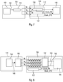
- a data packet 100 is generated in application logic 102 of a first integrated circuit (IC) 104, i.e. the transmitter IC, and is encoded and sent to a second IC 106, i.e. the receiver IC, via a data bus 108 having three data wires W 1 ...W 3 and without using a clock wire.
- the transmitter IC comprises a data transmission interface 110 which is arranged to generate three time-dependent binary (i.e. digital) signals V 1 ...V 3 which jointly encode the data packet. Each of the signals is associated with a unique data wire of the data bus 108.
- Each signal spans a temporal cycle of duration T within which are defined six consecutive time stamps T 1 ...T 6 at which the signals are allowed to change logical state, i.e. to change from a logical high state (or 1 state) to a logical low state (0 state) or vice versa.
- Each allowable set of the three time-dependent signals over a full cycle corresponds to a code word.
- the signals are transmitted to the receiver IC substantially in parallel on their respective data bus wires.
- the receiver IC comprises a data receiving interface 112 which is arranged to receive the signals from the transmitter interface via the data bus and decode the original data packet to provide a recovered data packet 114 to application logic 116 of the receiver IC.
- the data bus 108 could have more than one receiving IC connected to it, each of which is capable of monitoring the data bus and 'listening' for a specific addressing signal, for example. Therefore, whilst the embodiments described herein describe a first IC in communication with a second IC over a data bus, it is to be understood that the disclosure also extends to a first IC in communication with two or more ICs over a data bus.
- one or more ICs may have both a data transmission and a data receiving interface, as disclosed herein, such that said one or more ICs are capable of bi-directional communication of a data bus.
- data receiving and transmitting interfaces according to the present disclosure can be used in other devices/circuits, such as production testers and the like.
- Figure 2 illustrates an example code word representing a data packet being transmitted over the three wires of the data bus.
- the data encoding scheme at each time stamp T 1 ...T 6 exactly one of the signals changes logical state. In other words, at each time stamp T 1 ...T 6 one and only one of the three signals changes logical state.
- the encoding scheme guarantees that this is always the case, irrespective of the content of the data packet being transmitted over the data bus.
- each signal changes logical state twice during the cycle, again irrespective of the data packet content. This means that each signal begins and ends a cycle in the same logical state.
- the three signals all start the cycle in a logical low state and end the cycle in a logical low state. However, alternatively the three signals could all be in a logical high state at both the start and end of each cycle.
- all three signals change from a logical low state to a logical high state, or all three signals change from a logical high state to a logical low state.
- the second half of the cycle i.e. across time stamps T 4 ... T 6 all three signals change back to their initial state.
- time intervals ⁇ T between time stamps T 1 and T 2 ; T 2 and T 3 ; T 4 and T 5 ; and T 5 and T 6 are all substantially one twelfth of the cycle duration T.
- the time interval between time stamps T 3 and T 4 is one third of the cycle duration T. Therefore, a duration of one sixth the cycle duration Toccurs at the beginning and end of the cycle where no signal state changes occur, e.g. to act as a buffer between adjacent cycles. It should be appreciated that variations on these timing intervals may be made without departing from the scope of the present disclosure.
- the time interval between time stamps T 3 and T 4 is at least twice the time interval ⁇ T between the other time stamps, e.g. three or four times said time interval.
- the duration at the beginning and end of the cycle where no signal state changes occur is modified accordingly and, in general, the duration at the beginning of the cycle where no signal state changes occur will be the same as the duration at the end of the cycle where no signal state changes occur.
- ⁇ T is greater than 5% of the cycle duration T, e.g. one twelfth of the cycle duration.
- a data transfer capacity of the three-wire data bus of 5 bits per cycle can be achieved. This can be understood by considering the different combinations of signal state changes that can occur (i.e. code words) whilst still respecting the constraints set out above. For the rising or falling edges at T 1 ... T 3 there are six possible combinations. These are summarized in Table 1 below where e.g. row 1 of the table means that the signal on wire 1 changes state at T 1 , the signal on wire 2 changes at T 2 and the signal on wire 3 changes at T 3 . Table 1 T 1 T 2 T 3 W 1 W 2 W 3 W 1 W 3 W 2 W 1 W 3 W 2 W 3 W 1 W 3 W 1 W 2 W 3 W 2 W 1
- the data transfer capacity of the 3-wire data bus according to the present disclosure is 5 bits per cycle. This is greater than the capacity of 4 bits per cycle which is achievable using a serial peripheral interface when employing a dual data rate code, where one wire of the three-wire bus is dedicated for transmitting a clock signal and the other two wires are used as data wires.
- the 5-bit data packet 100 to be encoded and sent is first generated in application logic 102 of the transmitter IC 104, which does not generally form part of the data transmission interface.
- the 5-bit data packet to be transmitted in a given cycle is fed into a lookup table 118 which for each of the 32 possible 5-bit data packet stores signal state values (i.e. logical high or low) of the signals/wires for each of the time stamps T 1 ... T 6 .
- the data transmission interface may also include a clock generation circuit (not shown) arranged to generate the transmitter clock signal and trigger the flip-flops of the shift registers.
- the clock recovery circuit comprises a first XOR gate 124 which receives the three time-dependent binary signals and provides outputs to both a delay module 126 and a second XOR gate 128.
- the second XOR gate also receives, as its second input, the output of the delay module.
- the delay module delays the output of the first XOR gate by a constant time ⁇ which is generally a small fraction of the cycle duration. The precision of this delay is not critical because the receiver clock signal clock_RX generated with it is only used internally within the data receiving interface 112.
- the first XOR gate 124, second XOR gate 128 and delay module 126 are together arranged to generate the receiver clock signal clock_RX, which contains a clock edge or pulse at each of the time stamps T 1 ... T 6 .
- the clock recovery circuit 122 is further arranged to generate a system clock signal clock_SYS which contains exactly one clock pulse per cycle.
- the system clock signal is used by the application logic 116 of the receiver IC.
- the system clock signal may, for example, always have a rising edge at T 1 and always have a falling edge at T 4 , irrespective of the data packet content, and hence can provide a clean, reliable clock with a 50% duty cycle for use by the application logic.
- the clock recovery circuit 122 also comprises an OR gate 130, an AND gate 132, a third XOR gate 134 and a delay flip-flop 136, which together are arranged to generate the system clock signal.
- the first XOR gate 124 changes its output state every time one of its three input signals changes state. Hence, at each of the time stamps T 1 .. T 6 , this output changes its state.
- the output signal from the first XOR gate 124 and a delayed version of it are both fed to OR gate 128 which hence has its output at logic 1 in the time interval from a signal change of the output of first XOR gate 124 until the time interval ⁇ later. Then, the output of second XOR gate 128 stays at logic 0 until the next time stamp.
- the output of second XOR gate 128 hence has rising edges at each of the time stamps T 1 ... T 6 , and falling edges that occur a time ⁇ after each time stamp.
- the OR gate 130 has an output logic 1 in the whole time between T 1 and T 6 (as in this time interval, at least one of the signals is logic 1).
- the AND gate 132 has an output logic 1 in the whole time between T 3 and T 4 (as in this time interval, all three signals are logic 1).
- the output of the third XOR gate 134 is hence 1 between T 1 and T 3 , and between T 4 and T 6 . It has thus rising edges at T 1 and T 4 .
- Using this signal as a clock signal for the delay flip-flop 136 yields a clock signal clock_sys as shown in Figure 5 which illustrates exemplary receiver and system clock signals recovered in the clock recovery circuit 122 for an example set of three time-dependent binary signals received on wires W 1 ...W 3 .
- the receiver clock signal clock_RX has a clock pulse at each of the time stamps T 1 ... T 6 with the pulses each having a width ⁇ corresponding to the delay introduced by the delay module 126.
- the system clock signal clock_SYS has a rising edge at T 1 and a falling edge at T 4 .
- the receiver interface 112 forms part of a receiver IC 106 which may also include an application logic portion 116 which receives the recovered data packet 114 from the receiver interface as an input and performs some user-defined processing on it.
- the data receiving interface comprises a clock recovery circuit 122, such as that described above with reference to Figures 4 and 5 , in addition to a data recovery circuit 138.
- the incoming signals on data wires W 1 ...W 3 are sent to both the clock recovery circuit 122 and the data recovery circuit 138.
- the receiver clock signal clock_RX is fed from the clock recovery circuit to the data recovery circuit 138.
- the data recovery circuit comprises three 6-bit shift registers 140a, 140b, 140c, similar to the three 6-bit shift registers used in the data transmission interface. One shift register is associated with each data wire. The three shift registers are arranged to be populated with values corresponding to the logical states of the three signals at each of the time stamps T 1 ... T 6 . This is achieved by clocking the shift registers from the receiver clock signal clock_RX.
- the data recovery circuit further comprises a lookup table 142 which stores, for each possible 5-bit data packet, a set of values corresponding to the logical states of the three signals at each of the time stamps T 1 ... T 6 spanning the cycle.
- the lookup table is arranged to receive the output values of the three shift registers 140a, 140b, 140c and convert the values to provide a decoded/recovered data packet 114, e.g. for use by receiver application logic 116, which it will be appreciated generally falls outside of the data receiving interface according to the present disclosure.
- the lookup table is similar to that described above with reference to the data transmission interface
- Figure 7 is an overview of exemplary hardware for data transmission between two ICs over the 3-wire data bus according to an example embodiment.
- Such transmission from IC to IC is often used e.g. between a frontend IC sensing or receiving data, and a backend IC performing analysis of these data.
- Such transmission is also often used for system self-test in the field, where the application mode is interrupted in regular intervals and e.g. a CPU accesses analogue or mixed-signal instruments of another IC for verifying correct operation, e.g. using an IEEE 1687-compliant infrastructure.
- a first IC 104 comprises application logic 102 generating a data packet 100 which is encoded and transmitted, by the data transmission module 110, as three time-dependent binary signal over three data wires W 1 ...W 3 of a data bus, and without using a clock wire.
- the three signals are split between a clock recovery circuit 122 and a data recovery circuit 138 of a data receiving interface 112.
- the clock recovery circuit provides a receiver clock signal clock_RX, used by the data recovery circuit, and a system clock signal clock_SYS, used by application logic 116 of the second IC.
- the data recovery circuit decodes the three signals, using the receiver clock signal, to provide a decoded/recovered data packet 114 to the application logic 116 of the second IC.
- the present disclosure also covers the transmission from a production tester to an IC, such as a device under test (DUT), over a 3-wire data bus.
- a production tester to an IC, such as a device under test (DUT)
- DUT device under test
- This may be used to perform a scan test of ICs with limited pin count but where a high data rate is nevertheless desirable.
- a scan test is usually performed prior to device delivery using a production tester, a scan test may also be performed in the course of functional safety, e.g. during every start-up of a system containing the device.
- DFT scan test design for testing
- a transition test or a stuck-at test is transferred to the IC under test in an initialization sequence prior to transmission the actual scan patterns.
- a scan shift enable (SE) bit is often fed into the IC under test on a separate wire.
- SE scan shift enable
- typically 5 scan channels require 11 IC pins: 5 for scan in, 5 for scan out and 1 for SE.
- the SE bit can be generated internally within the IC under test and therefore it is advantageously possible to encode 11 internal scan bits (5 input, 1 scan control, 5 scan out) using only 6 external wires (3 input wires and 3 output wires).
- a production tester 143 generally consists of a pattern memory 144 and driver module 146 which receives scan data 148 from the pattern memory and transmits it to the IC under test over a three wire data bus W 1 ...W 3 .
- the scan data may already be processed to the code used, e.g. as described in Table 3, and stored in the pattern memory. Hence, it may not be necessary for the production tester to include a lookup table, e.g. in the driver module 146.
- the driver module 146 may include a lookup table for converting data from the pattern memory, encoding it according to the code used (e.g. of Table 3), and transmitting it over the 3-wire data bus to the IC under test. Otherwise the driver module may only include three 6-bit shift registers clocked by a transmitter clock signal as previously described.
- the IC under test 106 comprises a data receiving interface which is essentially the same as that described above, i.e. it includes a data recovery circuit 138 and a clock recovery circuit 122.
- the lookup table 142 of the data recovery circuit 138 is arranged to receive the outputs of the three 6-bit shift registers, in addition to the receiver clock signal clock_RX, and to provide two outputs: the retrieved scan_in data 150 and the SE bit 152. These are provided to the scan logic 154 within the IC under test. The scan logic is also provided with the system clock signal clock_SYS generated by the clock recovery circuit 122 in the manner previously described.
- Figure 9 illustrates further aspects of a production test setup according to the present disclosure.
- This includes scan data 148 creation on the production tester 143, transmission to the receiving IC using drivers 146, decoding in the receiving IC 106 being tested, then subsequent encoding of the scan output data and transferring them back to the production tester.
- the IC being tested further includes a data encoding circuit 156 which operates in a similar manner to the data transmission interface 110 described above.
- the data encoding circuit 156 receives a 5-bit data packet from the scan logic 154, representative of the recovered output scan data, and encodes and transmits it back to the production tester over a 3-wire data bus.
- the production tester further includes a set of comparators 158 which are arranged to compare the original scan data sent from the production tester to the IC under test with the recovered scan data sent back to the production tester from the IC under test.
- the above-described production test setup which effectively transfers 5 internal wires using 3 external bus wires, is independent of the specific test access and test control mechanisms being employed. It hence does not bundle JTAG connections and is not necessarily intended to convey JTAG control data.
- Figure 10 shares many elements in common with Figure 9 and like reference numerals are therefore used where appropriate.
- the IC under test 106 additionally includes a TAP controller 160.
- the same three data bus wires W 1 ...W 3 are used for transferring scan data and the TAP controller data from the production tester 143 to the IC under test 106.
- TAP controller stays in its programmed state once it has been programmed, i.e. that it is locked and can only be released from lock by a TAP controller reset command, e.g. code word 35 as per Table 3 above.
- code word 35 as per Table 3 above.
- the code word for TAP controller reset is not used.
- the scan_in 150 and SE signals 152 from the data recovery circuit 138 are gated appropriately using the TAP controller's control signals.
Landscapes
- Engineering & Computer Science (AREA)
- Physics & Mathematics (AREA)
- General Engineering & Computer Science (AREA)
- General Physics & Mathematics (AREA)
- Computer Networks & Wireless Communication (AREA)
- Signal Processing (AREA)
- Theoretical Computer Science (AREA)
- Spectroscopy & Molecular Physics (AREA)
- Health & Medical Sciences (AREA)
- Cardiology (AREA)
- General Health & Medical Sciences (AREA)
- Dc Digital Transmission (AREA)
Claims (15)
- Datenübertragungsschnittstelle (110) in einer ersten integrierten Schaltung (104), IC, zum Codieren und Senden eines Datenpakets (100) von der ersten IC an eine zweite IC (106) über einen Datenbus (108) mit drei Datendrähten (W1, W2, W3), wobei die Datenübertragungsschnittstelle ausgelegt ist, drei zeitabhängige binäre Signale (V1, V2, V3) zu erzeugen, die gemeinsam das Datenpaket codieren, wobei jedes der binären Signale einem eindeutigen Datendraht des Datenbusses zugeordnet ist und einen zeitlichen Zyklus T überspannt, innerhalb dessen sechs aufeinanderfolgende Zeitstempel T1, ..., T6 definiert sind, zu denen den binären Signalen erlaubt ist, den logischen Zustand zu wechseln, wobei die Datenübertragungsschnittstelle ferner ausgelegt ist, die binären Signale an die zweite IC im Wesentlichen gleichzeitig auf ihren jeweiligen Datendrähten zu senden, wobei ungeachtet des Datenpaketinhalts:zu jedem Zeitstempel T1, ..., T6 genau eines der binären Signale den logischen Zustand wechselt;jedes binäre Signal den logischen Zustand während des Zyklus zweimal wechselt; undin der ersten Hälfte des Zyklus T alle binären Signale von einem logisch tiefen Zustand zu einem logisch hohen Zustand wechseln oder alle binären Signale von einem logisch hohen Zustand zu einem logisch tiefen Zustand wechseln.
- Datenübertragungsschnittstelle nach Anspruch 1, die eine Nachschlagetabelle (118) umfasst, die ausgelegt ist, für jedes mögliche Datenpaket eine Gruppe von Werten zu speichern, die den logischen Zuständen der drei binären Signale zu jedem der Zeitstempel T1, ..., T6 entsprechen, wobei die Datenübertragungsschnittstelle ausgelegt ist, aus der Nachschlagetabelle die Gruppe von Werten, die dem Datenpaket entsprechen, zu bestimmen.
- Datenübertragungsschnittstelle nach Anspruch 2, die ferner drei 6-Bit-Schieberegister (120a, 120b, 120c) umfasst, wovon jedem binären Signal eines zugeordnet ist, wobei die Datenübertragungsschnittstelle ausgelegt ist, die Gruppe von Werten in das Schieberegister zu laden und danach die Gruppe von Werten gleichzeitig aus den Schieberegistern zu schieben, wodurch die drei zeitabhängigen binären Signale erzeugt werden.
- Datenübertragungsschnittstelle nach Anspruch 3, die ferner eine Takterzeugungsschaltung umfasst, die ausgelegt ist, ein Sendertaktsignal (clock_TX) zu erzeugen, das zu jedem der Zeitstempel T1, ..., T6 steigende oder fallende Flanken besitzt.
- Datenübertragungsschnittstelle nach Anspruch 4, wobei die Takterzeugungsschaltung ausgelegt ist, das Sendertaktsignal an das Schieberegister zu liefern, um die Gruppe von Werten gleichzeitig mit den Zeitstempeln T1, ..., T6 aus den drei Schieberegistern zu schieben.
- Datenempfangsschnittstelle (112) in einer zweiten integrierten Schaltung (106), IC, zum Empfangen und Decodieren eines Datenpakets (100), das von einer ersten IC (104) an die zweite IC über einen Datenbus mit drei Datendrähten (W1, W2, W3) gesendet wird, wobei die Datenempfangsschnittstelle ausgelegt ist, drei zeitabhängige binäre Signale (V1, V2, V3) zu empfangen, die gemeinsam das Datenpaket codieren, wobei jedes der binären Signale einem eindeutigen Draht des Datenbusses zugeordnet ist und einen zeitlichen Zyklus T überspannt, innerhalb dessen sechs aufeinanderfolgende Zeitstempel T1, ..., T6 definiert sind, zu denen den binären Signalen erlaubt ist, den logischen Zustand zu wechseln, wobei die Datenempfangsschnittstelle ferner ausgelegt ist, das Datenpaket von den drei binären Signalen zu decodieren, wobei ungeachtet des Datenpaketinhalts:zu jedem Zeitstempel T1, ..., T6 genau eines der binären Signale den logischen Zustand wechselt;jedes binäre Signal den logischen Zustand während des Zyklus zweimal wechselt; undin der ersten Hälfte des Zyklus T alle binären Signale von einem logisch tiefen Zustand zu einem logisch hohen Zustand wechseln oder alle binären Signale von einem logisch hohen Zustand zu einem logisch tiefen Zustand wechseln.
- Datenempfangsschnittstelle nach Anspruch 6, die eine Taktrückgewinnungsschaltung (122) umfasst, die ausgelegt ist, die drei binären Signale zu empfangen und ein Empfängertaktsignal (clock_RX) zu erzeugen, das zu jedem der Zeitstempel T1, ..., T6 eine Taktflanke oder einen Taktimpuls enthält.
- Datenempfangsschnittstelle nach Anspruch 7, wobei die Taktrückgewinnungsschaltung ein erstes XOR-Gate (124), ein zweites XOR-Gate (128) und ein Verzögerungsmodul (126) umfasst, die zusammen ausgelegt sind, das Empfängertaktsignal zu erzeugen.
- Datenempfangsschnittstelle nach Anspruch 7 oder 8, wobei die Taktrückgewinnungsschaltung ferner ausgelegt ist, ein Systemtaktsignal (clock_SYS) zu erzeugen, das genau einen Taktimpuls pro Zyklus T enthält.
- Datenempfangsschnittstelle nach einem der Ansprüche 7 bis 9, wobei die Datenempfangsschnittstelle ferner eine Datenrückgewinnungsschaltung (138) umfasst, die ausgelegt ist, das Empfängertaktsignal und die drei binären Signale zu empfangen und das Datenpaket daraus zu decodieren.
- Datenempfangsschnittstelle nach Anspruch 10, wobei die Datenrückgewinnungsschaltung drei 6-Bit-Schieberegister (140a, 140b, 140c) umfasst, wovon jedem binären Signal eines zugeordnet ist, wobei die drei Schieberegister ausgelegt sind, mit Werten bestückt zu werden, die den logischen Zuständen der drei binären Signale zu jedem der Zeitstempel T1, ..., T6 entsprechen, und ferner ausgelegt ist, von dem Empfängertaktsignal ausgelöst zu werden.
- Datenempfangsschnittstelle nach Anspruch 11, die ferner eine Nachschlagetabelle (142) umfasst, die ausgelegt ist, für jedes mögliche Datenpaket eine Gruppe von Werten zu speichern, die den logischen Zuständen der drei binären Signale zu jedem der Zeitstempel T1, ..., T6 entsprechen, die den Zyklus T überspannen, wobei die Nachschlagetabelle ausgelegt ist, die ausgegebenen Inhalte der Schieberegister zu empfangen und umzusetzen, um dadurch das Datenpaket zu decodieren.
- Datenüberragungs- oder Datenempfangsschnittstelle nach einem vorhergehenden Anspruch, wobei das Zeitintervall zwischen den Zeitstempeln T3 und T4 mindestens ein Viertel der Zyklusdauer, T-Dauer, vorzugsweise im Wesentlichen ein Drittel der Zyklusdauer, T-Dauer, beträgt.
- System, das Folgendes umfasst:eine erste Vorrichtung (104, 143) mit einer Datenübertragungsschnittstelle nach einem der Ansprüche 1 bis 5,eine zweite Vorrichtung (106) mit einer Datenempfangsschnittstelle nach einem der Ansprüche 6 bis 12; undeinen Datenbus (108) mit drei Datendrähten (W1, W2, W3), die zwischen der ersten Vorrichtung und der zweiten Vorrichtung angeschlossen sind.
- System nach Anspruch 14, wobei die erste Vorrichtung eine Produktionstesteinrichtung ist und die zweite Vorrichtung eine integrierte Schaltung, IC, unter Test ist, wobei die Produktionstesteinrichtung ausgelegt ist, einen Abtasttest der IC unter Test auszuführen.
Priority Applications (2)
| Application Number | Priority Date | Filing Date | Title |
|---|---|---|---|
| EP19171798.2A EP3734465B1 (de) | 2019-04-30 | 2019-04-30 | Datenübertragungscode und -schnittstelle |
| US16/837,368 US11145340B2 (en) | 2019-04-30 | 2020-04-01 | Data transmission code and interface |
Applications Claiming Priority (1)
| Application Number | Priority Date | Filing Date | Title |
|---|---|---|---|
| EP19171798.2A EP3734465B1 (de) | 2019-04-30 | 2019-04-30 | Datenübertragungscode und -schnittstelle |
Publications (2)
| Publication Number | Publication Date |
|---|---|
| EP3734465A1 EP3734465A1 (de) | 2020-11-04 |
| EP3734465B1 true EP3734465B1 (de) | 2021-11-03 |
Family
ID=66625733
Family Applications (1)
| Application Number | Title | Priority Date | Filing Date |
|---|---|---|---|
| EP19171798.2A Active EP3734465B1 (de) | 2019-04-30 | 2019-04-30 | Datenübertragungscode und -schnittstelle |
Country Status (2)
| Country | Link |
|---|---|
| US (1) | US11145340B2 (de) |
| EP (1) | EP3734465B1 (de) |
Families Citing this family (3)
| Publication number | Priority date | Publication date | Assignee | Title |
|---|---|---|---|---|
| CN111934707B (zh) * | 2019-04-25 | 2024-07-09 | 恩智浦有限公司 | 数据发射代码和接口 |
| US11005531B1 (en) * | 2020-04-13 | 2021-05-11 | Nxp B.V. | System and method for communicating over a single-wire transmission line |
| US11601136B2 (en) * | 2021-06-30 | 2023-03-07 | Bank Of America Corporation | System for electronic data compression by automated time-dependent compression algorithm |
Family Cites Families (12)
| Publication number | Priority date | Publication date | Assignee | Title |
|---|---|---|---|---|
| US6232796B1 (en) | 1999-07-21 | 2001-05-15 | Rambus Incorporated | Apparatus and method for detecting two data bits per clock edge |
| US6934898B1 (en) | 2001-11-30 | 2005-08-23 | Koninklijke Philips Electronics N.V. | Test circuit topology reconfiguration and utilization techniques |
| US6809664B1 (en) | 2003-06-26 | 2004-10-26 | International Business Machines Corporation | Double width data bus, single rate to single width data bus, double rate converter circuit |
| US7103110B2 (en) * | 2003-10-10 | 2006-09-05 | Atmel Corporation | Dual phase pulse modulation encoder circuit |
| US7818641B2 (en) | 2006-10-18 | 2010-10-19 | Texas Instruments Incorporated | Interface to full and reduce pin JTAG devices |
| US8046651B2 (en) | 2008-04-02 | 2011-10-25 | Texas Instruments Incorporated | Compare circuit receiving scan register and inverted clock flip-flop data |
| TWI443557B (zh) * | 2010-09-30 | 2014-07-01 | Wintek Corp | 觸控面板資料傳輸方法 |
| WO2013088173A1 (en) * | 2011-12-14 | 2013-06-20 | Wolfson Microelectronics Plc | Data transfer |
| US10289600B2 (en) * | 2013-08-08 | 2019-05-14 | Qualcomm Incorporated | Reducing transmitter encoding jitter in a C-PHY interface using multiple clock phases to launch symbols |
| CN104425037B (zh) | 2013-08-19 | 2019-07-12 | 恩智浦美国有限公司 | 可重配置电路及其解码器 |
| US10571518B1 (en) | 2018-09-26 | 2020-02-25 | Nxp B.V. | Limited pin test interface with analog test bus |
| CN111934707B (zh) * | 2019-04-25 | 2024-07-09 | 恩智浦有限公司 | 数据发射代码和接口 |
-
2019
- 2019-04-30 EP EP19171798.2A patent/EP3734465B1/de active Active
-
2020
- 2020-04-01 US US16/837,368 patent/US11145340B2/en active Active
Also Published As
| Publication number | Publication date |
|---|---|
| US11145340B2 (en) | 2021-10-12 |
| US20200349988A1 (en) | 2020-11-05 |
| EP3734465A1 (de) | 2020-11-04 |
Similar Documents
| Publication | Publication Date | Title |
|---|---|---|
| US9735950B1 (en) | Burst mode clock data recovery circuit for MIPI C-PHY receivers | |
| US8726112B2 (en) | Scan test application through high-speed serial input/outputs | |
| US7936684B2 (en) | Physical layer loopback | |
| US6977981B2 (en) | Method and apparatus for reducing power requirements in a multi gigabit parallel to serial converter | |
| US9702935B2 (en) | Packet based integrated circuit testing | |
| US20060107154A1 (en) | Through-core self-test with multiple loopbacks | |
| US8464145B2 (en) | Serial interface devices, systems and methods | |
| US11145340B2 (en) | Data transmission code and interface | |
| US7058535B2 (en) | Test system for integrated circuits with serdes ports | |
| US20080235405A1 (en) | USB controller and a testing method of the USB controller | |
| US7882474B2 (en) | Testing phase error of multiple on-die clocks | |
| US7920079B2 (en) | Serial signal receiving device, serial transmission system and serial transmission method | |
| US6892337B1 (en) | Circuit and method for testing physical layer functions of a communication network | |
| CN107947873A (zh) | 具有多个传输通道的数据传输系统及测试传输数据的方法 | |
| US10565156B1 (en) | Wired-data bus transmission using signal transition coding | |
| US11169952B2 (en) | Data transmission code and interface | |
| US11609872B2 (en) | Integrated circuit having lanes interchangeable between clock and data lanes in clock forward interface receiver | |
| US20030223522A1 (en) | Bit synchronizing circuit | |
| WO2022266959A1 (zh) | 一种芯片测试电路和方法 | |
| US7165196B1 (en) | Method for testing serializers/de-serializers | |
| US11012087B2 (en) | Encoding and decoding architecture for high speed data communication system and related physical layer circuit, transmitter and receiver and communication system thereof | |
| JP3021855B2 (ja) | シリアルデータ転送装置 | |
| Upadhyay et al. | Scan SerDes* for multi-die packages | |
| US20260095205A1 (en) | Single wire serial interface and protocol for intra-chip communications | |
| US20250283940A1 (en) | Method, system and device of serializing and de-serializing the delivery of scan test data through chip i/o to reduce the scan test duration of an integrated circuit |
Legal Events
| Date | Code | Title | Description |
|---|---|---|---|
| PUAI | Public reference made under article 153(3) epc to a published international application that has entered the european phase |
Free format text: ORIGINAL CODE: 0009012 |
|
| STAA | Information on the status of an ep patent application or granted ep patent |
Free format text: STATUS: THE APPLICATION HAS BEEN PUBLISHED |
|
| AK | Designated contracting states |
Kind code of ref document: A1 Designated state(s): AL AT BE BG CH CY CZ DE DK EE ES FI FR GB GR HR HU IE IS IT LI LT LU LV MC MK MT NL NO PL PT RO RS SE SI SK SM TR |
|
| AX | Request for extension of the european patent |
Extension state: BA ME |
|
| STAA | Information on the status of an ep patent application or granted ep patent |
Free format text: STATUS: REQUEST FOR EXAMINATION WAS MADE |
|
| 17P | Request for examination filed |
Effective date: 20210504 |
|
| RBV | Designated contracting states (corrected) |
Designated state(s): AL AT BE BG CH CY CZ DE DK EE ES FI FR GB GR HR HU IE IS IT LI LT LU LV MC MK MT NL NO PL PT RO RS SE SI SK SM TR |
|
| GRAP | Despatch of communication of intention to grant a patent |
Free format text: ORIGINAL CODE: EPIDOSNIGR1 |
|
| STAA | Information on the status of an ep patent application or granted ep patent |
Free format text: STATUS: GRANT OF PATENT IS INTENDED |
|
| INTG | Intention to grant announced |
Effective date: 20210618 |
|
| GRAS | Grant fee paid |
Free format text: ORIGINAL CODE: EPIDOSNIGR3 |
|
| GRAA | (expected) grant |
Free format text: ORIGINAL CODE: 0009210 |
|
| STAA | Information on the status of an ep patent application or granted ep patent |
Free format text: STATUS: THE PATENT HAS BEEN GRANTED |
|
| AK | Designated contracting states |
Kind code of ref document: B1 Designated state(s): AL AT BE BG CH CY CZ DE DK EE ES FI FR GB GR HR HU IE IS IT LI LT LU LV MC MK MT NL NO PL PT RO RS SE SI SK SM TR |
|
| REG | Reference to a national code |
Ref country code: GB Ref legal event code: FG4D |
|
| REG | Reference to a national code |
Ref country code: AT Ref legal event code: REF Ref document number: 1444598 Country of ref document: AT Kind code of ref document: T Effective date: 20211115 Ref country code: CH Ref legal event code: EP |
|
| REG | Reference to a national code |
Ref country code: IE Ref legal event code: FG4D |
|
| REG | Reference to a national code |
Ref country code: DE Ref legal event code: R096 Ref document number: 602019008830 Country of ref document: DE |
|
| REG | Reference to a national code |
Ref country code: LT Ref legal event code: MG9D |
|
| REG | Reference to a national code |
Ref country code: NL Ref legal event code: MP Effective date: 20211103 |
|
| REG | Reference to a national code |
Ref country code: AT Ref legal event code: MK05 Ref document number: 1444598 Country of ref document: AT Kind code of ref document: T Effective date: 20211103 |
|
| PG25 | Lapsed in a contracting state [announced via postgrant information from national office to epo] |
Ref country code: RS Free format text: LAPSE BECAUSE OF FAILURE TO SUBMIT A TRANSLATION OF THE DESCRIPTION OR TO PAY THE FEE WITHIN THE PRESCRIBED TIME-LIMIT Effective date: 20211103 Ref country code: LT Free format text: LAPSE BECAUSE OF FAILURE TO SUBMIT A TRANSLATION OF THE DESCRIPTION OR TO PAY THE FEE WITHIN THE PRESCRIBED TIME-LIMIT Effective date: 20211103 Ref country code: FI Free format text: LAPSE BECAUSE OF FAILURE TO SUBMIT A TRANSLATION OF THE DESCRIPTION OR TO PAY THE FEE WITHIN THE PRESCRIBED TIME-LIMIT Effective date: 20211103 Ref country code: BG Free format text: LAPSE BECAUSE OF FAILURE TO SUBMIT A TRANSLATION OF THE DESCRIPTION OR TO PAY THE FEE WITHIN THE PRESCRIBED TIME-LIMIT Effective date: 20220203 Ref country code: AT Free format text: LAPSE BECAUSE OF FAILURE TO SUBMIT A TRANSLATION OF THE DESCRIPTION OR TO PAY THE FEE WITHIN THE PRESCRIBED TIME-LIMIT Effective date: 20211103 |
|
| PG25 | Lapsed in a contracting state [announced via postgrant information from national office to epo] |
Ref country code: IS Free format text: LAPSE BECAUSE OF FAILURE TO SUBMIT A TRANSLATION OF THE DESCRIPTION OR TO PAY THE FEE WITHIN THE PRESCRIBED TIME-LIMIT Effective date: 20220303 Ref country code: SE Free format text: LAPSE BECAUSE OF FAILURE TO SUBMIT A TRANSLATION OF THE DESCRIPTION OR TO PAY THE FEE WITHIN THE PRESCRIBED TIME-LIMIT Effective date: 20211103 Ref country code: PT Free format text: LAPSE BECAUSE OF FAILURE TO SUBMIT A TRANSLATION OF THE DESCRIPTION OR TO PAY THE FEE WITHIN THE PRESCRIBED TIME-LIMIT Effective date: 20220303 Ref country code: PL Free format text: LAPSE BECAUSE OF FAILURE TO SUBMIT A TRANSLATION OF THE DESCRIPTION OR TO PAY THE FEE WITHIN THE PRESCRIBED TIME-LIMIT Effective date: 20211103 Ref country code: NO Free format text: LAPSE BECAUSE OF FAILURE TO SUBMIT A TRANSLATION OF THE DESCRIPTION OR TO PAY THE FEE WITHIN THE PRESCRIBED TIME-LIMIT Effective date: 20220203 Ref country code: NL Free format text: LAPSE BECAUSE OF FAILURE TO SUBMIT A TRANSLATION OF THE DESCRIPTION OR TO PAY THE FEE WITHIN THE PRESCRIBED TIME-LIMIT Effective date: 20211103 Ref country code: LV Free format text: LAPSE BECAUSE OF FAILURE TO SUBMIT A TRANSLATION OF THE DESCRIPTION OR TO PAY THE FEE WITHIN THE PRESCRIBED TIME-LIMIT Effective date: 20211103 Ref country code: HR Free format text: LAPSE BECAUSE OF FAILURE TO SUBMIT A TRANSLATION OF THE DESCRIPTION OR TO PAY THE FEE WITHIN THE PRESCRIBED TIME-LIMIT Effective date: 20211103 Ref country code: GR Free format text: LAPSE BECAUSE OF FAILURE TO SUBMIT A TRANSLATION OF THE DESCRIPTION OR TO PAY THE FEE WITHIN THE PRESCRIBED TIME-LIMIT Effective date: 20220204 Ref country code: ES Free format text: LAPSE BECAUSE OF FAILURE TO SUBMIT A TRANSLATION OF THE DESCRIPTION OR TO PAY THE FEE WITHIN THE PRESCRIBED TIME-LIMIT Effective date: 20211103 |
|
| PG25 | Lapsed in a contracting state [announced via postgrant information from national office to epo] |
Ref country code: SM Free format text: LAPSE BECAUSE OF FAILURE TO SUBMIT A TRANSLATION OF THE DESCRIPTION OR TO PAY THE FEE WITHIN THE PRESCRIBED TIME-LIMIT Effective date: 20211103 Ref country code: SK Free format text: LAPSE BECAUSE OF FAILURE TO SUBMIT A TRANSLATION OF THE DESCRIPTION OR TO PAY THE FEE WITHIN THE PRESCRIBED TIME-LIMIT Effective date: 20211103 Ref country code: RO Free format text: LAPSE BECAUSE OF FAILURE TO SUBMIT A TRANSLATION OF THE DESCRIPTION OR TO PAY THE FEE WITHIN THE PRESCRIBED TIME-LIMIT Effective date: 20211103 Ref country code: EE Free format text: LAPSE BECAUSE OF FAILURE TO SUBMIT A TRANSLATION OF THE DESCRIPTION OR TO PAY THE FEE WITHIN THE PRESCRIBED TIME-LIMIT Effective date: 20211103 Ref country code: DK Free format text: LAPSE BECAUSE OF FAILURE TO SUBMIT A TRANSLATION OF THE DESCRIPTION OR TO PAY THE FEE WITHIN THE PRESCRIBED TIME-LIMIT Effective date: 20211103 Ref country code: CZ Free format text: LAPSE BECAUSE OF FAILURE TO SUBMIT A TRANSLATION OF THE DESCRIPTION OR TO PAY THE FEE WITHIN THE PRESCRIBED TIME-LIMIT Effective date: 20211103 |
|
| REG | Reference to a national code |
Ref country code: DE Ref legal event code: R097 Ref document number: 602019008830 Country of ref document: DE |
|
| PLBE | No opposition filed within time limit |
Free format text: ORIGINAL CODE: 0009261 |
|
| STAA | Information on the status of an ep patent application or granted ep patent |
Free format text: STATUS: NO OPPOSITION FILED WITHIN TIME LIMIT |
|
| 26N | No opposition filed |
Effective date: 20220804 |
|
| PG25 | Lapsed in a contracting state [announced via postgrant information from national office to epo] |
Ref country code: AL Free format text: LAPSE BECAUSE OF FAILURE TO SUBMIT A TRANSLATION OF THE DESCRIPTION OR TO PAY THE FEE WITHIN THE PRESCRIBED TIME-LIMIT Effective date: 20211103 |
|
| PG25 | Lapsed in a contracting state [announced via postgrant information from national office to epo] |
Ref country code: SI Free format text: LAPSE BECAUSE OF FAILURE TO SUBMIT A TRANSLATION OF THE DESCRIPTION OR TO PAY THE FEE WITHIN THE PRESCRIBED TIME-LIMIT Effective date: 20211103 |
|
| REG | Reference to a national code |
Ref country code: CH Ref legal event code: PL |
|
| REG | Reference to a national code |
Ref country code: BE Ref legal event code: MM Effective date: 20220430 |
|
| PG25 | Lapsed in a contracting state [announced via postgrant information from national office to epo] |
Ref country code: MC Free format text: LAPSE BECAUSE OF FAILURE TO SUBMIT A TRANSLATION OF THE DESCRIPTION OR TO PAY THE FEE WITHIN THE PRESCRIBED TIME-LIMIT Effective date: 20211103 Ref country code: LU Free format text: LAPSE BECAUSE OF NON-PAYMENT OF DUE FEES Effective date: 20220430 Ref country code: LI Free format text: LAPSE BECAUSE OF NON-PAYMENT OF DUE FEES Effective date: 20220430 Ref country code: FR Free format text: LAPSE BECAUSE OF NON-PAYMENT OF DUE FEES Effective date: 20220430 Ref country code: CH Free format text: LAPSE BECAUSE OF NON-PAYMENT OF DUE FEES Effective date: 20220430 |
|
| PG25 | Lapsed in a contracting state [announced via postgrant information from national office to epo] |
Ref country code: BE Free format text: LAPSE BECAUSE OF NON-PAYMENT OF DUE FEES Effective date: 20220430 |
|
| PG25 | Lapsed in a contracting state [announced via postgrant information from national office to epo] |
Ref country code: IE Free format text: LAPSE BECAUSE OF NON-PAYMENT OF DUE FEES Effective date: 20220430 |
|
| PG25 | Lapsed in a contracting state [announced via postgrant information from national office to epo] |
Ref country code: IT Free format text: LAPSE BECAUSE OF FAILURE TO SUBMIT A TRANSLATION OF THE DESCRIPTION OR TO PAY THE FEE WITHIN THE PRESCRIBED TIME-LIMIT Effective date: 20211103 |
|
| P01 | Opt-out of the competence of the unified patent court (upc) registered |
Effective date: 20230725 |
|
| GBPC | Gb: european patent ceased through non-payment of renewal fee |
Effective date: 20230430 |
|
| PG25 | Lapsed in a contracting state [announced via postgrant information from national office to epo] |
Ref country code: GB Free format text: LAPSE BECAUSE OF NON-PAYMENT OF DUE FEES Effective date: 20230430 |
|
| PG25 | Lapsed in a contracting state [announced via postgrant information from national office to epo] |
Ref country code: GB Free format text: LAPSE BECAUSE OF NON-PAYMENT OF DUE FEES Effective date: 20230430 |
|
| PG25 | Lapsed in a contracting state [announced via postgrant information from national office to epo] |
Ref country code: MK Free format text: LAPSE BECAUSE OF FAILURE TO SUBMIT A TRANSLATION OF THE DESCRIPTION OR TO PAY THE FEE WITHIN THE PRESCRIBED TIME-LIMIT Effective date: 20211103 Ref country code: CY Free format text: LAPSE BECAUSE OF FAILURE TO SUBMIT A TRANSLATION OF THE DESCRIPTION OR TO PAY THE FEE WITHIN THE PRESCRIBED TIME-LIMIT Effective date: 20211103 |
|
| PG25 | Lapsed in a contracting state [announced via postgrant information from national office to epo] |
Ref country code: HU Free format text: LAPSE BECAUSE OF FAILURE TO SUBMIT A TRANSLATION OF THE DESCRIPTION OR TO PAY THE FEE WITHIN THE PRESCRIBED TIME-LIMIT; INVALID AB INITIO Effective date: 20190430 |
|
| PG25 | Lapsed in a contracting state [announced via postgrant information from national office to epo] |
Ref country code: MT Free format text: LAPSE BECAUSE OF FAILURE TO SUBMIT A TRANSLATION OF THE DESCRIPTION OR TO PAY THE FEE WITHIN THE PRESCRIBED TIME-LIMIT Effective date: 20211103 |
|
| PGFP | Annual fee paid to national office [announced via postgrant information from national office to epo] |
Ref country code: DE Payment date: 20250319 Year of fee payment: 7 |
|
| PG25 | Lapsed in a contracting state [announced via postgrant information from national office to epo] |
Ref country code: TR Free format text: LAPSE BECAUSE OF FAILURE TO SUBMIT A TRANSLATION OF THE DESCRIPTION OR TO PAY THE FEE WITHIN THE PRESCRIBED TIME-LIMIT Effective date: 20211103 |