EP3735710B1 - Robuste quantenlogikgatter - Google Patents
Robuste quantenlogikgatter Download PDFInfo
- Publication number
- EP3735710B1 EP3735710B1 EP19751562.0A EP19751562A EP3735710B1 EP 3735710 B1 EP3735710 B1 EP 3735710B1 EP 19751562 A EP19751562 A EP 19751562A EP 3735710 B1 EP3735710 B1 EP 3735710B1
- Authority
- EP
- European Patent Office
- Prior art keywords
- cavity
- transmon
- cps
- ancilla
- swap
- Prior art date
- Legal status (The legal status is an assumption and is not a legal conclusion. Google has not performed a legal analysis and makes no representation as to the accuracy of the status listed.)
- Active
Links
Images



Classifications
-
- G—PHYSICS
- G06—COMPUTING OR CALCULATING; COUNTING
- G06N—COMPUTING ARRANGEMENTS BASED ON SPECIFIC COMPUTATIONAL MODELS
- G06N10/00—Quantum computing, i.e. information processing based on quantum-mechanical phenomena
- G06N10/20—Models of quantum computing, e.g. quantum circuits or universal quantum computers
-
- G—PHYSICS
- G06—COMPUTING OR CALCULATING; COUNTING
- G06N—COMPUTING ARRANGEMENTS BASED ON SPECIFIC COMPUTATIONAL MODELS
- G06N10/00—Quantum computing, i.e. information processing based on quantum-mechanical phenomena
- G06N10/40—Physical realisations or architectures of quantum processors or components for manipulating qubits, e.g. qubit coupling or qubit control
-
- G—PHYSICS
- G06—COMPUTING OR CALCULATING; COUNTING
- G06N—COMPUTING ARRANGEMENTS BASED ON SPECIFIC COMPUTATIONAL MODELS
- G06N10/00—Quantum computing, i.e. information processing based on quantum-mechanical phenomena
- G06N10/70—Quantum error correction, detection or prevention, e.g. surface codes or magic state distillation
-
- H—ELECTRICITY
- H01—ELECTRIC ELEMENTS
- H01P—WAVEGUIDES; RESONATORS, LINES, OR OTHER DEVICES OF THE WAVEGUIDE TYPE
- H01P5/00—Coupling devices of the waveguide type
- H01P5/12—Coupling devices having more than two ports
- H01P5/16—Conjugate devices, i.e. devices having at least one port decoupled from one other port
- H01P5/18—Conjugate devices, i.e. devices having at least one port decoupled from one other port consisting of two coupled guides, e.g. directional couplers
-
- H—ELECTRICITY
- H03—ELECTRONIC CIRCUITRY
- H03K—PULSE TECHNIQUE
- H03K19/00—Logic circuits, i.e. having at least two inputs acting on one output; Inverting circuits
- H03K19/02—Logic circuits, i.e. having at least two inputs acting on one output; Inverting circuits using specified components
- H03K19/195—Logic circuits, i.e. having at least two inputs acting on one output; Inverting circuits using specified components using superconductive devices
-
- H—ELECTRICITY
- H10—SEMICONDUCTOR DEVICES; ELECTRIC SOLID-STATE DEVICES NOT OTHERWISE PROVIDED FOR
- H10N—ELECTRIC SOLID-STATE DEVICES NOT OTHERWISE PROVIDED FOR
- H10N60/00—Superconducting devices
- H10N60/10—Junction-based devices
-
- B—PERFORMING OPERATIONS; TRANSPORTING
- B82—NANOTECHNOLOGY
- B82Y—SPECIFIC USES OR APPLICATIONS OF NANOSTRUCTURES; MEASUREMENT OR ANALYSIS OF NANOSTRUCTURES; MANUFACTURE OR TREATMENT OF NANOSTRUCTURES
- B82Y10/00—Nanotechnology for information processing, storage or transmission, e.g. quantum computing or single electron logic
-
- H—ELECTRICITY
- H10—SEMICONDUCTOR DEVICES; ELECTRIC SOLID-STATE DEVICES NOT OTHERWISE PROVIDED FOR
- H10N—ELECTRIC SOLID-STATE DEVICES NOT OTHERWISE PROVIDED FOR
- H10N60/00—Superconducting devices
- H10N60/10—Junction-based devices
- H10N60/12—Josephson-effect devices
Definitions
- Quantum information processing uses quantum mechanical phenomena, such as energy quantization, superposition, and entanglement, to encode and process information in a way not utilized by conventional information processing. For example, it is known that certain computational problems may be solved more efficiently using quantum computation rather than conventional classical computation.
- quantum computation requires the ability to precisely control a large number of quantum bits, known as "qubits," and the interactions between these qubits.
- qubits should have long coherence times, be able to be individually manipulated, be able to interact with one or more other qubits to implement multi-qubit gates, be able to be initialized and measured efficiently, and be scalable to large numbers of qubits.
- a qubit may be formed from any physical quantum mechanical system with at least two orthogonal states.
- the two states of the system used to encode information are referred to as the "computational basis.”
- photon polarization, electron spin, and nuclear spin are two-level systems that may encode information and may therefore be used as a qubit for quantum information processing.
- Different physical implementations of qubits have different advantages and disadvantages. For example, photon polarization benefits from long coherence times and simple single qubit manipulation, but suffers from the inability to create simple multi-qubit gates.
- phase qubits where the computational basis is the quantized energy states of Cooper pairs in a Josephson Junction
- flux qubits where the computational basis is the direction of circulating current flow in a superconducting loop
- charge qubits where the computational basis is the presence or absence of a Cooper pair on a superconducting island.
- superconducting qubits are an advantageous choice of qubit because the coupling between two qubits is strong making two-qubit gates relatively simple to implement, and superconducting qubits are scalable because they are mesoscopic components that may be formed using conventional electronic circuitry techniques.
- superconducting qubits exhibit excellent quantum coherence and a strong non-linearity associated with the Josephson effect. All superconducting qubit designs use at least one Josephson junction as a non-linear non-dissipative element.
- Article entitled " New Class of Quantum Error-Correcting Codes for a Bosonic Mode" from Marios H. Michael et al. (Physical Review X, vol. 6, no. 3, 29 January 2016 ) disclose examples of quantum error-correcting solutions.
- a method is provided as defined by the independent claim 1.
- a multi-cavity quantum information system is provided as defined by the independent claim 11.
- the dependent claims specify preferred embodiments.
- the information is stored in Josephson-junction based qubits (e.g., transmons) coupled together via exchange of microwave photons in bus resonators or via direct capacitive coupling.
- Josephson-junction based qubits e.g., transmons
- the inventors have recognized and appreciated that a different and complementary architecture in which the quantum information is stored and manipulated in microwave photon states of high-Q resonators with transmons acting as ancillae to give universal quantum control of the photonic qubits has significant advantages over the conventional approaches.
- coherence times of microwave cavities are longer than coherence times of superconducting qubits.
- three-dimensional superconducting microwave cavities can achieve extremely high quality factors approaching 109 in aluminum, and still higher in niobium, with cavity coherence times for aluminum cavities exceeding that of the transmon by two orders of magnitude.
- the number of states in which information can be encoded is larger in a microwave cavity than in a superconducting qubit.
- the higher excitation levels of the cavity mode expand the available Hilbert space so that a single cavity mode can be used to encode quantum bits of information in a manner compatible with quantum error correction against various imperfections, including cavity dephasing, excitation loss or thermal heating.
- microwave cavities can be utilized in a unique approach to quantum information processing where quantum information is stored in the quantum state of a microwave cavity while using the transmon as an ancilla to assist quantum information processing and quantum error correction.
- This 'photonic qubit' approach is the reverse of the conventional approach in which quantum information is stored in the transmons and microwave photon modes are used as quantum busses to couple the transmons.
- the resulting superconducting cavity-transmon system allows universal quantum control over the cavity mode, quantum error correction reaching the break-even point, joint parity measurement over two cavities, and deterministic coupling gates between the cavities assisted by a transmon controller.
- the inventors have further recognized and appreciated that the superconducting cavity-transmon system may encounter limited fidelity of quantum operations, due to the transmon decoherence during the cavity-transmon coupling.
- the inventors have recognized and appreciated that, besides experimentally improving the coherence properties of the transmon, the fidelity of quantum operations can be improved by implementing robust approaches to suppress or even actively correct the errors due to the decoherence from transmon and other Josephson nonlinear devices.
- the inventors have further recognized and appreciated that the universal set of quantum logic gates are "encoding agnostic," meaning no matter how the quantum information is chosen to be logically encoded in the quantum state of the cavity (e.g., cat state encoding, coherent state encoding, Fock state encoding, etc.), the set of quantum logic gates remains universal. Moreover, the hardware used to implement the universal set of quantum logic gates remains the same, independent of the chosen encoding scheme.
- multiple microwave cavities are controlled and/or coupled together using one or more Josephson nonlinear devices such as a transmons.
- a coupling transmon is used to perform operations between two cavities. Examples of such operations include beam splitter (BS) operations that couple the quantum state of a first cavity to the quantum state of a second cavity and vice versa. These operations are referred to as beam splitter operations because they play the same role and implement the same unitary operation as beam splitters do in linear optics quantum computation (LOQC) schemes.
- BS beam splitter
- LOQC linear optics quantum computation
- an ancilla transmon that is coupled to a single cavity is used to implement controlled phase shift (CPS) operations between the single cavity and the transmon.
- the ancilla transmon may also be controlled to implement rotations on the quantum state of the ancilla transmon itself.
- the inventors have recognized and appreciated that the BS operations, CPS operations, and rotations of the ancilla transmon are sufficient to implement universal gate based quantum computation.
- the above operations are used to implement c-SWAP and/or e-SWAP gates.
- the e-SWAP gate couples cavity modes while preserving the bosonic code space. In this way, entangling operations between bosonic modes can be achieved regardless of the logical encoding used.
- Some embodiments utilize a robust design of the e-SWAP gate that can herald imperfections due to transmon decoherence.
- Some embodiments utilized the c-SWAP and e-SWAP gates for one or more applications, such as quantum routers, quantum random access memory (RAM), quantum principle component analysis, and gate-based universal quantum computation.
- transmon superconducting qubit is described herein as a component of multiple embodiments, other types of superconducting devices may be used in some embodiments.
- FIG. 1 is a schematic diagram of a multi-cavity quantum information system 100, according to some embodiments.
- the multi-cavity quantum information system 100 includes a first cavity 101, a second cavity 102, a coupling transmon 103, a first ancilla transmon 104, a second ancilla transmon 105 and a microwave source 106. While only two cavities and two ancilla transmon are shown in the example system 100 of FIG. 1 , other embodiment may include additional cavities and transmons.
- the first cavity 101 and the second cavity 102 may be any type of cavity that supports quantum states of microwave radiation.
- the first cavity 101 and the second cavity 102 may be a transmission line resonator or a three-dimensional cavity formed from a superconducting material, such as aluminum.
- the coupling transmon 103 may be a transmon that is dispersively coupled to both the first cavity 101 and the second cavity 102.
- the coupling transmon 103 provides an interaction between the quantum states of the two cavities, allowing for interactions such as BS interactions to be performed between the first cavity 101 and the second cavity 102.
- the first ancilla transmon 104 and the second ancilla transmon 105 are dispersively coupled to the first cavity 101 and the second cavity 102, respectively.
- Each ancilla transmon is coupled to a single cavity of the system 100 and not to any other cavity used to store quantum information.
- the ancilla transmons 104 and 105 can be controlled to implement rotations of the quantum state of the transmons 104 and 105 themselves. Additionally, the ancilla transmons 104 and 105 can be controlled to interact with the associated cavities 101 and 102, respectively, to implement controlled interactions such as a CPS interaction.
- the microwave source 106 may be coupled to the first cavity 101, the second cavity 102, the first ancilla transmon 104, the second ancilla transmon 105, and the coupling transmon 103.
- the coupling between the microwave source 106 and the other components provides a way for the microwave source to apply microwave radiation to each of the components of the multi-cavity quantum information system 100.
- the microwave source 106 may be capacitively coupled to each of the components.
- FIG. 1B is a schematic diagram of a particular example system 110 that may play the role of the multi-cavity quantum information system 100 of FIG. 1A (for simplicity the microwave source 106 is not shown), according to some embodiments.
- the system 110 includes a first three-dimensional (3D) cavity 111, a second 3D cavity 121, a coupling device 131, a first ancilla device 141, and a second ancilla device 151.
- 3D three-dimensional
- the central stub 114 may have a height of 4.8 mm and the second central stub 124 may have a height of 5.6 mm.
- the first 3D cavity 111 supports microwave radiation 112 of a first frequency and the second 3D cavity 121 supports microwave radiation 122 of a second frequency that is different from the first frequency.
- the first cavity 111 and the second cavity 121 include ports 113 and 123, respectively, through which microwave radiation from the microwave source 106 may be applied. Applying microwave radiation to a cavity may, for example, implement a displacement operation on the quantum state of the cavity.
- the nonlinearity of the transmon 134 of the coupling device 131 enables four wave mixing, which is used to perform a frequency-converting bilinear coupling between the first cavity 111 an the second cavity 121.
- additional nonlinear elements may be used to facilitate quantum information processing.
- using the physical platform of superconducting circuits with microwave photons not only provides the capabilities of single-photon sources and photon detectors, but also includes at least one highly controllable transmon that can be used as two-level or multi-level ancillae.
- quantum operations that combine the beam splitter unitary operator and cavity-transmon dispersive coupling gates are used to perform quantum information processing operations.
- the dispersive coupling gates are still linear optics transformations that are controlled by (e.g., based upon and/or conditioned on) the quantum state of a transmon (or other) ancilla.
- First ancilla device 141 is similar to the coupling device 131, but only couples to a the first cavity 111, not both cavities.
- the first ancilla device includes a pump port 142 for driving a transmon 144 with pump and readout pulses of microwave radiation and a readout port 143 for receiving readout microwave signals from the transmon 144.
- the transmon 144 is coupled to the first cavity 111 via a first antenna pad 145 that at least partially protrudes into the first cavity 111.
- a second antenna pad 146 couples the transmon 144 to a quasi-planar resonator 147.
- the second ancilla device 151 is similar to the first ancilla device 141, but is coupled to only the second cavity 121, not the first cavity 111.
- the second ancilla device includes a pump port 152 for driving a transmon 154 with pump and readout pulses of microwave radiation and a readout port 153 for receiving readout microwave signals from the transmon 154.
- the transmon 154 is coupled to the first cavity 111 via a first antenna pad 155 that at least partially protrudes into the first cavity 111.
- a second antenna pad 156 couples the transmon 144 to a quasi-planar resonator 147.
- ⁇ n ⁇ for a time duration t ⁇ / ⁇ and coupling strength ⁇ .
- a c-SWAP gate is implemented using a combination of BS operations and CPS operations.
- a c-SWAP gate operates on two cavity modes and one of the ancilla transmons, swapping the states of the two cavities based on the state of the ancilla transmon.
- ⁇ SWAP where
- e ⁇ represent the ground state and the first excited state of the ancilla transmon, respectively. Because (c-SWAP) 2 I , c-SWAP is reversible.
- the c-SWAP gate is sometimes called the Fredkin gate, which is universal for classical computation. For quantum computation, c-SWAP and single-qubit rotations form a set of quantum gates capable of universal computation.
- FIG. 2A illustrates a quantum circuit diagram 200 for a c-SWAP gate.
- the lines 201, 202, and 203 represent the first cavity 111, the second cavity 121 and an ancilla transmon 131.
- operations are performed on the various components as a function of time, from left to right.
- the symbol for the c-SWAP gate includes an "X" at each of the cavity lines 201 and 202 and a dot on the ancilla transmon line 203.
- FIG. 2B illustrates an example quantum circuit diagram 210 for implementing a c-SWAP gate using BS operations and CPS operations.
- the BS operation may be performed using the coupling transmon 134.
- a CPS operation 213 between the ancilla transmon 203 and the second cavity 202 is performed.
- the c-SWAP gate can be represented in terms of conventional linear optical diagram with a first optical mode 231 a second optical mode 232 and a transmon 232.
- the diagram is a Mach-Zehnder interferometer 230 built from a first beam splitter 234, a second beam splitter 235, and a controlled phase shifter 236 that implements a 0 or a ⁇ phase shift on one arm controlled by the state of the transmon.
- g ⁇ there is a 0 phase shift and thus no exchange of the two bosonic modes.
- the c-SWAP can be used as a special quantum-controlled router, which uses a quantum state (e.g., the state of an ancilla transmon) to control the pathway of quantum signals (carried by the optical modes).
- a quantum state e.g., the state of an ancilla transmon
- An e-SWAP operation is performed using a combination of c-SWAP gates and ancilla transmon rotations.
- an e-SWAP gate is equivalent to a SWAP gate, where the resulting global phase shift (i) is non-observable.
- U eSWAP ⁇ / 4 1 / 2 I + i SWAP is a coherent combination of the identity operator and the SWAP operator, and is sometimes denoted as SWAP .
- Single-qubit rotations and the SWAP operator operating on qubits form a set of universal quantum gates.
- e-SWAP operator preserves the logical subspace with respect to single-mode bosonic encodings that contain arbitrary numbers of bosons.
- ⁇ 1 ⁇ the e-SWAP operation
- ⁇ 2 ⁇ b cos ⁇
- ⁇ 1 ⁇ b preserves the code space for any bosonic codes and for any parameter ⁇ .
- This important property enables one to carry out quantum information processing with different choices of bosonic encoding using the same hardware. This powerful feature gives great flexibility to the hardware and allows experimentation with different encodings for quantum error correction via 'software updates' on fixed hardware.
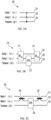
- FIG. 3A is a quantum circuit diagram 300 between a first cavity 301, a second cavity 302 and an ancilla transmon 303.
- the illustrated method for implementing the e-SWAP operation is as follows: (1) initialize the ancilla transmon 303 to the quantum state
- + ⁇ 1/ ⁇ 2(
- e ⁇ ); (2) perform a first c-SWAP operation 311 between the first cavity 301 and the second cavity 302 controlled based on the state of the ancilla transmon 303; (3) rotate 312 the ancilla transmon 303 by angle 2 ⁇ around the X axis X ⁇ e i ⁇ x ; and (4) perform a second c-SWAP operation 313 between the first cavity 301 and the second cavity 302 controlled based on the state of the ancilla transmon 303.
- the ancilla transmon is restored to the initial state
- FIG. 3B illustrates a quantum circuit diagram 320 for implementing the e-SWAP operation of FIG. 3A using BS operations and CPS operations.
- the c-SWAP gates are simply replaced with the c-SWAP method shown in FIG. 2B .
- the method of implementing the e-SWAP gate includes: (1) initializing the ancilla transmon 303 to the quantum state
- + ⁇ 1/ ⁇ 2(
- a simplified and more robust implementation of the e-SWAP operator can be obtained by decomposing the c-SWAP operators into beam splitter operators and CPS gates in a way that is different from simply substituting the quantum circuit diagram 210 of FIG. 2B into the quantum circuit diagram 300 of FIG. 3A .
- the simplification of the quantum circuit diagram 320 comes from the realization the two of the beam splitter operations are redundant (e.g., the second and third beam splitter operations 323 and 325) as they cancel each other and can therefore be removed.
- the transmon can be initialized in the ground state and additional Hadamard gates can be added to act on the transmon just before the first CPS gate 322 and after the second CPS gate 326, so that the transmon is kept in the ground state during the beam splitter unitary operations.
- the method of implementing the e-SWAP gate includes: (1) initializing the ancilla transmon 303 to the quantum state
Landscapes
- Engineering & Computer Science (AREA)
- Physics & Mathematics (AREA)
- Theoretical Computer Science (AREA)
- General Physics & Mathematics (AREA)
- Computing Systems (AREA)
- Mathematical Physics (AREA)
- General Engineering & Computer Science (AREA)
- Software Systems (AREA)
- Data Mining & Analysis (AREA)
- Mathematical Optimization (AREA)
- Pure & Applied Mathematics (AREA)
- Mathematical Analysis (AREA)
- Evolutionary Computation (AREA)
- Condensed Matter Physics & Semiconductors (AREA)
- Computational Mathematics (AREA)
- Artificial Intelligence (AREA)
- Computer Hardware Design (AREA)
- Optical Modulation, Optical Deflection, Nonlinear Optics, Optical Demodulation, Optical Logic Elements (AREA)
- Superconductor Devices And Manufacturing Methods Thereof (AREA)
- Logic Circuits (AREA)
- Semiconductor Lasers (AREA)
Claims (15)
- Ein Verfahren zum Implementieren eines Satzes von universellen Quantengattern, wobei der Satz von universellen Quantengattern ein gesteuertes-SWAP (c-SWAP)-Gatter und/oder ein exponentielles-SWAP (e-SWAP)-Gatter zwischen einer Vielzahl von Hohlräumen aufweist, aufweisend einen ersten Hohlraum (111) und einen zweiten Hohlraum (121), wobei ein erstes Qubit in dem ersten Hohlraum (111) kodiert wird und ein zweites Qubit in dem zweiten Hohlraum (121) kodiert wird, wobei das Verfahren Folgendes aufweist:Durchführen, durch Anlegen von Mikrowellenstrahlung an ein Kopplungstransmon (131), das dispersiv sowohl mit dem ersten Hohlraum (111) als auch mit dem zweiten Hohlraum (121) gekoppelt ist, einer ersten und einer zweiten Strahlteileroperation (BS) zwischen dem ersten Hohlraum (111) und dem zweiten Hohlraum (121);Durchführen, durch Anlegen von Mikrowellenstrahlung an ein Hilfstransmon (151), das dispersiv an den zweiten Hohlraum (121) gekoppelt ist, aber nicht an den ersten Hohlraum (111) gekoppelt ist, einer ersten und/oder einer zweiten kontrollierten Phasenverschiebungsoperation (CPS) zwischen dem zweiten Hohlraum (121) und dem Hilfstransmon (151); undDurchführen, durch Anlegen von Mikrowellenstrahlung an das Hilfstransmon (151), einer Rotationsoperation an dem Hilfstransmon (151).
- Das Verfahren nach Anspruch 1, wobei das Quantenlogik-Gatter ein c-SWAP-Gatter aufweist, wobei:die erste BS-Operation vor der ersten CPS-Operation durchgeführt wird und die zweite BS-Operation nach der ersten CPS-Operation durchgeführt wird,die erste BS-Operation mit einer Phase von θ=π/4 durchgeführt wird, unddie zweite BS-Operation mit einer Phase von θ=-π/4 durchgeführt wird.
- Das Verfahren nach Anspruch 2 oder einem anderen vorhergehenden Anspruch, wobei das Quantenlogik-Gatter ein e-SWAP-Gatter aufweist und das Verfahren Folgendes aufweist:Durchführen eines ersten c-SWAP-Gatters zwischen dem ersten Hohlraum (111) und dem zweiten Hohlraum (121);Durchführen eines zweiten c-SWAP-Gatters zwischen dem ersten Hohlraum (111) und dem zweiten Hohlraum (121); undDurchführen der Rotationsoperation an dem Hilfstransmon (151) zwischen dem ersten c-SWAP-Gate und dem zweiten c-SWAP-Gate.
- Das Verfahren nach Anspruch 2 oder einem anderen vorhergehenden Anspruch, wobei das Quantenlogik-Gatter ein e-SWAP-Gatter aufweist, und das Verfahren Folgendes aufweist:Durchführen der ersten CPS-Operation zwischen dem zweiten Hohlraum (121) und dem Hilfstransmon (151) nach der ersten BS-Operation;Durchführen der zweiten CPS-Operation zwischen dem zweiten Hohlraum (121) und dem Hilfstransmon (151) nach der ersten CPS-Operation und vor der zweiten BS-Operation; undDurchführen des Rotationsvorgangs an dem Hilfstransmon (151) zwischen dem ersten CPS-Vorgang und dem zweiten CPS-Vorgang.
- Das Verfahren nach Anspruch 4, das ferner Folgendes aufweist:Durchführen einer ersten Hadamard-Operation an dem Hilfstransmon (151) vor der ersten CPS-Operation und nach der ersten BS-Operation; undDurchführen einer zweiten Hadamard-Operation an dem Hilfstransmon (151) nach der zweiten CPS-Operation und vor der zweiten BS-Operation.
- Das Verfahren nach Anspruch 5, das ferner Folgendes aufweist:Initialisieren eines Zustands des Hilfstransmons (151) vor der Durchführung der ersten BS-Operation;Messen des Hilfstransmons (151) nach der Durchführung der zweiten BS-Operation; undBestimmen, dass ein Entphasungsfehler aufgetreten ist, basierend auf einem Ergebnis der Messung des Hilfstransmons (151).
- Das Verfahren nach Anspruch 6, wobei:wenigstens vier Energieniveaus des Hilfstransmons (151) verwendet werden;ein erstes Energieniveau des Hilfstransmons (151) einem ersten Zerfallsfehlertyp zugeordnet ist, der mit einem spontanen Zerfall eines Zustands des Hilfstransmons (151) verbunden ist, der während der ersten CPS-Operation auftritt;ein zweites Energieniveau des Hilfstransmons (151) mit einem zweiten Zerfallsfehlertyp verbunden ist, der mit einem spontanen Zerfall des Zustands des Hilfstransmons (151) verbunden ist, der während der zweiten CPS-Operation aufgetreten ist; unddas Verfahren ferner Korrigieren von Zerfallsfehlern aufweist, basierend auf einem Ergebnis der Messung des Hilfstransmons (151).
- Das Verfahren nach Anspruch 1, wobei:wenigstens ein lokales Quantenlogik-Gatter an dem Hilfstransmon (151) vor und/oder nach der ersten und/oder zweiten CPS-Operation durchgeführt wird,das wenigstens eine lokale Quantenlogikgatter eine erste Hadamard-Operation aufweist, die nach der ersten BS-Operation und vor der ersten CPS-Operation durchgeführt wird; unddas Verfahren ferner Messen des Zustands des Hilfstransmons (151) aufweist zum Vergleichen eines ersten Quantenzustands des ersten Hohlraums (111) mit einem zweiten Quantenzustand des zweiten Hohlraums (121).
- Das Verfahren nach Anspruch 2, wobei:die Vielzahl von Hohlräumen ferner einen dritten Hohlraum (Hohlraum 1') und einen vierten Hohlraum (Hohlraum 2') aufweist, wobei ein drittes Qubit in dem dritten Hohlraum und ein viertes Qubit in dem vierten Hohlraum kodiert wird;das Kopplungstransmon (131) ein erstes Kopplungstransmon ist;das Hilfstransmon (151) dispersiv mit dem dritten Hohlraum gekoppelt ist, aber nicht mit dem vierten Hohlraum gekoppelt ist; unddas Verfahren ferner Folgendes aufweist:Durchführen einer dritten BS-Operation zwischen dem dritten Hohlraum und dem vierten Hohlraum unter Verwendung eines zweiten Kopplungstransmon, das dispersiv sowohl mit dem dritten Hohlraum als auch mit dem vierten Hohlraum gekoppelt ist; undDurchführen der zweiten CPS-Operation zwischen dem dritten Hohlraum und dem Hilfstransmon (151).
- Das Verfahren nach Anspruch 9, wobei das Verfahren ferner Folgendes aufweist:Durchführen einer vierten BS-Operation zwischen dem dritten Hohlraum und dem vierten Hohlraum unter Verwendung des zweiten Kopplungstransmons, wobei die vierte BS-Operation vor der zweiten CPS-Operation durchgeführt wird und die zweite BS-Operation nach der zweiten CPS-Operation durchgeführt wird;Durchführen einer dritten CPS-Operation zwischen dem dritten Hohlraum und dem Hilfstransmon (151) nach der zweiten CPS-Operation und vor der vierten BS-Operation;Durchführen der Rotationsoperation an dem Hilfstransmon (151) zwischen der zweiten CPS-Operation und der dritten CPS-Operation;Durchführen einer vierten CPS-Operation zwischen dem zweiten Hohlraum (121) und dem Hilfstransmon (151) nach der dritten CPS-Operation und vor der zweiten BS-Operation;Durchführen einer ersten Hadamard-Operation an dem Hilfstransmon (151) vor der ersten CPS-Operation und nach der ersten und dritten BS-Operation; undDurchführen einer zweiten Hadamard-Operation an dem Hilfstransmon (151) nach der vierten CPS-Operation und vor der zweiten und vierten BS-Operation.
- Ein Quanteninformationssystem mit mehreren Hohlräumen, das Folgendes aufweist:einen ersten Hohlraum (111), der konfiguriert ist zum Unterstützen von Mikrowellenstrahlung;einen zweiten Hohlraum (121), der konfiguriert ist zum Unterstützen von Mikrowellenstrahlung;ein erstes Transmon (131), das dispersiv sowohl mit dem ersten Hohlraum (111) als auch mit dem zweiten Hohlraum (121) gekoppelt ist;ein zweites Transmon (151), das dispersiv mit dem zweiten Hohlraum (121), aber nicht mit dem ersten Hohlraum (111) gekoppelt ist; undeine Mikrowellenquelle (106), die konfiguriert ist zum, wenn ein erstes Qubit in dem ersten Hohlraum kodiert ist und ein zweites Qubit in dem zweiten Hohlraum kodiert ist:Anlegen von Mikrowellenstrahlung an das erste Transmon (131 zum Implementieren einer ersten und einer zweiten Strahlteileroperation (BS) zwischen dem ersten Hohlraum (111) und dem zweiten Hohlraum (121);Anlegen von Mikrowellenstrahlung an das zweite Transmon (151 zum Implementieren einer ersten und/oder einer zweiten kontrollierten Phasenverschiebungsoperation (CPS) zwischen dem zweiten Hohlraum (121) und dem zweiten Transmon (151); undAnlegen von Mikrowellenstrahlung an das zweite Transmon (151) zum Implementieren von Transmon-Rotationsoperationen an dem zweiten Transmon (151).
- Das Quanteninformationssystem mit mehreren Hohlräumen nach Anspruch 11, das ferner ein drittes Transmon (141) aufweist, das dispersiv mit dem ersten Hohlraum (111) gekoppelt ist, wobei die Mikrowellenquelle (106) ferner konfiguriert ist zum:Anlegen von Mikrowellenstrahlung an das dritte Transmon (141) zum Implementieren von Transmon-Rotationsoperationen an dem dritten Transmon (141); undAnlegen von Mikrowellenstrahlung an das dritte Transmon (141) zum Implementieren der ersten und/oder zweiten CPS-Operation zwischen dem ersten Hohlraum (111) und dem dritten Transmon (141); undAnlegen von Mikrowellenstrahlung an das erste, zweite und dritte Transmon (131, 151, 141) zum Implementieren eines Satzes von universellen Quantengattern zwischen dem ersten Hohlraum (111) und dem zweiten Hohlraum (121) durch Implementieren einer oder mehrerer BS-Operationen zwischen dem ersten Hohlraum (111) und dem zweiten Hohlraum (121), eine oder mehrere Transmon-Rotationsoperationen an dem zweiten Transmon (151) und/oder dem dritten Transmon (141) und/oder eine oder mehrere CPS-Operationen zwischen dem ersten Hohlraum (111) und dem dritten Transmon (141) und/oder zwischen dem zweiten Hohlraum (121) und dem zweiten Transmon (151).
- Das Quanteninformationssystem mit mehreren Hohlräumen nach Anspruch 12, wobei die Mikrowellenquelle (106) ferner konfiguriert ist zum Implementieren eines gesteuerten SWAP (c-SWAP)-Gatters zwischen dem ersten Hohlraum (111) und dem zweiten Hohlraum (121) durch:Anlegen von Mikrowellenstrahlung an das erste Transmon (131) zum Implementieren der ersten Strahlteileroperation (BS) zwischen dem ersten Hohlraum (111) und dem zweiten Hohlraum (121);Anlegen von Mikrowellenstrahlung an das zweite Transmon (151) oder das dritte Transmon (141) zum Implementieren der ersten kontrollierten Phasenverschiebungsoperation (CPS) zwischen dem ersten Hohlraum (111) und dem dritten Transmon (141) oder zwischen dem zweiten Hohlraum (121) und dem zweiten Transmon (151); undnach Durchführen der ersten CPS-Operation, Anlegen von Mikrowellenstrahlung an das erste Transmon (131) zum Implementieren der zweiten BS-Operation zwischen dem ersten Hohlraum (111) und dem zweiten Hohlraum (121), wobei:die erste BS-Operation mit einer Phase von θ=π/4 durchgeführt wird, unddie zweite BS-Operation mit einer Phase von θ=-π/4 durchgeführt wird.
- Das Quanteninformationssystem mit mehreren Hohlräumen nach Anspruch 13, wobei die Mikrowellenquelle (106) ferner konfiguriert ist zum Implementieren eines exponentiellen SWAP (e-SWAP) Gatters zwischen dem ersten Hohlraum (111) und dem zweiten Hohlraum (121) durch:Durchführen eines ersten c-SWAP-Gatters zwischen dem ersten Hohlraum (111) und dem zweiten Hohlraum (121);Durchführen eines zweiten c-SWAP-Gates zwischen dem ersten Hohlraum (111) und dem zweiten Hohlraum (121); undDurchführen der Transmon-Rotationsoperation an dem zweiten Transmon (151) zwischen dem ersten c-SWAP-Gate und dem zweiten c-SWAP-Gate.
- Das Quanteninformationssystem mit mehreren Hohlräumen nach Anspruch 12, wobei die Mikrowellenquelle (106) ferner konfiguriert ist zum:Anlegen von Mikrowellenstrahlung an das dritte und/oder zweite Transmon (141, 151) zum Ermöglichen von Messung des dritten und/oder zweiten Transmons (141, 151); undAnlegen von Mikrowellenstrahlung an das erste, zweite und/oder dritte Transmon (131, 151, 141) zum Implementieren eines Quantengatters basierend auf einem Ergebnis der Messung des dritten und/oder zweiten Transmon (141, 151).
Applications Claiming Priority (3)
| Application Number | Priority Date | Filing Date | Title |
|---|---|---|---|
| US201862613937P | 2018-01-05 | 2018-01-05 | |
| US201862733326P | 2018-09-19 | 2018-09-19 | |
| PCT/US2019/012440 WO2019156759A2 (en) | 2018-01-05 | 2019-01-05 | Robust quantum logical gates |
Publications (3)
| Publication Number | Publication Date |
|---|---|
| EP3735710A2 EP3735710A2 (de) | 2020-11-11 |
| EP3735710A4 EP3735710A4 (de) | 2021-09-15 |
| EP3735710B1 true EP3735710B1 (de) | 2024-11-20 |
Family
ID=67548387
Family Applications (1)
| Application Number | Title | Priority Date | Filing Date |
|---|---|---|---|
| EP19751562.0A Active EP3735710B1 (de) | 2018-01-05 | 2019-01-05 | Robuste quantenlogikgatter |
Country Status (8)
| Country | Link |
|---|---|
| US (1) | US11451231B2 (de) |
| EP (1) | EP3735710B1 (de) |
| JP (1) | JP7372681B2 (de) |
| KR (2) | KR102929433B1 (de) |
| CN (1) | CN111542935B (de) |
| CA (1) | CA3085954A1 (de) |
| SG (1) | SG11202005645RA (de) |
| WO (1) | WO2019156759A2 (de) |
Families Citing this family (13)
| Publication number | Priority date | Publication date | Assignee | Title |
|---|---|---|---|---|
| CN119940566A (zh) * | 2018-09-25 | 2025-05-06 | 谷歌有限责任公司 | 用于近似目标量子状态的方法和装置 |
| SG11202109186VA (en) * | 2019-03-01 | 2021-09-29 | Univ Yale | Techniques for quantum memory addressing and related systems and methods |
| CN114651263A (zh) * | 2019-09-13 | 2022-06-21 | 匹兹堡大学-属高等教育联邦体系 | 用于量子计算的参量驱动相干信号路由器及相关方法 |
| WO2021202409A1 (en) | 2020-03-30 | 2021-10-07 | Psiquantum, Corp. | Encoded fusion measurements with local adaptivity |
| CN112101561B (zh) * | 2020-08-24 | 2022-10-18 | 清华大学 | 一种实现量子逻辑门的方法及装置 |
| US11923870B2 (en) * | 2020-10-27 | 2024-03-05 | National Applied Research Laboratories | Method for constructing a fault tolerant encode using a quantum computational model |
| CN113012066B (zh) * | 2021-03-15 | 2022-06-17 | 中南大学 | 基于参数化玻色采样的量子线路学习方法及图像模糊方法 |
| JP2024513655A (ja) * | 2021-03-19 | 2024-03-27 | ノール クアンティキ インコーポレイテッド | 量子サブシステムのビット反転エラーのタイプと位相反転エラーのタイプとを同時に阻止するシステム、方法、及び制御命令 |
| US12198011B2 (en) | 2021-06-25 | 2025-01-14 | Korea Advanced Institute Of Science And Technology | Quantum computing device and method of mitigating detection crosstalk |
| KR20240126442A (ko) * | 2021-12-22 | 2024-08-20 | 예일 유니버시티 | 4-legged cat 코드를 위한 측정 기반 내결함성 아키텍처 |
| CN116562384B (zh) * | 2023-07-10 | 2023-09-12 | 合肥硅臻芯片技术有限公司 | 一种Fredkin量子逻辑门 |
| CN118348690B (zh) * | 2024-06-17 | 2024-08-30 | 合肥国家实验室 | 非耗散的虚时演化方法、干涉装置及量子冷却装置 |
| US20260087398A1 (en) * | 2024-09-26 | 2026-03-26 | Red Hat, Inc. | Quantum code space administration |
Family Cites Families (47)
| Publication number | Priority date | Publication date | Assignee | Title |
|---|---|---|---|---|
| US6578018B1 (en) | 1999-07-27 | 2003-06-10 | Yamaha Hatsudoki Kabushiki Kaisha | System and method for control using quantum soft computing |
| EP1262911A1 (de) | 2001-05-30 | 2002-12-04 | Hitachi Europe Limited | Quantenrechner |
| US6803599B2 (en) | 2001-06-01 | 2004-10-12 | D-Wave Systems, Inc. | Quantum processing system for a superconducting phase qubit |
| US20050240311A1 (en) | 2002-03-04 | 2005-10-27 | Herschel Rabitz | Closed-loop apparatuses for non linear system identification via optimal control |
| US7018852B2 (en) | 2002-08-01 | 2006-03-28 | D-Wave Systems, Inc. | Methods for single qubit gate teleportation |
| US6943368B2 (en) | 2002-11-25 | 2005-09-13 | D-Wave Systems, Inc. | Quantum logic using three energy levels |
| US7006267B2 (en) | 2002-12-09 | 2006-02-28 | The Johns Hopkins University | Techniques for high fidelity quantum teleportation and computing |
| US6989523B2 (en) | 2003-04-11 | 2006-01-24 | Hewlett-Packard Development Company, L.P. | Photon number resolving systems and methods |
| US7230266B2 (en) | 2003-05-15 | 2007-06-12 | D-Wave Systems Inc. | Conditional Rabi oscillation readout for quantum computing |
| US7133173B2 (en) * | 2004-07-26 | 2006-11-07 | Hewlett-Packard Development Company, L.P. | Nonlinear electromagnetic quantum information processing |
| US8983303B2 (en) | 2004-08-04 | 2015-03-17 | The United States Of America As Represented By The Secretary Of The Army | Quantum based information transfer system and method |
| US7359101B2 (en) | 2004-09-13 | 2008-04-15 | Hewleet-Packard Development Company, L.P. | Tests of quantum information |
| US20060067293A1 (en) | 2004-09-24 | 2006-03-30 | John Santhoff | Digital synthesis of communication signals |
| US7639947B2 (en) | 2005-09-19 | 2009-12-29 | The Chinese University Of Hong Kong | System and methods for quantum key distribution over WDM links |
| JP4599290B2 (ja) | 2005-12-27 | 2010-12-15 | 株式会社東芝 | 量子情報処理装置および方法 |
| MY153146A (en) | 2007-05-11 | 2014-12-31 | Mimos Berhad | Qudits in two way deterministic quantum key distribution |
| US7899092B2 (en) | 2007-05-22 | 2011-03-01 | Magiq Technologies, Inc. | Fast quantum gates with ultrafast chirped pulses |
| US7498832B2 (en) | 2007-08-03 | 2009-03-03 | Northrop Grumman Systems Corporation | Arbitrary quantum operations with a common coupled resonator |
| US8149494B1 (en) | 2007-09-07 | 2012-04-03 | The United States Of America As Represented By The Secretary Of The Navy | Two-photon absorption switch having which-path exclusion and monolithic mach-zehnder interferometer |
| BRPI0908763A2 (pt) | 2008-02-07 | 2015-07-28 | Lahav Gan | Dispositivo, método para a obtenção de uma referência de freqüência e sistema. |
| US7969178B2 (en) | 2008-05-29 | 2011-06-28 | Northrop Grumman Systems Corporation | Method and apparatus for controlling qubits with single flux quantum logic |
| JP5091813B2 (ja) | 2008-09-17 | 2012-12-05 | 株式会社東芝 | 量子ゲート方法および装置 |
| CN102210908A (zh) | 2010-04-09 | 2011-10-12 | 李连冬 | 一种多维次生物全息自律平衡系统 |
| US8242799B2 (en) | 2010-11-16 | 2012-08-14 | Northrop Grumman Systems Corporation | System and method for phase error reduction in quantum systems |
| US9379303B2 (en) * | 2011-06-14 | 2016-06-28 | Glocbalfoundries Inc. | Modular array of fixed-coupling quantum systems for quantum information processing |
| US8508280B2 (en) | 2011-07-11 | 2013-08-13 | Northrop Grumman Systems Corporation | Qubit readout via resonant scattering of josephson solitons |
| EP2581773A1 (de) | 2011-10-14 | 2013-04-17 | Astrium Limited | Vorrichtung mit Quantenschachtschicht |
| US8841764B2 (en) | 2012-01-31 | 2014-09-23 | International Business Machines Corporation | Superconducting quantum circuit having a resonant cavity thermalized with metal components |
| CN102593694B (zh) | 2012-02-15 | 2013-12-04 | 北京大学 | 基于四能级量子系统的主动激光频率标准 |
| US9787312B2 (en) | 2012-08-14 | 2017-10-10 | Northrop Grumman Systems Corporation | Systems and methods for applying flux to a quantum-coherent superconducting circuit |
| US8972921B2 (en) | 2013-03-14 | 2015-03-03 | International Business Machines Corporation | Symmetric placement of components on a chip to reduce crosstalk induced by chip modes |
| US9350460B2 (en) * | 2013-04-23 | 2016-05-24 | Raytheon Bbn Technologies Corp. | System and method for quantum information transfer between optical photons and superconductive qubits |
| CN105474027A (zh) | 2013-05-03 | 2016-04-06 | 量子谷投资基金有限合伙公司 | 转移自旋极化 |
| CA2927326C (en) | 2013-10-15 | 2024-02-27 | Yale University | Low-noise josephson junction-based directional amplifier |
| JP6576949B2 (ja) | 2014-01-06 | 2019-09-18 | グーグル エルエルシー | 量子アニーリング工程のための量子ハードウェアの構築およびプログラミング |
| GB201403063D0 (en) | 2014-02-21 | 2014-04-09 | Isis Innovation | Quantum technology |
| US10650319B2 (en) | 2015-02-06 | 2020-05-12 | Northrop Grumman Systems Corporation | Flux control of qubit under resonant excitation |
| JP2018513452A (ja) | 2015-02-27 | 2018-05-24 | イェール ユニバーシティーYale University | 量子コヒーレント状態のユニバーサル量子制御のための技術ならびに関連のある系および方法 |
| KR20170123657A (ko) | 2015-02-27 | 2017-11-08 | 예일 유니버시티 | 양자 정보 처리를 위한 발진기 제어 기술 그리고 관련 시스템 및 방법 |
| US9524470B1 (en) | 2015-06-12 | 2016-12-20 | International Business Machines Corporation | Modular array of vertically integrated superconducting qubit devices for scalable quantum computing |
| FR3038165B1 (fr) | 2015-06-29 | 2017-07-28 | Commissariat Energie Atomique | Procede de controle de la qualite d'un dispositif photovoltaique, et dispositif de controle associe |
| CA2993006C (en) | 2015-07-24 | 2023-10-03 | Yale University | Techniques of oscillator state manipulation for quantum information processing and related systems and methods |
| US9847121B2 (en) | 2015-09-13 | 2017-12-19 | International Business Machines Corporation | Providing controlled pulses for quantum computing |
| US9991864B2 (en) * | 2015-10-14 | 2018-06-05 | Microsoft Technology Licensing, Llc | Superconducting logic compatible phase shifter |
| CN108290733B (zh) * | 2015-12-04 | 2022-04-26 | 耶鲁大学 | 使用玻色子模式进行量子纠错的技术及相关系统和方法 |
| US10467544B2 (en) * | 2015-12-31 | 2019-11-05 | International Business Machines Corporation | Multi-qubit tunable coupling architecture using fixed-frequency superconducting qubits |
| US10776709B2 (en) | 2016-11-10 | 2020-09-15 | Yale University | Generalized quantum channels |
-
2019
- 2019-01-05 WO PCT/US2019/012440 patent/WO2019156759A2/en not_active Ceased
- 2019-01-05 CN CN201980007288.6A patent/CN111542935B/zh active Active
- 2019-01-05 EP EP19751562.0A patent/EP3735710B1/de active Active
- 2019-01-05 KR KR1020257013909A patent/KR102929433B1/ko active Active
- 2019-01-05 US US16/959,184 patent/US11451231B2/en active Active
- 2019-01-05 SG SG11202005645RA patent/SG11202005645RA/en unknown
- 2019-01-05 KR KR1020207021833A patent/KR20200104374A/ko not_active Ceased
- 2019-01-05 CA CA3085954A patent/CA3085954A1/en active Pending
- 2019-01-05 JP JP2020536949A patent/JP7372681B2/ja active Active
Also Published As
| Publication number | Publication date |
|---|---|
| CN111542935A (zh) | 2020-08-14 |
| KR20200104374A (ko) | 2020-09-03 |
| KR20250068771A (ko) | 2025-05-16 |
| WO2019156759A2 (en) | 2019-08-15 |
| CA3085954A1 (en) | 2019-08-15 |
| KR102929433B1 (ko) | 2026-02-20 |
| US11451231B2 (en) | 2022-09-20 |
| CN111542935B (zh) | 2024-01-26 |
| WO2019156759A3 (en) | 2019-09-26 |
| EP3735710A4 (de) | 2021-09-15 |
| EP3735710A2 (de) | 2020-11-11 |
| US20200412369A1 (en) | 2020-12-31 |
| SG11202005645RA (en) | 2020-07-29 |
| JP2021509771A (ja) | 2021-04-01 |
| JP7372681B2 (ja) | 2023-11-01 |
Similar Documents
| Publication | Publication Date | Title |
|---|---|---|
| US11451231B2 (en) | Robust quantum logical gates | |
| US12288135B2 (en) | Quantum information processing with an asymmetric error channel | |
| KR102632759B1 (ko) | 초전도 회로를 이용하는 하드웨어 효율적인 장애 허용 연산 | |
| Knill et al. | A scheme for efficient quantum computation with linear optics | |
| US20230376817A1 (en) | Systems and Methods for Deterministic Photonic Quantum Computing in a Synthetic Time Dimension | |
| Adami et al. | Quantum computation with linear optics | |
| KR20230018381A (ko) | N-큐비트 양자 게이트의 실행 | |
| Scarani | Quantum computing | |
| US20250356232A9 (en) | Measurement-based fault tolerant architecture for the 4-legged cat code | |
| HK40042690A (en) | Robust quantum logical gates | |
| HK40042690B (en) | Robust quantum logical gates | |
| Mikhail et al. | Comparative Study of Optical Quantum Swap Gates Using qINTERCONNECT | |
| Sheets et al. | Introduction to quantum computing | |
| JP2025540827A (ja) | キュービットのデュアルレールエンコーディングのための技術ならびに関連するシステムおよび方法 | |
| JP2025534337A (ja) | 論理キュービット上でもつれゲートを実行するための技術ならびに関連のあるシステムおよび方法 | |
| Wu et al. | Universal quantum computation using exchange interactions and teleportation of single-qubit operations | |
| Wang | An Universal Quantum Network-Quantum CPU | |
| García López | Optical quantum computation: information processing using discrete-and continuous-variable states of light | |
| Anning | QUANTUM COMPUTATION | |
| Ouellette | Quantum computation | |
| Yamaguchi et al. | Concurrent Quantum Computation | |
| Arvind | Implementing Logic Gates and the Deutsch–Jozsa Quantum Algorithm by Two-Dimensional NMR Using Spin-and Transition-Selective Pulses |
Legal Events
| Date | Code | Title | Description |
|---|---|---|---|
| STAA | Information on the status of an ep patent application or granted ep patent |
Free format text: STATUS: THE INTERNATIONAL PUBLICATION HAS BEEN MADE |
|
| PUAI | Public reference made under article 153(3) epc to a published international application that has entered the european phase |
Free format text: ORIGINAL CODE: 0009012 |
|
| STAA | Information on the status of an ep patent application or granted ep patent |
Free format text: STATUS: REQUEST FOR EXAMINATION WAS MADE |
|
| 17P | Request for examination filed |
Effective date: 20200630 |
|
| AK | Designated contracting states |
Kind code of ref document: A2 Designated state(s): AL AT BE BG CH CY CZ DE DK EE ES FI FR GB GR HR HU IE IS IT LI LT LU LV MC MK MT NL NO PL PT RO RS SE SI SK SM TR |
|
| AX | Request for extension of the european patent |
Extension state: BA ME |
|
| DAV | Request for validation of the european patent (deleted) | ||
| DAX | Request for extension of the european patent (deleted) | ||
| REG | Reference to a national code |
Ref country code: DE Ref legal event code: R079 Free format text: PREVIOUS MAIN CLASS: H01L0039220000 Ipc: G06N0010000000 Ref document number: 602019062243 Country of ref document: DE |
|
| REG | Reference to a national code |
Ref country code: HK Ref legal event code: DE Ref document number: 40042690 Country of ref document: HK |
|
| A4 | Supplementary search report drawn up and despatched |
Effective date: 20210817 |
|
| RIC1 | Information provided on ipc code assigned before grant |
Ipc: H01P 5/18 20060101ALI20210811BHEP Ipc: B82Y 10/00 20110101ALI20210811BHEP Ipc: H03K 19/195 20060101ALI20210811BHEP Ipc: G06N 99/00 20190101ALI20210811BHEP Ipc: H01L 39/22 20060101ALI20210811BHEP Ipc: G06N 10/00 20190101AFI20210811BHEP |
|
| STAA | Information on the status of an ep patent application or granted ep patent |
Free format text: STATUS: EXAMINATION IS IN PROGRESS |
|
| 17Q | First examination report despatched |
Effective date: 20230623 |
|
| REG | Reference to a national code |
Ref country code: DE Ref legal event code: R079 Free format text: PREVIOUS MAIN CLASS: G06N0010000000 Ipc: G06N0010200000 Ref document number: 602019062243 Country of ref document: DE |
|
| GRAP | Despatch of communication of intention to grant a patent |
Free format text: ORIGINAL CODE: EPIDOSNIGR1 |
|
| STAA | Information on the status of an ep patent application or granted ep patent |
Free format text: STATUS: GRANT OF PATENT IS INTENDED |
|
| RIC1 | Information provided on ipc code assigned before grant |
Ipc: B82Y 10/00 20110101ALI20240522BHEP Ipc: H01P 5/18 20060101ALI20240522BHEP Ipc: H03K 19/195 20060101ALI20240522BHEP Ipc: G06N 10/40 20220101ALI20240522BHEP Ipc: G06N 10/20 20220101AFI20240522BHEP |
|
| INTG | Intention to grant announced |
Effective date: 20240618 |
|
| GRAS | Grant fee paid |
Free format text: ORIGINAL CODE: EPIDOSNIGR3 |
|
| GRAA | (expected) grant |
Free format text: ORIGINAL CODE: 0009210 |
|
| STAA | Information on the status of an ep patent application or granted ep patent |
Free format text: STATUS: THE PATENT HAS BEEN GRANTED |
|
| AK | Designated contracting states |
Kind code of ref document: B1 Designated state(s): AL AT BE BG CH CY CZ DE DK EE ES FI FR GB GR HR HU IE IS IT LI LT LU LV MC MK MT NL NO PL PT RO RS SE SI SK SM TR |
|
| REG | Reference to a national code |
Ref country code: GB Ref legal event code: FG4D |
|
| P01 | Opt-out of the competence of the unified patent court (upc) registered |
Free format text: CASE NUMBER: APP_56776/2024 Effective date: 20241017 |
|
| REG | Reference to a national code |
Ref country code: CH Ref legal event code: EP |
|
| REG | Reference to a national code |
Ref country code: DE Ref legal event code: R096 Ref document number: 602019062243 Country of ref document: DE |
|
| REG | Reference to a national code |
Ref country code: IE Ref legal event code: FG4D |
|
| REG | Reference to a national code |
Ref country code: LT Ref legal event code: MG9D |
|
| REG | Reference to a national code |
Ref country code: NL Ref legal event code: MP Effective date: 20241120 |
|
| PG25 | Lapsed in a contracting state [announced via postgrant information from national office to epo] |
Ref country code: PT Free format text: LAPSE BECAUSE OF FAILURE TO SUBMIT A TRANSLATION OF THE DESCRIPTION OR TO PAY THE FEE WITHIN THE PRESCRIBED TIME-LIMIT Effective date: 20250320 Ref country code: HR Free format text: LAPSE BECAUSE OF FAILURE TO SUBMIT A TRANSLATION OF THE DESCRIPTION OR TO PAY THE FEE WITHIN THE PRESCRIBED TIME-LIMIT Effective date: 20241120 Ref country code: IS Free format text: LAPSE BECAUSE OF FAILURE TO SUBMIT A TRANSLATION OF THE DESCRIPTION OR TO PAY THE FEE WITHIN THE PRESCRIBED TIME-LIMIT Effective date: 20250320 |
|
| PG25 | Lapsed in a contracting state [announced via postgrant information from national office to epo] |
Ref country code: FI Free format text: LAPSE BECAUSE OF FAILURE TO SUBMIT A TRANSLATION OF THE DESCRIPTION OR TO PAY THE FEE WITHIN THE PRESCRIBED TIME-LIMIT Effective date: 20241120 Ref country code: NL Free format text: LAPSE BECAUSE OF FAILURE TO SUBMIT A TRANSLATION OF THE DESCRIPTION OR TO PAY THE FEE WITHIN THE PRESCRIBED TIME-LIMIT Effective date: 20241120 |
|
| REG | Reference to a national code |
Ref country code: AT Ref legal event code: MK05 Ref document number: 1744249 Country of ref document: AT Kind code of ref document: T Effective date: 20241120 |
|
| PG25 | Lapsed in a contracting state [announced via postgrant information from national office to epo] |
Ref country code: BG Free format text: LAPSE BECAUSE OF FAILURE TO SUBMIT A TRANSLATION OF THE DESCRIPTION OR TO PAY THE FEE WITHIN THE PRESCRIBED TIME-LIMIT Effective date: 20241120 |
|
| PG25 | Lapsed in a contracting state [announced via postgrant information from national office to epo] |
Ref country code: ES Free format text: LAPSE BECAUSE OF FAILURE TO SUBMIT A TRANSLATION OF THE DESCRIPTION OR TO PAY THE FEE WITHIN THE PRESCRIBED TIME-LIMIT Effective date: 20241120 |
|
| PG25 | Lapsed in a contracting state [announced via postgrant information from national office to epo] |
Ref country code: NO Free format text: LAPSE BECAUSE OF FAILURE TO SUBMIT A TRANSLATION OF THE DESCRIPTION OR TO PAY THE FEE WITHIN THE PRESCRIBED TIME-LIMIT Effective date: 20250220 |
|
| PG25 | Lapsed in a contracting state [announced via postgrant information from national office to epo] |
Ref country code: GR Free format text: LAPSE BECAUSE OF FAILURE TO SUBMIT A TRANSLATION OF THE DESCRIPTION OR TO PAY THE FEE WITHIN THE PRESCRIBED TIME-LIMIT Effective date: 20250221 Ref country code: AT Free format text: LAPSE BECAUSE OF FAILURE TO SUBMIT A TRANSLATION OF THE DESCRIPTION OR TO PAY THE FEE WITHIN THE PRESCRIBED TIME-LIMIT Effective date: 20241120 Ref country code: LV Free format text: LAPSE BECAUSE OF FAILURE TO SUBMIT A TRANSLATION OF THE DESCRIPTION OR TO PAY THE FEE WITHIN THE PRESCRIBED TIME-LIMIT Effective date: 20241120 |
|
| PG25 | Lapsed in a contracting state [announced via postgrant information from national office to epo] |
Ref country code: PL Free format text: LAPSE BECAUSE OF FAILURE TO SUBMIT A TRANSLATION OF THE DESCRIPTION OR TO PAY THE FEE WITHIN THE PRESCRIBED TIME-LIMIT Effective date: 20241120 |
|
| PG25 | Lapsed in a contracting state [announced via postgrant information from national office to epo] |
Ref country code: RS Free format text: LAPSE BECAUSE OF FAILURE TO SUBMIT A TRANSLATION OF THE DESCRIPTION OR TO PAY THE FEE WITHIN THE PRESCRIBED TIME-LIMIT Effective date: 20250220 |
|
| PG25 | Lapsed in a contracting state [announced via postgrant information from national office to epo] |
Ref country code: SM Free format text: LAPSE BECAUSE OF FAILURE TO SUBMIT A TRANSLATION OF THE DESCRIPTION OR TO PAY THE FEE WITHIN THE PRESCRIBED TIME-LIMIT Effective date: 20241120 |
|
| PG25 | Lapsed in a contracting state [announced via postgrant information from national office to epo] |
Ref country code: DK Free format text: LAPSE BECAUSE OF FAILURE TO SUBMIT A TRANSLATION OF THE DESCRIPTION OR TO PAY THE FEE WITHIN THE PRESCRIBED TIME-LIMIT Effective date: 20241120 |
|
| PG25 | Lapsed in a contracting state [announced via postgrant information from national office to epo] |
Ref country code: EE Free format text: LAPSE BECAUSE OF FAILURE TO SUBMIT A TRANSLATION OF THE DESCRIPTION OR TO PAY THE FEE WITHIN THE PRESCRIBED TIME-LIMIT Effective date: 20241120 |
|
| PG25 | Lapsed in a contracting state [announced via postgrant information from national office to epo] |
Ref country code: RO Free format text: LAPSE BECAUSE OF FAILURE TO SUBMIT A TRANSLATION OF THE DESCRIPTION OR TO PAY THE FEE WITHIN THE PRESCRIBED TIME-LIMIT Effective date: 20241120 |
|
| PG25 | Lapsed in a contracting state [announced via postgrant information from national office to epo] |
Ref country code: SK Free format text: LAPSE BECAUSE OF FAILURE TO SUBMIT A TRANSLATION OF THE DESCRIPTION OR TO PAY THE FEE WITHIN THE PRESCRIBED TIME-LIMIT Effective date: 20241120 |
|
| PG25 | Lapsed in a contracting state [announced via postgrant information from national office to epo] |
Ref country code: CZ Free format text: LAPSE BECAUSE OF FAILURE TO SUBMIT A TRANSLATION OF THE DESCRIPTION OR TO PAY THE FEE WITHIN THE PRESCRIBED TIME-LIMIT Effective date: 20241120 |
|
| REG | Reference to a national code |
Ref country code: DE Ref legal event code: R097 Ref document number: 602019062243 Country of ref document: DE |
|
| REG | Reference to a national code |
Ref country code: CH Ref legal event code: PL |
|
| PG25 | Lapsed in a contracting state [announced via postgrant information from national office to epo] |
Ref country code: SE Free format text: LAPSE BECAUSE OF FAILURE TO SUBMIT A TRANSLATION OF THE DESCRIPTION OR TO PAY THE FEE WITHIN THE PRESCRIBED TIME-LIMIT Effective date: 20241120 |
|
| PG25 | Lapsed in a contracting state [announced via postgrant information from national office to epo] |
Ref country code: LU Free format text: LAPSE BECAUSE OF NON-PAYMENT OF DUE FEES Effective date: 20250105 Ref country code: MC Free format text: LAPSE BECAUSE OF FAILURE TO SUBMIT A TRANSLATION OF THE DESCRIPTION OR TO PAY THE FEE WITHIN THE PRESCRIBED TIME-LIMIT Effective date: 20241120 |
|
| PLBE | No opposition filed within time limit |
Free format text: ORIGINAL CODE: 0009261 |
|
| STAA | Information on the status of an ep patent application or granted ep patent |
Free format text: STATUS: NO OPPOSITION FILED WITHIN TIME LIMIT |
|
| PG25 | Lapsed in a contracting state [announced via postgrant information from national office to epo] |
Ref country code: BE Free format text: LAPSE BECAUSE OF NON-PAYMENT OF DUE FEES Effective date: 20250131 |
|
| PG25 | Lapsed in a contracting state [announced via postgrant information from national office to epo] |
Ref country code: CH Free format text: LAPSE BECAUSE OF NON-PAYMENT OF DUE FEES Effective date: 20250131 |
|
| 26N | No opposition filed |
Effective date: 20250821 |
|
| REG | Reference to a national code |
Ref country code: BE Ref legal event code: MM Effective date: 20250131 |
|
| PG25 | Lapsed in a contracting state [announced via postgrant information from national office to epo] |
Ref country code: IE Free format text: LAPSE BECAUSE OF NON-PAYMENT OF DUE FEES Effective date: 20250105 |
|
| PGFP | Annual fee paid to national office [announced via postgrant information from national office to epo] |
Ref country code: GB Payment date: 20260127 Year of fee payment: 8 |
|
| PGFP | Annual fee paid to national office [announced via postgrant information from national office to epo] |
Ref country code: DE Payment date: 20260128 Year of fee payment: 8 |
|
| PGFP | Annual fee paid to national office [announced via postgrant information from national office to epo] |
Ref country code: IT Payment date: 20260121 Year of fee payment: 8 |
|
| PGFP | Annual fee paid to national office [announced via postgrant information from national office to epo] |
Ref country code: FR Payment date: 20260126 Year of fee payment: 8 |