EP3736840B1 - Ensemble inducteur et haut-parleur - Google Patents
Ensemble inducteur et haut-parleur Download PDFInfo
- Publication number
- EP3736840B1 EP3736840B1 EP19743230.5A EP19743230A EP3736840B1 EP 3736840 B1 EP3736840 B1 EP 3736840B1 EP 19743230 A EP19743230 A EP 19743230A EP 3736840 B1 EP3736840 B1 EP 3736840B1
- Authority
- EP
- European Patent Office
- Prior art keywords
- coil
- inductor
- wound
- magnetic circuit
- diode
- Prior art date
- Legal status (The legal status is an assumption and is not a legal conclusion. Google has not performed a legal analysis and makes no representation as to the accuracy of the status listed.)
- Active
Links
Images

Classifications
-
- H—ELECTRICITY
- H01—ELECTRIC ELEMENTS
- H01F—MAGNETS; INDUCTANCES; TRANSFORMERS; SELECTION OF MATERIALS FOR THEIR MAGNETIC PROPERTIES
- H01F21/00—Variable inductances or transformers of the signal type
- H01F21/02—Variable inductances or transformers of the signal type continuously variable, e.g. variometers
-
- H—ELECTRICITY
- H01—ELECTRIC ELEMENTS
- H01F—MAGNETS; INDUCTANCES; TRANSFORMERS; SELECTION OF MATERIALS FOR THEIR MAGNETIC PROPERTIES
- H01F27/00—Details of transformers or inductances, in general
- H01F27/40—Structural association with built-in electric component, e.g. fuse
-
- H—ELECTRICITY
- H01—ELECTRIC ELEMENTS
- H01F—MAGNETS; INDUCTANCES; TRANSFORMERS; SELECTION OF MATERIALS FOR THEIR MAGNETIC PROPERTIES
- H01F21/00—Variable inductances or transformers of the signal type
- H01F21/12—Variable inductances or transformers of the signal type discontinuously variable, e.g. tapped
-
- H—ELECTRICITY
- H01—ELECTRIC ELEMENTS
- H01F—MAGNETS; INDUCTANCES; TRANSFORMERS; SELECTION OF MATERIALS FOR THEIR MAGNETIC PROPERTIES
- H01F27/00—Details of transformers or inductances, in general
- H01F27/28—Coils; Windings; Conductive connections
-
- H—ELECTRICITY
- H01—ELECTRIC ELEMENTS
- H01F—MAGNETS; INDUCTANCES; TRANSFORMERS; SELECTION OF MATERIALS FOR THEIR MAGNETIC PROPERTIES
- H01F27/00—Details of transformers or inductances, in general
- H01F27/28—Coils; Windings; Conductive connections
- H01F27/2823—Wires
-
- H—ELECTRICITY
- H01—ELECTRIC ELEMENTS
- H01F—MAGNETS; INDUCTANCES; TRANSFORMERS; SELECTION OF MATERIALS FOR THEIR MAGNETIC PROPERTIES
- H01F27/00—Details of transformers or inductances, in general
- H01F27/42—Circuits specially adapted for the purpose of modifying, or compensating for, electric characteristics of transformers, reactors, or choke coils
Definitions
- the present disclosure relates to the field of electrical devices, and more particularly, relates to an inductor assembly and a speaker.
- An inductor is an element configured to convert electrical energy into magnetic energy and store the magnetic energy, which is an important part of the power system.
- problems such as voltage fluctuations and harmonic pollution may be caused.
- the inductance of the inductor shall be adjusted during the operation.
- the inductor includes a core, a first coil and a second coil which are wound on the core.
- the first coil is configured to be connected to an operating circuit (the current in the operating circuit is an alternating current), which enables the second coil to generate an induced current.
- the inductance of the inductor needs to be adjusted, it is necessary to apply direct current to the second coil, and constantly change a magnitude of the direct current, so as to change a saturation degree of the core, then change a magnitude of the inductance of the first coil, and adjust an inductance of the inductor.
- JP2004140165A describes a variable inductor comprising: a first inductor having a prescribed inductance value, a second inductor having a prescribed inductance value which is formed to possess a mutual inductance with the first inductor, and a variable resistor connected across terminals of the second inductor. A resistance value of the variable resistor is continuously changed. Thus, the inductance value between terminals and of the first inductor can be changed.
- CN1790565A describes a non-contact controllable reactor, which separates the dc control winding and ac operating winding in space, uses the adjustable hollow solenoid, the hollow solenoid with variable dc excitation, and the semi-iron core/circular-iron core straight solenoid with dc excitation as control winding.
- regulating the reactance value by changing magnetic flux, controlling the magnetic saturation degree of semi-iron core, and controlling the rotation direction of magnetic domain of circular-iron core in cross magnetic field improving the nonlinear character of traditional product, reducing harmonic wave quantity and reactor volume.
- RU2348998C1 describes a reactor provided with a closed core, its central rod being within the closed core, control winding coiled on the central rod, network winding and control unit.
- the cylindrical rod is available in the reactor. It is situated concentrically with regard to the central rod and linked with the closed core.
- CN202309082U describes an automatic stepless voltage regulating type reactive power compensator, which includes a capacitor set and a control portion thereof, wherein the line of the capacitor set connected to the electric network is serially connected with an adjustable reactor; the adjustable reactor comprises a primary side coil serially connected between the capacitor set and the electric network; the adjustable reactor is provided with a secondary control coil, with a bidirectional thyristor being connected between two ends of the secondary control coil; the control electrode of the bidirectional thyristor is connected with the intelligent controller; a detecting apparatus of the electric network reactive current is arranged upon the line of the capacitor set connected to the electric network; and the output of the detecting apparatus of the electric network reactive current is connected with the intelligent controller.
- Embodiments of the present invention provide an inductor assembly and a speaker, which may solve the above-mentioned technical problems.
- the technical solutions are as follows:
- inventions of the present invention provide an inductor assembly.
- the inductor assembly includes an inductor and a current regulating device;
- the first coil and the second coil are both air-core coils.
- the inductor further includes a magnetic circuit core; wherein the first coil and the second coil are both wound on the magnetic circuit core.
- the magnetic circuit core includes a closed magnetic circuit core;
- the closed magnetic circuit core is one of a ring-shaped core and a ring-shaped core with a slit on a side wall.
- the magnetic circuit core includes an open magnetic circuit core; wherein
- the open magnetic circuit core is a rod-shaped core.
- inventions of the present invention provide a speaker.
- the speaker includes a frequency divider; wherein the frequency divider includes the above-mentioned inductor assembly.
- a first coil, a second coil, and a current regulating device are provided, and two ends of the second coil are connected to the current regulating device in series by means of conducting wires. After the first coil is connected to an operating circuit, the second coil is enabled to generate an induced current.
- An inductor is an element configured to convert electrical energy into magnetic energy and store the the magnetic energy, and is widely used in life. When the inductor is used, it is often necessary to adjust the inductance of the inductor.
- the saturation inductance method is configured for adjustment.
- the inductor used in this method includes a core, a first coil and a second coil which are wound on the core. During the adjustment process, apply direct current to the second coil, and constantly change the magnitude of the direct current, so as to change the saturation degree of the core, and then change the magnitude of the inductance of the first coil. This method will cause current flowing through the inductor to be distorted or generate harmonics.
- the induced current generated by the second coil is configured to change a magnitude of a reverse magnetic flux by changing a magnitude of the current flowing through the second coil, so as to realize linear adjustment of the inductance of the inductor.
- the adjustment process is simple, and the air-core inductor, the open magnetic circuit inductor, and the closed-loop magnetic circuit inductor may all be linearly adjusted, which not only responds quickly, but also does not distort a waveform of the current flowing through the first coil.
- the closed-loop magnetic circuit inductor includes a first coil, a second coil and a closed magnetic circuit core.
- I 1 N 1 I 2 N 2
- the magnetic flux of the closed magnetic circuit core is zero.
- I 1 is the current in the first coil
- N 1 is the number of turns of the first coil
- I 2 is the current in the second coil
- N 2 is the number of turns of the second coil.
- an embodiment of the present disclosure provides an inductor assembly.
- the inductor includes an inductor and a current regulating device 5.
- the inductor includes a first coil 1 and a second coil 2, wherein the first coil 1 is configured to, after being connected to an operating circuit, enable the second coil 2 to generate an induced current; two ends of the second coil 2 are connected to the current regulating device 5 in series by means of conducting wires, and the current regulating device 5 is configured to regulate the magnitude of the induced current generated by the second coil 2.
- the first coil 1 is connected to the operating circuit (it may be understood that the current applied at this moment to the first coil 1 is an alternating current), which enables the second coil 2 to generate an induced current.
- the current regulating device 5 is configured to regulate a magnitude of current in the second coil 2, and then a magnitude of a magnetic flux of the second coil 2 is changed. At this moment, an inductance of the inductor in the inductor assembly is regulated.
- the "operating circuit” refers to the circuit where a load is disposed.
- a first coil 1, a second coil 2, and a current regulating device 5 are provided, and two ends of the second coil 2 are connected to the current regulating device 5 in series by means of conducting wires. After the first coil 1 is connected to an operating circuit, the second coil 2 is enabled to generate an induced current.
- the inductance of the inductor in the inductor assembly needs to be changed, only the current regulating device 5 needs to be regulated, and the operations are simple.
- inductors with various structures are all applicable to the inductor assembly according to the embodiment of the present disclosure, and the following is optional:
- both the first coil 1 and the second coil 2 may be arranged as air-core coils, and the second coil 2 is wound on the first coil 1.
- the first coil 1 is wound on the second coil 2.
- the first coil 1 and the second coil 2 are co-wound.
- the inductor assembly may be applied to occasions with a wide range of frequencies, ensuring that most audio frequencies may pass through smoothly.
- the term "co-wound” refers to that the first coil 1 and the second coil 2 are mixed and co-wound to form a layer of air-core coils (in each of the above-mentioned situation in which the second coil 2 is wound on the first coil 1, or the first coil 1 is wound on the second coil 2, the first coil 1 and the second coil 2 form two layers of air-core coils).
- two wires are placed side by side for winding.
- FIG. 1 it may be seen that in the above-mentioned layer of air-core coils, the wires belonging to the first coil 1 are arranged alternately with the wires belonging to the second coil 2.
- the inductor assembly further includes a magnetic circuit core.
- the first coil 1 and the second coil 2 are both wound on the magnetic circuit core.
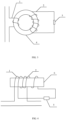
- the magnetic circuit core includes a closed magnetic circuit core 4, and the first coil 1 and the second coil 2 are both wound on the closed magnetic circuit core 4, for example, as shown in FIG. 2 .
- the winding methods of the first coil 1 and the second coil 2 mentioned above may be as follows: the first coil 1 is wound on the closed magnetic core 4, and the second coil 2 is wound on the first coil 1; or the second coil 2 is wound on the closed magnetic circuit core 4, and the first coil 1 is wound on the second coil 2; or the first coil 1 and the second coil 2 are co-wound on the closed magnetic circuit core 4.
- the embodiment of the present disclosure does not limit the winding method of the first coil 1 and the second coil 2.
- the first coil 1 and the second coil 2 may be wound respectively at different positions on the closed magnetic circuit core 4.
- the first coil 1 is connected to the operating circuit to enable the second coil 2 to generate the induced current.
- the current regulating device 5 is configured to regulate the magnitude of the current in the second coil 2, and then the magnitude of the magnetic flux of the closed magnetic circuit core 4 is changed. At this moment, the inductance of the inductor in the inductor assembly is regulated.
- the closed magnetic circuit core 4 may be in various structures.
- the closed magnetic circuit core may be a ring structure, or a double-C-shaped structure with notches butted against each other, or a ring structure with a slit on the side wall, or the like.
- the inductor assembly further includes an open magnetic circuit core 6.
- the first coil 1 is wound on the open magnetic circuit core 6, and the second coil 2 is wound on the first coil 1.
- the second coil 2 is wound on the open magnetic circuit core 6, and the first coil 1 is wound on the second coil 2.
- the first coil 1 and the second coil 2 are co-wound on the open magnetic circuit core 6.
- the first coil 1 is connected to the operating circuit to enable the second coil 2 to generate the induced current.
- the current regulating device 5 is configured to regulate the magnitude of the current in the second coil 2, and then the magnitude of the magnetic flux of the open magnetic circuit core 6 is changed. At this moment, the inductance of the inductor in the inductor assembly is regulated.
- the embodiment of the present disclosure does not limit the structure of the open magnetic circuit core 6.
- the open magnetic circuit core 6 may be a rod-shaped structure.
- the current regulating device 5 includes a variable resistor 3.
- the current regulating device includes a rectifier switching device.
- the variable resistor 3 and the rectifier switching device are described respectively:
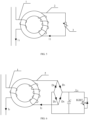
- the variable resistor 3 is a resistor whose resistance may be adjusted. As shown in FIG. 5 , the second coil 2 may be connected in series to the variable resistor 3 through wires (or another optional connection method), then the total resistance of the circuit where the second coil 2 is disposed is equal to the sum of the resistance of the second coil 2 and that of the variable resistor 3.
- the resistance value of the variable resistor 3 is adjusted, so as to change the total resistance of the circuit where the second coil 2 is disposed, thereby changing the current of the circuit where the second coil 2 is disposed.
- the magnetic flux of the second coil 2 is changed, and the inductance of the first coil 1 is changed accordingly. At this moment, the inductance of the inductor is regulated.
- the rectifier switching device is an insulated gate bipolar transistor.
- the insulated gate bipolar transistor (IGBT): it is a semiconductor element with a switching function.
- the application circuit of the IGBT is shown in FIG. 6 in which D1, D2, D3, D4, and D5 all represent diodes, C represents a capacitor, and L 1 represents an inductor.
- the IGBT and D5 are connected in parallel, and the IGBT and D5 in parallel are configured as a first element, then the first element and the inductor L 1 are connected in series to form a first sub-circuit.
- the first sub-circuit is connected in parallel to the capacitor C to form a branch circuit.
- two ends of the second coil 2 are connected in series to the branch circuit by D 2 and D 3 when the direction of the current I 2 in the second coil 2 is the direction shown in FIG. 6 . Accordingly, when the direction of the current I 2 in the second coil 2 is opposite to the direction shown in FIG. 6 , two ends of the second coil 2 are connected in series to the branch circuit through D 1 and D 4 . It can be seen that the second coil 2 is always connected in series to the branch circuit, that is, the circuit where the second coil 2 is disposed is always a closed circuit.
- the switching state of the IGBT may be changed by a computer.
- the value of the current in the circuit where the second coil 2 is disposed decreases; when the IGBT is switched from the off state to the on state, the value of the current in the second coil 2 is increased. Therefore, by regulating the switching frequencies of the IGBT by a computer, the switching states of the IGBT may be switched regularly, and the value of the current in the circuit where the second coil 2 is disposed will be changed accordingly, thus the effective value of I 2 is changed, and the current of the circuit where the second coil 2 is disposed may be adjusted. Therefore, the magnetic flux of the second coil 2 is changed, and the inductance of the first coil 1 is changed accordingly. At this moment, the inductance of the inductor is regulated.
- the function of the capacitor C is that when the switching state of the IGBT is changed, the capacitor may enable the current in the circuit where the second coil 2 is disposed to change, thereby preventing the current waveform of the circuit where the second coil 2 is disposed form being changed.
- the functions of the inductor L 1 are to prevent the generation of a surge current and protect the IGBT.
- a peak current which is a surge current
- the induced current generated by the second coil 2 is configured as a steady-state current, and the value of the surge current is greater than that of the steady-state current.
- L 1 is configured to prevent the generation of the surge current to protect the IGBT
- the rectifier switching device may include a thyristor or a triode.
- the thyristor is also a semiconductor element with a switching function.
- the principle of regulating the inductance of inductor by a thyristor is the same as that by an IGBT, which is not repeated herein.
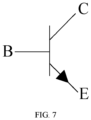
- the Triode the schematic diagram of the triode is shown in FIG. 7 in which B, C and E are the three electrodes of the triode respectively.
- the current from C to E is expressed as Ic
- the current from B to E is expressed as Ib
- the value of Ic changes as the value of Ib changes. Therefore, the two electrodes C and E may be connected to the two ends of the second coil 2 respectively, and then the current in the circuit where the second coil 2 is disposed is Ic.
- Ic is indirectly controlled by controlling Ib such that the magnetic flux of the second coil 2 is changed, and the inductance of the first coil 1 is also changed accordingly. At this moment, the inductance of the inductor is regulated.
- the embodiment of the present disclosure provides a speaker which includes a frequency divider.
- the frequency divider includes the above-mentioned inductor assembly.
- the speaker also has the above advantages of the inductor assembly.
- a user may regulate the inductance according to his or her own preference, such that the frequency divider may better divide the frequencies of the speaker and make the response frequencies of the speaker become wider.
- the structure of the speaker is common in the art, and it is also common in the art to provide a frequency divider and an inductor assembly in the speaker.
- a reference may be made to patents such as the application No. CN00240314 . 5 entitled HIGH-FIDELITY SPEAKER.
Landscapes
- Engineering & Computer Science (AREA)
- Power Engineering (AREA)
- Coils Or Transformers For Communication (AREA)
- Amplifiers (AREA)
Claims (8)
- Un ensemble inducteur, dans lequelL'ensemble inducteur comprend : un inducteur et un régulateur de courant (5) ; dans lequelL'inducteur comprend : une première bobine (1) et une deuxième bobine (2) ; dans lequella deuxième bobine (2) est configurée pour générer un courant induit lorsqu'un courant alternatif circule dans la première bobine (1) ; etdeux extrémités de la seconde bobine (2) sont connectées en série au régulateur de courant (5) par un fil conducteur, et le régulateur de courant (5) comprend un transistor bipolaire à grille isolée ;caractérisés en ce que le régulateur de courant (5) comprend en outre une première diode D1, une deuxième diode D2, une troisième diode D3, une quatrième diode D4, un condensateur C, une inductance L1, et une cinquième diode D5,dans lequel :une extrémité de la deuxième bobine (2) est connectée à une cathode de la première diode D1, et à une anode de la troisième diode D3, une autre extrémité de la deuxième bobine (2) est connectée à une cathode de la deuxième diode D2, et à une anode de la quatrième diode D4,l'anode de la première diode D1, est respectivement connectée à une anode de la deuxième diode D2, à une plaque du condensateur C, à une source du transistor bipolaire à grille isolée IGBT, et à l'anode de la cinquième diode D5,une cathode de la troisième diode D3, est respectivement connectée à une cathode de la quatrième diode D4, à une autre plaque du condensateur C, et à une extrémité de l'inducteur L1,une autre extrémité de l'inducteur L1, est respectivement connectée à un drain de transistor bipolaire à porte isolée IGBT, et à une cathode de la cinquième diode D5.
- L'ensemble inducteur selon la revendication 1, dans lequella première bobine (1) et la deuxième bobine (2) sont toutes deux des bobines à noyau d'air ; etla deuxième bobine (2) est enroulé sur la première bobine (1) ; oula première bobine (1) est enroulé sur la deuxième bobine (2) ; oula première bobine (1) et la deuxième bobine (2) enroulées ensemble.
- L'ensemble inducteur selon la revendication 1, dans lequel l'ensemble inducteur comprend en outre un noyau de circuit magnétique ;
dans lequel la première bobine (1) et la deuxième bobine (2) sont toutes deux enroulées sur le noyau du circuit magnétique. - L'ensemble inducteur selon la revendication 3, dans lequel le noyau du circuit magnétique comprend un coeur de circuit magnétique fermé (4) ; dans lequella première bobine (1) est enroulée sur le noyau du circuit magnétique fermé (4), et la deuxième bobine (2) est enroulée sur la première bobine (1) ; oula deuxième bobine (2) est enroulée sur le noyau du circuit magnétique fermé (4), et est enroulée sur la deuxième bobine (2) ; oualternativement, la première bobine (1) et la deuxième bobine (2) sont enroulées ensemble sur le noyau du circuit magnétique fermé (4).
- L'ensemble inducteur selon la revendication 4, dans lequel le noyau du circuit magnétique fermé (4) est un noyau en forme d'anneau et un noyau en forme d'anneau avec une fente sur une paroi latérale.
- L'ensemble inducteur selon la revendication 3, dans lequel le noyau du circuit magnétique comprend : un noyau de circuit magnétique ouvert (6) ; dans lequella première bobine (1) est enroulée sur le noyau du circuit magnétique ouvert (6), et la deuxième bobine (2) est enroulée sur la première bobine (1) ; oula deuxième bobine (2) est enroulée sur le noyau du circuit magnétique ouvert (6), et la première bobine (1) est enroulée sur la deuxième bobine (2) ; oula première bobine (1) et la deuxième bobine (2) sont enroulées ensemble sur le noyauc du circuit magnétique ouvert (6).
- L'ensemble inducteur selon la revendication 6, dans lequel le noyau du circuit magnétique ouvert (6) est un noyau en forme de bâtonnet.
- Le haut-parleur comprenant un diviseur de fréquence, dans lequel le diviseur de fréquence comprend l'ensemble inducteur tel que défini dans l'une des revendications 1 à 7.
Applications Claiming Priority (2)
| Application Number | Priority Date | Filing Date | Title |
|---|---|---|---|
| CN201810067576.8A CN108447665A (zh) | 2018-01-24 | 2018-01-24 | 一种可调电感器组件及音箱 |
| PCT/CN2019/072866 WO2019144887A1 (fr) | 2018-01-24 | 2019-01-23 | Ensemble inducteur et haut-parleur |
Publications (4)
| Publication Number | Publication Date |
|---|---|
| EP3736840A1 EP3736840A1 (fr) | 2020-11-11 |
| EP3736840A4 EP3736840A4 (fr) | 2021-03-10 |
| EP3736840C0 EP3736840C0 (fr) | 2023-08-23 |
| EP3736840B1 true EP3736840B1 (fr) | 2023-08-23 |
Family
ID=63191298
Family Applications (1)
| Application Number | Title | Priority Date | Filing Date |
|---|---|---|---|
| EP19743230.5A Active EP3736840B1 (fr) | 2018-01-24 | 2019-01-23 | Ensemble inducteur et haut-parleur |
Country Status (3)
| Country | Link |
|---|---|
| EP (1) | EP3736840B1 (fr) |
| CN (2) | CN108447665A (fr) |
| WO (1) | WO2019144887A1 (fr) |
Families Citing this family (5)
| Publication number | Priority date | Publication date | Assignee | Title |
|---|---|---|---|---|
| CN108447665A (zh) * | 2018-01-24 | 2018-08-24 | 北京金科华业测控技术有限公司 | 一种可调电感器组件及音箱 |
| CN110379611A (zh) * | 2019-06-26 | 2019-10-25 | 东南大学 | 一种具有永磁偏置的直流电流控制电感调谐装置 |
| CN110957659B (zh) * | 2019-11-20 | 2020-12-01 | 苏州鱼得水电气科技有限公司 | 一种移动式变电站 |
| CN118098791A (zh) * | 2022-11-28 | 2024-05-28 | 王静然 | 电感器及扬声器组件 |
| CN119786227B (zh) * | 2025-03-07 | 2025-05-09 | 深圳市海瑞思自动化科技有限公司 | 一种质谱用射频线圈电感量调节装置 |
Family Cites Families (16)
| Publication number | Priority date | Publication date | Assignee | Title |
|---|---|---|---|---|
| US4207530A (en) * | 1977-09-12 | 1980-06-10 | Motorola, Inc. | Electrically tunable inductor and method |
| JPH05182837A (ja) * | 1992-01-07 | 1993-07-23 | Matsushita Electric Ind Co Ltd | 可変インダクタ |
| US20040012472A1 (en) * | 1997-11-28 | 2004-01-22 | Christian Sasse | Flux control for high power static electromagnetic devices |
| CN2455028Y (zh) * | 2000-11-29 | 2001-10-17 | 梁耀辉 | 一种高保真音箱 |
| JP2004140165A (ja) * | 2002-10-17 | 2004-05-13 | Matsushita Electric Ind Co Ltd | 可変インダクタ |
| CN100483575C (zh) * | 2005-12-23 | 2009-04-29 | 清华大学 | 非接触式可控电抗器 |
| RU2348998C1 (ru) * | 2008-01-31 | 2009-03-10 | Александр Васильевич Григорьев | Управляемый реактор трансформаторного типа |
| CN201319287Y (zh) * | 2008-12-03 | 2009-09-30 | 上海铁路通信工厂 | 大电流空心线圈 |
| US20110260819A1 (en) * | 2010-04-26 | 2011-10-27 | Taiwan Semiconductor Manufacturing Co., Ltd. | Continuously tunable inductor with variable resistors |
| CN202309082U (zh) * | 2011-09-28 | 2012-07-04 | 武汉伏特克电气工程有限公司 | 自动无级调压式无功补偿装置 |
| CN102682955B (zh) * | 2012-05-10 | 2016-09-14 | 杭州金果科技有限公司 | 一种可调电感 |
| CN202759249U (zh) * | 2012-08-23 | 2013-02-27 | 大连第二互感器集团有限公司 | 磁控并联电抗器 |
| CN203311972U (zh) * | 2013-07-11 | 2013-11-27 | 哈尔滨理工大学 | 一种带气隙直流控磁可调电抗器 |
| CN204992589U (zh) * | 2015-10-10 | 2016-01-20 | 张家港市博特圣电气科技有限公司 | 一种三相交流智能控制电路 |
| CN107509134A (zh) * | 2017-10-10 | 2017-12-22 | 李龙根 | 一种耳机用二阶无源分频器 |
| CN108447665A (zh) * | 2018-01-24 | 2018-08-24 | 北京金科华业测控技术有限公司 | 一种可调电感器组件及音箱 |
-
2018
- 2018-01-24 CN CN201810067576.8A patent/CN108447665A/zh active Pending
-
2019
- 2019-01-23 WO PCT/CN2019/072866 patent/WO2019144887A1/fr not_active Ceased
- 2019-01-23 CN CN201980021874.6A patent/CN111954913A/zh active Pending
- 2019-01-23 EP EP19743230.5A patent/EP3736840B1/fr active Active
Also Published As
| Publication number | Publication date |
|---|---|
| EP3736840C0 (fr) | 2023-08-23 |
| WO2019144887A1 (fr) | 2019-08-01 |
| CN111954913A (zh) | 2020-11-17 |
| EP3736840A1 (fr) | 2020-11-11 |
| CN108447665A (zh) | 2018-08-24 |
| EP3736840A4 (fr) | 2021-03-10 |
Similar Documents
| Publication | Publication Date | Title |
|---|---|---|
| EP3736840A1 (fr) | Ensemble inducteur et haut-parleur | |
| US5942884A (en) | Electronic transformer/regulator | |
| US10992217B2 (en) | Insulated power source and power conversion device | |
| WO2010027742A2 (fr) | Régulation de tension et correction du facteur de puissance dans les moteurs à induction alternatifs | |
| US8169756B2 (en) | Fault current limiting | |
| DE19702042A1 (de) | Spannungswandelnde Schaltungsanordnung zur Energieversorgung eines elektrischen Verbrauchers hoher Leistung, insbesondere einer Spulmaschine | |
| CN110914934B (zh) | 具有可变电感器的谐振变流器 | |
| KR101925182B1 (ko) | 변류기 기반의 유도형 전원공급 장치 | |
| US20200153354A1 (en) | Controlling voltage in ac power lines | |
| EP3841602B1 (fr) | Dispositif de regulation de courant | |
| KR101617857B1 (ko) | 전력 손실 감소 장치 | |
| CN201364801Y (zh) | 磁通抵消式电抗器 | |
| US5319534A (en) | Series-parallel active power line conditioner utilizing reduced-turns-ratio transformer for enhanced peak voltage regulation capability | |
| US20120314728A1 (en) | System and method to deliver and control power to an arc furnace | |
| US20100067274A1 (en) | Method and device for creating a direct voltage or a direct current | |
| JP2020141555A (ja) | Acネットワークにおける無効分損失を補償するための自動デバイス及び方法 | |
| US9343996B2 (en) | Method and system for transmitting voltage and current between a source and a load | |
| US4896091A (en) | Electric power converter | |
| CN115811238A (zh) | 交流电子变压器或调压器 | |
| CN119446716A (zh) | 一种用于交直流配电网的柔性配电变压器及安装设备 | |
| CN104485824A (zh) | 一种磁控孤立的多功能变压器 | |
| CN102158104A (zh) | 一种电压与电流调节器 | |
| RU2065654C1 (ru) | Управляемый реактор | |
| JP3582721B2 (ja) | Dc−dcコンバータ | |
| RU2554712C1 (ru) | Стабилизатор - регулятор напряжения переменного тока |
Legal Events
| Date | Code | Title | Description |
|---|---|---|---|
| STAA | Information on the status of an ep patent application or granted ep patent |
Free format text: STATUS: THE INTERNATIONAL PUBLICATION HAS BEEN MADE |
|
| PUAI | Public reference made under article 153(3) epc to a published international application that has entered the european phase |
Free format text: ORIGINAL CODE: 0009012 |
|
| STAA | Information on the status of an ep patent application or granted ep patent |
Free format text: STATUS: REQUEST FOR EXAMINATION WAS MADE |
|
| 17P | Request for examination filed |
Effective date: 20200804 |
|
| AK | Designated contracting states |
Kind code of ref document: A1 Designated state(s): AL AT BE BG CH CY CZ DE DK EE ES FI FR GB GR HR HU IE IS IT LI LT LU LV MC MK MT NL NO PL PT RO RS SE SI SK SM TR |
|
| AX | Request for extension of the european patent |
Extension state: BA ME |
|
| A4 | Supplementary search report drawn up and despatched |
Effective date: 20210209 |
|
| RIC1 | Information provided on ipc code assigned before grant |
Ipc: H01F 27/42 20060101ALI20210203BHEP Ipc: H01F 27/28 20060101ALI20210203BHEP Ipc: H01F 21/02 20060101ALI20210203BHEP Ipc: H01F 27/40 20060101AFI20210203BHEP Ipc: H01F 21/12 20060101ALI20210203BHEP |
|
| DAV | Request for validation of the european patent (deleted) | ||
| DAX | Request for extension of the european patent (deleted) | ||
| RIC1 | Information provided on ipc code assigned before grant |
Ipc: H01F 21/02 20060101ALI20230119BHEP Ipc: H01F 27/42 20060101ALI20230119BHEP Ipc: H01F 21/12 20060101ALI20230119BHEP Ipc: H01F 27/28 20060101ALI20230119BHEP Ipc: H01F 27/40 20060101AFI20230119BHEP |
|
| GRAP | Despatch of communication of intention to grant a patent |
Free format text: ORIGINAL CODE: EPIDOSNIGR1 |
|
| STAA | Information on the status of an ep patent application or granted ep patent |
Free format text: STATUS: GRANT OF PATENT IS INTENDED |
|
| INTG | Intention to grant announced |
Effective date: 20230307 |
|
| GRAS | Grant fee paid |
Free format text: ORIGINAL CODE: EPIDOSNIGR3 |
|
| GRAA | (expected) grant |
Free format text: ORIGINAL CODE: 0009210 |
|
| STAA | Information on the status of an ep patent application or granted ep patent |
Free format text: STATUS: THE PATENT HAS BEEN GRANTED |
|
| AK | Designated contracting states |
Kind code of ref document: B1 Designated state(s): AL AT BE BG CH CY CZ DE DK EE ES FI FR GB GR HR HU IE IS IT LI LT LU LV MC MK MT NL NO PL PT RO RS SE SI SK SM TR |
|
| REG | Reference to a national code |
Ref country code: GB Ref legal event code: FG4D |
|
| REG | Reference to a national code |
Ref country code: CH Ref legal event code: EP |
|
| REG | Reference to a national code |
Ref country code: DE Ref legal event code: R096 Ref document number: 602019035615 Country of ref document: DE |
|
| REG | Reference to a national code |
Ref country code: IE Ref legal event code: FG4D |
|
| U01 | Request for unitary effect filed |
Effective date: 20230823 |
|
| U07 | Unitary effect registered |
Designated state(s): AT BE BG DE DK EE FI FR IT LT LU LV MT NL PT SE SI Effective date: 20230901 |
|
| U1N | Appointed representative for the unitary patent procedure changed after the registration of the unitary effect |
Representative=s name: CHUNG, HOI KAN; GB |
|
| U20 | Renewal fee for the european patent with unitary effect paid |
Year of fee payment: 6 Effective date: 20231205 |
|
| PG25 | Lapsed in a contracting state [announced via postgrant information from national office to epo] |
Ref country code: GR Free format text: LAPSE BECAUSE OF FAILURE TO SUBMIT A TRANSLATION OF THE DESCRIPTION OR TO PAY THE FEE WITHIN THE PRESCRIBED TIME-LIMIT Effective date: 20231124 |
|
| PGFP | Annual fee paid to national office [announced via postgrant information from national office to epo] |
Ref country code: GB Payment date: 20231122 Year of fee payment: 6 |
|
| PG25 | Lapsed in a contracting state [announced via postgrant information from national office to epo] |
Ref country code: IS Free format text: LAPSE BECAUSE OF FAILURE TO SUBMIT A TRANSLATION OF THE DESCRIPTION OR TO PAY THE FEE WITHIN THE PRESCRIBED TIME-LIMIT Effective date: 20231223 |
|
| PG25 | Lapsed in a contracting state [announced via postgrant information from national office to epo] |
Ref country code: RS Free format text: LAPSE BECAUSE OF FAILURE TO SUBMIT A TRANSLATION OF THE DESCRIPTION OR TO PAY THE FEE WITHIN THE PRESCRIBED TIME-LIMIT Effective date: 20230823 Ref country code: NO Free format text: LAPSE BECAUSE OF FAILURE TO SUBMIT A TRANSLATION OF THE DESCRIPTION OR TO PAY THE FEE WITHIN THE PRESCRIBED TIME-LIMIT Effective date: 20231123 Ref country code: IS Free format text: LAPSE BECAUSE OF FAILURE TO SUBMIT A TRANSLATION OF THE DESCRIPTION OR TO PAY THE FEE WITHIN THE PRESCRIBED TIME-LIMIT Effective date: 20231223 Ref country code: HR Free format text: LAPSE BECAUSE OF FAILURE TO SUBMIT A TRANSLATION OF THE DESCRIPTION OR TO PAY THE FEE WITHIN THE PRESCRIBED TIME-LIMIT Effective date: 20230823 Ref country code: GR Free format text: LAPSE BECAUSE OF FAILURE TO SUBMIT A TRANSLATION OF THE DESCRIPTION OR TO PAY THE FEE WITHIN THE PRESCRIBED TIME-LIMIT Effective date: 20231124 |
|
| PG25 | Lapsed in a contracting state [announced via postgrant information from national office to epo] |
Ref country code: PL Free format text: LAPSE BECAUSE OF FAILURE TO SUBMIT A TRANSLATION OF THE DESCRIPTION OR TO PAY THE FEE WITHIN THE PRESCRIBED TIME-LIMIT Effective date: 20230823 |
|
| PG25 | Lapsed in a contracting state [announced via postgrant information from national office to epo] |
Ref country code: ES Free format text: LAPSE BECAUSE OF FAILURE TO SUBMIT A TRANSLATION OF THE DESCRIPTION OR TO PAY THE FEE WITHIN THE PRESCRIBED TIME-LIMIT Effective date: 20230823 |
|
| PG25 | Lapsed in a contracting state [announced via postgrant information from national office to epo] |
Ref country code: SM Free format text: LAPSE BECAUSE OF FAILURE TO SUBMIT A TRANSLATION OF THE DESCRIPTION OR TO PAY THE FEE WITHIN THE PRESCRIBED TIME-LIMIT Effective date: 20230823 Ref country code: RO Free format text: LAPSE BECAUSE OF FAILURE TO SUBMIT A TRANSLATION OF THE DESCRIPTION OR TO PAY THE FEE WITHIN THE PRESCRIBED TIME-LIMIT Effective date: 20230823 Ref country code: ES Free format text: LAPSE BECAUSE OF FAILURE TO SUBMIT A TRANSLATION OF THE DESCRIPTION OR TO PAY THE FEE WITHIN THE PRESCRIBED TIME-LIMIT Effective date: 20230823 Ref country code: CZ Free format text: LAPSE BECAUSE OF FAILURE TO SUBMIT A TRANSLATION OF THE DESCRIPTION OR TO PAY THE FEE WITHIN THE PRESCRIBED TIME-LIMIT Effective date: 20230823 Ref country code: SK Free format text: LAPSE BECAUSE OF FAILURE TO SUBMIT A TRANSLATION OF THE DESCRIPTION OR TO PAY THE FEE WITHIN THE PRESCRIBED TIME-LIMIT Effective date: 20230823 |
|
| REG | Reference to a national code |
Ref country code: DE Ref legal event code: R097 Ref document number: 602019035615 Country of ref document: DE |
|
| PLBE | No opposition filed within time limit |
Free format text: ORIGINAL CODE: 0009261 |
|
| STAA | Information on the status of an ep patent application or granted ep patent |
Free format text: STATUS: NO OPPOSITION FILED WITHIN TIME LIMIT |
|
| 26N | No opposition filed |
Effective date: 20240524 |
|
| PG25 | Lapsed in a contracting state [announced via postgrant information from national office to epo] |
Ref country code: MC Free format text: LAPSE BECAUSE OF FAILURE TO SUBMIT A TRANSLATION OF THE DESCRIPTION OR TO PAY THE FEE WITHIN THE PRESCRIBED TIME-LIMIT Effective date: 20230823 |
|
| PG25 | Lapsed in a contracting state [announced via postgrant information from national office to epo] |
Ref country code: MC Free format text: LAPSE BECAUSE OF FAILURE TO SUBMIT A TRANSLATION OF THE DESCRIPTION OR TO PAY THE FEE WITHIN THE PRESCRIBED TIME-LIMIT Effective date: 20230823 |
|
| REG | Reference to a national code |
Ref country code: CH Ref legal event code: PL |
|
| PG25 | Lapsed in a contracting state [announced via postgrant information from national office to epo] |
Ref country code: CH Free format text: LAPSE BECAUSE OF NON-PAYMENT OF DUE FEES Effective date: 20240131 |
|
| PG25 | Lapsed in a contracting state [announced via postgrant information from national office to epo] |
Ref country code: CH Free format text: LAPSE BECAUSE OF NON-PAYMENT OF DUE FEES Effective date: 20240131 |
|
| PG25 | Lapsed in a contracting state [announced via postgrant information from national office to epo] |
Ref country code: IE Free format text: LAPSE BECAUSE OF NON-PAYMENT OF DUE FEES Effective date: 20240123 |
|
| PG25 | Lapsed in a contracting state [announced via postgrant information from national office to epo] |
Ref country code: IE Free format text: LAPSE BECAUSE OF NON-PAYMENT OF DUE FEES Effective date: 20240123 |
|
| PG25 | Lapsed in a contracting state [announced via postgrant information from national office to epo] |
Ref country code: CY Free format text: LAPSE BECAUSE OF FAILURE TO SUBMIT A TRANSLATION OF THE DESCRIPTION OR TO PAY THE FEE WITHIN THE PRESCRIBED TIME-LIMIT; INVALID AB INITIO Effective date: 20190123 |
|
| PG25 | Lapsed in a contracting state [announced via postgrant information from national office to epo] |
Ref country code: HU Free format text: LAPSE BECAUSE OF FAILURE TO SUBMIT A TRANSLATION OF THE DESCRIPTION OR TO PAY THE FEE WITHIN THE PRESCRIBED TIME-LIMIT; INVALID AB INITIO Effective date: 20190123 |
|
| U90 | Renewal fees not paid: noting of loss of rights |
Free format text: RENEWAL FEE NOT PAID FOR YEAR 07 Effective date: 20250819 |
|
| GBPC | Gb: european patent ceased through non-payment of renewal fee |
Effective date: 20250123 |
|
| PG25 | Lapsed in a contracting state [announced via postgrant information from national office to epo] |
Ref country code: GB Free format text: LAPSE BECAUSE OF NON-PAYMENT OF DUE FEES Effective date: 20250123 |
|
| U93 | Unitary patent lapsed |
Free format text: RENEWAL FEE NOT PAID Effective date: 20250131 |
|
| PG25 | Lapsed in a contracting state [announced via postgrant information from national office to epo] |
Ref country code: TR Free format text: LAPSE BECAUSE OF FAILURE TO SUBMIT A TRANSLATION OF THE DESCRIPTION OR TO PAY THE FEE WITHIN THE PRESCRIBED TIME-LIMIT Effective date: 20230823 |