EP3740834B1 - Appareil et methode pour réduire au minimum une chute de tension causée par un courant de surcharge à l'entrée d'un régulateur de tension lors de l'allumage du régulateur de tension - Google Patents
Appareil et methode pour réduire au minimum une chute de tension causée par un courant de surcharge à l'entrée d'un régulateur de tension lors de l'allumage du régulateur de tension Download PDFInfo
- Publication number
- EP3740834B1 EP3740834B1 EP18830081.8A EP18830081A EP3740834B1 EP 3740834 B1 EP3740834 B1 EP 3740834B1 EP 18830081 A EP18830081 A EP 18830081A EP 3740834 B1 EP3740834 B1 EP 3740834B1
- Authority
- EP
- European Patent Office
- Prior art keywords
- voltage
- current
- resistance
- turn
- amount
- Prior art date
- Legal status (The legal status is an assumption and is not a legal conclusion. Google has not performed a legal analysis and makes no representation as to the accuracy of the status listed.)
- Active
Links
Images

Classifications
-
- H—ELECTRICITY
- H02—GENERATION; CONVERSION OR DISTRIBUTION OF ELECTRIC POWER
- H02H—EMERGENCY PROTECTIVE CIRCUIT ARRANGEMENTS
- H02H9/00—Emergency protective circuit arrangements for limiting excess current or voltage without disconnection
- H02H9/02—Emergency protective circuit arrangements for limiting excess current or voltage without disconnection responsive to excess current
-
- G—PHYSICS
- G05—CONTROLLING; REGULATING
- G05F—SYSTEMS FOR REGULATING ELECTRIC OR MAGNETIC VARIABLES
- G05F1/00—Automatic systems in which deviations of an electric quantity from one or more predetermined values are detected at the output of the system and fed back to a device within the system to restore the detected quantity to its predetermined value or values, i.e. retroactive systems
- G05F1/10—Regulating voltage or current
- G05F1/46—Regulating voltage or current wherein the variable actually regulated by the final control device is DC
-
- G—PHYSICS
- G05—CONTROLLING; REGULATING
- G05F—SYSTEMS FOR REGULATING ELECTRIC OR MAGNETIC VARIABLES
- G05F1/00—Automatic systems in which deviations of an electric quantity from one or more predetermined values are detected at the output of the system and fed back to a device within the system to restore the detected quantity to its predetermined value or values, i.e. retroactive systems
- G05F1/10—Regulating voltage or current
- G05F1/46—Regulating voltage or current wherein the variable actually regulated by the final control device is DC
- G05F1/468—Regulating voltage or current wherein the variable actually regulated by the final control device is DC characterised by reference voltage circuitry, e.g. soft start, remote shutdown
-
- G—PHYSICS
- G05—CONTROLLING; REGULATING
- G05F—SYSTEMS FOR REGULATING ELECTRIC OR MAGNETIC VARIABLES
- G05F1/00—Automatic systems in which deviations of an electric quantity from one or more predetermined values are detected at the output of the system and fed back to a device within the system to restore the detected quantity to its predetermined value or values, i.e. retroactive systems
- G05F1/10—Regulating voltage or current
- G05F1/46—Regulating voltage or current wherein the variable actually regulated by the final control device is DC
- G05F1/56—Regulating voltage or current wherein the variable actually regulated by the final control device is DC using semiconductor devices in series with the load as final control devices
- G05F1/565—Regulating voltage or current wherein the variable actually regulated by the final control device is DC using semiconductor devices in series with the load as final control devices sensing a condition of the system or its load in addition to means responsive to deviations in the output of the system, e.g. current, voltage, power factor
- G05F1/569—Regulating voltage or current wherein the variable actually regulated by the final control device is DC using semiconductor devices in series with the load as final control devices sensing a condition of the system or its load in addition to means responsive to deviations in the output of the system, e.g. current, voltage, power factor for protection
- G05F1/573—Regulating voltage or current wherein the variable actually regulated by the final control device is DC using semiconductor devices in series with the load as final control devices sensing a condition of the system or its load in addition to means responsive to deviations in the output of the system, e.g. current, voltage, power factor for protection with overcurrent detector
-
- G—PHYSICS
- G06—COMPUTING OR CALCULATING; COUNTING
- G06F—ELECTRIC DIGITAL DATA PROCESSING
- G06F1/00—Details not covered by groups G06F3/00 - G06F13/00 and G06F21/00
- G06F1/26—Power supply means, e.g. regulation thereof
-
- H—ELECTRICITY
- H02—GENERATION; CONVERSION OR DISTRIBUTION OF ELECTRIC POWER
- H02H—EMERGENCY PROTECTIVE CIRCUIT ARRANGEMENTS
- H02H9/00—Emergency protective circuit arrangements for limiting excess current or voltage without disconnection
- H02H9/001—Emergency protective circuit arrangements for limiting excess current or voltage without disconnection limiting speed of change of electric quantities, e.g. soft switching on or off
-
- H—ELECTRICITY
- H02—GENERATION; CONVERSION OR DISTRIBUTION OF ELECTRIC POWER
- H02M—APPARATUS FOR CONVERSION BETWEEN AC AND AC, BETWEEN AC AND DC, OR BETWEEN DC AND DC, AND FOR USE WITH MAINS OR SIMILAR POWER SUPPLY SYSTEMS; CONVERSION OF DC OR AC INPUT POWER INTO SURGE OUTPUT POWER; CONTROL OR REGULATION THEREOF
- H02M1/00—Details of apparatus for conversion
- H02M1/36—Means for starting or stopping converters
-
- H—ELECTRICITY
- H02—GENERATION; CONVERSION OR DISTRIBUTION OF ELECTRIC POWER
- H02M—APPARATUS FOR CONVERSION BETWEEN AC AND AC, BETWEEN AC AND DC, OR BETWEEN DC AND DC, AND FOR USE WITH MAINS OR SIMILAR POWER SUPPLY SYSTEMS; CONVERSION OF DC OR AC INPUT POWER INTO SURGE OUTPUT POWER; CONTROL OR REGULATION THEREOF
- H02M1/00—Details of apparatus for conversion
- H02M1/32—Means for protecting converters other than automatic disconnection
Definitions
- This invention relates to direct current (DC)voltage regulation and an initial surge of current, typically with an associated drop in voltage, at the input of the voltage regulator upon the voltage regulator being turned from OFF to ON.
- DC direct current
- the magnitude of such a current surge and associated voltage drop is greater when multiple voltage regulators are connected in parallel to the same power source and are switched from OFF to ON at substantially the same time.
- voltage regulator circuits In order to enhance output voltage stability, voltage regulator circuits often utilize a capacitor connected at the regulated output voltage terminal to ground that functions as a low pass filter to inhibit rapid voltage fluctuations at the regulated output voltage. While this is beneficial, as this output capacitor is normally in a discharged state, i.e. zero voltage across the capacitor, when the voltage regulator circuit is OFF. Depending on the resistance in series with the capacitor, large currents can initially flow upon turn-ON of the voltage regulator until the output capacitor becomes charged. Even if such a capacitor is not utilized as part of the voltage regulator circuit, the load circuit that receives the regulated voltage output from the voltage regulator circuit may have an input capacitor or equivalent capacitance that can give rise to such a current surge.
- the voltage at the supply voltage source (input to the voltage regulator) will drop. If it drops to a voltage level approaching the target regulated voltage output of one of the voltage regulators being supplied by the voltage source, then the output voltage of that voltage regulator will fall below the target voltage during such a current spike. This is undesirable and may cause errors or malfunctions by the load circuitry fed from the voltage regulator.
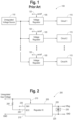
- FIG. 1 shows an embodiment 100 of voltage supply system with a plurality of voltage regulators 105 connected in parallel to an unregulated voltage source 110, e.g. a battery, etc.
- an unregulated voltage source 110 e.g. a battery, etc.
- Each of the voltage regulators 105 are connected to a corresponding load circuit 115.
- the voltage regulators 105 have a control terminal 120 by which the voltage regulators 105 are turned OFF and ON by a control voltage. If it is possible to sequence to the turning ON the respective voltage regulators 105, then any concurrent current surge and associated voltage drop induced at the unregulated voltage source can be minimized. However, the demands of the load circuits 115 may make such sequencing undesirable.
- a voltage regulator manufactured by ST Microelectronics, model RHFL4913A, is documented in a datasheet entitled " Rad-hard Adjustable Positive Voltage Regulator” that describes features and characteristics of this integrated circuit regulator and application information. It describes a PNP device controlled by a signal resulting from an amplified comparison between an internal temperature-compensated bandgap cell and a fraction of a desires output voltage value. The fractional value is obtained by an internal-to-die resistor divider bridge set at the factory. The device has current limit and thermal protection circuits.
- FIG. 2 shows a block diagram of a simplified voltage regulator 200. Only those aspects and parameters associated with the voltage regulator 200 that are useful in understanding the improvement in accordance with embodiments of the present invention are described in the interests of clarity and simplification.
- a voltage regulator integrated circuit (IC) 205 contains circuitry which provides for an adjustable regulated output voltage with a maximum current load of a few amperes. Some voltage regulator ICs have additional characteristics depending upon the particular application, e.g. such as being radiation hardened for use in high radiation environments. One such rad-hardened adjustable voltage regulator is the RHFL 4913A available from ST Microelectronics.
- the voltage regulator IC 205 includes a terminal 210 for receiving unregulated DC voltage from a DC voltage supply and a reference ground terminal 215.
- An output terminal 220 provides a regulated DC voltage output relative to ground terminal 225. It will be apparent to those skilled in the art that the unregulated DC voltage from the DC voltage supply should be higher than the selected target voltage appearing at terminal 220. For example, if a target regulated DC voltage of 3.75 V is desired, then an appropriate value for the unregulated input DC voltage could be 5.0 V or higher.
- Element 230 connected between the output regulated voltage terminal 220 and corresponding ground 225 represents a capacitor or an equivalent capacitance utilized to provide a low-pass filter action for the regulated DC voltage.
- An initiate (or inhibit) terminal 235 enables the DC regulator IC to be turned OFF and ON such as by a TTL control voltage.
- a short circuit current (SCC) terminal 240 provides an input to which one resistor 245 is suggested to be connected to the unregulated input voltage source to provide a fixed over current limitation, e.g. a limit on how much current can flow regardless of the current demand of a circuit connected to its output or even if the output 220 is short circuited to ground 225.
- SCC short circuit current
- the invention provides an apparatus that provides a regulated DC voltage output from an input supply DC voltage source, as set out in claim 1 appended hereto.
- the invention provides a method for controlling an initial voltage drop due to a turn-ON current surge at the input of a DC voltage regulator, as set out in claim 8 appended hereto.
- An exemplary apparatus provides a regulated DC voltage output from an input supply DC voltage source.
- a regulation circuit having an input terminal coupled to the supply DC voltage source, an output terminal on which is provided the regulated DC voltage output, and a current control terminal capable of controlling a maximum current that can flow through the regulation circuit where a level of maximum current is controlled proportionate to an amount of resistance connected to the current control terminal.
- a surge control circuit connected to the current control terminal automatically supplies a variable resistance beginning with one resistance at turn-ON and varying to another resistance at a predetermined time interval after turn-ON to limit the current that can flow at turn-ON until a steady state of the regulation circuit is reached.
- An exemplary method controls an initial voltage drop due to a turn-ON current surge at the input of a DC voltage regulator that provides a regulated DC voltage output from an input supply DC voltage source.
- a variable effective resistance is supplied to a current control terminal of a regulation circuit that is part of the DC voltage regulator upon the start of the initial turn-ON.
- the amount of resistance provided by the variable resistance corresponds to predetermined associated maximum currents that are permitted to flow through the regulation circuit, with the level of permitted maximum current being proportionate to the amount of resistance.
- the rate of change of the variable effective resistance is controlled based on a resistance-capacitance (RC) time constant established by a first resistor and a first capacitor coupled to the current control terminal.
- RC resistance-capacitance
- the variable effective resistance changes from a first amount of resistance at the turn-ON to a second amount of resistance at a predetermined time following the turn-ON.
- the first amount of resistance restricting the level of maximum current that can flow through the regulation circuit at the turn-ON to a first current level that is less than a second current level that corresponds to the second amount of resistance.
- the maximum current that can be drawn by the DC voltage regulator is controlled to a level that minimizes any voltage drop at the DC voltage source upon turn-ON.
- FIG. 3 shows a graph 300 of current versus resistance that allows a designer to select a resistance value for resistor 245 that sets a short circuit current value for the exemplary voltage regulator integrated circuit 205.
- the current in amperes is shown on the vertical axis 305 and corresponding values of resistance shown in 1000's of ohms (k ohms) are shown on the horizontal axis 310.
- the graph 315 shows that the corresponding maximum allowed short circuit current values are nonlinear. It will be understood that this specific short circuit current limitation versus resistance characteristic is dependent upon the particular design of the voltage regulator IC.
- FIG. 4 shows an exemplary circuit 400 in accordance with the present invention that can be utilized in conjunction with the exemplary voltage regulator IC 205 to control the initial turn-ON current surge while also providing a different level of steady state over current limit, where steady state means during normal ON operation following the initial OFF to ON startup condition.
- the circuit 400 includes resistors R1 and R2 connected in series between the unregulated voltage supply and the SCC terminal 240 of the voltage regulator IC 205.
- the circuit 400 also includes a capacitor C1 connected in parallel across resistor R2 (the resistor connected to the SCC terminal).
- the following references to ON/OFF states refer to the state of the voltage regulator IC 205 as controlled by terminal 235.
- the capacitor C1 is discharged by resistor R2 and has substantially 0 V across it.
- the resistance value of resistor R1 controls the maximum current level that can flow through IC 205 as the resistance of R2 is effectively short-circuited due to the initial charging of capacitor C1.
- the SCC terminal may be considered a virtual ground.
- the capacitor C1 continues to charge in accordance with the R1 x C1 time constant.
- the voltage across capacitor C1 will eventually reach a steady-state such that the voltage at the connection between R1 and R2 will have a value substantially of the input Voltage x R1/ (R1 + R2).
- the sum of the resistance of R1 + R2 in accordance with the graph of FIG. 3 will set the maximum allowed current value and capacitor C1 will have substantially no influence.
- the maximum current limit as seen from FIG. 3 for a resistance of 5K corresponds to approximately 0.5 A and for a resistance of 100K corresponds to approximately 2.8 A.
- the steady-state effective resistance of about 105K (R1 + R2) sets a maximum allowed current of approximately 2.8 A which is consistent with the anticipated normal load of 0.5 A but a maximum anticipated load of 2 A.
- the effective/equivalent resistance of about 5K (R1) at an initial OFF state to ON state turn on condition sets a maximum allowed current of just under 0.5 A.
- the equivalent resistance as apparent at terminal SCC changes from an effective resistance of 5K at turn ON to a steady state ON condition of 105K, which in turn changes the maximum allowed current at the output of the voltage regulator from just less than 0.5 A to approximately 2.8 A.
- the time constant R1 x C1 will be selected to be long enough to prevent the equivalent capacitance associated with capacitor 230 and the equivalent series resistance through which current flows to the capacitor from exceeding a predetermined current value on initial turn ON.
- the time variable resistance provided by the surge protection circuit allows the initial turn-ON current surge to be limited to less than the maximum current level associated with a later steady state operation. Values of R1 greater than 5K ohms could be selected which would allow a higher initial surge current and could be utilized depending on the current supplying capacity of the voltage source and the total potential maximum current load.
- FIG. 5 is a graph showing voltage and current levels versus time following turn-ON on the exemplary voltage regulator 200 that utilizes the exemplary ON current surge control circuit 400.
- the dashed line 505 represents the initiation of a command at input 235 (INH) to cause the voltage regulator to go from an OFF state to an ON state.
- Dashed line 510 represents a time delay relative to the time of 505 of approximately 2 ms when the voltage regulator IC 205 begins to transition to the ON state.
- Dashed line 515 represents the time at which steady-state ON condition is achieved which is approximately 4 ms following time 510.
- the top line 520 represents the voltage level of the unregulated source supply voltage to the voltage regulator.
- the line 525 represents the control voltage applied to the input 235 (INH) with the change of voltage level at time 505 indicating a command to turn ON.
- Line 530 represents the regulated DC output voltage of the voltage regulator which transitions from 0 V prior to time 510 to 3.75 V after time 515.
- Line 535 represents the current flowing into the voltage regulator at terminal 210 from the unregulated power source. The current increases at a similar rate to the previously described voltage at 530 and transitions from approximately 0 A prior to time 510, ramping up until a steady state of 0.5 A is reached at time 515. It will be noted that there is very little and essentially no overshoot or surge current beyond 0.5 A.
- the variable resistance effectively supplied by circuit 400 during a turn-ON condition restricts what would have otherwise been a higher surge current during the turn ON condition.
Landscapes
- Engineering & Computer Science (AREA)
- Physics & Mathematics (AREA)
- General Physics & Mathematics (AREA)
- Power Engineering (AREA)
- Electromagnetism (AREA)
- Radar, Positioning & Navigation (AREA)
- Automation & Control Theory (AREA)
- Theoretical Computer Science (AREA)
- General Engineering & Computer Science (AREA)
- Continuous-Control Power Sources That Use Transistors (AREA)
- Control Of Electrical Variables (AREA)
- Emergency Protection Circuit Devices (AREA)
Claims (12)
- Appareil qui fournit une sortie de tension CC régulée (220) à partir d'une source de tension CC d'alimentation d'entrée (210), où le niveau de tension provenant de la source de tension CC d'alimentation est supérieur à un niveau de tension cible pour la sortie de tension CC régulée, l'appareil comprenant un circuit de régulation (205) comportant une borne d'entrée (210) couplée à la source de tension CC d'alimentation, une borne de sortie (220) sur laquelle est fournie la sortie de tension CC régulée, une borne de commande de courant (240) connectée à des circuits de commande de courant dans le circuit de régulation (205), et un circuit de commande de surtension (400) connecté à la borne de commande de courant,
la borne de commande de courant étant configurée pour limiter une amplitude maximale de courant pouvant circuler à travers le circuit de régulation où l'amplitude maximale de courant est proportionnelle à la résistance effective connectée à la borne de commande de courant, le circuit de régulation comportant un intervalle de temps de mise en MARCHE lorsqu'il est passé d'ARRÊT à MARCHE avant d'atteindre un état de fonctionnement stable, l'appareil étant caractérisé par :
le circuit de commande de surtension (400) étant un circuit passif de résistance-condensateur avec une extrémité connectée à la source de tension CC d'alimentation d'entrée et l'autre extrémité connectée à la borne de commande de courant (240) où le circuit de commande de surtension fournit automatiquement une première quantité de résistance effective (R1) en série avec la borne de commande de courant à la mise en MARCHE et une seconde quantité de résistance effective (R1 + R2) en série avec la borne de commande de courant pendant l'état stable de fonctionnement, un condensateur dans le circuit de commande de surtension fournissant une constante de temps résistance-capacité (RC) entraînant l'augmentation de la résistance de la résistance effective de la première quantité de résistance à la mise en MARCHE à la seconde quantité de résistance pendant l'état de fonctionnement stable, la première quantité de résistance effective restreignant le niveau de courant qui peut circuler à travers le circuit de régulation pendant l'intervalle de mise en MARCHE à un premier niveau de courant qui est inférieur à un second niveau de courant qui peut circuler à travers le circuit de régulation pendant l'état de fonctionnement stable. - Appareil selon la revendication 1, dans lequel le circuit de commande de surtension comprend une première résistance fixe (RI) avec une extrémité connectée à la source de tension CC d'alimentation, une seconde résistance fixe (R2) en série entre l'autre extrémité de la première résistance et la borne de commande de courant, et un condensateur (C1) connecté en parallèle via la seconde résistance.
- Appareil selon la revendication 2, dans lequel une extrémité de la seconde résistance et une extrémité du condensateur sont connectées à la borne de commande de courant et les autres extrémités de la seconde résistance et du condensateur sont connectées ensemble et à une extrémité de la première résistance.
- Appareil selon la revendication 2, dans lequel une constante de temps RC de la première résistance (R1) et du condensateur (C1) définit un intervalle de temps prédéterminé qui correspond à au moins une partie de l'intervalle de mise en MARCHE.
- Appareil selon la revendication 2, dans lequel la somme de la résistance des première et seconde résistances (R1 + R2) établit le niveau de courant maximal qui peut circuler à travers le circuit de régulation pendant l'état de fonctionnement stable.
- Appareil selon la revendication 2, dans lequel la tension est sensiblement nulle à travers le condensateur lorsque le circuit de régulation est à l'état ARRÊT.
- Appareil selon la revendication 2, dans lequel la résistance de la résistance équivalente du circuit de commande de surtension varie de la première quantité de résistance au début de l'intervalle de MARCHE qui correspond au premier niveau de courant maximal autorisé à la seconde quantité de résistance supérieure à la première quantité à l'état de fonctionnement stable qui correspond au second niveau de courant maximal autorisé.
- Procédé de commande d'une chute de tension initiale due à une surtension de courant de mise en MARCHE à l'entrée d'un régulateur de tension CC (205) qui fournit une sortie de tension CC régulée (220) à partir d'une tension d'entrée (210) provenant d'une source de tension CC d'alimentation, où le niveau de tension provenant de la source de tension CC d'alimentation est supérieur à un niveau de tension cible pour la sortie de tension CC régulée, le régulateur de tension CC comportant une borne de commande de courant (240) qui commande la quantité de courant autorisée à circuler depuis la sortie du régulateur de tension CC sur la base d'une quantité correspondante de résistance effective connectée entre la source de tension CC d'alimentation d'entrée et la borne de commande de courant, le procédé étant caractérisé par les étapes de :connexion d'une résistance effective variable (400) en série entre la source de tension CC d'alimentation et la borne de commande de courant du régulateur de tension CC, au début de la mise en MARCHE initiale, une première quantité de résistance fournie par la résistance effective variable à la mise en MARCHE limitant le courant pouvant circuler depuis la source de tension CC d'alimentation dans la borne de commande de courant à un premier niveau de courant associé à un courant maximal correspondant pouvant être délivré par le régulateur de tension CC ;commande du taux de changement de la résistance effective variable sur la base d'une constante de temps résistance-capacité prédéterminée (R1, R2, C1) liée à un intervalle de temps depuis la mise en MARCHE jusqu'à ce qu'un fonctionnement stable soit atteint ;la constante de temps résistance-capacité commençant automatiquement par la mise en MARCHE, l'entraînement de l'augmentation de la résistance fournie par la résistance effective variable de la première quantité de résistance (R1) à la mise en MARCHE à une seconde quantité de résistance (R1 + R2) à un instant prédéterminé suivant la mise en MARCHE, la première quantité de résistance restreignant le niveau de courant maximal pouvant circuler dans le circuit de régulation lors de la mise en MARCHE à un premier niveau de courant qui est inférieur à un second niveau de courant qui correspond à la seconde quantité de résistance, commandant ainsi le courant maximal qui peut être délivré par le régulateur de tension CC à un niveau qui minimise la chute de tension à la source de tension CC lors de la mise en MARCHE.
- Procédé selon la revendication 8, dans lequel la constante de temps RC est établie par une première résistance connectée en série avec un premier condensateur, le premier condensateur étant connecté en parallèle via une seconde résistance en série entre la première résistance et la borne de commande de courant pour former un circuit de commande de surtension, le circuit de commande de surtension étant connecté en série avec la borne de commande de courant.
- Procédé selon la revendication 9, dans lequel la constante de temps RC définit un intervalle de temps prédéterminé après la mise en MARCHE pendant lequel la résistance de la résistance effective variable change.
- Procédé selon la revendication 9, dans lequel la somme de la résistance en série des première et seconde résistances établit un niveau de courant maximal pendant l'état de fonctionnement stable du régulateur de tension CC après la mise en MARCHE.
- Procédé selon la revendication 9, dans lequel la tension est sensiblement nulle aux bornes du premier condensateur au moment de la mise en MARCHE à partir d'un état à l'ARRÊT du régulateur de tension CC.
Applications Claiming Priority (2)
| Application Number | Priority Date | Filing Date | Title |
|---|---|---|---|
| US15/875,169 US10158224B1 (en) | 2018-01-19 | 2018-01-19 | Minimizing voltage drop due to current surge at input to a voltage regulator upon turn-on of the voltage regulator |
| PCT/US2018/063963 WO2019143415A1 (fr) | 2018-01-19 | 2018-12-05 | Réduction au minimum de chute de tension due à une pointe de courant à l'entrée d'un régulateur de tension lors de l'allumage du régulateur de tension |
Publications (2)
| Publication Number | Publication Date |
|---|---|
| EP3740834A1 EP3740834A1 (fr) | 2020-11-25 |
| EP3740834B1 true EP3740834B1 (fr) | 2023-06-07 |
Family
ID=64605378
Family Applications (1)
| Application Number | Title | Priority Date | Filing Date |
|---|---|---|---|
| EP18830081.8A Active EP3740834B1 (fr) | 2018-01-19 | 2018-12-05 | Appareil et methode pour réduire au minimum une chute de tension causée par un courant de surcharge à l'entrée d'un régulateur de tension lors de l'allumage du régulateur de tension |
Country Status (4)
| Country | Link |
|---|---|
| US (1) | US10158224B1 (fr) |
| EP (1) | EP3740834B1 (fr) |
| TW (1) | TWI789426B (fr) |
| WO (1) | WO2019143415A1 (fr) |
Families Citing this family (1)
| Publication number | Priority date | Publication date | Assignee | Title |
|---|---|---|---|---|
| CN114884531B (zh) * | 2022-04-28 | 2024-07-05 | Oppo广东移动通信有限公司 | 射频系统、无线通信设备、供电方法及存储介质 |
Family Cites Families (7)
| Publication number | Priority date | Publication date | Assignee | Title |
|---|---|---|---|---|
| US6163712A (en) * | 1998-02-04 | 2000-12-19 | Motorola, Inc. | Inrush current limiter with output voltage detection for control of input current level and activation of current bypass path |
| US7459891B2 (en) * | 2006-03-15 | 2008-12-02 | Texas Instruments Incorporated | Soft-start circuit and method for low-dropout voltage regulators |
| JP4783195B2 (ja) * | 2006-04-18 | 2011-09-28 | パナソニック株式会社 | 降圧コンバータ |
| JP2011234519A (ja) * | 2010-04-28 | 2011-11-17 | Renesas Electronics Corp | 電源制御装置、電源装置及び電源制御方法 |
| TWI413338B (zh) * | 2010-05-21 | 2013-10-21 | Beyond Innovation Tech Co Ltd | 充電裝置 |
| US9042135B2 (en) * | 2012-02-03 | 2015-05-26 | Peregrine Semiconductor Corporation | Methods and apparatuses for a soft-start function with auto-disable |
| CN107526388B (zh) * | 2016-06-22 | 2018-10-30 | 上海和辉光电有限公司 | 低压差线性稳压器 |
-
2018
- 2018-01-19 US US15/875,169 patent/US10158224B1/en active Active
- 2018-09-13 TW TW107132251A patent/TWI789426B/zh active
- 2018-12-05 EP EP18830081.8A patent/EP3740834B1/fr active Active
- 2018-12-05 WO PCT/US2018/063963 patent/WO2019143415A1/fr not_active Ceased
Non-Patent Citations (1)
| Title |
|---|
| ST: "RHFL 4913A available from ST Microelectronics.", 31 July 2015 (2015-07-31), XP055907130, Retrieved from the Internet <URL:https://www.st.com/resource/en/datasheet/dm00181135.pdf> [retrieved on 20220330] * |
Also Published As
| Publication number | Publication date |
|---|---|
| EP3740834A1 (fr) | 2020-11-25 |
| TW201933021A (zh) | 2019-08-16 |
| WO2019143415A1 (fr) | 2019-07-25 |
| TWI789426B (zh) | 2023-01-11 |
| US10158224B1 (en) | 2018-12-18 |
Similar Documents
| Publication | Publication Date | Title |
|---|---|---|
| US5408173A (en) | Manual-adjustment-free controlled-voltage and current-limited D.C. voltage supply | |
| US9825460B2 (en) | Cable drop compensation circuit and power circuit using the same | |
| US7459891B2 (en) | Soft-start circuit and method for low-dropout voltage regulators | |
| US7830129B2 (en) | Control circuit, voltage regulator and related control method | |
| JPH10163839A (ja) | 電圧制御及び電流制限を行うソフト・スタート・スイッチ | |
| US10587206B1 (en) | Clamp control based on a converter output supply voltage mode and a converter input supply voltage mode | |
| US10263414B2 (en) | Adaptive in-rush current control for minimizing MOSFET peak temperature upon voltage step | |
| US5304911A (en) | Power control system for an A.C. induction motor | |
| US6774709B2 (en) | Voltage regulator for a charge pump circuit | |
| US9985431B2 (en) | Bidirectional current limiter | |
| US10158224B1 (en) | Minimizing voltage drop due to current surge at input to a voltage regulator upon turn-on of the voltage regulator | |
| US20100188123A1 (en) | Power Sequencing With Logic Enabled Regulator | |
| US7911191B2 (en) | Drop-out voltage monitoring method and apparatus | |
| US7692939B2 (en) | Control circuit | |
| US8582267B2 (en) | System and method to limit in-rush current | |
| EP3899690B1 (fr) | Maintien de séquence de tension correcte pendant une perte de courant soudaine | |
| WO1999054798A1 (fr) | Bloc d'alimentation a vitesse de balayage de tension programmable et procede | |
| KR20200024449A (ko) | Dc-dc 컨버터용 소프트 스타트 장치 및 방법 | |
| US7218537B2 (en) | In-rush current limiter | |
| US6801063B1 (en) | Charge compensated bootstrap driving circuit | |
| US7915877B2 (en) | Power supply circuit | |
| US11695332B2 (en) | Voltage regulator for series-connected loads | |
| CN106329483B (zh) | 开关电源 | |
| US5900724A (en) | Method of splitting a power supply | |
| EP3410591B1 (fr) | Système d'alimentation en énergie et procédé d'alimentation en énergie |
Legal Events
| Date | Code | Title | Description |
|---|---|---|---|
| STAA | Information on the status of an ep patent application or granted ep patent |
Free format text: STATUS: UNKNOWN |
|
| STAA | Information on the status of an ep patent application or granted ep patent |
Free format text: STATUS: THE INTERNATIONAL PUBLICATION HAS BEEN MADE |
|
| PUAI | Public reference made under article 153(3) epc to a published international application that has entered the european phase |
Free format text: ORIGINAL CODE: 0009012 |
|
| STAA | Information on the status of an ep patent application or granted ep patent |
Free format text: STATUS: REQUEST FOR EXAMINATION WAS MADE |
|
| 17P | Request for examination filed |
Effective date: 20200526 |
|
| AK | Designated contracting states |
Kind code of ref document: A1 Designated state(s): AL AT BE BG CH CY CZ DE DK EE ES FI FR GB GR HR HU IE IS IT LI LT LU LV MC MK MT NL NO PL PT RO RS SE SI SK SM TR |
|
| AX | Request for extension of the european patent |
Extension state: BA ME |
|
| DAV | Request for validation of the european patent (deleted) | ||
| DAX | Request for extension of the european patent (deleted) | ||
| STAA | Information on the status of an ep patent application or granted ep patent |
Free format text: STATUS: EXAMINATION IS IN PROGRESS |
|
| 17Q | First examination report despatched |
Effective date: 20220405 |
|
| GRAP | Despatch of communication of intention to grant a patent |
Free format text: ORIGINAL CODE: EPIDOSNIGR1 |
|
| STAA | Information on the status of an ep patent application or granted ep patent |
Free format text: STATUS: GRANT OF PATENT IS INTENDED |
|
| INTG | Intention to grant announced |
Effective date: 20230131 |
|
| GRAS | Grant fee paid |
Free format text: ORIGINAL CODE: EPIDOSNIGR3 |
|
| GRAA | (expected) grant |
Free format text: ORIGINAL CODE: 0009210 |
|
| STAA | Information on the status of an ep patent application or granted ep patent |
Free format text: STATUS: THE PATENT HAS BEEN GRANTED |
|
| AK | Designated contracting states |
Kind code of ref document: B1 Designated state(s): AL AT BE BG CH CY CZ DE DK EE ES FI FR GB GR HR HU IE IS IT LI LT LU LV MC MK MT NL NO PL PT RO RS SE SI SK SM TR |
|
| REG | Reference to a national code |
Ref country code: GB Ref legal event code: FG4D |
|
| REG | Reference to a national code |
Ref country code: CH Ref legal event code: EP Ref country code: AT Ref legal event code: REF Ref document number: 1576996 Country of ref document: AT Kind code of ref document: T Effective date: 20230615 |
|
| REG | Reference to a national code |
Ref country code: DE Ref legal event code: R096 Ref document number: 602018051438 Country of ref document: DE |
|
| REG | Reference to a national code |
Ref country code: NL Ref legal event code: FP |
|
| P01 | Opt-out of the competence of the unified patent court (upc) registered |
Effective date: 20230607 |
|
| REG | Reference to a national code |
Ref country code: LT Ref legal event code: MG9D |
|
| PG25 | Lapsed in a contracting state [announced via postgrant information from national office to epo] |
Ref country code: SE Free format text: LAPSE BECAUSE OF FAILURE TO SUBMIT A TRANSLATION OF THE DESCRIPTION OR TO PAY THE FEE WITHIN THE PRESCRIBED TIME-LIMIT Effective date: 20230607 Ref country code: NO Free format text: LAPSE BECAUSE OF FAILURE TO SUBMIT A TRANSLATION OF THE DESCRIPTION OR TO PAY THE FEE WITHIN THE PRESCRIBED TIME-LIMIT Effective date: 20230907 Ref country code: ES Free format text: LAPSE BECAUSE OF FAILURE TO SUBMIT A TRANSLATION OF THE DESCRIPTION OR TO PAY THE FEE WITHIN THE PRESCRIBED TIME-LIMIT Effective date: 20230607 |
|
| REG | Reference to a national code |
Ref country code: AT Ref legal event code: MK05 Ref document number: 1576996 Country of ref document: AT Kind code of ref document: T Effective date: 20230607 |
|
| PG25 | Lapsed in a contracting state [announced via postgrant information from national office to epo] |
Ref country code: RS Free format text: LAPSE BECAUSE OF FAILURE TO SUBMIT A TRANSLATION OF THE DESCRIPTION OR TO PAY THE FEE WITHIN THE PRESCRIBED TIME-LIMIT Effective date: 20230607 Ref country code: LV Free format text: LAPSE BECAUSE OF FAILURE TO SUBMIT A TRANSLATION OF THE DESCRIPTION OR TO PAY THE FEE WITHIN THE PRESCRIBED TIME-LIMIT Effective date: 20230607 Ref country code: LT Free format text: LAPSE BECAUSE OF FAILURE TO SUBMIT A TRANSLATION OF THE DESCRIPTION OR TO PAY THE FEE WITHIN THE PRESCRIBED TIME-LIMIT Effective date: 20230607 Ref country code: HR Free format text: LAPSE BECAUSE OF FAILURE TO SUBMIT A TRANSLATION OF THE DESCRIPTION OR TO PAY THE FEE WITHIN THE PRESCRIBED TIME-LIMIT Effective date: 20230607 Ref country code: GR Free format text: LAPSE BECAUSE OF FAILURE TO SUBMIT A TRANSLATION OF THE DESCRIPTION OR TO PAY THE FEE WITHIN THE PRESCRIBED TIME-LIMIT Effective date: 20230908 |
|
| PG25 | Lapsed in a contracting state [announced via postgrant information from national office to epo] |
Ref country code: FI Free format text: LAPSE BECAUSE OF FAILURE TO SUBMIT A TRANSLATION OF THE DESCRIPTION OR TO PAY THE FEE WITHIN THE PRESCRIBED TIME-LIMIT Effective date: 20230607 |
|
| PG25 | Lapsed in a contracting state [announced via postgrant information from national office to epo] |
Ref country code: SK Free format text: LAPSE BECAUSE OF FAILURE TO SUBMIT A TRANSLATION OF THE DESCRIPTION OR TO PAY THE FEE WITHIN THE PRESCRIBED TIME-LIMIT Effective date: 20230607 |
|
| PG25 | Lapsed in a contracting state [announced via postgrant information from national office to epo] |
Ref country code: IS Free format text: LAPSE BECAUSE OF FAILURE TO SUBMIT A TRANSLATION OF THE DESCRIPTION OR TO PAY THE FEE WITHIN THE PRESCRIBED TIME-LIMIT Effective date: 20231007 |
|
| PG25 | Lapsed in a contracting state [announced via postgrant information from national office to epo] |
Ref country code: SM Free format text: LAPSE BECAUSE OF FAILURE TO SUBMIT A TRANSLATION OF THE DESCRIPTION OR TO PAY THE FEE WITHIN THE PRESCRIBED TIME-LIMIT Effective date: 20230607 Ref country code: SK Free format text: LAPSE BECAUSE OF FAILURE TO SUBMIT A TRANSLATION OF THE DESCRIPTION OR TO PAY THE FEE WITHIN THE PRESCRIBED TIME-LIMIT Effective date: 20230607 Ref country code: RO Free format text: LAPSE BECAUSE OF FAILURE TO SUBMIT A TRANSLATION OF THE DESCRIPTION OR TO PAY THE FEE WITHIN THE PRESCRIBED TIME-LIMIT Effective date: 20230607 Ref country code: PT Free format text: LAPSE BECAUSE OF FAILURE TO SUBMIT A TRANSLATION OF THE DESCRIPTION OR TO PAY THE FEE WITHIN THE PRESCRIBED TIME-LIMIT Effective date: 20231009 Ref country code: IS Free format text: LAPSE BECAUSE OF FAILURE TO SUBMIT A TRANSLATION OF THE DESCRIPTION OR TO PAY THE FEE WITHIN THE PRESCRIBED TIME-LIMIT Effective date: 20231007 Ref country code: EE Free format text: LAPSE BECAUSE OF FAILURE TO SUBMIT A TRANSLATION OF THE DESCRIPTION OR TO PAY THE FEE WITHIN THE PRESCRIBED TIME-LIMIT Effective date: 20230607 Ref country code: CZ Free format text: LAPSE BECAUSE OF FAILURE TO SUBMIT A TRANSLATION OF THE DESCRIPTION OR TO PAY THE FEE WITHIN THE PRESCRIBED TIME-LIMIT Effective date: 20230607 Ref country code: AT Free format text: LAPSE BECAUSE OF FAILURE TO SUBMIT A TRANSLATION OF THE DESCRIPTION OR TO PAY THE FEE WITHIN THE PRESCRIBED TIME-LIMIT Effective date: 20230607 |
|
| PG25 | Lapsed in a contracting state [announced via postgrant information from national office to epo] |
Ref country code: PL Free format text: LAPSE BECAUSE OF FAILURE TO SUBMIT A TRANSLATION OF THE DESCRIPTION OR TO PAY THE FEE WITHIN THE PRESCRIBED TIME-LIMIT Effective date: 20230607 |
|
| REG | Reference to a national code |
Ref country code: DE Ref legal event code: R097 Ref document number: 602018051438 Country of ref document: DE |
|
| PLBE | No opposition filed within time limit |
Free format text: ORIGINAL CODE: 0009261 |
|
| STAA | Information on the status of an ep patent application or granted ep patent |
Free format text: STATUS: NO OPPOSITION FILED WITHIN TIME LIMIT |
|
| PG25 | Lapsed in a contracting state [announced via postgrant information from national office to epo] |
Ref country code: DK Free format text: LAPSE BECAUSE OF FAILURE TO SUBMIT A TRANSLATION OF THE DESCRIPTION OR TO PAY THE FEE WITHIN THE PRESCRIBED TIME-LIMIT Effective date: 20230607 |
|
| PG25 | Lapsed in a contracting state [announced via postgrant information from national office to epo] |
Ref country code: SI Free format text: LAPSE BECAUSE OF FAILURE TO SUBMIT A TRANSLATION OF THE DESCRIPTION OR TO PAY THE FEE WITHIN THE PRESCRIBED TIME-LIMIT Effective date: 20230607 |
|
| 26N | No opposition filed |
Effective date: 20240308 |
|
| PG25 | Lapsed in a contracting state [announced via postgrant information from national office to epo] |
Ref country code: SI Free format text: LAPSE BECAUSE OF FAILURE TO SUBMIT A TRANSLATION OF THE DESCRIPTION OR TO PAY THE FEE WITHIN THE PRESCRIBED TIME-LIMIT Effective date: 20230607 Ref country code: IT Free format text: LAPSE BECAUSE OF FAILURE TO SUBMIT A TRANSLATION OF THE DESCRIPTION OR TO PAY THE FEE WITHIN THE PRESCRIBED TIME-LIMIT Effective date: 20230607 |
|
| REG | Reference to a national code |
Ref country code: CH Ref legal event code: PL |
|
| PG25 | Lapsed in a contracting state [announced via postgrant information from national office to epo] |
Ref country code: LU Free format text: LAPSE BECAUSE OF NON-PAYMENT OF DUE FEES Effective date: 20231205 |
|
| PG25 | Lapsed in a contracting state [announced via postgrant information from national office to epo] |
Ref country code: MC Free format text: LAPSE BECAUSE OF FAILURE TO SUBMIT A TRANSLATION OF THE DESCRIPTION OR TO PAY THE FEE WITHIN THE PRESCRIBED TIME-LIMIT Effective date: 20230607 |
|
| REG | Reference to a national code |
Ref country code: BE Ref legal event code: MM Effective date: 20231231 |
|
| PG25 | Lapsed in a contracting state [announced via postgrant information from national office to epo] |
Ref country code: MC Free format text: LAPSE BECAUSE OF FAILURE TO SUBMIT A TRANSLATION OF THE DESCRIPTION OR TO PAY THE FEE WITHIN THE PRESCRIBED TIME-LIMIT Effective date: 20230607 Ref country code: LU Free format text: LAPSE BECAUSE OF NON-PAYMENT OF DUE FEES Effective date: 20231205 |
|
| REG | Reference to a national code |
Ref country code: IE Ref legal event code: MM4A |
|
| PG25 | Lapsed in a contracting state [announced via postgrant information from national office to epo] |
Ref country code: IE Free format text: LAPSE BECAUSE OF NON-PAYMENT OF DUE FEES Effective date: 20231205 |
|
| PG25 | Lapsed in a contracting state [announced via postgrant information from national office to epo] |
Ref country code: BE Free format text: LAPSE BECAUSE OF NON-PAYMENT OF DUE FEES Effective date: 20231231 |
|
| PG25 | Lapsed in a contracting state [announced via postgrant information from national office to epo] |
Ref country code: CH Free format text: LAPSE BECAUSE OF NON-PAYMENT OF DUE FEES Effective date: 20231231 |
|
| PG25 | Lapsed in a contracting state [announced via postgrant information from national office to epo] |
Ref country code: IE Free format text: LAPSE BECAUSE OF NON-PAYMENT OF DUE FEES Effective date: 20231205 Ref country code: CH Free format text: LAPSE BECAUSE OF NON-PAYMENT OF DUE FEES Effective date: 20231231 Ref country code: BE Free format text: LAPSE BECAUSE OF NON-PAYMENT OF DUE FEES Effective date: 20231231 |
|
| PG25 | Lapsed in a contracting state [announced via postgrant information from national office to epo] |
Ref country code: BG Free format text: LAPSE BECAUSE OF FAILURE TO SUBMIT A TRANSLATION OF THE DESCRIPTION OR TO PAY THE FEE WITHIN THE PRESCRIBED TIME-LIMIT Effective date: 20230607 |
|
| PG25 | Lapsed in a contracting state [announced via postgrant information from national office to epo] |
Ref country code: BG Free format text: LAPSE BECAUSE OF FAILURE TO SUBMIT A TRANSLATION OF THE DESCRIPTION OR TO PAY THE FEE WITHIN THE PRESCRIBED TIME-LIMIT Effective date: 20230607 |
|
| PG25 | Lapsed in a contracting state [announced via postgrant information from national office to epo] |
Ref country code: CY Free format text: LAPSE BECAUSE OF FAILURE TO SUBMIT A TRANSLATION OF THE DESCRIPTION OR TO PAY THE FEE WITHIN THE PRESCRIBED TIME-LIMIT; INVALID AB INITIO Effective date: 20181205 |
|
| PG25 | Lapsed in a contracting state [announced via postgrant information from national office to epo] |
Ref country code: HU Free format text: LAPSE BECAUSE OF FAILURE TO SUBMIT A TRANSLATION OF THE DESCRIPTION OR TO PAY THE FEE WITHIN THE PRESCRIBED TIME-LIMIT; INVALID AB INITIO Effective date: 20181205 |
|
| PG25 | Lapsed in a contracting state [announced via postgrant information from national office to epo] |
Ref country code: TR Free format text: LAPSE BECAUSE OF FAILURE TO SUBMIT A TRANSLATION OF THE DESCRIPTION OR TO PAY THE FEE WITHIN THE PRESCRIBED TIME-LIMIT Effective date: 20230607 |
|
| PGFP | Annual fee paid to national office [announced via postgrant information from national office to epo] |
Ref country code: DE Payment date: 20251211 Year of fee payment: 8 |
|
| PGFP | Annual fee paid to national office [announced via postgrant information from national office to epo] |
Ref country code: GB Payment date: 20251219 Year of fee payment: 8 |
|
| PGFP | Annual fee paid to national office [announced via postgrant information from national office to epo] |
Ref country code: NL Payment date: 20251219 Year of fee payment: 8 Ref country code: FR Payment date: 20251229 Year of fee payment: 8 |