EP3742178A1 - Heterodynes rastersondenmikroskopieverfahren und rastersondenmikroskopiesystem - Google Patents
Heterodynes rastersondenmikroskopieverfahren und rastersondenmikroskopiesystem Download PDFInfo
- Publication number
- EP3742178A1 EP3742178A1 EP19175565.1A EP19175565A EP3742178A1 EP 3742178 A1 EP3742178 A1 EP 3742178A1 EP 19175565 A EP19175565 A EP 19175565A EP 3742178 A1 EP3742178 A1 EP 3742178A1
- Authority
- EP
- European Patent Office
- Prior art keywords
- frequency
- frequencies
- signal
- signal components
- group
- Prior art date
- Legal status (The legal status is an assumption and is not a legal conclusion. Google has not performed a legal analysis and makes no representation as to the accuracy of the status listed.)
- Withdrawn
Links
- 238000000034 method Methods 0.000 title claims abstract description 61
- 238000004621 scanning probe microscopy Methods 0.000 title claims abstract description 40
- 239000000523 sample Substances 0.000 claims abstract description 148
- 230000005284 excitation Effects 0.000 claims abstract description 33
- 230000035945 sensitivity Effects 0.000 claims abstract description 21
- 238000003384 imaging method Methods 0.000 claims abstract description 9
- 230000004044 response Effects 0.000 claims description 13
- 238000007373 indentation Methods 0.000 claims description 9
- 238000009826 distribution Methods 0.000 claims description 4
- 230000002123 temporal effect Effects 0.000 claims description 4
- 238000005070 sampling Methods 0.000 claims description 2
- 230000003287 optical effect Effects 0.000 description 12
- 238000005259 measurement Methods 0.000 description 9
- 230000008878 coupling Effects 0.000 description 8
- 238000010168 coupling process Methods 0.000 description 8
- 238000005859 coupling reaction Methods 0.000 description 8
- 238000004458 analytical method Methods 0.000 description 7
- 230000001419 dependent effect Effects 0.000 description 7
- 230000008901 benefit Effects 0.000 description 6
- 230000000737 periodic effect Effects 0.000 description 5
- 239000012141 concentrate Substances 0.000 description 4
- 238000005516 engineering process Methods 0.000 description 4
- 230000003993 interaction Effects 0.000 description 4
- 239000000463 material Substances 0.000 description 4
- 239000000758 substrate Substances 0.000 description 4
- 238000004630 atomic force microscopy Methods 0.000 description 3
- 239000002131 composite material Substances 0.000 description 3
- 238000001514 detection method Methods 0.000 description 3
- 230000014509 gene expression Effects 0.000 description 3
- 238000000386 microscopy Methods 0.000 description 3
- 230000003252 repetitive effect Effects 0.000 description 3
- 239000004065 semiconductor Substances 0.000 description 3
- 238000012512 characterization method Methods 0.000 description 2
- 230000003247 decreasing effect Effects 0.000 description 2
- 238000013507 mapping Methods 0.000 description 2
- 238000002156 mixing Methods 0.000 description 2
- 239000000203 mixture Substances 0.000 description 2
- 238000012986 modification Methods 0.000 description 2
- 230000004048 modification Effects 0.000 description 2
- 238000012544 monitoring process Methods 0.000 description 2
- 238000007792 addition Methods 0.000 description 1
- 230000002776 aggregation Effects 0.000 description 1
- 238000004220 aggregation Methods 0.000 description 1
- 238000006243 chemical reaction Methods 0.000 description 1
- 238000010276 construction Methods 0.000 description 1
- 238000012217 deletion Methods 0.000 description 1
- 230000037430 deletion Effects 0.000 description 1
- 238000013461 design Methods 0.000 description 1
- 238000010252 digital analysis Methods 0.000 description 1
- 230000003467 diminishing effect Effects 0.000 description 1
- 230000000694 effects Effects 0.000 description 1
- 238000001914 filtration Methods 0.000 description 1
- 230000004907 flux Effects 0.000 description 1
- 238000004519 manufacturing process Methods 0.000 description 1
- 239000002086 nanomaterial Substances 0.000 description 1
- 230000010349 pulsation Effects 0.000 description 1
- 238000011160 research Methods 0.000 description 1
- 238000010079 rubber tapping Methods 0.000 description 1
- 238000004088 simulation Methods 0.000 description 1
- 238000001228 spectrum Methods 0.000 description 1
- 238000012800 visualization Methods 0.000 description 1
Images




Classifications
-
- G—PHYSICS
- G01—MEASURING; TESTING
- G01Q—SCANNING-PROBE TECHNIQUES OR APPARATUS; APPLICATIONS OF SCANNING-PROBE TECHNIQUES, e.g. SCANNING PROBE MICROSCOPY [SPM]
- G01Q60/00—Particular types of SPM [Scanning Probe Microscopy] or microscopes; Essential components thereof
- G01Q60/24—AFM [Atomic Force Microscopy] or apparatus therefor, e.g. AFM probes
- G01Q60/32—AC mode
-
- G—PHYSICS
- G01—MEASURING; TESTING
- G01N—INVESTIGATING OR ANALYSING MATERIALS BY DETERMINING THEIR CHEMICAL OR PHYSICAL PROPERTIES
- G01N29/00—Investigating or analysing materials by the use of ultrasonic, sonic or infrasonic waves; Visualisation of the interior of objects by transmitting ultrasonic or sonic waves through the object
- G01N29/04—Analysing solids
- G01N29/06—Visualisation of the interior, e.g. acoustic microscopy
-
- G—PHYSICS
- G01—MEASURING; TESTING
- G01N—INVESTIGATING OR ANALYSING MATERIALS BY DETERMINING THEIR CHEMICAL OR PHYSICAL PROPERTIES
- G01N29/00—Investigating or analysing materials by the use of ultrasonic, sonic or infrasonic waves; Visualisation of the interior of objects by transmitting ultrasonic or sonic waves through the object
- G01N29/04—Analysing solids
- G01N29/06—Visualisation of the interior, e.g. acoustic microscopy
- G01N29/0654—Imaging
- G01N29/0681—Imaging by acoustic microscopy, e.g. scanning acoustic microscopy
-
- G—PHYSICS
- G01—MEASURING; TESTING
- G01N—INVESTIGATING OR ANALYSING MATERIALS BY DETERMINING THEIR CHEMICAL OR PHYSICAL PROPERTIES
- G01N29/00—Investigating or analysing materials by the use of ultrasonic, sonic or infrasonic waves; Visualisation of the interior of objects by transmitting ultrasonic or sonic waves through the object
- G01N29/34—Generating the ultrasonic, sonic or infrasonic waves, e.g. electronic circuits specially adapted therefor
- G01N29/341—Generating the ultrasonic, sonic or infrasonic waves, e.g. electronic circuits specially adapted therefor with time characteristics
- G01N29/343—Generating the ultrasonic, sonic or infrasonic waves, e.g. electronic circuits specially adapted therefor with time characteristics pulse waves, e.g. particular sequence of pulses, bursts
-
- G—PHYSICS
- G01—MEASURING; TESTING
- G01N—INVESTIGATING OR ANALYSING MATERIALS BY DETERMINING THEIR CHEMICAL OR PHYSICAL PROPERTIES
- G01N29/00—Investigating or analysing materials by the use of ultrasonic, sonic or infrasonic waves; Visualisation of the interior of objects by transmitting ultrasonic or sonic waves through the object
- G01N29/34—Generating the ultrasonic, sonic or infrasonic waves, e.g. electronic circuits specially adapted therefor
- G01N29/348—Generating the ultrasonic, sonic or infrasonic waves, e.g. electronic circuits specially adapted therefor with frequency characteristics, e.g. single frequency signals, chirp signals
-
- G—PHYSICS
- G01—MEASURING; TESTING
- G01N—INVESTIGATING OR ANALYSING MATERIALS BY DETERMINING THEIR CHEMICAL OR PHYSICAL PROPERTIES
- G01N29/00—Investigating or analysing materials by the use of ultrasonic, sonic or infrasonic waves; Visualisation of the interior of objects by transmitting ultrasonic or sonic waves through the object
- G01N29/44—Processing the detected response signal, e.g. electronic circuits specially adapted therefor
- G01N29/4409—Processing the detected response signal, e.g. electronic circuits specially adapted therefor by comparison
- G01N29/4436—Processing the detected response signal, e.g. electronic circuits specially adapted therefor by comparison with a reference signal
-
- G—PHYSICS
- G01—MEASURING; TESTING
- G01Q—SCANNING-PROBE TECHNIQUES OR APPARATUS; APPLICATIONS OF SCANNING-PROBE TECHNIQUES, e.g. SCANNING PROBE MICROSCOPY [SPM]
- G01Q20/00—Monitoring the movement or position of the probe
- G01Q20/02—Monitoring the movement or position of the probe by optical means
-
- G—PHYSICS
- G01—MEASURING; TESTING
- G01Q—SCANNING-PROBE TECHNIQUES OR APPARATUS; APPLICATIONS OF SCANNING-PROBE TECHNIQUES, e.g. SCANNING PROBE MICROSCOPY [SPM]
- G01Q60/00—Particular types of SPM [Scanning Probe Microscopy] or microscopes; Essential components thereof
- G01Q60/24—AFM [Atomic Force Microscopy] or apparatus therefor, e.g. AFM probes
- G01Q60/36—DC mode
- G01Q60/366—Nanoindenters, i.e. wherein the indenting force is measured
Definitions
- this differential frequency or modulation frequency f m must be in a range that is within a cut-off frequency range (e.g. below a cut-off frequency, or within a frequency band around a certain frequency) that is characteristic for the cantilever to be picked up via the cantilever as is illustrated in figure 1 . If multiple different modulation frequencies f m1 to f m3 are present in the input signal, they must all be comparable to the first contact resonance frequency f 0 (e.g. within the range 0.8 ⁇ f 0 ⁇ f m1 ,f m2 ,f m3 , ⁇ 1.2 ⁇ f 0 ) or close to other contact frequency modes.
- an interferometer to measure probe deflection or perform a heat flux measurement in a thermal method by using a temperature difference between probe and sample.
- the skilled person will be familiar with such techniques and is able to apply them in embodiments of the present invention.
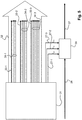
- both acoustic input signals 22 and 23 are applied via the transducer 12 underneath the sample 5.
- the both input signal parts 33 and 34 are provided to the transducer 12 as is schematically illustrated in figure 4 .
- the created indentations by the probe tip 9 at the surface of sample 5 may be picked up via the sensing system, providing an output signal 26 obtained via the optical detector 20.
- the embodiment of figure 4 has the further advantage of not requiring any further transducers other than the transducer 12 underneath the sample 5.
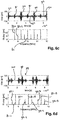
- the input signal consists of three groups of frequencies.
- a first group is formed by base signal component 81-1 at carrier frequency f c1 , and additional signal components 95-1 on either side thereof.
- a second group is formed by base signal component 81-2 at carrier frequency f c2 , and additional signal components 95-2 on either side thereof.
- a third group is formed by base signal component 81-3 at carrier frequency f c3 , and additional signal components 95-3 on either side thereof.
- the modulation frequency f m is 0.333 MHz for all groups.
- the time domain signal is identical to the situation in figure 6b , although the repetition frequency is different because the modulation frequency f m is 0.1 MHz - high power bursts 88 occur every 10 ⁇ s (microseconds), with seven small pulses 89 in between the high power bursts 88.
Landscapes
- Physics & Mathematics (AREA)
- General Health & Medical Sciences (AREA)
- Health & Medical Sciences (AREA)
- General Physics & Mathematics (AREA)
- Chemical & Material Sciences (AREA)
- Immunology (AREA)
- Biochemistry (AREA)
- Analytical Chemistry (AREA)
- Life Sciences & Earth Sciences (AREA)
- Pathology (AREA)
- Engineering & Computer Science (AREA)
- Nuclear Medicine, Radiotherapy & Molecular Imaging (AREA)
- Radiology & Medical Imaging (AREA)
- Acoustics & Sound (AREA)
- Power Engineering (AREA)
- Signal Processing (AREA)
- Nanotechnology (AREA)
- Investigating Or Analyzing Materials By The Use Of Ultrasonic Waves (AREA)
Priority Applications (5)
| Application Number | Priority Date | Filing Date | Title |
|---|---|---|---|
| EP19175565.1A EP3742178A1 (de) | 2019-05-21 | 2019-05-21 | Heterodynes rastersondenmikroskopieverfahren und rastersondenmikroskopiesystem |
| KR1020217040389A KR20220009406A (ko) | 2019-05-21 | 2020-05-22 | 헤테로다인 스캐닝 프로브 현미경 방법 및 스캐닝 프로브 현미경 시스템 |
| PCT/NL2020/050329 WO2020236002A1 (en) | 2019-05-21 | 2020-05-22 | Heterodyne scanning probe microscopy method and scanning probe microscopy system. |
| EP20730342.1A EP3973301B1 (de) | 2019-05-21 | 2020-05-22 | Heterodynes rastersondenmikroskopieverfahren und rastersondenmikroskopiesystem |
| US17/612,507 US11635448B2 (en) | 2019-05-21 | 2020-05-22 | Heterodyne scanning probe microscopy method and scanning probe microscopy system |
Applications Claiming Priority (1)
| Application Number | Priority Date | Filing Date | Title |
|---|---|---|---|
| EP19175565.1A EP3742178A1 (de) | 2019-05-21 | 2019-05-21 | Heterodynes rastersondenmikroskopieverfahren und rastersondenmikroskopiesystem |
Publications (2)
| Publication Number | Publication Date |
|---|---|
| EP3742178A1 true EP3742178A1 (de) | 2020-11-25 |
| EP3742178A8 EP3742178A8 (de) | 2021-02-24 |
Family
ID=66625825
Family Applications (2)
| Application Number | Title | Priority Date | Filing Date |
|---|---|---|---|
| EP19175565.1A Withdrawn EP3742178A1 (de) | 2019-05-21 | 2019-05-21 | Heterodynes rastersondenmikroskopieverfahren und rastersondenmikroskopiesystem |
| EP20730342.1A Active EP3973301B1 (de) | 2019-05-21 | 2020-05-22 | Heterodynes rastersondenmikroskopieverfahren und rastersondenmikroskopiesystem |
Family Applications After (1)
| Application Number | Title | Priority Date | Filing Date |
|---|---|---|---|
| EP20730342.1A Active EP3973301B1 (de) | 2019-05-21 | 2020-05-22 | Heterodynes rastersondenmikroskopieverfahren und rastersondenmikroskopiesystem |
Country Status (4)
| Country | Link |
|---|---|
| US (1) | US11635448B2 (de) |
| EP (2) | EP3742178A1 (de) |
| KR (1) | KR20220009406A (de) |
| WO (1) | WO2020236002A1 (de) |
Families Citing this family (1)
| Publication number | Priority date | Publication date | Assignee | Title |
|---|---|---|---|---|
| EP4375642A1 (de) | 2022-11-28 | 2024-05-29 | Nederlandse Organisatie voor toegepast-natuurwetenschappelijk Onderzoek TNO | Verfahren und system zur abbildung von untergrundeigenschaften in einem substrat |
Citations (3)
| Publication number | Priority date | Publication date | Assignee | Title |
|---|---|---|---|---|
| US20080276695A1 (en) * | 2007-05-10 | 2008-11-13 | Veeco Instruments Inc. | Non-destructive wafer-scale sub-surface ultrasonic microscopy employing near field afm detection |
| CN107219379A (zh) * | 2017-06-14 | 2017-09-29 | 广州市本原纳米仪器有限公司 | 一种多频扫描探针声学显微镜系统及其实现方法 |
| EP3349017A1 (de) * | 2017-01-13 | 2018-07-18 | Nederlandse Organisatie voor toegepast- natuurwetenschappelijk onderzoek TNO | Atomkraftmikroskopievorrichtung, -verfahren und lithographiesystem |
Family Cites Families (3)
| Publication number | Priority date | Publication date | Assignee | Title |
|---|---|---|---|---|
| US9417170B2 (en) * | 2011-07-15 | 2016-08-16 | Clarkson University | High resolution, high speed multi-frequency dynamic study of visco-elastic properites |
| EP3232192A1 (de) | 2016-04-14 | 2017-10-18 | Nederlandse Organisatie voor toegepast- natuurwetenschappelijk onderzoek TNO | Verfahren zur heterodynen rastersondenmikroskopie, rastersondenmikroskopiesystem und sonde dafür |
| EP3349020A1 (de) | 2017-01-13 | 2018-07-18 | Nederlandse Organisatie voor toegepast- natuurwetenschappelijk onderzoek TNO | Verfahren und system zur bildgebung von bereichen unterhalb der oberfläche mittels vibrationsmessungen |
-
2019
- 2019-05-21 EP EP19175565.1A patent/EP3742178A1/de not_active Withdrawn
-
2020
- 2020-05-22 WO PCT/NL2020/050329 patent/WO2020236002A1/en not_active Ceased
- 2020-05-22 US US17/612,507 patent/US11635448B2/en active Active
- 2020-05-22 EP EP20730342.1A patent/EP3973301B1/de active Active
- 2020-05-22 KR KR1020217040389A patent/KR20220009406A/ko active Pending
Patent Citations (3)
| Publication number | Priority date | Publication date | Assignee | Title |
|---|---|---|---|---|
| US20080276695A1 (en) * | 2007-05-10 | 2008-11-13 | Veeco Instruments Inc. | Non-destructive wafer-scale sub-surface ultrasonic microscopy employing near field afm detection |
| EP3349017A1 (de) * | 2017-01-13 | 2018-07-18 | Nederlandse Organisatie voor toegepast- natuurwetenschappelijk onderzoek TNO | Atomkraftmikroskopievorrichtung, -verfahren und lithographiesystem |
| CN107219379A (zh) * | 2017-06-14 | 2017-09-29 | 广州市本原纳米仪器有限公司 | 一种多频扫描探针声学显微镜系统及其实现方法 |
Also Published As
| Publication number | Publication date |
|---|---|
| US20220229088A1 (en) | 2022-07-21 |
| EP3973301A1 (de) | 2022-03-30 |
| EP3742178A8 (de) | 2021-02-24 |
| WO2020236002A1 (en) | 2020-11-26 |
| EP3973301B1 (de) | 2024-11-20 |
| US11635448B2 (en) | 2023-04-25 |
| KR20220009406A (ko) | 2022-01-24 |
Similar Documents
| Publication | Publication Date | Title |
|---|---|---|
| US11940416B2 (en) | Heterodyne scanning probe microscopy method and system | |
| TWI782972B (zh) | 用以執行次表面成像之方法及原子力顯微術系統 | |
| TWI766932B (zh) | 外差式原子力顯微術裝置、方法以及微影製程系統 | |
| KR102795394B1 (ko) | 진동 센싱을 이용하여 표면 하부 이미징을 수행하는 방법 및 시스템 | |
| US8869311B2 (en) | Displacement detection mechanism and scanning probe microscope using the same | |
| EP3973301B1 (de) | Heterodynes rastersondenmikroskopieverfahren und rastersondenmikroskopiesystem | |
| Almqvist et al. | Characterization of air-coupled ultrasound transducers in the frequency range 40 kHz–2 MHz using light diffraction tomography | |
| US20220205953A1 (en) | Method and system for imaging structures below the surface of a sample | |
| EP4143584B1 (de) | Verfahren, system und computerprogramm zur durchführung von akustischer rastersondenmikroskopie | |
| KR102581524B1 (ko) | 전자 빔에 의해 야기된 기판의 손상을 측정하는 방법 | |
| KR20210080509A (ko) | 표면 하부 원자힘 현미경을 위한 주파수 트래킹 | |
| JP3876316B2 (ja) | 表面波評価装置 | |
| WO2026018592A1 (ja) | 超音波検査装置及び超音波検査方法 | |
| Sathish et al. | Local phase measurements with focused acoustic transducer | |
| O’neill et al. | An array implementation of the resonance spectroscopy method for adhesive bonding imaging | |
| O'NEILL et al. | terization, Dept. of Physics, University of Windsor 401 Sunset Ave, N9B 3P4 |
Legal Events
| Date | Code | Title | Description |
|---|---|---|---|
| PUAI | Public reference made under article 153(3) epc to a published international application that has entered the european phase |
Free format text: ORIGINAL CODE: 0009012 |
|
| STAA | Information on the status of an ep patent application or granted ep patent |
Free format text: STATUS: THE APPLICATION HAS BEEN PUBLISHED |
|
| AK | Designated contracting states |
Kind code of ref document: A1 Designated state(s): AL AT BE BG CH CY CZ DE DK EE ES FI FR GB GR HR HU IE IS IT LI LT LU LV MC MK MT NL NO PL PT RO RS SE SI SK SM TR |
|
| AX | Request for extension of the european patent |
Extension state: BA ME |
|
| RIN1 | Information on inventor provided before grant (corrected) |
Inventor name: RAJADURAI, SRI RAM SHANKAR Inventor name: PIRAS, DANIELE Inventor name: SADEGHIAN MARNANI, HAMED Inventor name: VAN ES, MAARTEN HUBERTUS Inventor name: HATAKEYAMA, KODAI Inventor name: VAN NEER, PAUL LOUIS MARIA JOSEPH Inventor name: VAN DER LANS, MARCUS JOHANNES |
|
| STAA | Information on the status of an ep patent application or granted ep patent |
Free format text: STATUS: THE APPLICATION IS DEEMED TO BE WITHDRAWN |
|
| 18D | Application deemed to be withdrawn |
Effective date: 20210526 |